US7149155B2 - Channeled dielectric re-recordable data storage medium - Google Patents
Channeled dielectric re-recordable data storage medium Download PDFInfo
- Publication number
- US7149155B2 US7149155B2 US10/251,568 US25156802A US7149155B2 US 7149155 B2 US7149155 B2 US 7149155B2 US 25156802 A US25156802 A US 25156802A US 7149155 B2 US7149155 B2 US 7149155B2
- Authority
- US
- United States
- Prior art keywords
- medium
- dielectric material
- memory cell
- logical value
- phase
- Prior art date
- Legal status (The legal status is an assumption and is not a legal conclusion. Google has not performed a legal analysis and makes no representation as to the accuracy of the status listed.)
- Expired - Lifetime, expires
Links
- 238000013500 data storage Methods 0.000 title claims abstract description 35
- 239000000463 material Substances 0.000 claims abstract description 165
- 230000015654 memory Effects 0.000 claims abstract description 135
- 239000000945 filler Substances 0.000 claims abstract description 80
- 239000003989 dielectric material Substances 0.000 claims abstract description 60
- 210000004027 cell Anatomy 0.000 claims description 124
- 238000000034 method Methods 0.000 claims description 36
- 239000000758 substrate Substances 0.000 claims description 25
- 229910052751 metal Inorganic materials 0.000 claims description 16
- 239000004020 conductor Substances 0.000 claims description 15
- 239000002184 metal Substances 0.000 claims description 15
- 229910052782 aluminium Inorganic materials 0.000 claims description 14
- XAGFODPZIPBFFR-UHFFFAOYSA-N aluminium Chemical compound [Al] XAGFODPZIPBFFR-UHFFFAOYSA-N 0.000 claims description 14
- 238000000151 deposition Methods 0.000 claims description 13
- XUIMIQQOPSSXEZ-UHFFFAOYSA-N Silicon Chemical group [Si] XUIMIQQOPSSXEZ-UHFFFAOYSA-N 0.000 claims description 10
- 229910052710 silicon Inorganic materials 0.000 claims description 10
- 239000010703 silicon Substances 0.000 claims description 10
- 239000010405 anode material Substances 0.000 claims description 9
- 238000007254 oxidation reaction Methods 0.000 claims description 9
- 238000003860 storage Methods 0.000 claims description 8
- PNEYBMLMFCGWSK-UHFFFAOYSA-N aluminium oxide Inorganic materials [O-2].[O-2].[O-2].[Al+3].[Al+3] PNEYBMLMFCGWSK-UHFFFAOYSA-N 0.000 claims description 7
- 229910000838 Al alloy Inorganic materials 0.000 claims description 6
- ROFVEXUMMXZLPA-UHFFFAOYSA-N Bipyridyl Chemical compound N1=CC=CC=C1C1=CC=CC=N1 ROFVEXUMMXZLPA-UHFFFAOYSA-N 0.000 claims description 4
- 210000003850 cellular structure Anatomy 0.000 claims description 4
- 239000002105 nanoparticle Substances 0.000 claims description 4
- PCHJSUWPFVWCPO-UHFFFAOYSA-N gold Chemical compound [Au] PCHJSUWPFVWCPO-UHFFFAOYSA-N 0.000 claims description 3
- 229910052737 gold Inorganic materials 0.000 claims description 3
- 239000010931 gold Substances 0.000 claims description 3
- 239000001007 phthalocyanine dye Substances 0.000 claims description 2
- 239000011148 porous material Substances 0.000 claims description 2
- 229910052709 silver Inorganic materials 0.000 claims description 2
- 239000004332 silver Substances 0.000 claims description 2
- -1 silver halide Chemical class 0.000 claims description 2
- 238000007743 anodising Methods 0.000 claims 1
- RBTKNAXYKSUFRK-UHFFFAOYSA-N heliogen blue Chemical compound [Cu].[N-]1C2=C(C=CC=C3)C3=C1N=C([N-]1)C3=CC=CC=C3C1=NC([N-]1)=C(C=CC=C3)C3=C1N=C([N-]1)C3=CC=CC=C3C1=N2 RBTKNAXYKSUFRK-UHFFFAOYSA-N 0.000 claims 1
- 238000000059 patterning Methods 0.000 claims 1
- 238000010586 diagram Methods 0.000 description 6
- 238000010894 electron beam technology Methods 0.000 description 6
- 229910000618 GeSbTe Inorganic materials 0.000 description 5
- 150000001875 compounds Chemical class 0.000 description 3
- 230000003287 optical effect Effects 0.000 description 3
- 239000011149 active material Substances 0.000 description 2
- 238000002048 anodisation reaction Methods 0.000 description 2
- 230000000875 corresponding effect Effects 0.000 description 2
- AKUCEXGLFUSJCD-UHFFFAOYSA-N indium(3+);selenium(2-) Chemical compound [Se-2].[Se-2].[Se-2].[In+3].[In+3] AKUCEXGLFUSJCD-UHFFFAOYSA-N 0.000 description 2
- 239000003446 ligand Substances 0.000 description 2
- 238000004519 manufacturing process Methods 0.000 description 2
- KXJCPKFCPYCAHW-UHFFFAOYSA-N 3,4-bis(diphenylphosphanyl)furan-2,5-dione Chemical compound C=1C=CC=CC=1P(C=1C=CC=CC=1)C=1C(=O)OC(=O)C=1P(C=1C=CC=CC=1)C1=CC=CC=C1 KXJCPKFCPYCAHW-UHFFFAOYSA-N 0.000 description 1
- RYGMFSIKBFXOCR-UHFFFAOYSA-N Copper Chemical compound [Cu] RYGMFSIKBFXOCR-UHFFFAOYSA-N 0.000 description 1
- 229910005543 GaSe Inorganic materials 0.000 description 1
- GYHNNYVSQQEPJS-UHFFFAOYSA-N Gallium Chemical compound [Ga] GYHNNYVSQQEPJS-UHFFFAOYSA-N 0.000 description 1
- FYYHWMGAXLPEAU-UHFFFAOYSA-N Magnesium Chemical compound [Mg] FYYHWMGAXLPEAU-UHFFFAOYSA-N 0.000 description 1
- VYPSYNLAJGMNEJ-UHFFFAOYSA-N Silicium dioxide Chemical compound O=[Si]=O VYPSYNLAJGMNEJ-UHFFFAOYSA-N 0.000 description 1
- RTAQQCXQSZGOHL-UHFFFAOYSA-N Titanium Chemical compound [Ti] RTAQQCXQSZGOHL-UHFFFAOYSA-N 0.000 description 1
- SDGKDDBNEJYEAB-UHFFFAOYSA-N [Sb].[Ge].[Ag] Chemical compound [Sb].[Ge].[Ag] SDGKDDBNEJYEAB-UHFFFAOYSA-N 0.000 description 1
- 230000006978 adaptation Effects 0.000 description 1
- 229910045601 alloy Inorganic materials 0.000 description 1
- 239000000956 alloy Substances 0.000 description 1
- 238000001816 cooling Methods 0.000 description 1
- 229910052802 copper Inorganic materials 0.000 description 1
- 239000010949 copper Substances 0.000 description 1
- 230000002596 correlated effect Effects 0.000 description 1
- 230000008021 deposition Effects 0.000 description 1
- 229910052733 gallium Inorganic materials 0.000 description 1
- 229910052749 magnesium Inorganic materials 0.000 description 1
- 239000011777 magnesium Substances 0.000 description 1
- 239000007769 metal material Substances 0.000 description 1
- 150000002739 metals Chemical class 0.000 description 1
- 229910052758 niobium Inorganic materials 0.000 description 1
- 239000010955 niobium Substances 0.000 description 1
- GUCVJGMIXFAOAE-UHFFFAOYSA-N niobium atom Chemical compound [Nb] GUCVJGMIXFAOAE-UHFFFAOYSA-N 0.000 description 1
- TWNQGVIAIRXVLR-UHFFFAOYSA-N oxo(oxoalumanyloxy)alumane Chemical compound O=[Al]O[Al]=O TWNQGVIAIRXVLR-UHFFFAOYSA-N 0.000 description 1
- 238000009877 rendering Methods 0.000 description 1
- 229910052814 silicon oxide Inorganic materials 0.000 description 1
- 229910052715 tantalum Inorganic materials 0.000 description 1
- GUVRBAGPIYLISA-UHFFFAOYSA-N tantalum atom Chemical compound [Ta] GUVRBAGPIYLISA-UHFFFAOYSA-N 0.000 description 1
- XSOKHXFFCGXDJZ-UHFFFAOYSA-N telluride(2-) Chemical compound [Te-2] XSOKHXFFCGXDJZ-UHFFFAOYSA-N 0.000 description 1
- 229910052719 titanium Inorganic materials 0.000 description 1
- 239000010936 titanium Substances 0.000 description 1
Images


Classifications
-
- G—PHYSICS
- G11—INFORMATION STORAGE
- G11C—STATIC STORES
- G11C13/00—Digital stores characterised by the use of storage elements not covered by groups G11C11/00, G11C23/00, or G11C25/00
- G11C13/0002—Digital stores characterised by the use of storage elements not covered by groups G11C11/00, G11C23/00, or G11C25/00 using resistive RAM [RRAM] elements
- G11C13/0009—RRAM elements whose operation depends upon chemical change
-
- H—ELECTRICITY
- H10—SEMICONDUCTOR DEVICES; ELECTRIC SOLID-STATE DEVICES NOT OTHERWISE PROVIDED FOR
- H10B—ELECTRONIC MEMORY DEVICES
- H10B63/00—Resistance change memory devices, e.g. resistive RAM [ReRAM] devices
-
- G—PHYSICS
- G11—INFORMATION STORAGE
- G11C—STATIC STORES
- G11C13/00—Digital stores characterised by the use of storage elements not covered by groups G11C11/00, G11C23/00, or G11C25/00
- G11C13/0002—Digital stores characterised by the use of storage elements not covered by groups G11C11/00, G11C23/00, or G11C25/00 using resistive RAM [RRAM] elements
- G11C13/0004—Digital stores characterised by the use of storage elements not covered by groups G11C11/00, G11C23/00, or G11C25/00 using resistive RAM [RRAM] elements comprising amorphous/crystalline phase transition cells
Definitions
- Volatile memory loses its contents when power is no longer being supplied to the memory, whereas non-volatile memory maintains its contents even when power is not being supplied to the memory.
- RAM random-access memory
- IC integrated circuit
- data storage medium is used herein in a broad sense, and encompasses IC memory, as well as other types of data storage media.
- non-volatile memory has perhaps more commonly been available as and implemented as magnetic and optical media, including hard disk drives, floppy disks, compact disc read-only memories (CD-ROM's), CD re-writable (CD-RW) discs, and digital versatile discs (DVD's), among others.
- non-volatile memory implemented as an IC was primarily available as ROM that was not re-recordable, such as hard-wired ROM and programmable ROM (PROM). More recently, IC non-volatile memory has become available as various types of flash memory, which is more technically known as electrically erasable PROM (EEPROM).
- EEPROM electrically erasable PROM
- IC-based data storage media is typically read from and, where applicable, written to, using electric signals.
- magnetic and optical data storage media is typically read from, and where applicable, written to, using magnetic sensors and optical sensors, where the latter usually include some type of illuminating beam.
- a new type of data storage medium has been contemplated that can be implemented as an IC, but that is read from and written to using an illuminating beam.
- a phase-changeable layer is present that can be switched between two different phases by being subjected to the illuminating beam. The two phases correspond to different logical values, such as binary one and binary zero.
- the medium For reading the logical value stored in the phase-changeable layer, the medium is subjected to the illuminating beam at a low intensity. This induces current within the medium, which is then detected and correlated with the current phase of the re-recordable storage medium to determine the logical value stored in the medium.
- current may potentially leak from one memory cell of the medium to another, causing errors.
- the medium For writing a logical value to the phase-changeable layer, the medium is subjected to the illuminating beam at a high intensity. This causes the phase-changeable layer to switch from one phase to the other phase.
- the power needed to change the phase potentially may be relatively large, making the medium less desirable for environments in which power is a scarce resource.
- the invention relates to a re-recordable data storage medium.
- One embodiment of the medium includes dielectric material and filler material.
- the dielectric material is organized in columnar channels over which memory cells are logically distributed.
- the filler material is within the columnar channels to realize the memory cells.
- the filler material of each memory cell has at least a first configuration and a second configuration.
- the first configuration corresponds to a first storable logical value
- the second configuration corresponds to a second storable logical value.
- FIGS. 1A and 1B are diagrams showing a side view and a top view, respectively, of a re-recordable data storage medium, according to an embodiment of the invention.
- FIGS. 2A and 2B are diagrams showing different types of columnar channels of a re-recordable data storage medium, according to different embodiments of the invention.
- FIG. 3 is a diagram showing a re-recordable data storage medium in which a reduction-oxidation (redox) material is used to store different logical values, according to an embodiment of the invention, and that is consistent with the medium of FIGS. 1A and 1B .
- redox reduction-oxidation
- FIG. 4 is a diagram showing a re-recordable data storage medium in which a phase-changeable material is used to store different logical values, according to an embodiment of the invention, and that is consistent with the medium of FIGS. 1A and 1B .
- FIG. 5 is a flowchart showing a method for fabricating a re-recordable data storage medium, according to an embodiment of the invention.
- FIG. 6 is a flowchart showing a method for using a re-recordable data storage medium, according to an embodiment of the invention.
- FIG. 7 is a diagram of a mass storage device, according to an embodiment of the invention.
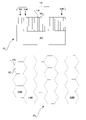
- FIGS. 1A and 1B show a side view and a top view, respectively, of a re-recordable data storage medium 100 , according to an embodiment of the invention.
- the medium 100 may be implemented as an integrated circuit (IC) and/or an electronic device, as well as other types of devices.
- the medium 100 in one embodiment has a substrate 102 that may be silicon or another material, and which can include the electronic and driving circuitry for the medium 100 .
- Filler material 106 within dielectric material 104 is positioned over the substrate 102 .
- the dielectric material 104 is organized into columnar channels 108 , including the channels 108 A, 108 B, . . . , 108 N.
- the dielectric material 104 is a dielectric at least in the sense that it separates the filler material 106 as filled in different of the columnar channels 108 .
- the filler material 106 is a filler at least in that it fills the columnar channels 108 into which the dielectric material 104 has been organized.
- the channels 108 thus are sidewalled by the dielectric material 104 , and are at least substantially filled with the filler material 106 .
- the dielectric material 104 may be a material that is anodized from its previous, non-anodized form, such that the resulting dielectric material 104 self-assembles into a cellular structure as the columnar channels 108 .
- One such anodic material is alumina, or aluminum oxide, which is anodized from aluminum, specifically from porous anodic aluminum.
- the dielectric material 104 is thus a porous material, such that it has the columnar channels 108 into which the filler material 106 can be deposited.
- the channels 108 are columnar in that they extend at least substantially vertically from bottom to top. Whereas the channels 108 are shown in FIG. 1B as uniformly hexagonal in shape, in other embodiments they may have other shapes, either uniform or non-uniform.
- the anodization process rendering the anodic material may result in at least two different types of the columnar channels 108 , according to varying embodiments of the invention. This is shown in FIGS. 2A and 2B .
- the columnar channel 108 A is shown in which the dielectric material 104 has been anodized such that the channel 108 A is at least substantially completely hollow. That is, the bottom 204 of the channel 108 A does not contain any of the dielectric material 104 .
- FIG. 2B the columnar channel 108 A is shown in which the dielectric material 104 has been anodized such that residual dielectric (anodic) material resides at the bottom 204 of the channel 108 A, as indicated by the reference number 206 .
- the filler material 106 is within the dielectric material 104 to realize memory cells of the medium 100 .
- the memory cells can have a one-to-one or a one-to-many correspondence with the columnar channels 108 . That is, in one embodiment, each of the channels 108 , as filled with the filler material 106 , corresponds to a memory cell, whereas in another embodiment, a given memory cell may encompass more than one of the channels 108 .
- the memory cells are thus distributed over the columnar channels 108 in a one-to-one or one-to-many fashion.
- the filler material 106 of each memory cell has at least two configurations corresponding to different storable logical values of the memory cell. For example, in a first configuration the filler material 106 may correspond to a logical value of zero, whereas in a second configuration the filler material 106 may correspond to a logical value of one.
- the dielectric material 104 separates the filler material 106 of different columnar channels 108 , and thus, in one embodiment, the filler material 106 of different memory cells. In other embodiments of the invention, there may be more than two configurations, such that more than two different logical values may be stored.
- the filler material 106 may in different embodiments be or include a phase-changeable material, a reduction-oxidation (redox) material, or another type of material.
- a phase-changeable material such material may be indium selenide, indium selenide telluride, or another phase-changeable material.
- phase-changeable materials include II-VI compounds, III-VI compounds, and ternary or quaternary compounds such as germanium antimony tellurium (GST) and silver germanium antimony tellurium.
- GST germanium antimony tellurium
- embodiments of the invention are not limited to this list of phase-changeable materials, and, as can be appreciated by those of ordinary skill within the art, this list is not exhaustive.
- Such a phase-changeable material has at least two phases, including, for instance, an at least substantially amorphous phase and an at least substantially crystalline phase. The different phases correspond to the different configurations of the filler material 106 .
- the redox material may be gold nanoparticles, silver halide nanoparticles, metal phthalocyanine dyes, Ru(bipy) 3 , Fe(CO) 3 L 2 , or another type of redox active material.
- the term “bipy” refers to 2,2′-bipyridyl ligand, whereas the term “L 2 ” refers to 2,3-bis(diphenylphosphino)maleic anhydride and similar bisphosphine bidentate ligands.
- Embodiments of the invention are not limited to this list of redox active materials, and, as can be appreciated by those of ordinary skill within the art, this list is not exhaustive.
- the redox material being reduced such that it can be said that the redox material is in a reduced state, corresponds to one of the configurations of the filler material 106 .
- the redox material being oxidized such that it can be said that the redox material is in an oxidized state, corresponds to another of the configurations of the filler material 106 .
- the redox material may be distributed throughout the filler material 106 , where the filler material 106 effectively acts as a carrier of the redox material.
- FIG. 3 shows the re-recordable data storage medium 100 , according to an embodiment in which a redox material is included within the filler material 106 .
- a redox material is included within the filler material 106 .
- an optional dielectric layer 302 and a conductive layer of blocks 304 such as metal, are present.
- the layer 302 may in one embodiment be patterned silicon oxide within the substrate 102 itself, where the dielectric layer 302 is not present, and where the substrate 102 is silicon.
- a conductive material 306 is deposited on the dielectric material 104 , but not on the filler material 106 , such as via a low-angle deposition approach.
- the material 306 thus includes the material 306 A, 306 B, 306 C, 306 D, . . . , 306 N.
- the material 306 may be aluminum, gold, or another type of metal or conductive material, and promotes reading of the memory cells.
- the conductive layer of blocks 304 is separably partitioned into conductive blocks, such as the blocks 304 A and 304 B, that assist erasure of the memory cells.
- Each of the conductive blocks encompasses a number of memory cells, such that the memory cells are organized into these blocks. For instance, where each of the columnar channels 108 corresponds to a separate memory cell, the block 304 A encompasses the memory cells of the channels 108 A, 108 B, and 108 C, and the block 304 B encompasses the memory cells of the channels 108 D, 108 E, and 108 N.
- the conductive layer of blocks 304 are thus also referred to as memory cell blocks.
- the dielectric layer 302 helps prevent shorting between the conductive layer of blocks 304 .
- FIG. 3 specifically shows the medium 100 where the dielectric material 104 is an anodic material, such as alumina.
- the material 104 ′ is aluminum, or partially anodized aluminum.
- a conductive material 306 ′ is deposited on the material 104 ′ when the conductive material 306 is deposited onto the dielectric material 104 .
- the presence of the material 104 ′ and the material 306 ′ do not affect the operation of the medium 100 , and are shown in FIG. 3 for illustrative completeness.
- the memory cell of the columnar channel 108 C is specifically shown in FIG. 3 as being written.
- the conductive material 306 and the conductive layer of blocks 304 are grounded.
- An illuminating beam 308 such as an electron beam, is applied to the filler material 106 of the columnar channel 108 C.
- the beam is at high energy, such as 50–2000 electron-volts (eV) in one embodiment of the invention, depending on the type of redox material used. This reduces the redox material, or component, within the filler material 106 , giving the filler material 106 a more negative charge, as indicated by the minus signs 312 .
- the cell can revert to the oxidized state, or erased, by a block-erasure process.
- the block-erasure process applied to the memory cell block 304 A erases the memory cells of the channels 108 A, 108 B, and 108 C
- the process applied to the block 304 B erases the cells of the channels 108 D, 108 E, and 108 N.
- the block-erasure process removes the negative charge stored in the filler material 106 of any of the memory cells, causing these memory cells to revert back to their oxidized states and store a different logical value than when they were in their reduced states.
- the conductive material 306 is grounded, and the memory cell block 304 A of the conductive layer of blocks 304 is biased at a high potential. This flushes the charge from the redox material within the filler material 106 within the channel 108 C in particular, without affecting the filler material 106 within the channels 108 A and 108 B, which have not been written.
- the redox material within the filler material 106 within the channel 108 C thus returns to the oxidized state. In this way, the memory cells of the columnar channels 108 can be block erased.
- the memory cells of the columnar channels 108 D and 108 E are specifically shown in FIG. 3 as being read.
- the conductive layer of blocks 304 is grounded, and the signal at the conductive material 306 is detected.
- the illuminating beams 310 A and 310 B such as electron beams, are applied to the filler material 106 of the columnar channels 108 D and 108 E.
- the beams 310 A and 310 B are at low energy, such as 20–2000 eV, in one embodiment of the invention, depending on the type of redox material being used.
- the memory cell of the channel 108 D is currently in a reduced state, and thus has a more negative charge, as indicated by the minus signs 314 .
- the memory cell of the channel 108 E conversely, is currently in an oxidized state, and thus has a less negative charge.
- the beam 310 A is deflected by the more negative charge of the filler material 106 within the channel 108 D to the conductive material 306 D.
- the beam 310 B is not deflected, since the filler material 106 within the channel 108 E is not as negatively charged. Therefore, when the memory cell of the channel 108 D is being read, a larger signal, or larger current, is present at the conductive material 306 than when the memory cell of the channel 108 E is being read. In this way, the two different logical values that can be stored in the memory cells of the columnar channels 108 can be distinguished from one another during reading.
- FIG. 4 shows the re-recordable data storage medium 100 , according to an embodiment of the invention in which the filler material 106 is a phase-changeable material.
- An optional conductive layer 402 such as metal, may be present on the dielectric material 104 and the filler material 106 , and when present can promote reading and writing to the memory cells.
- the embodiment of FIG. 4 specifically shows the medium 100 where the memory cells map to the columnar channels 108 , such as the channels 108 A, 108 B, . . . , 108 M, 108 N, on a one-to-one basis.
- the memory cells may also map to the channels 108 on a one-to-many basis, such that each cell encompasses more than one of the channels 108 .
- the memory cell of the columnar channel 108 B is specifically shown in FIG. 4 as being written.
- An illuminating beam 404 such as an electron beam, is applied to the filler material 106 of the columnar channel 108 B.
- the beam is at high power, using accelerating voltages such as 700–2000 eV, in one embodiment of the invention.
- the newly written (crystalline) phase of the filler material 106 is indicated in FIG. 4 by the shaded area 408 . In this way, two different logical values can be stored in the memory cells of the columnar channels 108 .
- the ending phase of the phase-changeable material depends on the rate at which the material is then cooled.
- the phase-changeable material is cooled relatively quickly, to avoid giving the material sufficient time to crystallize.
- the phase-changeable material is cooled relatively slowly, to give the material sufficient time to crystallize.
- the memory cells of the columnar channels 108 M and 108 N are specifically shown in FIG. 4 as being read.
- the illuminating beams 406 A and 406 B such as electron beams, are applied to the filler material 106 of the channels 108 M and 108 N.
- the beams 406 A and 406 B are at low power, using accelerating voltages such as 700–2000 eV, in one embodiment of the invention.
- the phase of the memory cell of the channel 108 M is currently crystalline, as indicated by the shaded area 410 , whereas the phase of the memory cell of the channel 108 N is currently amorphous.
- the signal, such as the current, at the medium 100 when reading the memory cell of the columnar channel 108 M is different than the signal at the medium 100 when reading the memory cell of the columnar channel 108 N. This is because the memory cells of the channels 108 M and 108 N are at different phases. In this way, the two different logical values that can be stored in the memory cells of the columnar channels 108 can be distinguished from one another during reading. Further, the dielectric material 104 separates the filler material 106 of the different channels 108 , substantially preventing shorting among adjacent memory cells during reading.
- FIG. 5 shows a method 500 for manufacturing a re-recordable data storage medium, according to an embodiment of the invention.
- the medium fabricated by performing the method 500 may be the medium 100 of one or more of the embodiments of FIGS. 1A–1B , 3 , and 4 .
- Some parts of the method 500 indicated as optional in FIG. 5 are particularly performed for fabricating the medium of the embodiment of FIG. 3 that utilizes a reduction-oxidation (redox) material within the filler material.
- Other parts of the method 500 indicated as optional in FIG. 5 are particularly performed for fabricating the medium of the embodiment of FIG. 4 that utilizes a phase-changeable material as the filler material.
- redox reduction-oxidation
- a dielectric layer is first optionally deposited or grown over a silicon substrate ( 502 ).
- a conductive metal layer is then deposited and patterned into memory cell blocks ( 504 ).
- the dielectric layer optionally deposited over the silicon substrate may be the dielectric layer 302 over the substrate 102 .
- the conductive metal layer deposited and patterned into memory cell blocks may be the conductive layer of blocks 304 patterned into blocks 304 A and 304 B.
- a metal is deposited ( 506 ), and anodized so that it self-assembles to form dielectric columnar channels ( 508 ).
- metals that can be so anodized include, but to which embodiments of the invention are not limited, aluminum, as well as alloys of aluminum, such as magnesium, tantalum, titanium, niobium, gallium, copper, and so on. Such aluminum and aluminum alloys can particularly be porous anodic aluminum and aluminum alloys, respectively.
- the metal is deposited and, once anodized, forms an oxide material. As such, the metal becomes the dielectric material 104 and forms the organized, columnar channels 108 .
- the dielectric material on the bottom of the columnar channels may optionally be etched ( 509 ).
- Filler material is then deposited within the channels to realize the memory cells ( 510 ).
- the filler material deposited within the channels to realize the memory cells may be the filler material 106 , when the method 500 is used to fabricate the medium 100 of FIGS. 1A–1B , 3 , and/or 4 .
- either a conductive material is low-angle deposited on the dielectric material, in the case where the medium being fabricated uses a redox material, or optionally a conductive layer is deposited over the dielectric material and the filler material, in the case where the medium being fabricated uses a phase-changeable material ( 512 ).
- the conductive material may be the conductive material 306 .
- the conductive layer may be the layer 402 .
- FIG. 6 shows a method 600 for using a re-recordable data storage medium 100 , according to an embodiment of the invention.
- the medium used by performing the method 600 may be the medium 100 of one or more of the embodiments of FIGS. 1A–1B , 3 , and 4 .
- redox reduction-oxidation
- an illuminating beam such as an electron beam
- a selected memory cell of the medium at low energy ( 608 ).
- a signal resulting from the beam illuminating on the medium is then detected ( 610 ).
- the signal is different depending on the configuration of the filler material of the selected memory cell. For instance, the signal may be substantially equal to a first, lower signal value with one configuration of the filler material, and substantially equal to a second, higher signal value with another configuration of the filler material.
- the signal is different depending on whether the redox material is in an oxidized or a reduced state.
- the signal is different depending on whether the phase-changeable material is in a crystalline or an amorphous phase.
- the different configurations of the filler material, such as the different states or phases of this material, correspond to different logical values being stored by the selected memory cell.
- the stored logical value in the selected memory cell is thus determined based on the signal that has been detected ( 612 ).
- the first, lower signal value may correspond to a logical value of zero being stored by the selected memory cell.
- the second lower, signal value would thus correspond to a logical value of one being stored by the selected memory cell.
- an illuminating beam such as an electron beam
- a selected memory cell of the medium is illuminated on a selected memory cell of the medium at high energy ( 614 ).
- the filler material includes a redox material
- its state can be changed from oxidized to reduced, although not vice-versa.
- the filler material is a phase-changeable material
- its phase may be changed from amorphous to crystalline, or vice-versa.
- This phase change is controlled by the rate at which the beam is turned off, and accordingly the rate of cooling of the selected memory cell depending on the value to be written thereto ( 617 ).
- the amorphous phase may correspond to one logical value
- the crystalline phase may correspond to another logical value.
- the material is cooled quickly, to not allow the material to have sufficient time to crystallize.
- the phase-changeable material result in the crystalline phase the material is cooled slowly, to allow the material to have sufficient time to crystallize.
- the block-erase action 606 is applicable where the filler material of the memory cells of the medium include a redox material.
- a high potential is applied to a selected memory cell block that includes a number of memory cells to be erased ( 616 ). Any of the memory cells within the block that were in the reduced state are erased back to the oxidized state. Memory cells within the block that were already in the oxidized state do not change.
- the block-erase action 606 is not applicable where the filler material of the memory cells of the medium are phase-changeable material, in which case the memory cells can be individually changed by re-writing them with the write action 604 .
- FIG. 7 shows a diagram of a rudimentary mass storage device 700 that can be used to read data from and write data to the re-recordable data storage medium 100 , according to an embodiment of the invention.
- the medium 100 may be the medium 100 of one or more of the embodiments of FIGS. 1A–1B , 3 , and 4 .
- the medium 100 is placed on a block 702 . More generally, the block 702 is an instance of a mechanism that is receptive to the storage medium 100 .
- An array of beam generators 704 corresponding to the memory cells of the medium 100 is positioned over the medium 100 , where preferably each beam generator corresponds to a cell of the medium 100 .
- the array of beam generators 704 may be a field array, or another type of array, of beam generators.
- a controller 708 is able to selectively turn on and off individual beams 706 of the array 704 , at varying desired intensities, for reading and writing logical values from and to memory cells of the medium 100 .
- the controller 708 is also able to detect the signal at the medium 100 , such as the current flowing through the storage medium 100 , for reading logical values stored in memory cells of the medium 100 , and able to bias different parts of the medium 100 as needed to read, write, or erase logical values of the memory cells of the medium 100 .
- the controller 708 more generally is an instance of a mechanism for performing this functionality. The reading, writing, and erasing performed by the controller 708 may be accomplished in accordance with the method 600 of FIG. 6 , as has been described.
Abstract
Description
Claims (40)
Priority Applications (4)
| Application Number | Priority Date | Filing Date | Title |
|---|---|---|---|
| US10/251,568 US7149155B2 (en) | 2002-09-20 | 2002-09-20 | Channeled dielectric re-recordable data storage medium |
| TW092120664A TW200405341A (en) | 2002-09-20 | 2003-07-29 | Channeled dielectric re-recordable data storage medium |
| JP2003297831A JP2004118997A (en) | 2002-09-20 | 2003-08-21 | Rewritable data storage medium, and method for constituting the same |
| EP03255492A EP1400979A3 (en) | 2002-09-20 | 2003-09-03 | Channeled dielectric re-recordable data storage medium |
Applications Claiming Priority (1)
| Application Number | Priority Date | Filing Date | Title |
|---|---|---|---|
| US10/251,568 US7149155B2 (en) | 2002-09-20 | 2002-09-20 | Channeled dielectric re-recordable data storage medium |
Publications (2)
| Publication Number | Publication Date |
|---|---|
| US20040057372A1 US20040057372A1 (en) | 2004-03-25 |
| US7149155B2 true US7149155B2 (en) | 2006-12-12 |
Family
ID=31946478
Family Applications (1)
| Application Number | Title | Priority Date | Filing Date |
|---|---|---|---|
| US10/251,568 Expired - Lifetime US7149155B2 (en) | 2002-09-20 | 2002-09-20 | Channeled dielectric re-recordable data storage medium |
Country Status (4)
| Country | Link |
|---|---|
| US (1) | US7149155B2 (en) |
| EP (1) | EP1400979A3 (en) |
| JP (1) | JP2004118997A (en) |
| TW (1) | TW200405341A (en) |
Cited By (4)
| Publication number | Priority date | Publication date | Assignee | Title |
|---|---|---|---|---|
| US20060046379A1 (en) * | 2004-08-30 | 2006-03-02 | Ralf Symanczyk | Fabricating memory components (PCRAMS) including memory cells based on a layer that changes phase state |
| US20070099309A1 (en) * | 2002-07-05 | 2007-05-03 | Samsung Electronics Co., Ltd. | High-density data storage medium, method of manufacturing the data storage medium, data storage apparatus, and methods of writing data on, and reading and erasing data from the data storage medium by using the data storage apparatus |
| US20090085023A1 (en) * | 2007-09-28 | 2009-04-02 | Ramachandran Muralidhar | Phase change memory structures |
| US20090085024A1 (en) * | 2007-09-28 | 2009-04-02 | Ramachandran Muralidhar | Phase change memory structures |
Families Citing this family (9)
| Publication number | Priority date | Publication date | Assignee | Title |
|---|---|---|---|---|
| US20060018240A1 (en) * | 2004-07-21 | 2006-01-26 | Charles Marshall | Digital media created using electron beam technology |
| US20060018238A1 (en) * | 2004-07-21 | 2006-01-26 | Trepl John A Ii | Fabrication of digital media using electron beam technology |
| US20060072428A1 (en) * | 2004-09-03 | 2006-04-06 | Charles Marshall | Fabrication of digital media using ion beam technology |
| US7701834B2 (en) * | 2005-01-18 | 2010-04-20 | Unity Semiconductor Corporation | Movable terminal in a two terminal memory array |
| FR2901909B1 (en) * | 2006-05-30 | 2008-10-24 | Commissariat Energie Atomique | INSCRIPTIBLE AND MICROPOINT-READABLE DATA MEMORY, BUILD-IN STRUCTURE, AND METHOD OF MANUFACTURE |
| JP4868518B2 (en) * | 2006-12-22 | 2012-02-01 | シャープ株式会社 | Resistance variable nonvolatile memory element, manufacturing method thereof, and nonvolatile semiconductor memory device |
| FR2915616B1 (en) * | 2007-04-27 | 2010-08-20 | Centre Nat Rech Scient | DEVICE AND METHOD FOR STORING INFORMATION MASS. |
| US7746680B2 (en) | 2007-12-27 | 2010-06-29 | Sandisk 3D, Llc | Three dimensional hexagonal matrix memory array |
| US7887999B2 (en) | 2007-12-27 | 2011-02-15 | Sandisk 3D Llc | Method of making a pillar pattern using triple or quadruple exposure |
Citations (14)
| Publication number | Priority date | Publication date | Assignee | Title |
|---|---|---|---|---|
| US4005452A (en) * | 1974-11-15 | 1977-01-25 | International Telephone And Telegraph Corporation | Method for providing electrical isolating material in selected regions of a semiconductive material and the product produced thereby |
| US4290843A (en) | 1980-02-19 | 1981-09-22 | Texas Instruments Incorporated | Epitaxial growth of magnetic memory film on implanted substrate |
| US5357399A (en) * | 1992-09-25 | 1994-10-18 | Avx Corporation | Mass production method for the manufacture of surface mount solid state capacitor and resulting capacitor |
| US5557596A (en) * | 1995-03-20 | 1996-09-17 | Gibson; Gary | Ultra-high density storage device |
| US5879955A (en) * | 1995-06-07 | 1999-03-09 | Micron Technology, Inc. | Method for fabricating an array of ultra-small pores for chalcogenide memory cells |
| US6045677A (en) | 1996-02-28 | 2000-04-04 | Nanosciences Corporation | Microporous microchannel plates and method of manufacturing same |
| US6243348B1 (en) * | 1998-06-05 | 2001-06-05 | Massachusetts Institute Of Technology | Very-high-density memory device utilizing a scintillating data-storage medium |
| US6258463B1 (en) * | 2000-03-02 | 2001-07-10 | Praxair S.T. Technology, Inc. | Anodized cryogenically treated aluminum |
| US6274463B1 (en) * | 2000-07-31 | 2001-08-14 | Hewlett-Packard Company | Fabrication of a photoconductive or a cathoconductive device using lateral solid overgrowth method |
| US6404647B1 (en) * | 2000-08-24 | 2002-06-11 | Hewlett-Packard Co. | Solid-state mass memory storage device |
| US6423621B2 (en) * | 1996-10-02 | 2002-07-23 | Micron Technology, Inc. | Controllable ovonic phase-change semiconductor memory device and methods of fabricating the same |
| US6607974B2 (en) * | 2000-07-14 | 2003-08-19 | Micron Technology, Inc. | Method of forming a contact structure in a semiconductor device |
| US6696355B2 (en) * | 2000-12-14 | 2004-02-24 | Ovonyx, Inc. | Method to selectively increase the top resistance of the lower programming electrode in a phase-change memory |
| US6700852B1 (en) * | 1999-06-04 | 2004-03-02 | Hitachi, Ltd. | Information recording medium with recording film with cobalt oxide crystalline particles, and information recording device including the same |
-
2002
- 2002-09-20 US US10/251,568 patent/US7149155B2/en not_active Expired - Lifetime
-
2003
- 2003-07-29 TW TW092120664A patent/TW200405341A/en unknown
- 2003-08-21 JP JP2003297831A patent/JP2004118997A/en not_active Withdrawn
- 2003-09-03 EP EP03255492A patent/EP1400979A3/en not_active Withdrawn
Patent Citations (14)
| Publication number | Priority date | Publication date | Assignee | Title |
|---|---|---|---|---|
| US4005452A (en) * | 1974-11-15 | 1977-01-25 | International Telephone And Telegraph Corporation | Method for providing electrical isolating material in selected regions of a semiconductive material and the product produced thereby |
| US4290843A (en) | 1980-02-19 | 1981-09-22 | Texas Instruments Incorporated | Epitaxial growth of magnetic memory film on implanted substrate |
| US5357399A (en) * | 1992-09-25 | 1994-10-18 | Avx Corporation | Mass production method for the manufacture of surface mount solid state capacitor and resulting capacitor |
| US5557596A (en) * | 1995-03-20 | 1996-09-17 | Gibson; Gary | Ultra-high density storage device |
| US5879955A (en) * | 1995-06-07 | 1999-03-09 | Micron Technology, Inc. | Method for fabricating an array of ultra-small pores for chalcogenide memory cells |
| US6045677A (en) | 1996-02-28 | 2000-04-04 | Nanosciences Corporation | Microporous microchannel plates and method of manufacturing same |
| US6423621B2 (en) * | 1996-10-02 | 2002-07-23 | Micron Technology, Inc. | Controllable ovonic phase-change semiconductor memory device and methods of fabricating the same |
| US6243348B1 (en) * | 1998-06-05 | 2001-06-05 | Massachusetts Institute Of Technology | Very-high-density memory device utilizing a scintillating data-storage medium |
| US6700852B1 (en) * | 1999-06-04 | 2004-03-02 | Hitachi, Ltd. | Information recording medium with recording film with cobalt oxide crystalline particles, and information recording device including the same |
| US6258463B1 (en) * | 2000-03-02 | 2001-07-10 | Praxair S.T. Technology, Inc. | Anodized cryogenically treated aluminum |
| US6607974B2 (en) * | 2000-07-14 | 2003-08-19 | Micron Technology, Inc. | Method of forming a contact structure in a semiconductor device |
| US6274463B1 (en) * | 2000-07-31 | 2001-08-14 | Hewlett-Packard Company | Fabrication of a photoconductive or a cathoconductive device using lateral solid overgrowth method |
| US6404647B1 (en) * | 2000-08-24 | 2002-06-11 | Hewlett-Packard Co. | Solid-state mass memory storage device |
| US6696355B2 (en) * | 2000-12-14 | 2004-02-24 | Ovonyx, Inc. | Method to selectively increase the top resistance of the lower programming electrode in a phase-change memory |
Cited By (12)
| Publication number | Priority date | Publication date | Assignee | Title |
|---|---|---|---|---|
| US20070099309A1 (en) * | 2002-07-05 | 2007-05-03 | Samsung Electronics Co., Ltd. | High-density data storage medium, method of manufacturing the data storage medium, data storage apparatus, and methods of writing data on, and reading and erasing data from the data storage medium by using the data storage apparatus |
| US7479212B2 (en) * | 2002-07-05 | 2009-01-20 | Samsung Electronics Co., Ltd. | Method of manufacturing high-density data storage medium |
| US20060046379A1 (en) * | 2004-08-30 | 2006-03-02 | Ralf Symanczyk | Fabricating memory components (PCRAMS) including memory cells based on a layer that changes phase state |
| US7329561B2 (en) * | 2004-08-30 | 2008-02-12 | Infineon Technologies, Ag | Fabricating memory components (PCRAMS) including memory cells based on a layer that changes phase state |
| US20090085023A1 (en) * | 2007-09-28 | 2009-04-02 | Ramachandran Muralidhar | Phase change memory structures |
| US20090085024A1 (en) * | 2007-09-28 | 2009-04-02 | Ramachandran Muralidhar | Phase change memory structures |
| WO2009045635A2 (en) * | 2007-09-28 | 2009-04-09 | Freescale Semiconductor Inc. | Phase change memory structures |
| WO2009045635A3 (en) * | 2007-09-28 | 2009-05-22 | Freescale Semiconductor Inc | Phase change memory structures |
| US7719039B2 (en) | 2007-09-28 | 2010-05-18 | Freescale Semiconductor, Inc. | Phase change memory structures including pillars |
| US7811851B2 (en) | 2007-09-28 | 2010-10-12 | Freescale Semiconductor, Inc. | Phase change memory structures |
| US20110001113A1 (en) * | 2007-09-28 | 2011-01-06 | Freescale Semiconductor, Inc. | Phase change memory structures |
| US8097873B2 (en) | 2007-09-28 | 2012-01-17 | Freescale Semiconductor, Inc. | Phase change memory structures |
Also Published As
| Publication number | Publication date |
|---|---|
| JP2004118997A (en) | 2004-04-15 |
| EP1400979A3 (en) | 2007-06-27 |
| EP1400979A2 (en) | 2004-03-24 |
| TW200405341A (en) | 2004-04-01 |
| US20040057372A1 (en) | 2004-03-25 |
Similar Documents
| Publication | Publication Date | Title |
|---|---|---|
| US7149155B2 (en) | Channeled dielectric re-recordable data storage medium | |
| KR100397929B1 (en) | Multi-bit single cell memory with tapered contacts | |
| US7227221B2 (en) | Multiple bit chalcogenide storage device | |
| US6908808B2 (en) | Method of forming and storing data in a multiple state memory cell | |
| US5536947A (en) | Electrically erasable, directly overwritable, multibit single cell memory element and arrays fabricated therefrom | |
| JP4933687B2 (en) | Composite memory material comprising a mixture of phase change memory material and dielectric material | |
| KR100371102B1 (en) | Programmable sub-surface aggregating metallization structure and method of making the same | |
| US5341328A (en) | Electrically erasable memory elements having reduced switching current requirements and increased write/erase cycle life | |
| US20100195371A1 (en) | Memory element and memory device | |
| KR20080005443A (en) | Non volatile memory cell and semiconductor memory device | |
| JP2003100085A (en) | Phase change type nonvolatile memory and its drive circuit | |
| Pandian et al. | Nanoscale Electrolytic Switching in Phase‐Change Chalcogenide Films | |
| US7061005B2 (en) | Phase-change random access memory device and method for manufacturing the same | |
| US7106622B2 (en) | Phase-change memory device capable of preprogramming memory cells optically and reading/writing memory cells electrically | |
| US20050259498A1 (en) | Asymmetrical programming mechanism for non-volatile memory | |
| JPWO2005031752A1 (en) | Multilevel memory and recording method for phase change recording medium therefor | |
| CN100382330C (en) | Unit structure for realizing multi-bit memory | |
| US20070008863A1 (en) | Memory comprising a memory device and a write unit configured as a probe | |
| US6937502B2 (en) | Re-recordable data storage medium utilizing conduction barrier | |
| CN114830238A (en) | Selective non-volatile memory device and associated read method | |
| KR20080061014A (en) | Programming of method phase change ram device |
Legal Events
| Date | Code | Title | Description |
|---|---|---|---|
| AS | Assignment |
Owner name: HEWLETT-PACKARD COMPANY, COLORADO Free format text: ASSIGNMENT OF ASSIGNORS INTEREST;ASSIGNORS:SCHUT, DAVID M.;GOVYADINOV, ALEXANDER;NOVET, THOMAS;AND OTHERS;REEL/FRAME:013761/0304;SIGNING DATES FROM 20020916 TO 20020920 |
|
| AS | Assignment |
Owner name: HEWLETT-PACKARD DEVELOPMENT COMPANY, L.P., COLORAD Free format text: ASSIGNMENT OF ASSIGNORS INTEREST;ASSIGNOR:HEWLETT-PACKARD COMPANY;REEL/FRAME:013776/0928 Effective date: 20030131 Owner name: HEWLETT-PACKARD DEVELOPMENT COMPANY, L.P.,COLORADO Free format text: ASSIGNMENT OF ASSIGNORS INTEREST;ASSIGNOR:HEWLETT-PACKARD COMPANY;REEL/FRAME:013776/0928 Effective date: 20030131 |
|
| STCF | Information on status: patent grant |
Free format text: PATENTED CASE |
|
| FPAY | Fee payment |
Year of fee payment: 4 |
|
| AS | Assignment |
Owner name: SAMSUNG ELECTRONICS CO., LTD., KOREA, REPUBLIC OF Free format text: ASSIGNMENT OF ASSIGNORS INTEREST;ASSIGNORS:HEWLETT-PACKARD DEVELOPMENT COMPANY, L.P.;HEWLETT-PACKARD COMPANY;REEL/FRAME:026008/0690 Effective date: 20100625 |
|
| FPAY | Fee payment |
Year of fee payment: 8 |
|
| MAFP | Maintenance fee payment |
Free format text: PAYMENT OF MAINTENANCE FEE, 12TH YEAR, LARGE ENTITY (ORIGINAL EVENT CODE: M1553) Year of fee payment: 12 |