US7159597B2 - Multistep remote plasma clean process - Google Patents
Multistep remote plasma clean process Download PDFInfo
- Publication number
- US7159597B2 US7159597B2 US10/153,315 US15331502A US7159597B2 US 7159597 B2 US7159597 B2 US 7159597B2 US 15331502 A US15331502 A US 15331502A US 7159597 B2 US7159597 B2 US 7159597B2
- Authority
- US
- United States
- Prior art keywords
- chamber
- gas
- substrate processing
- processing chamber
- plasma
- Prior art date
- Legal status (The legal status is an assumption and is not a legal conclusion. Google has not performed a legal analysis and makes no representation as to the accuracy of the status listed.)
- Expired - Fee Related, expires
Links
Images


Classifications
-
- B—PERFORMING OPERATIONS; TRANSPORTING
- B08—CLEANING
- B08B—CLEANING IN GENERAL; PREVENTION OF FOULING IN GENERAL
- B08B7/00—Cleaning by methods not provided for in a single other subclass or a single group in this subclass
- B08B7/0035—Cleaning by methods not provided for in a single other subclass or a single group in this subclass by radiant energy, e.g. UV, laser, light beam or the like
-
- C—CHEMISTRY; METALLURGY
- C23—COATING METALLIC MATERIAL; COATING MATERIAL WITH METALLIC MATERIAL; CHEMICAL SURFACE TREATMENT; DIFFUSION TREATMENT OF METALLIC MATERIAL; COATING BY VACUUM EVAPORATION, BY SPUTTERING, BY ION IMPLANTATION OR BY CHEMICAL VAPOUR DEPOSITION, IN GENERAL; INHIBITING CORROSION OF METALLIC MATERIAL OR INCRUSTATION IN GENERAL
- C23C—COATING METALLIC MATERIAL; COATING MATERIAL WITH METALLIC MATERIAL; SURFACE TREATMENT OF METALLIC MATERIAL BY DIFFUSION INTO THE SURFACE, BY CHEMICAL CONVERSION OR SUBSTITUTION; COATING BY VACUUM EVAPORATION, BY SPUTTERING, BY ION IMPLANTATION OR BY CHEMICAL VAPOUR DEPOSITION, IN GENERAL
- C23C16/00—Chemical coating by decomposition of gaseous compounds, without leaving reaction products of surface material in the coating, i.e. chemical vapour deposition [CVD] processes
- C23C16/44—Chemical coating by decomposition of gaseous compounds, without leaving reaction products of surface material in the coating, i.e. chemical vapour deposition [CVD] processes characterised by the method of coating
- C23C16/4401—Means for minimising impurities, e.g. dust, moisture or residual gas, in the reaction chamber
- C23C16/4405—Cleaning of reactor or parts inside the reactor by using reactive gases
-
- Y—GENERAL TAGGING OF NEW TECHNOLOGICAL DEVELOPMENTS; GENERAL TAGGING OF CROSS-SECTIONAL TECHNOLOGIES SPANNING OVER SEVERAL SECTIONS OF THE IPC; TECHNICAL SUBJECTS COVERED BY FORMER USPC CROSS-REFERENCE ART COLLECTIONS [XRACs] AND DIGESTS
- Y10—TECHNICAL SUBJECTS COVERED BY FORMER USPC
- Y10S—TECHNICAL SUBJECTS COVERED BY FORMER USPC CROSS-REFERENCE ART COLLECTIONS [XRACs] AND DIGESTS
- Y10S438/00—Semiconductor device manufacturing: process
- Y10S438/905—Cleaning of reaction chamber
Definitions
- a layer such as a silicon oxide layer
- a layer can be deposited by chemical vapor deposition (CVD).
- CVD chemical vapor deposition
- reactive gases are supplied to the substrate surface where heat-induced chemical reactions take place to form the desired film.
- a controlled plasma is formed using, for example, radio frequency (RF) energy or microwave energy to decompose and/or energize reactive species in reactant gases to produce the desired film.
- RF radio frequency
- Unwanted deposition on areas such as the walls of the processing chamber also occurs during such CVD processes.
- it is common to remove the unwanted deposition material that builds up on the interior of chamber walls with an in situ chamber clean operation.
- Common chamber cleaning techniques include the use of an etchant gas, such as fluorine, to remove the deposited material from the chamber walls and other areas.
- the etchant gas is introduced into the chamber and a plasma is formed so that the etchant gas reacts with and removes the deposited material from the chamber walls.
- Such cleaning procedures are commonly performed between deposition steps for every wafer or every n wafers.
- a remote plasma cleaning procedure may be employed in which an etchant plasma is generated remote from the substrate processing chamber by a high density plasma source such as a microwave plasma system, toroidal plasma generator or similar device. Dissociated species from the etchant plasma are then transported to the substrate processing chamber where they can react with and etch away the undesired deposition build up.
- Remote plasma cleaning procedures are sometimes used by manufacturers because they provide a “softer” etch than in situ plasma cleans, i.e., there is less ion bombardment and/or physical damage to chamber components because the plasma is not in contact with chamber components.
- remote plasma cleaning processes require a higher volume of etchant gas than is required by some in situ cleaning processes. Accordingly, improvements to remote plasma cleaning processes are desirable.
- Embodiments of the invention pertain to techniques for removing unwanted deposition build-up from one or more interior surfaces of a substrate processing chamber after a substrate is processed in the chamber by, for example, depositing a layer of material over the substrate.
- Embodiments of the invention use a reduced amount of etchant gas as compared to some remote plasma cleaning processes.
- a process for removing unwanted deposition build-up from one or more interior surfaces of a substrate processing chamber is provided.
- a substrate processed within the chamber is transferred out of the chamber:
- a first gas is introduced into the substrate processing chamber and an in situ plasma is formed within the chamber from the first gas in order to heat the chamber.
- the plasma is extinguished and an etchant gas is introduced into a remote plasma source fluidly coupled to the chamber. Reactive species are formed within the remote plasma source from the etchant gas and transported into the substrate processing chamber to etch the unwanted deposition build-up.
- a process for removing unwanted deposition build-up from one or more interior surfaces of a substrate processing chamber after a layer of material is deposited over a substrate disposed in the substrate processing chamber includes transferring the substrate out of the chamber; flowing an inert gas into the substrate processing chamber; forming a plasma from the inert gas within the substrate processing chamber to heat the chamber; thereafter, extinguishing the plasma, flowing an etchant gas into a remote plasma source at a first flow rate, forming reactive species from the etchant gas and transporting the reactive species into the substrate processing chamber to etch a first portion of the unwanted deposition build-up; and thereafter, decreasing the flow rate of the etchant gas into the remote plasma source while continuing to transport reactive species formed from the etchant gas into the substrate processing chamber to etch a second portion of the unwanted deposition build-up.
- FIG. 1A is a flowchart depicting the steps associated with one embodiment of the present invention.
- FIG. 1B is a flowchart depicting the steps associated with another embodiment of the present invention.
- FIG. 2 is a graph illustrating the increase in chamber temperature associated with increases in the duration of step 6 shown in FIGS. 1A and 1B ;
- FIG. 3 is a graph illustrating the increase in the clean rate of a remote plasma clean process executed after increasingly long in situ plasma heat-up steps
- FIG. 4 is a graph depicting the decrease in chamber temperature during the course of a remote plasma chamber clean process
- FIG. 5 is a graph illustrating an exemplary decrease in the flow rate of the etchant gas between remote plasma clean steps 8 A and 8 B in accordance with one embodiment of the invention
- FIG. 6 is a graph comparing the temperature of the interior of a chamber cleaned according to a previously known remote plasma clean process with the temperature of the interior of the chamber cleaned in accordance with techniques of the present invention
- FIG. 7A is a simplified, cross-sectional view of an exemplary substrate processing system with which embodiments of the present invention may be used;
- FIG. 7B is a simplified cross-sectional view of a gas ring that may be used in conjunction with the exemplary CVD processing chamber of FIG. 7A ;
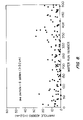
- FIG. 8 is a graph depicting test results in accordance with one embodiment of the present invention.
- FIGS. 9 and 10 are bar graphs comparing the length of time and total NF 3 usage, respectively, of a clean process in accordance with the present invention with a previously known remote plasma clean process.
- FIG. 1A is a flow chart depicting the steps according one embodiment of the present invention.
- a substrate deposition process or other type of substrate processing step step 2
- the substrate is transferred out of the chamber (step 4 ) and an in situ plasma is formed from a gas such as argon (step 6 ).
- the in situ plasma heats the substrate processing chamber (in some embodiments to a temperature above the deposition temperature used in the previous deposition step) prior to employing a remote plasma clean process.
- an appropriate temperature e.g., above 400° C.
- the in situ plasma is stopped and remotely dissociated species, such as fluorine-free radicals and other excited fluorine species, are transported into the chamber to etch the unwanted deposition build up from the chamber's interior (step 8 ).
- the plasma is stopped after a predetermined amount of time has elapsed.
- etchant gas usage e.g., NF 3
- NF 3 etchant gas usage
- in situ plasma preheating step 6 flows argon into the chamber at a flow rate of 40 sccm while the chamber is maintained at a pressure of about 5 mTorr.
- a plasma is formed from the argon by applying 3500 Watts of RF energy to the top coil and 4800 Watts of RF energy to the side coil. RF bias power is not employed and the plasma is maintained for 30 seconds to heat the chamber.
- argon flow rate of between 20–400 sccm
- chamber pressure between 2–10 mTorr
- top coil RF energy of between 1200–5000 Watts
- side coil RF energy of between 3500–5000 Watts and a length of between 20–60 seconds.
- inert gases other than argon can be used in other embodiments and in some other embodiments molecular oxygen or a similar oxygen source may be added to the argon or other inert gas flow or used in lieu of the inert gas.
- the in situ plasma heat-up step provides a highly effective heat source to increase the surface temperature on which the chemical reaction associated with the remote clean takes place.
- FIG. 2 shows the effect on chamber temperature as the heat up step proceeds.
- the temperature of a test silicon substrate (chucked to the pedestal and not cooled using a backside cooling technique) rises quickly during the first 60 seconds of the heat-up step until it reaches a near maximum value.
- the actual substrate temperature, as well as its rate of increase, will depend on the characteristics of the plasma, such as the amount of ion bombardment and the RF power levels employed, as a person of skill in the art will appreciate.
- FIG. 3 shows that as the chamber temperature increases due to longer in situ plasma heat-up steps, the clean rate of the subsequent remote plasma step also increases.
- An additional benefit achieved by the in situ plasma heat-up step is that sputtering generated from the argon onto oxide surfaces, such as unwanted silicon oxide deposition, may physically excite the uppermost layer of the oxide on both microscopic (i.e., surface roughness) and macroscopic (i.e., film stress and surface tension) levels, both of which promote the surface chemical reaction in large.
- FIG. 4 is a graph depicting the temperature of the chamber interior (measured at the pedestal) as a function of time during an exemplary remote plasma clean process.
- the temperature of the interior surfaces declines from an initial temperature of about 500° C. to a final temperature of about 100° C. during the course of the exemplary 10 minute remote plasma clean step.
- the chamber clean reaction is mass transport limited and thus higher clean gas flow rates generally result in faster clean times.
- the rate of the chamber clean step becomes surface reaction limited. Thus, higher clean gas rate flow rates do not correspond to higher clean rates.
- the dividing line between a mass transport limited reaction and a surface reaction limited reaction is approximated in FIG. 4 as time 20 . It is to be understood that the temperature and time values set forth in FIG. 4 , including dividing time 20 , are for exemplary purposes only. Actual temperatures, remote plasma clean times and dividing lines between the reaction mechanisms will differ depending on the application, the length of the in situ plasma clean step, the RF power levels employed, the gases employed and other factors as would be understood by a person of skill in the art.
- FIG. 1B The steps of another embodiment of the invention that uses the principle depicted in FIG. 4 to further reduce the amount of clean gas needed in order to adequately clean the chamber are shown in the flow chart of FIG. 1B .
- the embodiment of FIG. 1B is similar to that of FIG. 1A except that remote plasma clean step 8 is divided into two separate steps 8 A and 8 B.
- the first step of this two step process is a first remote plasma clean step in which the clean gas is flowed into the remote plasma generator at a first flow rate.
- the flow rate of the remote plasma clean gas e.g., a fluorine-containing etchant gas
- the initiation of remote plasma clean step 8 B corresponds generally to the diffusive dominating clean region (dividing time 20 in FIG. 4 ) so that the clean reaction rate can benefit from prolonged thermal effect of the plasm heat-up in combination with a chamber pressure effect.
- FIG. 5 shows one example of such a two-step remote plasma clean where the flow rate of NF 3 is reduced by 50% approximately halfway through the remote clean process (Point D).
- the reduction of the etchant gas may occur prior to or after the halfway mark of the reaction.
- the flow rate of the etchant gas may be stepped down from an initial high value to a final low value in multiple iterations. For example, in one embodiment, the flow rate may be successively reduced from 1000 sccm to 750 sccm to 500 sccm and then to 250 sccm before the clean process is completed.
- point B represents the start of remote plasma clean step 8 and point C represents the end of the remote plasma clean step.
- FIG. 6 shows one example of substrate processing chamber temperature as it varies over time from point A (the end of a deposition process), to point B (the end of the in situ plasma preheat step), to point C (the end of the remote clean process).
- line 30 represents a traditional remote plasma clean while line 32 represents a clean process according to one embodiment of the invention.
- the 20–60 additional seconds required by the preheat step is generally saved because of the higher clean rate by the remote plasma clean process, i.e., both processes have approximately the same overall duration.
- the time D at which the flow rate of the clean gas may be reduced in accordance with some embodiments of the invention as explained with respect to FIGS. 4 and 5 .
- Embodiments of the present invention can be implemented using a variety of substrate processing chambers providing the chambers have the capability creating reactive etch species within the chamber by forming an etchant plasma within the chamber (an in situ plasma) and by transporting remotely dissociated reactive species into the chamber from a remote plasma source in fluid communication with the chamber.
- An example of an inductively-coupled HDP-CVD chamber in which some embodiments of the method of the present invention can be practiced is set forth below. It is to be understood that the following chamber description is for exemplary purposes only as the techniques of the present invention can be used in a variety of other plasma chambers including PECVD chambers and ECR-HDP chambers among others.
- FIG. 7A illustrates one embodiment of a high density plasma chemical vapor deposition (HDP-CVD) system 110 in which the chamber cleaning techniques according to the present invention can be employed.
- System 110 includes a chamber 113 , a substrate support 118 , a gas delivery system 133 , a remote plasma cleaning system 150 , a vacuum system 170 , a source plasma system 180 A, a bias plasma system 180 B.
- HDP-CVD high density plasma chemical vapor deposition
- the upper portion of chamber 113 includes a dome 114 , which is made of a ceramic dielectric material, such as aluminum oxide or aluminum nitride. Dome 114 defines an upper boundary of a plasma processing region 116 .
- Plasma processing region 116 is bounded on the bottom by the upper surface of a substrate 117 and a substrate support 118 , which is also made from an aluminum oxide or aluminum ceramic material.
- a heater plate 123 and a cold plate 124 surmount, and are thermally coupled to, dome 114 .
- Heater plate 123 and cold plate 124 allow control of the dome temperature to within about ⁇ 10° C. over a range of about 100° C. to 200° C.
- exposure to the plasma heats a substrate positioned on substrate support 118 .
- Substrate support 118 includes inner and outer passages (not shown) that can deliver a heat transfer gas (sometimes referred to as a backside cooling gas) to the backside of the substrate.
- the lower portion of chamber 113 includes a body member 122 , which joins the chamber to the vacuum system.
- a base portion 121 of substrate support 118 is mounted on, and forms a continuous inner surface with, body member 122 .
- Substrates are transferred into and out of chamber 113 by a robot blade (not shown) through an insertion/removal opening (not shown) in the side of chamber 113 .
- Lift pins (not shown) are raised and then lowered under the control of a motor (also not shown) to move the substrate from the robot blade at an upper loading position 157 to a lower processing position 156 in which the substrate is placed on a substrate receiving portion 119 of substrate support 118 .
- Substrate receiving portion 119 includes an electrostatic chuck 120 that can be used to secure the substrate to substrate support 118 during substrate processing.
- Vacuum system 170 includes throttle body 125 , which houses twin-blade throttle valve 126 and is attached to gate valve 127 and turbo-molecular pump 128 .
- Gate valve 127 can isolate pump 128 from throttle body 125 , and can also control chamber pressure by restricting the exhaust flow capacity when throttle valve 126 is fully open.
- the arrangement of the throttle valve, gate valve, and turbo-molecular pump allow accurate and stable control of chamber pressures as low as about 1 mTorr.
- Source plasma system 180 A is coupled to a top coil 129 and side coil 130 , mounted on dome 114 .
- a symmetrical ground shield (not shown) reduces electrical coupling between the coils.
- Top coil 129 is powered by top source RF (SRF) generator 131 A
- side coil 130 is powered by side SRF generator 131 B, allowing independent power levels and frequencies of operation for each coil.
- the top source RF generator 131 A provides up to 2,500 watts of RF power at nominally 2 MHz and the side source RF generator 131 B provides up to 5,000 watts of RF power at nominally 2 MHz.
- the operating frequencies of the top and side RF generators may be offset from the nominal operating frequency (e.g. to 1.7–1.9 MHz and 1.9–2.1 MHz, respectively) to improve plasma-generation efficiency.
- a bias plasma system 180 B includes a bias RF (BRF) generator 131 C and a bias matching network 132 C.
- the bias plasma system 180 B capacitively couples substrate portion 117 to body member 122 , which act as complimentary electrodes.
- the bias plasma system 180 B serves to enhance the transport of plasma species (e.g., ions) created by the source plasma system 180 A to the surface of the substrate.
- bias RF generator provides up to 5,000 watts of RF power at 13.56 MHz.
- RF generators 131 A and 131 B include digitally controlled synthesizers and operate over a frequency range between about 1.8 to about 2.1 MHz. Each generator includes an RF control circuit (not shown) that measures reflected power from the chamber and coil back to the generator and adjusts the frequency of operation to obtain the lowest reflected power, as understood by a person of ordinary skill in the art.
- Matching networks 132 A and 132 B match the output impedance of generators 131 A and 131 B with their respective coils 129 and 130 .
- the RF control circuit may tune both matching networks by changing the value of capacitors within the matching networks to match the generator to the load as the load changes.
- the RF control circuit may tune a matching network when the power reflected from the load back to the generator exceeds a certain limit.
- One way to provide a constant match, and effectively disable the RF control circuit from tuning the matching network is to set the reflected power limit above any expected value of reflected power. This may help stabilize a plasma under some conditions by holding the matching network
- a gas delivery system 133 provides gases from several sources 134 ( a ) . . . 134 ( n ) via gas delivery lines 138 (only some of which are shown).
- gas sources 134 ( a ) . . . 134 ( n ) include separate sources for SiH 4 , O 2 , Ar and NF 3 as well as one or more sources for the extended cleaning process.
- the actual sources used for sources 134 ( a ) . . . 134 ( n ) and the actual connection of delivery lines 138 to chamber 113 varies depending on the deposition and cleaning processes executed within chamber 113 .
- Gas flow from each source 134 ( a ) . . . 134 ( n ) is controlled by one or more mass flow controllers (not shown) as is known to those of skill in the art.
- FIG. 7B is a simplified, partial cross-sectional view of chamber 113 showing additional details of gas ring 137 .
- one or more gas sources provide gas to ring plenum 136 in gas ring 137 via gas delivery lines 138 (only some of which are shown).
- Gas ring 137 has a plurality of gas nozzles 139 (only one of which is shown for purposes of illustration) that provides a uniform flow of gas over the substrate. Nozzle length and nozzle angle may be changed to allow tailoring of the uniformity profile and gas utilization efficiency for a particular process within an individual chamber.
- gas ring 137 has 24 (twenty-four) gas nozzles 139 made from an aluminum oxide ceramic.
- Gas ring 137 also has a plurality of gas nozzles 140 (only one of which is shown), which in a specific embodiment are co-planar with and shorter than source gas nozzles 139 , and in one embodiment receive gas from body plenum 141 .
- Gas nozzles 139 and 140 are not fluidly coupled in some embodiments where it is desirable to not mix gases (e.g., SiH 4 and O 2 ) introduced through gas ring 137 before injecting the gases into chamber 113 .
- gases may be mixed prior to injecting the gases into chamber 113 by providing apertures (not shown) between body plenum 141 and gas ring plenum 136 .
- Additional valves such as 143 B (other valves not shown), may shut off gas from the flow controllers to the chamber.
- valve 143 B to isolate chamber 113 from a delivery line 138 and to vent delivery line 138 to vacuum foreline 144 , for example.
- valve 143 A and 143 C may be incorporated on other gas delivery lines.
- Such 3-way valves may be placed as close to chamber 113 and remote plasma source 150 as practical, to minimize the volume of the unvented gas delivery line (between the 3-way valve and the chamber).
- two-way (on-off) valves may be placed between a mass flow controller (“MFC”) and the chamber or between a gas source and an MFC.
- MFC mass flow controller
- chamber 113 also has top nozzle 145 and top vent 146 .
- Top nozzle 145 and top vent 146 allow independent control of top and side flows of the gases, which improves film uniformity and allows fine adjustment of the film's deposition and doping parameters.
- Top vent 146 is an annular opening around top nozzle 145 .
- one source e.g., SiH 4
- separate MFCs may be used to control the flow of oxygen to both top vent 146 and gas nozzles 140 from a single source of oxygen.
- top nozzle 145 and top vent 146 may be kept separate prior to flowing the gases into chamber 113 , or the gases may be mixed in top plenum 148 before they flow into chamber 113 . In other embodiments, separate sources of the same gas may be used to supply various portions of the chamber.
- a remote plasma cleaning system such as a microwave plasma source 150 (or a torodial plasma source in other embodiments), is provided to periodically clean deposition residues from chamber components in a dry cleaning operation.
- the cleaning system includes a remote plasma generator 151 that creates a plasma from one or more cleaning gas source in sources 134 ( a ) . . . 134 ( n ) (e.g., molecular fluorine, nitrogen trifluoride, other fluorocarbons or equivalents alone or in combination with another gas such as Argon) in reactor cavity 153 .
- the reactive species resulting from this plasma are conveyed to chamber 113 through cleaning gas feed port 154 via applicator tube 155 .
- the materials used to contain the cleaning plasma must be resistant to attack by the plasma.
- the distance between reactor cavity 153 and feed port 154 should be kept as short as practical, since the concentration of desirable plasma species may decline with distance from reactor cavity 153 .
- Generating the cleaning plasma in a remote cavity does not subject chamber components to the temperature, radiation, or bombardment of the glow discharge that may be present in a plasma formed in situ. Consequently, relatively sensitive components, such as electrostatic chuck 120 , do not need to be covered with a dummy wafer or otherwise protected, as may be required with an in situ plasma cleaning process.
- System controller 160 controls the operation of system 110 .
- Controller 160 may include, for example, a memory 162 , such as a hard disk drive and/or a floppy disk drive and a card rack coupled to a processor 161 .
- the card rack may contain a single-board computer (SBC), analog and digital input/output boards, interface boards and stepper motor controller boards.
- SBC single-board computer
- System controller 160 operates under the control of a computer program stored on the hard disk drive or through other computer programs, such as programs stored on a removable disk.
- the computer program dictates, for example, the timing, mixture of gases, RF power levels and other parameters of a particular process.
- a 500-wafer marathon was run to check in-film particles, the direction indication of clean effectiveness, in an Ultima HDP-CVD chamber.
- the total clean time was 180 seconds including a 40 second in situ plasma heat-up step, a first 60 second remote plasma clean step and a second 80 second remote plasma clean step.
- Gas flow rates and other parameters used for the chamber clean portion of the 500 wafer marathon test are set forth below in Table 1.
- “TVO” means throttle valve fully open so that chamber pressure is controlled by the gas flow rate into the chamber.
- FIG. 8 shows that the average in-film particle adder is 6 for particle size greater than 0.2 microns. This particle performance is equivalent to that achieved by a previously used 180 second remote plasma chamber clean process that did not use the in situ plasma heat-up step according to the present invention.
- FIG. 9 is a bar graph that compares the timing of the various steps associated with the chamber cleaning process according to the present invention used in 500 wafer marathon test (process 40 ) with those associated with the previously used remote plasma chamber cleaning process (process 42 ). As is evident from FIG. 9 , even though process 40 includes an additional 40 second in situ plasma heat-up step, the total time required for each of processes 40 and 42 is equivalent.
- FIG. 10 is a graph comparing the total amount of NF 3 used in each of processes 40 and 42 in order to achieve substantially the same results.
- process 42 which does not use the techniques of the present invention, uses a total volume of 4500 standard cubic centimeters (scc) of NF 3 .
- Process 40 uses approximately 2200 scc of NF 3 —a 52% reduction as compared to the previously used process 42 .
Abstract
A process for removing unwanted deposition build-up from one or more interior surfaces of a substrate processing chamber after depositing a layer of material over a substrate disposed in the chamber. In one embodiment the process comprises transferring the substrate out of the chamber; flowing a first gas into the substrate processing chamber and forming a plasma within the chamber from the first gas in order to heat the chamber; and thereafter, extinguishing the plasma, flowing an etchant gas into a remote plasma source, forming reactive species from the etchant gas and transporting the reactive species into the substrate processing chamber to etch the unwanted deposition build-up.
Description
This application claims the benefit of U.S. Provisional Application No. 60/295,341, filed Jun. 1, 2001, which is incorporated herein by reference.
One of the primary steps in the fabrication of modern semiconductor devices is the formation of a layer, such as a silicon oxide layer, on a substrate or wafer. As is well known, such a layer can be deposited by chemical vapor deposition (CVD). In a conventional thermal CVD process, reactive gases are supplied to the substrate surface where heat-induced chemical reactions take place to form the desired film. In a conventional plasma CVD process, a controlled plasma is formed using, for example, radio frequency (RF) energy or microwave energy to decompose and/or energize reactive species in reactant gases to produce the desired film.
Unwanted deposition on areas such as the walls of the processing chamber also occurs during such CVD processes. As is known in the industry, it is common to remove the unwanted deposition material that builds up on the interior of chamber walls with an in situ chamber clean operation. Common chamber cleaning techniques include the use of an etchant gas, such as fluorine, to remove the deposited material from the chamber walls and other areas. In some processes, the etchant gas is introduced into the chamber and a plasma is formed so that the etchant gas reacts with and removes the deposited material from the chamber walls. Such cleaning procedures are commonly performed between deposition steps for every wafer or every n wafers.
Some semiconductor manufactures employ a remote plasma cleaning process as an alternative to an in situ plasma cleaning, a remote plasma cleaning procedure may be employed in which an etchant plasma is generated remote from the substrate processing chamber by a high density plasma source such as a microwave plasma system, toroidal plasma generator or similar device. Dissociated species from the etchant plasma are then transported to the substrate processing chamber where they can react with and etch away the undesired deposition build up. Remote plasma cleaning procedures are sometimes used by manufacturers because they provide a “softer” etch than in situ plasma cleans, i.e., there is less ion bombardment and/or physical damage to chamber components because the plasma is not in contact with chamber components.
One problem with some remote plasma cleaning processes, however, is that they require a higher volume of etchant gas than is required by some in situ cleaning processes. Accordingly, improvements to remote plasma cleaning processes are desirable.
Embodiments of the invention pertain to techniques for removing unwanted deposition build-up from one or more interior surfaces of a substrate processing chamber after a substrate is processed in the chamber by, for example, depositing a layer of material over the substrate. Embodiments of the invention use a reduced amount of etchant gas as compared to some remote plasma cleaning processes.
In accordance with one embodiment, a process for removing unwanted deposition build-up from one or more interior surfaces of a substrate processing chamber is provided. First, a substrate processed within the chamber is transferred out of the chamber: Next, a first gas is introduced into the substrate processing chamber and an in situ plasma is formed within the chamber from the first gas in order to heat the chamber. Once the chamber reaches a predetermined temperature or a predetermined period of time elapses, the plasma is extinguished and an etchant gas is introduced into a remote plasma source fluidly coupled to the chamber. Reactive species are formed within the remote plasma source from the etchant gas and transported into the substrate processing chamber to etch the unwanted deposition build-up.
In accordance with another embodiment, a process for removing unwanted deposition build-up from one or more interior surfaces of a substrate processing chamber after a layer of material is deposited over a substrate disposed in the substrate processing chamber is provided. The process includes transferring the substrate out of the chamber; flowing an inert gas into the substrate processing chamber; forming a plasma from the inert gas within the substrate processing chamber to heat the chamber; thereafter, extinguishing the plasma, flowing an etchant gas into a remote plasma source at a first flow rate, forming reactive species from the etchant gas and transporting the reactive species into the substrate processing chamber to etch a first portion of the unwanted deposition build-up; and thereafter, decreasing the flow rate of the etchant gas into the remote plasma source while continuing to transport reactive species formed from the etchant gas into the substrate processing chamber to etch a second portion of the unwanted deposition build-up.
These and other embodiments of the invention along with many of its advantages and features are described in more detail in conjunction with the text below and attached figures.
Embodiments of the present invention provide for an improved remote plasma cleaning process. FIG. 1A is a flow chart depicting the steps according one embodiment of the present invention. As shown in FIG. 1A , after a substrate deposition process or other type of substrate processing step (step 2) occurs in a substrate processing chamber, the substrate is transferred out of the chamber (step 4) and an in situ plasma is formed from a gas such as argon (step 6). The in situ plasma heats the substrate processing chamber (in some embodiments to a temperature above the deposition temperature used in the previous deposition step) prior to employing a remote plasma clean process. Once the chamber is heated to an appropriate temperature (e.g., above 400° C. in some embodiments), the in situ plasma is stopped and remotely dissociated species, such as fluorine-free radicals and other excited fluorine species, are transported into the chamber to etch the unwanted deposition build up from the chamber's interior (step 8). In other embodiments the plasma is stopped after a predetermined amount of time has elapsed.
The inventors have found that the addition of such an in situ plasma heat-up step prior to a remote plasma clean enhances the efficiency of the remote clean without sacrificing any of the desirable benefits achieved by such a “soft” clean. As a result, etchant gas usage (e.g., NF3) can be reduced significantly from the levels that may otherwise be required in a remote clean process to remove the same amount of deposition build-up.
In one embodiment implemented in an Ultima HDP-CVD chamber manufactured by Applied Materials and outfitted from 200 mm wafers, in situ plasma preheating step 6 flows argon into the chamber at a flow rate of 40 sccm while the chamber is maintained at a pressure of about 5 mTorr. A plasma is formed from the argon by applying 3500 Watts of RF energy to the top coil and 4800 Watts of RF energy to the side coil. RF bias power is not employed and the plasma is maintained for 30 seconds to heat the chamber. In some specific embodiments the following conditions are employed: an argon flow rate of between 20–400 sccm, a chamber pressure between 2–10 mTorr, top coil RF energy of between 1200–5000 Watts, side coil RF energy of between 3500–5000 Watts and a length of between 20–60 seconds. These ranges are for exemplary purposes only, however, and other embodiments may use values outside of these ranges or may use different parameters altogether. Also, inert gases other than argon can be used in other embodiments and in some other embodiments molecular oxygen or a similar oxygen source may be added to the argon or other inert gas flow or used in lieu of the inert gas.
As previously mentioned, the in situ plasma heat-up step provides a highly effective heat source to increase the surface temperature on which the chemical reaction associated with the remote clean takes place. FIG. 2 shows the effect on chamber temperature as the heat up step proceeds. As shown in FIG. 2 , the temperature of a test silicon substrate (chucked to the pedestal and not cooled using a backside cooling technique) rises quickly during the first 60 seconds of the heat-up step until it reaches a near maximum value. The actual substrate temperature, as well as its rate of increase, will depend on the characteristics of the plasma, such as the amount of ion bombardment and the RF power levels employed, as a person of skill in the art will appreciate.
During the remote clean reaction itself, the temperature of the chamber decreases from the temperature reached in the in situ plasma heat-up step to a lower temperature. This decrease in temperature effects the mechanisms that drives the clean reaction. This concept is illustrated in FIG. 4 , which is a graph depicting the temperature of the chamber interior (measured at the pedestal) as a function of time during an exemplary remote plasma clean process.
As shown in FIG. 4 , the temperature of the interior surfaces declines from an initial temperature of about 500° C. to a final temperature of about 100° C. during the course of the exemplary 10 minute remote plasma clean step. During the initial portion of the remote plasma clean process when the chamber is at relatively high temperature, the chamber clean reaction is mass transport limited and thus higher clean gas flow rates generally result in faster clean times. As the temperature of the chamber decreases, however, the rate of the chamber clean step becomes surface reaction limited. Thus, higher clean gas rate flow rates do not correspond to higher clean rates.
The dividing line between a mass transport limited reaction and a surface reaction limited reaction is approximated in FIG. 4 as time 20. It is to be understood that the temperature and time values set forth in FIG. 4 , including dividing time 20, are for exemplary purposes only. Actual temperatures, remote plasma clean times and dividing lines between the reaction mechanisms will differ depending on the application, the length of the in situ plasma clean step, the RF power levels employed, the gases employed and other factors as would be understood by a person of skill in the art.
The steps of another embodiment of the invention that uses the principle depicted in FIG. 4 to further reduce the amount of clean gas needed in order to adequately clean the chamber are shown in the flow chart of FIG. 1B . The embodiment of FIG. 1B is similar to that of FIG. 1A except that remote plasma clean step 8 is divided into two separate steps 8A and 8B. The first step of this two step process, is a first remote plasma clean step in which the clean gas is flowed into the remote plasma generator at a first flow rate. Then, in subsequent step 8B, the flow rate of the remote plasma clean gas (e.g., a fluorine-containing etchant gas) is reduced and/or the chamber pressure is lowered. In some embodiments, the initiation of remote plasma clean step 8B corresponds generally to the diffusive dominating clean region (dividing time 20 in FIG. 4 ) so that the clean reaction rate can benefit from prolonged thermal effect of the plasm heat-up in combination with a chamber pressure effect.
Embodiments of the present invention can be implemented using a variety of substrate processing chambers providing the chambers have the capability creating reactive etch species within the chamber by forming an etchant plasma within the chamber (an in situ plasma) and by transporting remotely dissociated reactive species into the chamber from a remote plasma source in fluid communication with the chamber. An example of an inductively-coupled HDP-CVD chamber in which some embodiments of the method of the present invention can be practiced is set forth below. It is to be understood that the following chamber description is for exemplary purposes only as the techniques of the present invention can be used in a variety of other plasma chambers including PECVD chambers and ECR-HDP chambers among others.
The upper portion of chamber 113 includes a dome 114, which is made of a ceramic dielectric material, such as aluminum oxide or aluminum nitride. Dome 114 defines an upper boundary of a plasma processing region 116. Plasma processing region 116 is bounded on the bottom by the upper surface of a substrate 117 and a substrate support 118, which is also made from an aluminum oxide or aluminum ceramic material.
A heater plate 123 and a cold plate 124 surmount, and are thermally coupled to, dome 114. Heater plate 123 and cold plate 124 allow control of the dome temperature to within about ±10° C. over a range of about 100° C. to 200° C. Generally, exposure to the plasma heats a substrate positioned on substrate support 118. Substrate support 118 includes inner and outer passages (not shown) that can deliver a heat transfer gas (sometimes referred to as a backside cooling gas) to the backside of the substrate.
The lower portion of chamber 113 includes a body member 122, which joins the chamber to the vacuum system. A base portion 121 of substrate support 118 is mounted on, and forms a continuous inner surface with, body member 122. Substrates are transferred into and out of chamber 113 by a robot blade (not shown) through an insertion/removal opening (not shown) in the side of chamber 113. Lift pins (not shown) are raised and then lowered under the control of a motor (also not shown) to move the substrate from the robot blade at an upper loading position 157 to a lower processing position 156 in which the substrate is placed on a substrate receiving portion 119 of substrate support 118. Substrate receiving portion 119 includes an electrostatic chuck 120 that can be used to secure the substrate to substrate support 118 during substrate processing.
A bias plasma system 180B includes a bias RF (BRF) generator 131C and a bias matching network 132C. The bias plasma system 180B capacitively couples substrate portion 117 to body member 122, which act as complimentary electrodes. The bias plasma system 180B serves to enhance the transport of plasma species (e.g., ions) created by the source plasma system 180A to the surface of the substrate. In a specific embodiment, bias RF generator provides up to 5,000 watts of RF power at 13.56 MHz.
A gas delivery system 133 provides gases from several sources 134(a) . . . 134(n) via gas delivery lines 138 (only some of which are shown). In the particular example illustrated below, gas sources 134(a) . . . 134(n) include separate sources for SiH4, O2, Ar and NF3 as well as one or more sources for the extended cleaning process. As would be understood by a person of skill in the art, the actual sources used for sources 134(a) . . . 134(n) and the actual connection of delivery lines 138 to chamber 113 varies depending on the deposition and cleaning processes executed within chamber 113. Gas flow from each source 134(a) . . . 134(n) is controlled by one or more mass flow controllers (not shown) as is known to those of skill in the art.
Gases are introduced into chamber 113 through a gas ring 137 and/or a top nozzle 145. FIG. 7B is a simplified, partial cross-sectional view of chamber 113 showing additional details of gas ring 137. In some embodiments, one or more gas sources provide gas to ring plenum 136 in gas ring 137 via gas delivery lines 138 (only some of which are shown). Gas ring 137 has a plurality of gas nozzles 139 (only one of which is shown for purposes of illustration) that provides a uniform flow of gas over the substrate. Nozzle length and nozzle angle may be changed to allow tailoring of the uniformity profile and gas utilization efficiency for a particular process within an individual chamber. In one specific embodiment, gas ring 137 has 24 (twenty-four) gas nozzles 139 made from an aluminum oxide ceramic.
In embodiments where flammable, toxic, or corrosive gases are used, it may be desirable to eliminate gas remaining in the gas delivery lines after a deposition or cleaning process. This may be accomplished using a 3-way valve, such as valve 143B, to isolate chamber 113 from a delivery line 138 and to vent delivery line 138 to vacuum foreline 144, for example. As shown in FIG. 7A , other similar valves, such as 143A and 143C, may be incorporated on other gas delivery lines. Such 3-way valves may be placed as close to chamber 113 and remote plasma source 150 as practical, to minimize the volume of the unvented gas delivery line (between the 3-way valve and the chamber). Additionally, two-way (on-off) valves (not shown) may be placed between a mass flow controller (“MFC”) and the chamber or between a gas source and an MFC.
Referring again to FIG. 7A , chamber 113 also has top nozzle 145 and top vent 146. Top nozzle 145 and top vent 146 allow independent control of top and side flows of the gases, which improves film uniformity and allows fine adjustment of the film's deposition and doping parameters. Top vent 146 is an annular opening around top nozzle 145. In one embodiment, one source, e.g., SiH4, supplies source gas nozzles 139 and top nozzle 145 through separate MFCs (not shown). Similarly, separate MFCs may be used to control the flow of oxygen to both top vent 146 and gas nozzles 140 from a single source of oxygen. The gases supplied to top nozzle 145 and top vent 146 may be kept separate prior to flowing the gases into chamber 113, or the gases may be mixed in top plenum 148 before they flow into chamber 113. In other embodiments, separate sources of the same gas may be used to supply various portions of the chamber.
A remote plasma cleaning system, such as a microwave plasma source 150 (or a torodial plasma source in other embodiments), is provided to periodically clean deposition residues from chamber components in a dry cleaning operation. The cleaning system includes a remote plasma generator 151 that creates a plasma from one or more cleaning gas source in sources 134(a) . . . 134(n) (e.g., molecular fluorine, nitrogen trifluoride, other fluorocarbons or equivalents alone or in combination with another gas such as Argon) in reactor cavity 153. The reactive species resulting from this plasma are conveyed to chamber 113 through cleaning gas feed port 154 via applicator tube 155. The materials used to contain the cleaning plasma (e.g., cavity 153 and applicator tube 155) must be resistant to attack by the plasma. The distance between reactor cavity 153 and feed port 154 should be kept as short as practical, since the concentration of desirable plasma species may decline with distance from reactor cavity 153. Generating the cleaning plasma in a remote cavity does not subject chamber components to the temperature, radiation, or bombardment of the glow discharge that may be present in a plasma formed in situ. Consequently, relatively sensitive components, such as electrostatic chuck 120, do not need to be covered with a dummy wafer or otherwise protected, as may be required with an in situ plasma cleaning process.
To validate the in situ plasma heat-up remote clean process just described, a 500-wafer marathon was run to check in-film particles, the direction indication of clean effectiveness, in an Ultima HDP-CVD chamber. The total clean time was 180 seconds including a 40 second in situ plasma heat-up step, a first 60 second remote plasma clean step and a second 80 second remote plasma clean step. Gas flow rates and other parameters used for the chamber clean portion of the 500 wafer marathon test are set forth below in Table 1. In Table 1, “TVO” means throttle valve fully open so that chamber pressure is controlled by the gas flow rate into the chamber.
| TABLE 1 |
| 500 WAFER MARATHON TEST |
| Param- | |||
| eter | Heat-up Step | |
|
| Gas | Ar (side) 300 sccm | NF3 | NF3 500 | sccm | |
| Ar (top) 30 |
1500 | sccm | |||
| Plasma | Top Coil 3000 W | 3200 | W (MW) | 2800 | W (MW) |
| Power | (RF) | ||||
| Side Coil 4000 W | |||||
| (RF) | |||||
| Pres- | 5 mTorr | 3.0 | Torr | TVO | |
| sure | 750 | | |||
| Time | |||||
| 40 |
60 | |
80 | sec | |
Having fully described several embodiments of the present invention, many other equivalents or alternative embodiments of the present invention will be apparent to those skilled in the art. For example, while the invention was described with respect to cleaning CVD chambers it may also be used to clean other types of chambers, including etch chambers, where appropriate. Also, why the examples set forth above all used NF3 as the etchant gases other etchant gases may be used in other embodiments. As such, the above description is illustrative and not restrictive. These equivalents and/or alternatives are intended to be included within the scope of the present invention.
Claims (23)
1. A process for removing unwanted deposition build-up from one or more interior surfaces of a substrate processing chamber after processing a substrate disposed in the substrate processing chamber, said process comprising:
transferring said substrate out of the chamber;
flowing a first gas into the substrate processing chamber and forming a plasma within the substrate processing chamber from the first gas to heat the chamber from a first temperature to a second, higher temperature;
thereafter, extinguishing the plasma, flowing an etchant gas into a remote plasma source, forming reactive species from the etchant gas and transporting the reactive species into the substrate processing chamber to etch the unwanted deposition build-up while allowing the chamber to drop to a temperature below the second temperature.
2. The process of claim 1 wherein the first gas consists of an inert gas.
3. The process of claim 1 wherein the first gas consists of an oxygen-containing source and/or an inert gas.
4. The process of claim 1 wherein the remote plasma source is a microwave plasma source.
5. The process of claim 1 wherein the remote plasma source is a toroidal plasma source.
6. The process of claim 1 wherein the step of forming the plasma within the chamber heats an interior surface of the chamber to a temperature of at least 400° C.
7. The process of claim 1 wherein the substrate processing chamber is a CVD chamber.
8. The process of claim 1 wherein the etchant gas comprises NF3.
9. A process for removing unwanted deposition build-up from one or more interior surfaces of a substrate processing chamber after depositing a layer of material over a substrate disposed in the substrate processing chamber, said process comprising:
transferring the substrate out of the chamber;
flowing an inert gas into the substrate processing chamber;
forming a plasma from the inert gas within the substrate processing chamber to heat the chamber;
thereafter, extinguishing the plasma, flowing an etchant gas into a remote plasma source at a first flow rate, forming reactive species from the etchant gas and transporting the reactive species into the substrate processing chamber to etch a first portion of the unwanted deposition build-up; and
thereafter, decreasing the flow rate of the etchant gas into the remote plasma source while continuing to transport reactive species formed from the etchant gas into the substrate processing chamber to etch a second portion of the unwanted deposition build-up.
10. The process of claim 9 wherein the inert gas is argon.
11. The process of claim 9 wherein the step of flowing an inert gas into the chamber further comprises flowing an oxygen-containing gas into the chamber.
12. The process of claim 9 wherein the remote plasma source is a microwave plasma source.
13. The process of claim 9 wherein the remote plasma source is a toroidal plasma source.
14. The process of claim 9 wherein the step of forming the plasma within the chamber heats an interior surface of the chamber to a temperature of at least 400C.
15. A process for removing unwanted deposition build-up from one or more interior surfaces of a substrate processing chamber after processing a substrate disposed in the substrate processing chamber, the process comprising:
transferring the substrate out of the chamber;
heating the substrate processing chamber by forming a plasma within the substrate processing chamber from a gas consisting essentially of inert gas constituents and/or and an oxygen-containing source to increase a surface temperature of the unwanted deposition build-up;
extinguishing the plasma within the chamber; and
removing the unwanted deposition build-up from one or more interior surfaces of a substrate processing chamber by flowing an etchant gas into a remote plasma source, forming reactive species from the etchant gas and transporting the reactive species into the substrate processing chamber.
16. The process of claim 15 wherein a temperature of the substrate processing chamber increases during the step of heating the chamber and decreases during the step of removing the unwanted deposition build-up.
17. The process of claim 16 further comprising, prior to transferring the substrate out of the chamber, depositing a layer of material over the substrate, wherein the step of heating the chamber increases the temperature of the chamber to a temperature beyond the temperature reached during the depositing step.
18. The process of claim 15 wherein the step of removing the unwanted deposition build-up comprises a phase in which a reaction between the reactive species and deposition build-up is mass transport limited followed by a phase in which a reaction between the reactive species and deposition build-up is surface reaction limited.
19. The process of claim 15 wherein the etchant gas comprises a fluorine source.
20. The process of claim 19 wherein the fluorine source comprises nitrogen trifluoride.
21. The process of claim 1 wherein the plasma formed from the first gas is formed by applying RF energy to a portion of the chamber.
22. The process of claim 1 wherein the first gas consists of an oxygen-containing source.
23. The process of claim 9 wherein a temperature of the substrate processing chamber increases during the step of forming a plasma within the substrate processing chamber and decreases while reactive species from the remote plasma source etch the first portion of the unwanted deposition build-up.
Priority Applications (1)
| Application Number | Priority Date | Filing Date | Title |
|---|---|---|---|
| US10/153,315 US7159597B2 (en) | 2001-06-01 | 2002-05-21 | Multistep remote plasma clean process |
Applications Claiming Priority (2)
| Application Number | Priority Date | Filing Date | Title |
|---|---|---|---|
| US29534101P | 2001-06-01 | 2001-06-01 | |
| US10/153,315 US7159597B2 (en) | 2001-06-01 | 2002-05-21 | Multistep remote plasma clean process |
Publications (2)
| Publication Number | Publication Date |
|---|---|
| US20030029475A1 US20030029475A1 (en) | 2003-02-13 |
| US7159597B2 true US7159597B2 (en) | 2007-01-09 |
Family
ID=26850416
Family Applications (1)
| Application Number | Title | Priority Date | Filing Date |
|---|---|---|---|
| US10/153,315 Expired - Fee Related US7159597B2 (en) | 2001-06-01 | 2002-05-21 | Multistep remote plasma clean process |
Country Status (1)
| Country | Link |
|---|---|
| US (1) | US7159597B2 (en) |
Cited By (11)
| Publication number | Priority date | Publication date | Assignee | Title |
|---|---|---|---|---|
| US20060005856A1 (en) * | 2004-06-29 | 2006-01-12 | Applied Materials, Inc. | Reduction of reactive gas attack on substrate heater |
| US20090071404A1 (en) * | 1997-12-24 | 2009-03-19 | Kunihiro Tada | Method of forming titanium film by CVD |
| US20100071719A1 (en) * | 2008-09-22 | 2010-03-25 | Taiwan Semiconductor Manufacturing Company, Ltd. | Method to pre-heat and stabilize etching chamber condition and improve mean time between cleaning |
| US20100087068A1 (en) * | 2008-10-07 | 2010-04-08 | Hitachi-Kokusai Electric Inc. | Method of manufacturing semiconductor device |
| US20100095979A1 (en) * | 2008-10-22 | 2010-04-22 | Applied Materials, Inc. | Remote plasma clean process with cycled high and low pressure clean steps |
| US20120171852A1 (en) * | 2009-09-04 | 2012-07-05 | Applied Materials, Inc | Remote hydrogen plasma source of silicon containing film deposition |
| US20140162338A1 (en) * | 2011-05-31 | 2014-06-12 | Leibniz-Institut Fuer Plasmaforschung Und Technologie E.V. | Device and method for producing a cold, homogeneous plasma under atmospheric pressure conditions |
| US20140326276A1 (en) * | 2013-05-01 | 2014-11-06 | Applied Materials, Inc. | Cobalt removal for chamber clean or pre-clean process |
| US8940099B2 (en) | 2012-04-02 | 2015-01-27 | Illinois Tool Works Inc. | Reflow oven and methods of treating surfaces of the reflow oven |
| US9170051B2 (en) | 2012-04-02 | 2015-10-27 | Illinois Tool Works Inc. | Reflow oven and methods of treating surfaces of the reflow oven |
| US11854773B2 (en) | 2020-03-31 | 2023-12-26 | Applied Materials, Inc. | Remote plasma cleaning of chambers for electronics manufacturing systems |
Families Citing this family (302)
| Publication number | Priority date | Publication date | Assignee | Title |
|---|---|---|---|---|
| US20040231695A1 (en) * | 2001-12-13 | 2004-11-25 | Hiromoto Ohno | Cleaning gas for semiconductor production equipment and cleaning method using the gas |
| US20080223409A1 (en) * | 2003-12-12 | 2008-09-18 | Horsky Thomas N | Method and apparatus for extending equipment uptime in ion implantation |
| KR100558550B1 (en) * | 2003-12-16 | 2006-03-10 | 삼성전자주식회사 | Method for cleaning phosphorus of plasma implant |
| US20050178333A1 (en) * | 2004-02-18 | 2005-08-18 | Asm Japan K.K. | System and method of CVD chamber cleaning |
| US20060021633A1 (en) * | 2004-07-27 | 2006-02-02 | Applied Materials, Inc. | Closed loop clean gas control |
| US7569111B2 (en) * | 2006-04-19 | 2009-08-04 | United Microelectronics Corp. | Method of cleaning deposition chamber |
| KR100819096B1 (en) * | 2006-11-21 | 2008-04-02 | 삼성전자주식회사 | Semiconductor manufacturing device for processing peox process and method for cleaning use remote plasma semiconductor manufacturing device |
| KR100886015B1 (en) * | 2007-05-15 | 2009-02-26 | 삼성전자주식회사 | Dry cleaning method of semiconductor production device having muti-lifter |
| US20090159104A1 (en) * | 2007-12-19 | 2009-06-25 | Judy Huang | Method and apparatus for chamber cleaning by in-situ plasma excitation |
| US10378106B2 (en) | 2008-11-14 | 2019-08-13 | Asm Ip Holding B.V. | Method of forming insulation film by modified PEALD |
| KR20100069392A (en) * | 2008-12-16 | 2010-06-24 | 삼성전자주식회사 | Manufacturing apparatus of semiconductor device detecting end point in deposition, etching or cleaning process by quartz crystal microbalance and manufacturing method using the same |
| US9394608B2 (en) | 2009-04-06 | 2016-07-19 | Asm America, Inc. | Semiconductor processing reactor and components thereof |
| US8802201B2 (en) | 2009-08-14 | 2014-08-12 | Asm America, Inc. | Systems and methods for thin-film deposition of metal oxides using excited nitrogen-oxygen species |
| JP5364514B2 (en) * | 2009-09-03 | 2013-12-11 | 東京エレクトロン株式会社 | Cleaning method in chamber |
| US10658161B2 (en) * | 2010-10-15 | 2020-05-19 | Applied Materials, Inc. | Method and apparatus for reducing particle defects in plasma etch chambers |
| US9312155B2 (en) | 2011-06-06 | 2016-04-12 | Asm Japan K.K. | High-throughput semiconductor-processing apparatus equipped with multiple dual-chamber modules |
| US10364496B2 (en) | 2011-06-27 | 2019-07-30 | Asm Ip Holding B.V. | Dual section module having shared and unshared mass flow controllers |
| US10854498B2 (en) | 2011-07-15 | 2020-12-01 | Asm Ip Holding B.V. | Wafer-supporting device and method for producing same |
| US20130023129A1 (en) | 2011-07-20 | 2013-01-24 | Asm America, Inc. | Pressure transmitter for a semiconductor processing environment |
| US9017481B1 (en) | 2011-10-28 | 2015-04-28 | Asm America, Inc. | Process feed management for semiconductor substrate processing |
| US9659799B2 (en) | 2012-08-28 | 2017-05-23 | Asm Ip Holding B.V. | Systems and methods for dynamic semiconductor process scheduling |
| US9021985B2 (en) | 2012-09-12 | 2015-05-05 | Asm Ip Holdings B.V. | Process gas management for an inductively-coupled plasma deposition reactor |
| US10714315B2 (en) | 2012-10-12 | 2020-07-14 | Asm Ip Holdings B.V. | Semiconductor reaction chamber showerhead |
| US9589770B2 (en) | 2013-03-08 | 2017-03-07 | Asm Ip Holding B.V. | Method and systems for in-situ formation of intermediate reactive species |
| US9484191B2 (en) | 2013-03-08 | 2016-11-01 | Asm Ip Holding B.V. | Pulsed remote plasma method and system |
| US9240412B2 (en) | 2013-09-27 | 2016-01-19 | Asm Ip Holding B.V. | Semiconductor structure and device and methods of forming same using selective epitaxial process |
| US10683571B2 (en) * | 2014-02-25 | 2020-06-16 | Asm Ip Holding B.V. | Gas supply manifold and method of supplying gases to chamber using same |
| US10167557B2 (en) | 2014-03-18 | 2019-01-01 | Asm Ip Holding B.V. | Gas distribution system, reactor including the system, and methods of using the same |
| US11015245B2 (en) | 2014-03-19 | 2021-05-25 | Asm Ip Holding B.V. | Gas-phase reactor and system having exhaust plenum and components thereof |
| US10858737B2 (en) | 2014-07-28 | 2020-12-08 | Asm Ip Holding B.V. | Showerhead assembly and components thereof |
| US9890456B2 (en) | 2014-08-21 | 2018-02-13 | Asm Ip Holding B.V. | Method and system for in situ formation of gas-phase compounds |
| US10941490B2 (en) | 2014-10-07 | 2021-03-09 | Asm Ip Holding B.V. | Multiple temperature range susceptor, assembly, reactor and system including the susceptor, and methods of using the same |
| US9657845B2 (en) | 2014-10-07 | 2017-05-23 | Asm Ip Holding B.V. | Variable conductance gas distribution apparatus and method |
| KR102263121B1 (en) | 2014-12-22 | 2021-06-09 | 에이에스엠 아이피 홀딩 비.브이. | Semiconductor device and manufacuring method thereof |
| TWI726863B (en) * | 2015-01-22 | 2021-05-11 | 家陞 陳 | Non-thermal soft plasma cleaning |
| US10529542B2 (en) | 2015-03-11 | 2020-01-07 | Asm Ip Holdings B.V. | Cross-flow reactor and method |
| US10276355B2 (en) | 2015-03-12 | 2019-04-30 | Asm Ip Holding B.V. | Multi-zone reactor, system including the reactor, and method of using the same |
| US10458018B2 (en) | 2015-06-26 | 2019-10-29 | Asm Ip Holding B.V. | Structures including metal carbide material, devices including the structures, and methods of forming same |
| US10600673B2 (en) | 2015-07-07 | 2020-03-24 | Asm Ip Holding B.V. | Magnetic susceptor to baseplate seal |
| US10083836B2 (en) | 2015-07-24 | 2018-09-25 | Asm Ip Holding B.V. | Formation of boron-doped titanium metal films with high work function |
| US9960072B2 (en) | 2015-09-29 | 2018-05-01 | Asm Ip Holding B.V. | Variable adjustment for precise matching of multiple chamber cavity housings |
| US10211308B2 (en) | 2015-10-21 | 2019-02-19 | Asm Ip Holding B.V. | NbMC layers |
| US10322384B2 (en) | 2015-11-09 | 2019-06-18 | Asm Ip Holding B.V. | Counter flow mixer for process chamber |
| US11139308B2 (en) | 2015-12-29 | 2021-10-05 | Asm Ip Holding B.V. | Atomic layer deposition of III-V compounds to form V-NAND devices |
| US10529554B2 (en) | 2016-02-19 | 2020-01-07 | Asm Ip Holding B.V. | Method for forming silicon nitride film selectively on sidewalls or flat surfaces of trenches |
| US10468251B2 (en) | 2016-02-19 | 2019-11-05 | Asm Ip Holding B.V. | Method for forming spacers using silicon nitride film for spacer-defined multiple patterning |
| US10501866B2 (en) | 2016-03-09 | 2019-12-10 | Asm Ip Holding B.V. | Gas distribution apparatus for improved film uniformity in an epitaxial system |
| US10343920B2 (en) | 2016-03-18 | 2019-07-09 | Asm Ip Holding B.V. | Aligned carbon nanotubes |
| US9892913B2 (en) | 2016-03-24 | 2018-02-13 | Asm Ip Holding B.V. | Radial and thickness control via biased multi-port injection settings |
| US10190213B2 (en) | 2016-04-21 | 2019-01-29 | Asm Ip Holding B.V. | Deposition of metal borides |
| US10865475B2 (en) | 2016-04-21 | 2020-12-15 | Asm Ip Holding B.V. | Deposition of metal borides and silicides |
| US10032628B2 (en) | 2016-05-02 | 2018-07-24 | Asm Ip Holding B.V. | Source/drain performance through conformal solid state doping |
| US10367080B2 (en) | 2016-05-02 | 2019-07-30 | Asm Ip Holding B.V. | Method of forming a germanium oxynitride film |
| KR102592471B1 (en) | 2016-05-17 | 2023-10-20 | 에이에스엠 아이피 홀딩 비.브이. | Method of forming metal interconnection and method of fabricating semiconductor device using the same |
| US11453943B2 (en) | 2016-05-25 | 2022-09-27 | Asm Ip Holding B.V. | Method for forming carbon-containing silicon/metal oxide or nitride film by ALD using silicon precursor and hydrocarbon precursor |
| US10388509B2 (en) | 2016-06-28 | 2019-08-20 | Asm Ip Holding B.V. | Formation of epitaxial layers via dislocation filtering |
| US10612137B2 (en) | 2016-07-08 | 2020-04-07 | Asm Ip Holdings B.V. | Organic reactants for atomic layer deposition |
| US9859151B1 (en) | 2016-07-08 | 2018-01-02 | Asm Ip Holding B.V. | Selective film deposition method to form air gaps |
| US10714385B2 (en) | 2016-07-19 | 2020-07-14 | Asm Ip Holding B.V. | Selective deposition of tungsten |
| US10381226B2 (en) | 2016-07-27 | 2019-08-13 | Asm Ip Holding B.V. | Method of processing substrate |
| KR102532607B1 (en) | 2016-07-28 | 2023-05-15 | 에이에스엠 아이피 홀딩 비.브이. | Substrate processing apparatus and method of operating the same |
| US9812320B1 (en) | 2016-07-28 | 2017-11-07 | Asm Ip Holding B.V. | Method and apparatus for filling a gap |
| US9887082B1 (en) | 2016-07-28 | 2018-02-06 | Asm Ip Holding B.V. | Method and apparatus for filling a gap |
| US10395919B2 (en) | 2016-07-28 | 2019-08-27 | Asm Ip Holding B.V. | Method and apparatus for filling a gap |
| US10858727B2 (en) | 2016-08-19 | 2020-12-08 | Applied Materials, Inc. | High density, low stress amorphous carbon film, and process and equipment for its deposition |
| US10410943B2 (en) | 2016-10-13 | 2019-09-10 | Asm Ip Holding B.V. | Method for passivating a surface of a semiconductor and related systems |
| US10643826B2 (en) | 2016-10-26 | 2020-05-05 | Asm Ip Holdings B.V. | Methods for thermally calibrating reaction chambers |
| US11532757B2 (en) | 2016-10-27 | 2022-12-20 | Asm Ip Holding B.V. | Deposition of charge trapping layers |
| US10229833B2 (en) | 2016-11-01 | 2019-03-12 | Asm Ip Holding B.V. | Methods for forming a transition metal nitride film on a substrate by atomic layer deposition and related semiconductor device structures |
| US10643904B2 (en) | 2016-11-01 | 2020-05-05 | Asm Ip Holdings B.V. | Methods for forming a semiconductor device and related semiconductor device structures |
| US10435790B2 (en) | 2016-11-01 | 2019-10-08 | Asm Ip Holding B.V. | Method of subatmospheric plasma-enhanced ALD using capacitively coupled electrodes with narrow gap |
| US10714350B2 (en) | 2016-11-01 | 2020-07-14 | ASM IP Holdings, B.V. | Methods for forming a transition metal niobium nitride film on a substrate by atomic layer deposition and related semiconductor device structures |
| US10134757B2 (en) | 2016-11-07 | 2018-11-20 | Asm Ip Holding B.V. | Method of processing a substrate and a device manufactured by using the method |
| KR102546317B1 (en) | 2016-11-15 | 2023-06-21 | 에이에스엠 아이피 홀딩 비.브이. | Gas supply unit and substrate processing apparatus including the same |
| US10340135B2 (en) | 2016-11-28 | 2019-07-02 | Asm Ip Holding B.V. | Method of topologically restricted plasma-enhanced cyclic deposition of silicon or metal nitride |
| KR20180068582A (en) | 2016-12-14 | 2018-06-22 | 에이에스엠 아이피 홀딩 비.브이. | Substrate processing apparatus |
| US11447861B2 (en) | 2016-12-15 | 2022-09-20 | Asm Ip Holding B.V. | Sequential infiltration synthesis apparatus and a method of forming a patterned structure |
| US11581186B2 (en) | 2016-12-15 | 2023-02-14 | Asm Ip Holding B.V. | Sequential infiltration synthesis apparatus |
| KR20180070971A (en) | 2016-12-19 | 2018-06-27 | 에이에스엠 아이피 홀딩 비.브이. | Substrate processing apparatus |
| US10269558B2 (en) | 2016-12-22 | 2019-04-23 | Asm Ip Holding B.V. | Method of forming a structure on a substrate |
| US10867788B2 (en) | 2016-12-28 | 2020-12-15 | Asm Ip Holding B.V. | Method of forming a structure on a substrate |
| US10655221B2 (en) | 2017-02-09 | 2020-05-19 | Asm Ip Holding B.V. | Method for depositing oxide film by thermal ALD and PEALD |
| US10468261B2 (en) | 2017-02-15 | 2019-11-05 | Asm Ip Holding B.V. | Methods for forming a metallic film on a substrate by cyclical deposition and related semiconductor device structures |
| US10283353B2 (en) | 2017-03-29 | 2019-05-07 | Asm Ip Holding B.V. | Method of reforming insulating film deposited on substrate with recess pattern |
| US10529563B2 (en) | 2017-03-29 | 2020-01-07 | Asm Ip Holdings B.V. | Method for forming doped metal oxide films on a substrate by cyclical deposition and related semiconductor device structures |
| KR102457289B1 (en) | 2017-04-25 | 2022-10-21 | 에이에스엠 아이피 홀딩 비.브이. | Method for depositing a thin film and manufacturing a semiconductor device |
| US10892156B2 (en) | 2017-05-08 | 2021-01-12 | Asm Ip Holding B.V. | Methods for forming a silicon nitride film on a substrate and related semiconductor device structures |
| US10770286B2 (en) | 2017-05-08 | 2020-09-08 | Asm Ip Holdings B.V. | Methods for selectively forming a silicon nitride film on a substrate and related semiconductor device structures |
| US10446393B2 (en) | 2017-05-08 | 2019-10-15 | Asm Ip Holding B.V. | Methods for forming silicon-containing epitaxial layers and related semiconductor device structures |
| US10504742B2 (en) | 2017-05-31 | 2019-12-10 | Asm Ip Holding B.V. | Method of atomic layer etching using hydrogen plasma |
| US10886123B2 (en) | 2017-06-02 | 2021-01-05 | Asm Ip Holding B.V. | Methods for forming low temperature semiconductor layers and related semiconductor device structures |
| US11306395B2 (en) | 2017-06-28 | 2022-04-19 | Asm Ip Holding B.V. | Methods for depositing a transition metal nitride film on a substrate by atomic layer deposition and related deposition apparatus |
| US10685834B2 (en) | 2017-07-05 | 2020-06-16 | Asm Ip Holdings B.V. | Methods for forming a silicon germanium tin layer and related semiconductor device structures |
| KR20190009245A (en) | 2017-07-18 | 2019-01-28 | 에이에스엠 아이피 홀딩 비.브이. | Methods for forming a semiconductor device structure and related semiconductor device structures |
| US11018002B2 (en) | 2017-07-19 | 2021-05-25 | Asm Ip Holding B.V. | Method for selectively depositing a Group IV semiconductor and related semiconductor device structures |
| US10541333B2 (en) | 2017-07-19 | 2020-01-21 | Asm Ip Holding B.V. | Method for depositing a group IV semiconductor and related semiconductor device structures |
| US11374112B2 (en) | 2017-07-19 | 2022-06-28 | Asm Ip Holding B.V. | Method for depositing a group IV semiconductor and related semiconductor device structures |
| US10605530B2 (en) | 2017-07-26 | 2020-03-31 | Asm Ip Holding B.V. | Assembly of a liner and a flange for a vertical furnace as well as the liner and the vertical furnace |
| US10312055B2 (en) | 2017-07-26 | 2019-06-04 | Asm Ip Holding B.V. | Method of depositing film by PEALD using negative bias |
| US10590535B2 (en) | 2017-07-26 | 2020-03-17 | Asm Ip Holdings B.V. | Chemical treatment, deposition and/or infiltration apparatus and method for using the same |
| US10692741B2 (en) | 2017-08-08 | 2020-06-23 | Asm Ip Holdings B.V. | Radiation shield |
| US10770336B2 (en) | 2017-08-08 | 2020-09-08 | Asm Ip Holding B.V. | Substrate lift mechanism and reactor including same |
| US11139191B2 (en) | 2017-08-09 | 2021-10-05 | Asm Ip Holding B.V. | Storage apparatus for storing cassettes for substrates and processing apparatus equipped therewith |
| US10249524B2 (en) | 2017-08-09 | 2019-04-02 | Asm Ip Holding B.V. | Cassette holder assembly for a substrate cassette and holding member for use in such assembly |
| US11769682B2 (en) | 2017-08-09 | 2023-09-26 | Asm Ip Holding B.V. | Storage apparatus for storing cassettes for substrates and processing apparatus equipped therewith |
| US10236177B1 (en) | 2017-08-22 | 2019-03-19 | ASM IP Holding B.V.. | Methods for depositing a doped germanium tin semiconductor and related semiconductor device structures |
| USD900036S1 (en) | 2017-08-24 | 2020-10-27 | Asm Ip Holding B.V. | Heater electrical connector and adapter |
| US11830730B2 (en) | 2017-08-29 | 2023-11-28 | Asm Ip Holding B.V. | Layer forming method and apparatus |
| US11295980B2 (en) | 2017-08-30 | 2022-04-05 | Asm Ip Holding B.V. | Methods for depositing a molybdenum metal film over a dielectric surface of a substrate by a cyclical deposition process and related semiconductor device structures |
| US11056344B2 (en) | 2017-08-30 | 2021-07-06 | Asm Ip Holding B.V. | Layer forming method |
| KR102491945B1 (en) | 2017-08-30 | 2023-01-26 | 에이에스엠 아이피 홀딩 비.브이. | Substrate processing apparatus |
| US10607895B2 (en) | 2017-09-18 | 2020-03-31 | Asm Ip Holdings B.V. | Method for forming a semiconductor device structure comprising a gate fill metal |
| KR102630301B1 (en) | 2017-09-21 | 2024-01-29 | 에이에스엠 아이피 홀딩 비.브이. | Method of sequential infiltration synthesis treatment of infiltrateable material and structures and devices formed using same |
| US10844484B2 (en) | 2017-09-22 | 2020-11-24 | Asm Ip Holding B.V. | Apparatus for dispensing a vapor phase reactant to a reaction chamber and related methods |
| US10658205B2 (en) | 2017-09-28 | 2020-05-19 | Asm Ip Holdings B.V. | Chemical dispensing apparatus and methods for dispensing a chemical to a reaction chamber |
| US10403504B2 (en) | 2017-10-05 | 2019-09-03 | Asm Ip Holding B.V. | Method for selectively depositing a metallic film on a substrate |
| US10319588B2 (en) | 2017-10-10 | 2019-06-11 | Asm Ip Holding B.V. | Method for depositing a metal chalcogenide on a substrate by cyclical deposition |
| US10923344B2 (en) | 2017-10-30 | 2021-02-16 | Asm Ip Holding B.V. | Methods for forming a semiconductor structure and related semiconductor structures |
| KR102443047B1 (en) | 2017-11-16 | 2022-09-14 | 에이에스엠 아이피 홀딩 비.브이. | Method of processing a substrate and a device manufactured by the same |
| US10910262B2 (en) | 2017-11-16 | 2021-02-02 | Asm Ip Holding B.V. | Method of selectively depositing a capping layer structure on a semiconductor device structure |
| US11022879B2 (en) | 2017-11-24 | 2021-06-01 | Asm Ip Holding B.V. | Method of forming an enhanced unexposed photoresist layer |
| JP7214724B2 (en) | 2017-11-27 | 2023-01-30 | エーエスエム アイピー ホールディング ビー.ブイ. | Storage device for storing wafer cassettes used in batch furnaces |
| TWI791689B (en) | 2017-11-27 | 2023-02-11 | 荷蘭商Asm智慧財產控股私人有限公司 | Apparatus including a clean mini environment |
| US10290508B1 (en) | 2017-12-05 | 2019-05-14 | Asm Ip Holding B.V. | Method for forming vertical spacers for spacer-defined patterning |
| US10872771B2 (en) | 2018-01-16 | 2020-12-22 | Asm Ip Holding B. V. | Method for depositing a material film on a substrate within a reaction chamber by a cyclical deposition process and related device structures |
| TWI799494B (en) | 2018-01-19 | 2023-04-21 | 荷蘭商Asm 智慧財產控股公司 | Deposition method |
| WO2019142055A2 (en) | 2018-01-19 | 2019-07-25 | Asm Ip Holding B.V. | Method for depositing a gap-fill layer by plasma-assisted deposition |
| USD903477S1 (en) | 2018-01-24 | 2020-12-01 | Asm Ip Holdings B.V. | Metal clamp |
| US11018047B2 (en) | 2018-01-25 | 2021-05-25 | Asm Ip Holding B.V. | Hybrid lift pin |
| US10535516B2 (en) | 2018-02-01 | 2020-01-14 | Asm Ip Holdings B.V. | Method for depositing a semiconductor structure on a surface of a substrate and related semiconductor structures |
| USD880437S1 (en) | 2018-02-01 | 2020-04-07 | Asm Ip Holding B.V. | Gas supply plate for semiconductor manufacturing apparatus |
| US11081345B2 (en) | 2018-02-06 | 2021-08-03 | Asm Ip Holding B.V. | Method of post-deposition treatment for silicon oxide film |
| US10896820B2 (en) | 2018-02-14 | 2021-01-19 | Asm Ip Holding B.V. | Method for depositing a ruthenium-containing film on a substrate by a cyclical deposition process |
| US11685991B2 (en) | 2018-02-14 | 2023-06-27 | Asm Ip Holding B.V. | Method for depositing a ruthenium-containing film on a substrate by a cyclical deposition process |
| US10731249B2 (en) | 2018-02-15 | 2020-08-04 | Asm Ip Holding B.V. | Method of forming a transition metal containing film on a substrate by a cyclical deposition process, a method for supplying a transition metal halide compound to a reaction chamber, and related vapor deposition apparatus |
| US10658181B2 (en) | 2018-02-20 | 2020-05-19 | Asm Ip Holding B.V. | Method of spacer-defined direct patterning in semiconductor fabrication |
| KR102636427B1 (en) | 2018-02-20 | 2024-02-13 | 에이에스엠 아이피 홀딩 비.브이. | Substrate processing method and apparatus |
| US10975470B2 (en) | 2018-02-23 | 2021-04-13 | Asm Ip Holding B.V. | Apparatus for detecting or monitoring for a chemical precursor in a high temperature environment |
| US11473195B2 (en) | 2018-03-01 | 2022-10-18 | Asm Ip Holding B.V. | Semiconductor processing apparatus and a method for processing a substrate |
| US11629406B2 (en) | 2018-03-09 | 2023-04-18 | Asm Ip Holding B.V. | Semiconductor processing apparatus comprising one or more pyrometers for measuring a temperature of a substrate during transfer of the substrate |
| US11114283B2 (en) | 2018-03-16 | 2021-09-07 | Asm Ip Holding B.V. | Reactor, system including the reactor, and methods of manufacturing and using same |
| KR102646467B1 (en) | 2018-03-27 | 2024-03-11 | 에이에스엠 아이피 홀딩 비.브이. | Method of forming an electrode on a substrate and a semiconductor device structure including an electrode |
| US11230766B2 (en) | 2018-03-29 | 2022-01-25 | Asm Ip Holding B.V. | Substrate processing apparatus and method |
| US11088002B2 (en) | 2018-03-29 | 2021-08-10 | Asm Ip Holding B.V. | Substrate rack and a substrate processing system and method |
| US10510536B2 (en) | 2018-03-29 | 2019-12-17 | Asm Ip Holding B.V. | Method of depositing a co-doped polysilicon film on a surface of a substrate within a reaction chamber |
| KR102501472B1 (en) | 2018-03-30 | 2023-02-20 | 에이에스엠 아이피 홀딩 비.브이. | Substrate processing method |
| TWI811348B (en) | 2018-05-08 | 2023-08-11 | 荷蘭商Asm 智慧財產控股公司 | Methods for depositing an oxide film on a substrate by a cyclical deposition process and related device structures |
| KR20190129718A (en) | 2018-05-11 | 2019-11-20 | 에이에스엠 아이피 홀딩 비.브이. | Methods for forming a doped metal carbide film on a substrate and related semiconductor device structures |
| KR102596988B1 (en) | 2018-05-28 | 2023-10-31 | 에이에스엠 아이피 홀딩 비.브이. | Method of processing a substrate and a device manufactured by the same |
| TW202013553A (en) | 2018-06-04 | 2020-04-01 | 荷蘭商Asm 智慧財產控股公司 | Wafer handling chamber with moisture reduction |
| US11718913B2 (en) | 2018-06-04 | 2023-08-08 | Asm Ip Holding B.V. | Gas distribution system and reactor system including same |
| US11286562B2 (en) | 2018-06-08 | 2022-03-29 | Asm Ip Holding B.V. | Gas-phase chemical reactor and method of using same |
| KR102568797B1 (en) | 2018-06-21 | 2023-08-21 | 에이에스엠 아이피 홀딩 비.브이. | Substrate processing system |
| US10797133B2 (en) | 2018-06-21 | 2020-10-06 | Asm Ip Holding B.V. | Method for depositing a phosphorus doped silicon arsenide film and related semiconductor device structures |
| JP2021529880A (en) | 2018-06-27 | 2021-11-04 | エーエスエム・アイピー・ホールディング・ベー・フェー | Periodic deposition methods for forming metal-containing materials and films and structures containing metal-containing materials |
| CN112292478A (en) | 2018-06-27 | 2021-01-29 | Asm Ip私人控股有限公司 | Cyclic deposition methods for forming metal-containing materials and films and structures containing metal-containing materials |
| US10612136B2 (en) | 2018-06-29 | 2020-04-07 | ASM IP Holding, B.V. | Temperature-controlled flange and reactor system including same |
| KR20200002519A (en) | 2018-06-29 | 2020-01-08 | 에이에스엠 아이피 홀딩 비.브이. | Method for depositing a thin film and manufacturing a semiconductor device |
| US10755922B2 (en) | 2018-07-03 | 2020-08-25 | Asm Ip Holding B.V. | Method for depositing silicon-free carbon-containing film as gap-fill layer by pulse plasma-assisted deposition |
| US10388513B1 (en) | 2018-07-03 | 2019-08-20 | Asm Ip Holding B.V. | Method for depositing silicon-free carbon-containing film as gap-fill layer by pulse plasma-assisted deposition |
| US10767789B2 (en) | 2018-07-16 | 2020-09-08 | Asm Ip Holding B.V. | Diaphragm valves, valve components, and methods for forming valve components |
| US10483099B1 (en) | 2018-07-26 | 2019-11-19 | Asm Ip Holding B.V. | Method for forming thermally stable organosilicon polymer film |
| US11053591B2 (en) | 2018-08-06 | 2021-07-06 | Asm Ip Holding B.V. | Multi-port gas injection system and reactor system including same |
| US10883175B2 (en) | 2018-08-09 | 2021-01-05 | Asm Ip Holding B.V. | Vertical furnace for processing substrates and a liner for use therein |
| US10829852B2 (en) | 2018-08-16 | 2020-11-10 | Asm Ip Holding B.V. | Gas distribution device for a wafer processing apparatus |
| US11430674B2 (en) | 2018-08-22 | 2022-08-30 | Asm Ip Holding B.V. | Sensor array, apparatus for dispensing a vapor phase reactant to a reaction chamber and related methods |
| US11024523B2 (en) | 2018-09-11 | 2021-06-01 | Asm Ip Holding B.V. | Substrate processing apparatus and method |
| KR20200030162A (en) | 2018-09-11 | 2020-03-20 | 에이에스엠 아이피 홀딩 비.브이. | Method for deposition of a thin film |
| US11049751B2 (en) | 2018-09-14 | 2021-06-29 | Asm Ip Holding B.V. | Cassette supply system to store and handle cassettes and processing apparatus equipped therewith |
| CN110970344A (en) | 2018-10-01 | 2020-04-07 | Asm Ip控股有限公司 | Substrate holding apparatus, system including the same, and method of using the same |
| US11232963B2 (en) | 2018-10-03 | 2022-01-25 | Asm Ip Holding B.V. | Substrate processing apparatus and method |
| KR102592699B1 (en) | 2018-10-08 | 2023-10-23 | 에이에스엠 아이피 홀딩 비.브이. | Substrate support unit and apparatuses for depositing thin film and processing the substrate including the same |
| US10847365B2 (en) | 2018-10-11 | 2020-11-24 | Asm Ip Holding B.V. | Method of forming conformal silicon carbide film by cyclic CVD |
| US10811256B2 (en) | 2018-10-16 | 2020-10-20 | Asm Ip Holding B.V. | Method for etching a carbon-containing feature |
| KR102546322B1 (en) | 2018-10-19 | 2023-06-21 | 에이에스엠 아이피 홀딩 비.브이. | Substrate processing apparatus and substrate processing method |
| KR102605121B1 (en) | 2018-10-19 | 2023-11-23 | 에이에스엠 아이피 홀딩 비.브이. | Substrate processing apparatus and substrate processing method |
| USD948463S1 (en) | 2018-10-24 | 2022-04-12 | Asm Ip Holding B.V. | Susceptor for semiconductor substrate supporting apparatus |
| US10381219B1 (en) | 2018-10-25 | 2019-08-13 | Asm Ip Holding B.V. | Methods for forming a silicon nitride film |
| US11087997B2 (en) | 2018-10-31 | 2021-08-10 | Asm Ip Holding B.V. | Substrate processing apparatus for processing substrates |
| KR20200051105A (en) | 2018-11-02 | 2020-05-13 | 에이에스엠 아이피 홀딩 비.브이. | Substrate support unit and substrate processing apparatus including the same |
| US11572620B2 (en) | 2018-11-06 | 2023-02-07 | Asm Ip Holding B.V. | Methods for selectively depositing an amorphous silicon film on a substrate |
| US11031242B2 (en) | 2018-11-07 | 2021-06-08 | Asm Ip Holding B.V. | Methods for depositing a boron doped silicon germanium film |
| US10847366B2 (en) | 2018-11-16 | 2020-11-24 | Asm Ip Holding B.V. | Methods for depositing a transition metal chalcogenide film on a substrate by a cyclical deposition process |
| US10818758B2 (en) | 2018-11-16 | 2020-10-27 | Asm Ip Holding B.V. | Methods for forming a metal silicate film on a substrate in a reaction chamber and related semiconductor device structures |
| US10559458B1 (en) | 2018-11-26 | 2020-02-11 | Asm Ip Holding B.V. | Method of forming oxynitride film |
| US11217444B2 (en) | 2018-11-30 | 2022-01-04 | Asm Ip Holding B.V. | Method for forming an ultraviolet radiation responsive metal oxide-containing film |
| KR102636428B1 (en) | 2018-12-04 | 2024-02-13 | 에이에스엠 아이피 홀딩 비.브이. | A method for cleaning a substrate processing apparatus |
| US11158513B2 (en) | 2018-12-13 | 2021-10-26 | Asm Ip Holding B.V. | Methods for forming a rhenium-containing film on a substrate by a cyclical deposition process and related semiconductor device structures |
| TW202037745A (en) | 2018-12-14 | 2020-10-16 | 荷蘭商Asm Ip私人控股有限公司 | Method of forming device structure, structure formed by the method and system for performing the method |
| TWI819180B (en) | 2019-01-17 | 2023-10-21 | 荷蘭商Asm 智慧財產控股公司 | Methods of forming a transition metal containing film on a substrate by a cyclical deposition process |
| KR20200091543A (en) | 2019-01-22 | 2020-07-31 | 에이에스엠 아이피 홀딩 비.브이. | Semiconductor processing device |
| CN111524788B (en) | 2019-02-01 | 2023-11-24 | Asm Ip私人控股有限公司 | Method for topologically selective film formation of silicon oxide |
| CN113498442A (en) * | 2019-02-11 | 2021-10-12 | 应用材料公司 | Method of cleaning a processing chamber |
| KR20200102357A (en) | 2019-02-20 | 2020-08-31 | 에이에스엠 아이피 홀딩 비.브이. | Apparatus and methods for plug fill deposition in 3-d nand applications |
| JP2020136677A (en) | 2019-02-20 | 2020-08-31 | エーエスエム・アイピー・ホールディング・ベー・フェー | Periodic accumulation method for filing concave part formed inside front surface of base material, and device |
| JP2020136678A (en) | 2019-02-20 | 2020-08-31 | エーエスエム・アイピー・ホールディング・ベー・フェー | Method for filing concave part formed inside front surface of base material, and device |
| KR102626263B1 (en) | 2019-02-20 | 2024-01-16 | 에이에스엠 아이피 홀딩 비.브이. | Cyclical deposition method including treatment step and apparatus for same |
| TW202100794A (en) | 2019-02-22 | 2021-01-01 | 荷蘭商Asm Ip私人控股有限公司 | Substrate processing apparatus and method for processing substrate |
| KR20200108242A (en) | 2019-03-08 | 2020-09-17 | 에이에스엠 아이피 홀딩 비.브이. | Method for Selective Deposition of Silicon Nitride Layer and Structure Including Selectively-Deposited Silicon Nitride Layer |
| US11742198B2 (en) | 2019-03-08 | 2023-08-29 | Asm Ip Holding B.V. | Structure including SiOCN layer and method of forming same |
| KR20200108243A (en) | 2019-03-08 | 2020-09-17 | 에이에스엠 아이피 홀딩 비.브이. | Structure Including SiOC Layer and Method of Forming Same |
| JP2020167398A (en) | 2019-03-28 | 2020-10-08 | エーエスエム・アイピー・ホールディング・ベー・フェー | Door opener and substrate processing apparatus provided therewith |
| KR20200116855A (en) | 2019-04-01 | 2020-10-13 | 에이에스엠 아이피 홀딩 비.브이. | Method of manufacturing semiconductor device |
| US11447864B2 (en) | 2019-04-19 | 2022-09-20 | Asm Ip Holding B.V. | Layer forming method and apparatus |
| KR20200125453A (en) | 2019-04-24 | 2020-11-04 | 에이에스엠 아이피 홀딩 비.브이. | Gas-phase reactor system and method of using same |
| KR20200130121A (en) | 2019-05-07 | 2020-11-18 | 에이에스엠 아이피 홀딩 비.브이. | Chemical source vessel with dip tube |
| KR20200130118A (en) | 2019-05-07 | 2020-11-18 | 에이에스엠 아이피 홀딩 비.브이. | Method for Reforming Amorphous Carbon Polymer Film |
| KR20200130652A (en) | 2019-05-10 | 2020-11-19 | 에이에스엠 아이피 홀딩 비.브이. | Method of depositing material onto a surface and structure formed according to the method |
| JP2020188255A (en) | 2019-05-16 | 2020-11-19 | エーエスエム アイピー ホールディング ビー.ブイ. | Wafer boat handling device, vertical batch furnace, and method |
| USD975665S1 (en) | 2019-05-17 | 2023-01-17 | Asm Ip Holding B.V. | Susceptor shaft |
| USD947913S1 (en) | 2019-05-17 | 2022-04-05 | Asm Ip Holding B.V. | Susceptor shaft |
| USD935572S1 (en) | 2019-05-24 | 2021-11-09 | Asm Ip Holding B.V. | Gas channel plate |
| USD922229S1 (en) | 2019-06-05 | 2021-06-15 | Asm Ip Holding B.V. | Device for controlling a temperature of a gas supply unit |
| KR20200141003A (en) | 2019-06-06 | 2020-12-17 | 에이에스엠 아이피 홀딩 비.브이. | Gas-phase reactor system including a gas detector |
| KR20200143254A (en) | 2019-06-11 | 2020-12-23 | 에이에스엠 아이피 홀딩 비.브이. | Method of forming an electronic structure using an reforming gas, system for performing the method, and structure formed using the method |
| USD944946S1 (en) | 2019-06-14 | 2022-03-01 | Asm Ip Holding B.V. | Shower plate |
| USD931978S1 (en) | 2019-06-27 | 2021-09-28 | Asm Ip Holding B.V. | Showerhead vacuum transport |
| KR20210005515A (en) | 2019-07-03 | 2021-01-14 | 에이에스엠 아이피 홀딩 비.브이. | Temperature control assembly for substrate processing apparatus and method of using same |
| JP2021015791A (en) | 2019-07-09 | 2021-02-12 | エーエスエム アイピー ホールディング ビー.ブイ. | Plasma device and substrate processing method using coaxial waveguide |
| CN112216646A (en) | 2019-07-10 | 2021-01-12 | Asm Ip私人控股有限公司 | Substrate supporting assembly and substrate processing device comprising same |
| KR20210010307A (en) | 2019-07-16 | 2021-01-27 | 에이에스엠 아이피 홀딩 비.브이. | Substrate processing apparatus |
| KR20210010816A (en) | 2019-07-17 | 2021-01-28 | 에이에스엠 아이피 홀딩 비.브이. | Radical assist ignition plasma system and method |
| KR20210010820A (en) | 2019-07-17 | 2021-01-28 | 에이에스엠 아이피 홀딩 비.브이. | Methods of forming silicon germanium structures |
| US11643724B2 (en) | 2019-07-18 | 2023-05-09 | Asm Ip Holding B.V. | Method of forming structures using a neutral beam |
| TW202121506A (en) | 2019-07-19 | 2021-06-01 | 荷蘭商Asm Ip私人控股有限公司 | Method of forming topology-controlled amorphous carbon polymer film |
| TW202113936A (en) | 2019-07-29 | 2021-04-01 | 荷蘭商Asm Ip私人控股有限公司 | Methods for selective deposition utilizing n-type dopants and/or alternative dopants to achieve high dopant incorporation |
| CN112309900A (en) | 2019-07-30 | 2021-02-02 | Asm Ip私人控股有限公司 | Substrate processing apparatus |
| CN112309899A (en) | 2019-07-30 | 2021-02-02 | Asm Ip私人控股有限公司 | Substrate processing apparatus |
| US11227782B2 (en) | 2019-07-31 | 2022-01-18 | Asm Ip Holding B.V. | Vertical batch furnace assembly |
| US11587814B2 (en) | 2019-07-31 | 2023-02-21 | Asm Ip Holding B.V. | Vertical batch furnace assembly |
| US11587815B2 (en) | 2019-07-31 | 2023-02-21 | Asm Ip Holding B.V. | Vertical batch furnace assembly |
| CN112323048B (en) | 2019-08-05 | 2024-02-09 | Asm Ip私人控股有限公司 | Liquid level sensor for chemical source container |
| USD965044S1 (en) | 2019-08-19 | 2022-09-27 | Asm Ip Holding B.V. | Susceptor shaft |
| USD965524S1 (en) | 2019-08-19 | 2022-10-04 | Asm Ip Holding B.V. | Susceptor support |
| JP2021031769A (en) | 2019-08-21 | 2021-03-01 | エーエスエム アイピー ホールディング ビー.ブイ. | Production apparatus of mixed gas of film deposition raw material and film deposition apparatus |
| USD940837S1 (en) | 2019-08-22 | 2022-01-11 | Asm Ip Holding B.V. | Electrode |
| USD930782S1 (en) | 2019-08-22 | 2021-09-14 | Asm Ip Holding B.V. | Gas distributor |
| USD979506S1 (en) | 2019-08-22 | 2023-02-28 | Asm Ip Holding B.V. | Insulator |
| USD949319S1 (en) | 2019-08-22 | 2022-04-19 | Asm Ip Holding B.V. | Exhaust duct |
| KR20210024423A (en) | 2019-08-22 | 2021-03-05 | 에이에스엠 아이피 홀딩 비.브이. | Method for forming a structure with a hole |
| US11286558B2 (en) | 2019-08-23 | 2022-03-29 | Asm Ip Holding B.V. | Methods for depositing a molybdenum nitride film on a surface of a substrate by a cyclical deposition process and related semiconductor device structures including a molybdenum nitride film |
| KR20210024420A (en) | 2019-08-23 | 2021-03-05 | 에이에스엠 아이피 홀딩 비.브이. | Method for depositing silicon oxide film having improved quality by peald using bis(diethylamino)silane |
| KR20210029090A (en) | 2019-09-04 | 2021-03-15 | 에이에스엠 아이피 홀딩 비.브이. | Methods for selective deposition using a sacrificial capping layer |
| KR20210029663A (en) | 2019-09-05 | 2021-03-16 | 에이에스엠 아이피 홀딩 비.브이. | Substrate processing apparatus |
| US11562901B2 (en) | 2019-09-25 | 2023-01-24 | Asm Ip Holding B.V. | Substrate processing method |
| CN112593212B (en) | 2019-10-02 | 2023-12-22 | Asm Ip私人控股有限公司 | Method for forming topologically selective silicon oxide film by cyclic plasma enhanced deposition process |
| TW202129060A (en) | 2019-10-08 | 2021-08-01 | 荷蘭商Asm Ip控股公司 | Substrate processing device, and substrate processing method |
| KR20210043460A (en) | 2019-10-10 | 2021-04-21 | 에이에스엠 아이피 홀딩 비.브이. | Method of forming a photoresist underlayer and structure including same |
| KR20210045930A (en) | 2019-10-16 | 2021-04-27 | 에이에스엠 아이피 홀딩 비.브이. | Method of Topology-Selective Film Formation of Silicon Oxide |
| US11637014B2 (en) | 2019-10-17 | 2023-04-25 | Asm Ip Holding B.V. | Methods for selective deposition of doped semiconductor material |
| KR20210047808A (en) | 2019-10-21 | 2021-04-30 | 에이에스엠 아이피 홀딩 비.브이. | Apparatus and methods for selectively etching films |
| US11646205B2 (en) | 2019-10-29 | 2023-05-09 | Asm Ip Holding B.V. | Methods of selectively forming n-type doped material on a surface, systems for selectively forming n-type doped material, and structures formed using same |
| KR20210054983A (en) | 2019-11-05 | 2021-05-14 | 에이에스엠 아이피 홀딩 비.브이. | Structures with doped semiconductor layers and methods and systems for forming same |
| US11501968B2 (en) | 2019-11-15 | 2022-11-15 | Asm Ip Holding B.V. | Method for providing a semiconductor device with silicon filled gaps |
| KR20210062561A (en) | 2019-11-20 | 2021-05-31 | 에이에스엠 아이피 홀딩 비.브이. | Method of depositing carbon-containing material on a surface of a substrate, structure formed using the method, and system for forming the structure |
| KR20210065848A (en) | 2019-11-26 | 2021-06-04 | 에이에스엠 아이피 홀딩 비.브이. | Methods for selectivley forming a target film on a substrate comprising a first dielectric surface and a second metallic surface |
| CN112951697A (en) | 2019-11-26 | 2021-06-11 | Asm Ip私人控股有限公司 | Substrate processing apparatus |
| CN112885693A (en) | 2019-11-29 | 2021-06-01 | Asm Ip私人控股有限公司 | Substrate processing apparatus |
| CN112885692A (en) | 2019-11-29 | 2021-06-01 | Asm Ip私人控股有限公司 | Substrate processing apparatus |
| JP2021090042A (en) | 2019-12-02 | 2021-06-10 | エーエスエム アイピー ホールディング ビー.ブイ. | Substrate processing apparatus and substrate processing method |
| KR20210070898A (en) | 2019-12-04 | 2021-06-15 | 에이에스엠 아이피 홀딩 비.브이. | Substrate processing apparatus |
| JP2021097227A (en) | 2019-12-17 | 2021-06-24 | エーエスエム・アイピー・ホールディング・ベー・フェー | Method of forming vanadium nitride layer and structure including vanadium nitride layer |
| KR20210080214A (en) | 2019-12-19 | 2021-06-30 | 에이에스엠 아이피 홀딩 비.브이. | Methods for filling a gap feature on a substrate and related semiconductor structures |
| KR20210095050A (en) | 2020-01-20 | 2021-07-30 | 에이에스엠 아이피 홀딩 비.브이. | Method of forming thin film and method of modifying surface of thin film |
| TW202130846A (en) | 2020-02-03 | 2021-08-16 | 荷蘭商Asm Ip私人控股有限公司 | Method of forming structures including a vanadium or indium layer |
| KR20210100010A (en) | 2020-02-04 | 2021-08-13 | 에이에스엠 아이피 홀딩 비.브이. | Method and apparatus for transmittance measurements of large articles |
| US11776846B2 (en) | 2020-02-07 | 2023-10-03 | Asm Ip Holding B.V. | Methods for depositing gap filling fluids and related systems and devices |
| TW202146715A (en) | 2020-02-17 | 2021-12-16 | 荷蘭商Asm Ip私人控股有限公司 | Method for growing phosphorous-doped silicon layer and system of the same |
| KR20210116240A (en) | 2020-03-11 | 2021-09-27 | 에이에스엠 아이피 홀딩 비.브이. | Substrate handling device with adjustable joints |
| US11876356B2 (en) | 2020-03-11 | 2024-01-16 | Asm Ip Holding B.V. | Lockout tagout assembly and system and method of using same |
| KR20210124042A (en) | 2020-04-02 | 2021-10-14 | 에이에스엠 아이피 홀딩 비.브이. | Thin film forming method |
| TW202146689A (en) | 2020-04-03 | 2021-12-16 | 荷蘭商Asm Ip控股公司 | Method for forming barrier layer and method for manufacturing semiconductor device |
| TW202145344A (en) | 2020-04-08 | 2021-12-01 | 荷蘭商Asm Ip私人控股有限公司 | Apparatus and methods for selectively etching silcon oxide films |
| US20210319989A1 (en) * | 2020-04-13 | 2021-10-14 | Applied Materials, Inc. | Methods and apparatus for processing a substrate |
| CN111471980B (en) * | 2020-04-15 | 2022-05-27 | 北京北方华创微电子装备有限公司 | Reaction chamber suitable for remote plasma cleaning, deposition equipment and cleaning method |
| US11821078B2 (en) | 2020-04-15 | 2023-11-21 | Asm Ip Holding B.V. | Method for forming precoat film and method for forming silicon-containing film |
| KR20210132576A (en) | 2020-04-24 | 2021-11-04 | 에이에스엠 아이피 홀딩 비.브이. | Method of forming vanadium nitride-containing layer and structure comprising the same |
| KR20210132605A (en) | 2020-04-24 | 2021-11-04 | 에이에스엠 아이피 홀딩 비.브이. | Vertical batch furnace assembly comprising a cooling gas supply |
| KR20210132600A (en) | 2020-04-24 | 2021-11-04 | 에이에스엠 아이피 홀딩 비.브이. | Methods and systems for depositing a layer comprising vanadium, nitrogen, and a further element |
| KR20210134869A (en) | 2020-05-01 | 2021-11-11 | 에이에스엠 아이피 홀딩 비.브이. | Fast FOUP swapping with a FOUP handler |
| KR20210141379A (en) | 2020-05-13 | 2021-11-23 | 에이에스엠 아이피 홀딩 비.브이. | Laser alignment fixture for a reactor system |
| KR20210143653A (en) | 2020-05-19 | 2021-11-29 | 에이에스엠 아이피 홀딩 비.브이. | Substrate processing apparatus |
| KR20210145078A (en) | 2020-05-21 | 2021-12-01 | 에이에스엠 아이피 홀딩 비.브이. | Structures including multiple carbon layers and methods of forming and using same |
| TW202201602A (en) | 2020-05-29 | 2022-01-01 | 荷蘭商Asm Ip私人控股有限公司 | Substrate processing device |
| TW202218133A (en) | 2020-06-24 | 2022-05-01 | 荷蘭商Asm Ip私人控股有限公司 | Method for forming a layer provided with silicon |
| TW202217953A (en) | 2020-06-30 | 2022-05-01 | 荷蘭商Asm Ip私人控股有限公司 | Substrate processing method |
| TW202219628A (en) | 2020-07-17 | 2022-05-16 | 荷蘭商Asm Ip私人控股有限公司 | Structures and methods for use in photolithography |
| TW202204662A (en) | 2020-07-20 | 2022-02-01 | 荷蘭商Asm Ip私人控股有限公司 | Method and system for depositing molybdenum layers |
| KR20220027026A (en) | 2020-08-26 | 2022-03-07 | 에이에스엠 아이피 홀딩 비.브이. | Method and system for forming metal silicon oxide and metal silicon oxynitride |
| USD990534S1 (en) | 2020-09-11 | 2023-06-27 | Asm Ip Holding B.V. | Weighted lift pin |
| USD1012873S1 (en) | 2020-09-24 | 2024-01-30 | Asm Ip Holding B.V. | Electrode for semiconductor processing apparatus |
| TW202229613A (en) | 2020-10-14 | 2022-08-01 | 荷蘭商Asm Ip私人控股有限公司 | Method of depositing material on stepped structure |
| KR20220053482A (en) | 2020-10-22 | 2022-04-29 | 에이에스엠 아이피 홀딩 비.브이. | Method of depositing vanadium metal, structure, device and a deposition assembly |
| TW202223136A (en) | 2020-10-28 | 2022-06-16 | 荷蘭商Asm Ip私人控股有限公司 | Method for forming layer on substrate, and semiconductor processing system |
| KR20220076343A (en) | 2020-11-30 | 2022-06-08 | 에이에스엠 아이피 홀딩 비.브이. | an injector configured for arrangement within a reaction chamber of a substrate processing apparatus |
| US11946137B2 (en) | 2020-12-16 | 2024-04-02 | Asm Ip Holding B.V. | Runout and wobble measurement fixtures |
| TW202231903A (en) | 2020-12-22 | 2022-08-16 | 荷蘭商Asm Ip私人控股有限公司 | Transition metal deposition method, transition metal layer, and deposition assembly for depositing transition metal on substrate |
| USD980813S1 (en) | 2021-05-11 | 2023-03-14 | Asm Ip Holding B.V. | Gas flow control plate for substrate processing apparatus |
| USD981973S1 (en) | 2021-05-11 | 2023-03-28 | Asm Ip Holding B.V. | Reactor wall for substrate processing apparatus |
| USD980814S1 (en) | 2021-05-11 | 2023-03-14 | Asm Ip Holding B.V. | Gas distributor for substrate processing apparatus |
| US20230073011A1 (en) * | 2021-09-03 | 2023-03-09 | Applied Materials, Inc. | Shutter disk for physical vapor deposition (pvd) chamber |
| USD990441S1 (en) | 2021-09-07 | 2023-06-27 | Asm Ip Holding B.V. | Gas flow control plate |
Citations (46)
| Publication number | Priority date | Publication date | Assignee | Title |
|---|---|---|---|---|
| US4138306A (en) | 1976-08-31 | 1979-02-06 | Tokyo Shibaura Electric Co., Ltd. | Apparatus for the treatment of semiconductors |
| US4563367A (en) | 1984-05-29 | 1986-01-07 | Applied Materials, Inc. | Apparatus and method for high rate deposition and etching |
| JPH01220434A (en) | 1988-02-29 | 1989-09-04 | Tel Sagami Ltd | Heat treating furnace |
| US4910042A (en) | 1987-07-30 | 1990-03-20 | Jiri Hokynar | Apparatus and method for treating material surfaces |
| US4913929A (en) | 1987-04-21 | 1990-04-03 | The Board Of Trustees Of The Leland Stanford Junior University | Thermal/microwave remote plasma multiprocessing reactor and method of use |
| JPH02125876A (en) | 1988-11-01 | 1990-05-14 | Fujitsu Ltd | Exhausting mechanism for cvd equipment |
| US4988644A (en) | 1989-05-23 | 1991-01-29 | Texas Instruments Incorporated | Method for etching semiconductor materials using a remote plasma generator |
| US5000113A (en) | 1986-12-19 | 1991-03-19 | Applied Materials, Inc. | Thermal CVD/PECVD reactor and use for thermal chemical vapor deposition of silicon dioxide and in-situ multi-step planarized process |
| US5158644A (en) | 1986-12-19 | 1992-10-27 | Applied Materials, Inc. | Reactor chamber self-cleaning process |
| DE4132559A1 (en) | 1991-09-30 | 1993-04-08 | Siemens Ag | Plasma etching in-situ cleaning process for vacuum deposition chambers - with separate plasma discharge excitation of etch gas and admission of activated etch gas to chamber |
| EP0537950A1 (en) | 1991-10-17 | 1993-04-21 | Applied Materials, Inc. | Plasma reactors |
| EP0552491A1 (en) | 1992-01-24 | 1993-07-28 | Applied Materials, Inc. | Plasma etch process |
| US5350480A (en) | 1993-07-23 | 1994-09-27 | Aspect International, Inc. | Surface cleaning and conditioning using hot neutral gas beam array |
| US5403434A (en) | 1994-01-06 | 1995-04-04 | Texas Instruments Incorporated | Low-temperature in-situ dry cleaning process for semiconductor wafer |
| EP0697467A1 (en) | 1994-07-21 | 1996-02-21 | Applied Materials, Inc. | Method and apparatus for cleaning a deposition chamber |
| WO1997003223A1 (en) | 1995-07-10 | 1997-01-30 | Watkins Johnson Company | Gas distribution apparatus |
| US5662770A (en) | 1993-04-16 | 1997-09-02 | Micron Technology, Inc. | Method and apparatus for improving etch uniformity in remote source plasma reactors with powered wafer chucks |
| US5688357A (en) | 1995-02-15 | 1997-11-18 | Applied Materials, Inc. | Automatic frequency tuning of an RF power source of an inductively coupled plasma reactor |
| US5770098A (en) | 1993-03-19 | 1998-06-23 | Tokyo Electron Kabushiki Kaisha | Etching process |
| US5788778A (en) | 1996-09-16 | 1998-08-04 | Applied Komatsu Technology, Inc. | Deposition chamber cleaning technique using a high power remote excitation source |
| US5792272A (en) | 1995-07-10 | 1998-08-11 | Watkins-Johnson Company | Plasma enhanced chemical processing reactor and method |
| US5812403A (en) | 1996-11-13 | 1998-09-22 | Applied Materials, Inc. | Methods and apparatus for cleaning surfaces in a substrate processing system |
| US5844195A (en) | 1996-11-18 | 1998-12-01 | Applied Materials, Inc. | Remote plasma source |
| US5843239A (en) * | 1997-03-03 | 1998-12-01 | Applied Materials, Inc. | Two-step process for cleaning a substrate processing chamber |
| WO1999002754A1 (en) | 1997-07-11 | 1999-01-21 | Applied Materials, Inc. | Remote plasma cleaning apparatus |
| WO1999003312A1 (en) | 1997-07-11 | 1999-01-21 | Applied Materials, Inc. | Method for improved cleaning of substrate processing systems |
| US5939831A (en) | 1996-11-13 | 1999-08-17 | Applied Materials, Inc. | Methods and apparatus for pre-stabilized plasma generation for microwave clean applications |
| US5942804A (en) | 1994-09-26 | 1999-08-24 | Endgate Corporation | Circuit structure having a matrix of active devices |
| US6039834A (en) | 1997-03-05 | 2000-03-21 | Applied Materials, Inc. | Apparatus and methods for upgraded substrate processing system with microwave plasma source |
| US6055927A (en) * | 1997-01-14 | 2000-05-02 | Applied Komatsu Technology, Inc. | Apparatus and method for white powder reduction in silicon nitride deposition using remote plasma source cleaning technology |
| US6060400A (en) | 1998-03-26 | 2000-05-09 | The Research Foundation Of State University Of New York | Highly selective chemical dry etching of silicon nitride over silicon and silicon dioxide |
| US6109206A (en) | 1997-05-29 | 2000-08-29 | Applied Materials, Inc. | Remote plasma source for chamber cleaning |
| US6148832A (en) | 1998-09-02 | 2000-11-21 | Advanced Micro Devices, Inc. | Method and apparatus for in-situ cleaning of polysilicon-coated quartz furnaces |
| US6170428B1 (en) | 1996-07-15 | 2001-01-09 | Applied Materials, Inc. | Symmetric tunable inductively coupled HDP-CVD reactor |
| US6217951B1 (en) | 1995-10-23 | 2001-04-17 | Matsushita Electric Industrial Co., Ltd. | Impurity introduction method and apparatus thereof and method of manufacturing semiconductor device |
| US6255222B1 (en) * | 1999-08-24 | 2001-07-03 | Applied Materials, Inc. | Method for removing residue from substrate processing chamber exhaust line for silicon-oxygen-carbon deposition process |
| US6274058B1 (en) * | 1997-07-11 | 2001-08-14 | Applied Materials, Inc. | Remote plasma cleaning method for processing chambers |
| US6329297B1 (en) | 2000-04-21 | 2001-12-11 | Applied Materials, Inc. | Dilute remote plasma clean |
| US20020020429A1 (en) * | 2000-07-07 | 2002-02-21 | Selbrede Steven C. | Systems and methods for remote plasma clean |
| US20020033183A1 (en) * | 1999-05-29 | 2002-03-21 | Sheng Sun | Method and apparatus for enhanced chamber cleaning |
| US6379575B1 (en) * | 1997-10-21 | 2002-04-30 | Applied Materials, Inc. | Treatment of etching chambers using activated cleaning gas |
| US6387207B1 (en) | 2000-04-28 | 2002-05-14 | Applied Materials, Inc. | Integration of remote plasma generator with semiconductor processing chamber |
| US6418874B1 (en) * | 2000-05-25 | 2002-07-16 | Applied Materials, Inc. | Toroidal plasma source for plasma processing |
| US6435197B2 (en) * | 2000-03-02 | 2002-08-20 | Jusung Engineering Co., Ltd. | Method of cleaning a semiconductor fabricating apparatus |
| US6450117B1 (en) * | 2000-08-07 | 2002-09-17 | Applied Materials, Inc. | Directing a flow of gas in a substrate processing chamber |
| US6584987B1 (en) * | 2001-03-16 | 2003-07-01 | Taiwan Semiconductor Manufacturing Company | Method for improved cleaning in HDP-CVD process with reduced NF3 usage |
Family Cites Families (2)
| Publication number | Priority date | Publication date | Assignee | Title |
|---|---|---|---|---|
| US4913939A (en) * | 1987-12-09 | 1990-04-03 | Rem Systems, Inc. | Method of making and using surface priming composition for proteinaceous substrates |
| US5943804A (en) * | 1998-01-28 | 1999-08-31 | Bedford Industries, Inc. | Slidably fastenable tag |
-
2002
- 2002-05-21 US US10/153,315 patent/US7159597B2/en not_active Expired - Fee Related
Patent Citations (49)
| Publication number | Priority date | Publication date | Assignee | Title |
|---|---|---|---|---|
| US4138306A (en) | 1976-08-31 | 1979-02-06 | Tokyo Shibaura Electric Co., Ltd. | Apparatus for the treatment of semiconductors |
| US4563367A (en) | 1984-05-29 | 1986-01-07 | Applied Materials, Inc. | Apparatus and method for high rate deposition and etching |
| US5000113A (en) | 1986-12-19 | 1991-03-19 | Applied Materials, Inc. | Thermal CVD/PECVD reactor and use for thermal chemical vapor deposition of silicon dioxide and in-situ multi-step planarized process |
| US5158644A (en) | 1986-12-19 | 1992-10-27 | Applied Materials, Inc. | Reactor chamber self-cleaning process |
| US4913929A (en) | 1987-04-21 | 1990-04-03 | The Board Of Trustees Of The Leland Stanford Junior University | Thermal/microwave remote plasma multiprocessing reactor and method of use |
| US4910042A (en) | 1987-07-30 | 1990-03-20 | Jiri Hokynar | Apparatus and method for treating material surfaces |
| JPH01220434A (en) | 1988-02-29 | 1989-09-04 | Tel Sagami Ltd | Heat treating furnace |
| JPH02125876A (en) | 1988-11-01 | 1990-05-14 | Fujitsu Ltd | Exhausting mechanism for cvd equipment |
| US4988644A (en) | 1989-05-23 | 1991-01-29 | Texas Instruments Incorporated | Method for etching semiconductor materials using a remote plasma generator |
| DE4132559A1 (en) | 1991-09-30 | 1993-04-08 | Siemens Ag | Plasma etching in-situ cleaning process for vacuum deposition chambers - with separate plasma discharge excitation of etch gas and admission of activated etch gas to chamber |
| EP0537950A1 (en) | 1991-10-17 | 1993-04-21 | Applied Materials, Inc. | Plasma reactors |
| US5346579A (en) | 1991-10-17 | 1994-09-13 | Applied Materials, Inc. | Magnetic field enhanced plasma processing chamber |
| EP0552491A1 (en) | 1992-01-24 | 1993-07-28 | Applied Materials, Inc. | Plasma etch process |
| US5770098A (en) | 1993-03-19 | 1998-06-23 | Tokyo Electron Kabushiki Kaisha | Etching process |
| US5662770A (en) | 1993-04-16 | 1997-09-02 | Micron Technology, Inc. | Method and apparatus for improving etch uniformity in remote source plasma reactors with powered wafer chucks |
| US5350480A (en) | 1993-07-23 | 1994-09-27 | Aspect International, Inc. | Surface cleaning and conditioning using hot neutral gas beam array |
| US5403434A (en) | 1994-01-06 | 1995-04-04 | Texas Instruments Incorporated | Low-temperature in-situ dry cleaning process for semiconductor wafer |
| EP0697467A1 (en) | 1994-07-21 | 1996-02-21 | Applied Materials, Inc. | Method and apparatus for cleaning a deposition chamber |
| US5942804A (en) | 1994-09-26 | 1999-08-24 | Endgate Corporation | Circuit structure having a matrix of active devices |
| US5688357A (en) | 1995-02-15 | 1997-11-18 | Applied Materials, Inc. | Automatic frequency tuning of an RF power source of an inductively coupled plasma reactor |
| WO1997003223A1 (en) | 1995-07-10 | 1997-01-30 | Watkins Johnson Company | Gas distribution apparatus |
| US5792272A (en) | 1995-07-10 | 1998-08-11 | Watkins-Johnson Company | Plasma enhanced chemical processing reactor and method |
| US6217951B1 (en) | 1995-10-23 | 2001-04-17 | Matsushita Electric Industrial Co., Ltd. | Impurity introduction method and apparatus thereof and method of manufacturing semiconductor device |
| US6182602B1 (en) | 1996-07-15 | 2001-02-06 | Applied Materials, Inc. | Inductively coupled HDP-CVD reactor |
| US6170428B1 (en) | 1996-07-15 | 2001-01-09 | Applied Materials, Inc. | Symmetric tunable inductively coupled HDP-CVD reactor |
| US5788778A (en) | 1996-09-16 | 1998-08-04 | Applied Komatsu Technology, Inc. | Deposition chamber cleaning technique using a high power remote excitation source |
| US5812403A (en) | 1996-11-13 | 1998-09-22 | Applied Materials, Inc. | Methods and apparatus for cleaning surfaces in a substrate processing system |
| US5939831A (en) | 1996-11-13 | 1999-08-17 | Applied Materials, Inc. | Methods and apparatus for pre-stabilized plasma generation for microwave clean applications |
| US5844195A (en) | 1996-11-18 | 1998-12-01 | Applied Materials, Inc. | Remote plasma source |
| US6055927A (en) * | 1997-01-14 | 2000-05-02 | Applied Komatsu Technology, Inc. | Apparatus and method for white powder reduction in silicon nitride deposition using remote plasma source cleaning technology |
| US5843239A (en) * | 1997-03-03 | 1998-12-01 | Applied Materials, Inc. | Two-step process for cleaning a substrate processing chamber |
| US6125859A (en) * | 1997-03-05 | 2000-10-03 | Applied Materials, Inc. | Method for improved cleaning of substrate processing systems |
| US6039834A (en) | 1997-03-05 | 2000-03-21 | Applied Materials, Inc. | Apparatus and methods for upgraded substrate processing system with microwave plasma source |
| US6109206A (en) | 1997-05-29 | 2000-08-29 | Applied Materials, Inc. | Remote plasma source for chamber cleaning |
| WO1999003312A1 (en) | 1997-07-11 | 1999-01-21 | Applied Materials, Inc. | Method for improved cleaning of substrate processing systems |
| WO1999002754A1 (en) | 1997-07-11 | 1999-01-21 | Applied Materials, Inc. | Remote plasma cleaning apparatus |
| US6274058B1 (en) * | 1997-07-11 | 2001-08-14 | Applied Materials, Inc. | Remote plasma cleaning method for processing chambers |
| US6379575B1 (en) * | 1997-10-21 | 2002-04-30 | Applied Materials, Inc. | Treatment of etching chambers using activated cleaning gas |
| US6060400A (en) | 1998-03-26 | 2000-05-09 | The Research Foundation Of State University Of New York | Highly selective chemical dry etching of silicon nitride over silicon and silicon dioxide |
| US6148832A (en) | 1998-09-02 | 2000-11-21 | Advanced Micro Devices, Inc. | Method and apparatus for in-situ cleaning of polysilicon-coated quartz furnaces |
| US20020033183A1 (en) * | 1999-05-29 | 2002-03-21 | Sheng Sun | Method and apparatus for enhanced chamber cleaning |
| US6255222B1 (en) * | 1999-08-24 | 2001-07-03 | Applied Materials, Inc. | Method for removing residue from substrate processing chamber exhaust line for silicon-oxygen-carbon deposition process |
| US6435197B2 (en) * | 2000-03-02 | 2002-08-20 | Jusung Engineering Co., Ltd. | Method of cleaning a semiconductor fabricating apparatus |
| US6329297B1 (en) | 2000-04-21 | 2001-12-11 | Applied Materials, Inc. | Dilute remote plasma clean |
| US6387207B1 (en) | 2000-04-28 | 2002-05-14 | Applied Materials, Inc. | Integration of remote plasma generator with semiconductor processing chamber |
| US6418874B1 (en) * | 2000-05-25 | 2002-07-16 | Applied Materials, Inc. | Toroidal plasma source for plasma processing |
| US20020020429A1 (en) * | 2000-07-07 | 2002-02-21 | Selbrede Steven C. | Systems and methods for remote plasma clean |
| US6450117B1 (en) * | 2000-08-07 | 2002-09-17 | Applied Materials, Inc. | Directing a flow of gas in a substrate processing chamber |
| US6584987B1 (en) * | 2001-03-16 | 2003-07-01 | Taiwan Semiconductor Manufacturing Company | Method for improved cleaning in HDP-CVD process with reduced NF3 usage |
Non-Patent Citations (1)
| Title |
|---|
| Grill, Alfred, "Cold Plasma in Materials Fabrication", IEEE Press, 1994, pp. 109-110, 160-163. |
Cited By (16)
| Publication number | Priority date | Publication date | Assignee | Title |
|---|---|---|---|---|
| US20090071404A1 (en) * | 1997-12-24 | 2009-03-19 | Kunihiro Tada | Method of forming titanium film by CVD |
| US20060005856A1 (en) * | 2004-06-29 | 2006-01-12 | Applied Materials, Inc. | Reduction of reactive gas attack on substrate heater |
| US8911559B2 (en) * | 2008-09-22 | 2014-12-16 | Taiwan Semiconductor Manufacturing Company, Ltd. | Method to pre-heat and stabilize etching chamber condition and improve mean time between cleaning |
| US20100071719A1 (en) * | 2008-09-22 | 2010-03-25 | Taiwan Semiconductor Manufacturing Company, Ltd. | Method to pre-heat and stabilize etching chamber condition and improve mean time between cleaning |
| US20100087068A1 (en) * | 2008-10-07 | 2010-04-08 | Hitachi-Kokusai Electric Inc. | Method of manufacturing semiconductor device |
| US8025739B2 (en) * | 2008-10-07 | 2011-09-27 | Hitachi Kokusai Electric, Inc. | Method of manufacturing semiconductor device |
| US20100095979A1 (en) * | 2008-10-22 | 2010-04-22 | Applied Materials, Inc. | Remote plasma clean process with cycled high and low pressure clean steps |
| US7967913B2 (en) | 2008-10-22 | 2011-06-28 | Applied Materials, Inc. | Remote plasma clean process with cycled high and low pressure clean steps |
| US20120171852A1 (en) * | 2009-09-04 | 2012-07-05 | Applied Materials, Inc | Remote hydrogen plasma source of silicon containing film deposition |
| US20140162338A1 (en) * | 2011-05-31 | 2014-06-12 | Leibniz-Institut Fuer Plasmaforschung Und Technologie E.V. | Device and method for producing a cold, homogeneous plasma under atmospheric pressure conditions |
| US8940099B2 (en) | 2012-04-02 | 2015-01-27 | Illinois Tool Works Inc. | Reflow oven and methods of treating surfaces of the reflow oven |
| US9170051B2 (en) | 2012-04-02 | 2015-10-27 | Illinois Tool Works Inc. | Reflow oven and methods of treating surfaces of the reflow oven |
| US9662731B2 (en) | 2012-04-02 | 2017-05-30 | Illinois Tool Works Inc. | Reflow oven and methods of treating surfaces of the reflow oven |
| US20140326276A1 (en) * | 2013-05-01 | 2014-11-06 | Applied Materials, Inc. | Cobalt removal for chamber clean or pre-clean process |
| US9528183B2 (en) * | 2013-05-01 | 2016-12-27 | Applied Materials, Inc. | Cobalt removal for chamber clean or pre-clean process |
| US11854773B2 (en) | 2020-03-31 | 2023-12-26 | Applied Materials, Inc. | Remote plasma cleaning of chambers for electronics manufacturing systems |
Also Published As
| Publication number | Publication date |
|---|---|
| US20030029475A1 (en) | 2003-02-13 |
Similar Documents
| Publication | Publication Date | Title |
|---|---|---|
| US7159597B2 (en) | Multistep remote plasma clean process | |
| US7588036B2 (en) | Chamber clean method using remote and in situ plasma cleaning systems | |
| US6843858B2 (en) | Method of cleaning a semiconductor processing chamber | |
| US7498268B2 (en) | Gas delivery system for semiconductor processing | |
| US7510624B2 (en) | Self-cooling gas delivery apparatus under high vacuum for high density plasma applications | |
| US7524750B2 (en) | Integrated process modulation (IPM) a novel solution for gapfill with HDP-CVD | |
| US7097886B2 (en) | Deposition process for high aspect ratio trenches | |
| US6802944B2 (en) | High density plasma CVD process for gapfill into high aspect ratio features | |
| US7972968B2 (en) | High density plasma gapfill deposition-etch-deposition process etchant | |
| US6908862B2 (en) | HDP-CVD dep/etch/dep process for improved deposition into high aspect ratio features | |
| US20080142483A1 (en) | Multi-step dep-etch-dep high density plasma chemical vapor deposition processes for dielectric gapfills | |
| TWI731130B (en) | Film forming device and its gas discharge member | |
| US20140187045A1 (en) | Silicon nitride gapfill implementing high density plasma | |
| US20060021633A1 (en) | Closed loop clean gas control | |
| TWI397960B (en) | Reduction of etch-rate drift in hdp processes | |
| US20070029046A1 (en) | Methods and systems for increasing substrate temperature in plasma reactors | |
| WO2007030258A2 (en) | Post deposition plasma treatment to increase tensile stress of a hdp-cvd si 02 layer | |
| US7064077B2 (en) | Method for high aspect ratio HDP CVD gapfill | |
| US6436303B1 (en) | Film removal employing a remote plasma source | |
| US7989366B2 (en) | Dopant activation in doped semiconductor substrates | |
| TW201308431A (en) | Integrated process modulation for PSG gapfill |
Legal Events
| Date | Code | Title | Description |
|---|---|---|---|
| AS | Assignment |
Owner name: APPLIED MATERIALS, INC., CALIFORNIA Free format text: ASSIGNMENT OF ASSIGNORS INTEREST;ASSIGNORS:HUA, ZHONG QIANG;TAN, ZHENGQUAN;LI, ZHUANG;AND OTHERS;REEL/FRAME:012972/0831;SIGNING DATES FROM 20020717 TO 20020730 |
|
| FPAY | Fee payment |
Year of fee payment: 4 |
|
| REMI | Maintenance fee reminder mailed | ||
| LAPS | Lapse for failure to pay maintenance fees | ||
| STCH | Information on status: patent discontinuation |
Free format text: PATENT EXPIRED DUE TO NONPAYMENT OF MAINTENANCE FEES UNDER 37 CFR 1.362 |
|
| FP | Lapsed due to failure to pay maintenance fee |
Effective date: 20150109 |