US7164898B2 - Wireless portable device - Google Patents
Wireless portable device Download PDFInfo
- Publication number
- US7164898B2 US7164898B2 US10/474,756 US47475603A US7164898B2 US 7164898 B2 US7164898 B2 US 7164898B2 US 47475603 A US47475603 A US 47475603A US 7164898 B2 US7164898 B2 US 7164898B2
- Authority
- US
- United States
- Prior art keywords
- metallic
- circuit board
- printed circuit
- circuit block
- current
- Prior art date
- Legal status (The legal status is an assumption and is not a legal conclusion. Google has not performed a legal analysis and makes no representation as to the accuracy of the status listed.)
- Expired - Fee Related, expires
Links
- 238000012545 processing Methods 0.000 claims description 10
- 230000011664 signaling Effects 0.000 claims description 9
- 230000000694 effects Effects 0.000 claims description 8
- 230000000149 penetrating effect Effects 0.000 claims description 6
- 239000000463 material Substances 0.000 claims description 4
- 230000001965 increasing effect Effects 0.000 claims description 3
- 230000009467 reduction Effects 0.000 claims description 2
- 230000008878 coupling Effects 0.000 description 24
- 238000010168 coupling process Methods 0.000 description 24
- 238000005859 coupling reaction Methods 0.000 description 24
- 230000005540 biological transmission Effects 0.000 description 12
- 230000008901 benefit Effects 0.000 description 8
- 238000000034 method Methods 0.000 description 8
- 239000004020 conductor Substances 0.000 description 7
- 238000003491 array Methods 0.000 description 6
- 239000004593 Epoxy Substances 0.000 description 2
- 125000004122 cyclic group Chemical group 0.000 description 2
- 239000003989 dielectric material Substances 0.000 description 2
- 239000011521 glass Substances 0.000 description 2
- 238000002955 isolation Methods 0.000 description 2
- 238000012986 modification Methods 0.000 description 2
- 230000004048 modification Effects 0.000 description 2
- 230000008569 process Effects 0.000 description 2
- 230000001413 cellular effect Effects 0.000 description 1
- 238000004891 communication Methods 0.000 description 1
- 238000007796 conventional method Methods 0.000 description 1
- 230000002708 enhancing effect Effects 0.000 description 1
- 239000012212 insulator Substances 0.000 description 1
- 230000003993 interaction Effects 0.000 description 1
- 239000007769 metal material Substances 0.000 description 1
- 239000000203 mixture Substances 0.000 description 1
- 239000004033 plastic Substances 0.000 description 1
- 229920003023 plastic Polymers 0.000 description 1
- 229920005989 resin Polymers 0.000 description 1
- 239000011347 resin Substances 0.000 description 1
- 230000008054 signal transmission Effects 0.000 description 1
- 238000005728 strengthening Methods 0.000 description 1
Images


Classifications
-
- H—ELECTRICITY
- H04—ELECTRIC COMMUNICATION TECHNIQUE
- H04B—TRANSMISSION
- H04B1/00—Details of transmission systems, not covered by a single one of groups H04B3/00 - H04B13/00; Details of transmission systems not characterised by the medium used for transmission
- H04B1/06—Receivers
- H04B1/08—Constructional details, e.g. cabinet
-
- H—ELECTRICITY
- H04—ELECTRIC COMMUNICATION TECHNIQUE
- H04B—TRANSMISSION
- H04B1/00—Details of transmission systems, not covered by a single one of groups H04B3/00 - H04B13/00; Details of transmission systems not characterised by the medium used for transmission
- H04B1/38—Transceivers, i.e. devices in which transmitter and receiver form a structural unit and in which at least one part is used for functions of transmitting and receiving
- H04B1/3827—Portable transceivers
- H04B1/3833—Hand-held transceivers
Definitions
- the present invention relates to a wireless portable device such as personal data assistant and, more particularly, to a technique for suppressing electromagnetic coupling between a radio circuit block and a digital circuit block.
- FIG. 21A and FIG. 21B are perspective view and side view, respectively, showing the basic structure of a typical, conventional wireless portable device
- FIG. 21C is an exploded perspective view showing each layer structure of a printed circuit board therein.
- a four-layer circuit board is exemplified, wherein a package casing for receiving therein the printed circuit board is not depicted for simplification purpose.
- the wireless portable device includes an antenna block 20 , a feeding block 23 , a radio circuit block 21 , and a digital circuit block 23 , which are mounted on the printed circuit board.
- the antenna bock 20 transmits and receives radio waves that are used as signals upon communication with a base station etc.
- the feeding block 23 delivers signals to the antenna bock 20 , and transmits signals supplied through the antenna block 20 to the circuit blocks.
- the radio circuit block 21 processes signals that are transmitted or received through the antenna block 20 .
- the digital circuit block 22 processes digital signals that are used for data processing.
- a multi-layered circuit board having multiple layers is used as the printed circuit board 10 .
- the ground layer formed as an internal layer of the printed circuit board 10 is used as the common ground for the radio circuit block 21 and digital circuit block 22 .
- the printed circuit board used herein includes a first layer 11 as a signaling layer, a second layer 12 as the ground layer, a third layer 13 as a power source layer, and a fourth layer 14 as another signaling layer, which are disposed in this order as viewed from the first layer 11 mounting thereon components. It is to be noted that only some of circuit patterns 24 are depicted on the third and fourth layers for simplification purpose ( FIG. 21C ). Generally, the spaces between these layers are filled with a dielectric material (not shown) such as a glass epoxy material.
- Patent Publication JP-A-10-75108 a dielectric waveguide-tube transmission line is described which is formed by the area encircled by two arrayed via-hall groups which electrically connect together the conductor layers.
- This technique features a subordinary conductor layer formed parallel to the conductor layers and electrically connected to the via-holes. It is attempted to improve the transmission characteristic therein by introducing such a subordinary conductor layer.
- Similar conductor via-halls are used in Patent Publication JP-A-9-46008.
- This publication describes the technique wherein the length of a stub located on the periphery of the ground pattern is made to be less than 1 ⁇ 4 of the wavelength of the high-frequency signal transmitted through the signal transmission line.
- the term “stub” as used herein means an edge that is not electrically connected to the ground pattern directly.
- FIGS. 22A and 22B may be used for restricting the current flowing on the cable.
- FIG. 22A is a perspective view
- FIG. 22B is a sectional view taken at the central plane of the cable.
- one of the ends of a metallic hollow cylinder 41 is short-circuited by a metallic plate 42
- the metallic hollow cylinder 41 is disposed to cover the cable 43 .
- the length Lc of the hollow cylinder is set at 1 ⁇ 4 of the wavelength of the current transferred through the tube.
- the short-circuiting plate is connected to the right end to form an electrically short-circuited plane, whereas the left end constitutes an open plane.
- the position apart from the short-circuited plane by 1 ⁇ 4 of the wavelength is an open plane (open end), wherein the input impedance Zin at the position of the open plane as viewed from the A-side in the drawing assumes a higher value. Accordingly, the current I flowing from the A-side toward the B-side is suppressed by the effect of the higher impedance of the open plane of the structure depicted in these figures, if it is provided therebetween.
- the frequencies of the signals to be handled are different between the radio circuit block and the digital circuit block.
- the radio circuit block handles transmitted/received signals having frequencies around 1 GHz (may be around 2 GHz instead, depending on the device).
- the digital circuit block handles a clock signal having a fundamental wave of around 10 GHz, which generates higher-harmonic frequencies equal to the integral multiples of the frequency of the fundamental wave.
- the ground layer common to both the circuit blocks receives thereon a mixture of the transmitted/received signals of around 1 GHz (or around 2 GHz) generated from the radio circuit block and the fundamental-wave and the higher-harmonic-wave signals generated from the digital circuit block.
- the radio circuit block and the digital circuit block are susceptible to the influence by the electromagnetic coupling due to the signals of each other.
- the higher-harmonic-wave current generated in the digital circuit block and transferred through the ground layer enters a device, such as the IC, in the radio circuit block.
- the high-frequency current (radio-frequency-wave current) around 1 GHz generated in the radio circuit block enters the digital circuit block.
- the radio circuit blocks and the digital circuit blocks are mixed on a single circuit board in a closed relationship therebetween.
- the electromagnetic coupling generated between the radio circuit block and the digital circuit block tends to become more critical. It has been desired to effectively suppress the electromagnetic coupling between the radio circuit block and the digital circuit block for assuring a reliable quality in such a wireless portable device.
- the present invention provides a wireless portable device that can suppress the electromagnetic coupling between the radio circuit block and the digital circuit block, by applying the technique shown in FIGS. 22A and 22B to a multi-layer structure of a printed circuit board.
- a metallic plane a metallic hollow cylinder in the example shown in this figure
- the distal end thereof is formed as a short-circuited plane.
- a structure equivalently having this configuration is disposed between the digital circuit block and the radio circuit block mounted on the printed circuit board, thereby increasing the impedance at the position of the open plane. This restricts the current generated from one of the circuit blocks and transferred through the ground layer from entering the other of the circuit blocks, thereby suppressing the electromagnetic coupling between the digital circuit block and the radio circuit block.
- a current restriction structure for suppressing such an electromagnetic coupling.
- the current restriction structure is comprised of a first metallic plane, a second metallic plane and an equivalent metallic plane implemented by a via-hole array.
- the first metallic plane is disposed as an overlying layer parallel to the printed circuit board mounting thereon the radio circuit block and the digital circuit block.
- the second metallic plate is disposed as an underlying layer parallel to the printed circuit board.
- the equivalent metallic plane implemented by the via-hole array is formed by arranging via-holes on a straight line at a narrow pitch on the above first and second metallic planes.
- Such an equivalent metallic plane implemented by the via-hole array is disposed at the position apart from both the ends of each of the first and second metallic planes by a distance equal to 1 ⁇ 4 of the wavelength of the subject current to be restricted.
- Such an equivalent metallic plane acts as a short-circuiting plate for electrically connecting together the first and second metallic planes and the ground layer on the printed circuit board.
- equivalent metallic planes are also disposed on both the lateral sides of the first and second metallic planes (although a configuration without them is also possible). Using such a configuration, only the upper and lower metallic planes are connected together without connecting the ground layer thereto.
- a rectangular cylindrical metallic tube is formed which equivalently encloses therein the ground layer.
- the subject current to be restricted is a radio-frequency current generated from the radio circuit block or a higher-harmonic-wave current generated from the digital circuit block, or includes both the currents.
- the rectangular cylindrical metallic tube may have a structure suited to the current to be restricted. More concretely, the configuration my be such that a single rectangular cylindrical metallic tube is provided, or such that two rectangular metallic plates are provided back to back with the short-circuiting plate being common thereto.
- the current restriction structure it is possible to configure the first and second metallic planes and the equivalent metallic plane to form a ⁇ -shape, wherein the ⁇ -shape encircles therein the digital circuit block or the radio circuit block at the center thereof.
- the basic principle is also similar to that as described above.
- a part or whole of the via-hole array may be arranged in a plurality of rows.
- the first and second metallic planes may be respectively included in the signaling layer or the power source layer. The effects of the present invention can be obtained so long as the overlying and underlying metallic planes are provided to sandwich therebetween the printed circuit board. Further, even in the case wherein the printed circuit board is received in a metallic package casing, the current restriction structure of the present invention can be applied thereto while assuming that the package casing is the ground layer of the printed circuit board.
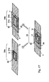
- FIGS. 1A and 1B are perspective view and side view, respectively, of a wireless portable device according to a first embodiment of the present invention.
- FIG. 2 is an exploded perspective view showing the structure of each layer of the printed circuit board of the wireless portable device according to the first embodiment of the present invention.
- FIGS. 3A and 3B are perspective view and side view, respectively, of the equivalent current restriction structure in the wireless portable device according to the first embodiment of the present invention
- FIG. 3C is an exploded perspective view showing the structure of each layer of the printed circuit board.
- FIG. 4 shows first and second current restriction structures in the wireless portable device according to the first embodiment of the present invention.
- FIGS. 5A and 5B are perspective view and side view, respectively, of a wireless portable device according to a second embodiment of the present invention.
- FIG. 6 is an exploded perspective view showing the structure of each layer of the printed circuit board in a wireless portable device according to a second embodiment of the present invention
- FIGS. 7A and 7B are perspective view and side view, respectively, of an equivalent current restriction structure in the wireless portable device according to the second embodiment of the present invention
- FIG. 7C is an exploded perspective view showing the structure of each layer of the printed circuit board.
- FIG. 8 shows first and second current restriction structures in the wireless portable device according to the second embodiment of the present invention.
- FIGS. 9A and 9B are perspective view and side view, respectively, of a wireless portable device according to a third embodiment of the present invention.
- FIG. 10 is an exploded perspective view showing the structure of each layer of the printed circuit board of the wireless portable device according to the third embodiment of the present invention.
- FIGS. 11A and 11B are perspective view and side view, respectively, of a wireless portable device according to a fourth embodiment of the present invention.
- FIG. 12 is an exploded perspective view showing the structure of each layer of the printed circuit board of the wireless portable device according to the fourth embodiment of the present invention.
- FIGS. 13A and 13B are perspective view and side view, respectively, of a wireless portable device according to a fifth embodiment of the present invention.
- FIGS. 14A and 14B are perspective view and side view, respectively, of a wireless portable device according to a sixth embodiment of the present invention.
- FIG. 15 is an exploded perspective view showing the structure of each layer of the printed circuit board in the wireless portable device according to the sixth embodiment of the present invention, with the current restriction structure therein shown at the center.
- FIGS. 16A and 16B are perspective view and side view, respectively, of an equivalent current restriction structure in the wireless portable device according to the sixth embodiment of the present invention
- FIG. 16C is an exploded view showing the structure of each layer.
- FIG. 17 shows the first and second ⁇ -shaped rectangular current restriction structures in the wireless portable device according to the sixth embodiment of the present invention.
- FIG. 18 is a cross-sectional view showing a wireless portable device according to a seventh embodiment of the present invention.
- FIGS. 19A and 19B are perspective view and side view, respectively, of a wireless portable device according to an eighth embodiment of the present invention.
- FIGS. 20A and 20B are perspective view and side view, respectively, of a wireless portable device according to a ninth embodiment of the present invention.
- FIGS. 21A and 21B are perspective view and side view, respectively, of a typical wireless portable device of a prior art
- FIG. 21C is an exploded view showing the structure of each layer of the printed circuit board.
- FIGS. 22A and 22B are respectively a perspective view of the structure restricting the current on a typical cable in the prior art and a sectional view taken on the central plane of the cable.
- Each printed circuit board shown herein is a four-layer circuit board (first layer/signaling layer; second layer/ground layer; third layer/power source layer; and fourth layer/signaling layer), similarly to the structure of the conventional device.
- the space between adjacent layers of the circuit board is filled with a dielectric material such as a glass epoxy material etc., although not specifically depicted.
- the via-hole used herein is such that a conductive layer is formed around an air hole.
- the via-hole penetrating a metallic pattern is thereby connected to the metallic pattern. It is to be noted that aligned positions of the layers at which a via-hole penetrates are provided with holes to be used for the via-holes.
- the wireless portable device of the present embodiment has a configuration wherein, for isolation of a radio circuit block 21 from a digital circuit block 22 , a current restriction structure 1 is mounted between both the circuit blocks disposed in a printed circuit board.
- the current restriction structure 1 includes metallic planes 2 and 3 disposed parallel to the overlying and underlying layers (first layer and third layer) so as to sandwich therebetween the ground layer.
- Arrays of via-holes 5 are formed to extend along straight lines on both lateral sides of the metallic planes (the locations of the metallic planes roughly corresponding to the ends of the printed circuit board as viewed in the direction normal to the direction connecting together the radio circuit block and the digital circuit block), and formed at a location which is apart by desired distances (Lr and Ld) from both the ends of the metallic planes as viewed in the direction connecting together the radio circuit block and the digital circuit block.
- the ground layer 4 is configured to have a width somewhat smaller than the width of a portion of the metallic planes sandwiched between the via-hole arrays. Accordingly, the width of this portion of the metallic planes is somewhat larger than the width of the ground layer.
- Each of these metallic planes is obtained by combining two metallic strips (a metallic strip having a length of Lr and located on the side of radio circuit block, and another metallic strip having a length of Ld and located on the side of the digital circuit block) at the via-hole array as the boundary therebetween, as will be described later.
- the lengths of Lr and LdB of the metallic strips are set at 1 ⁇ 4 of the wavelengths of the subject current to be restricted.
- fr is the frequency of the radio-frequency current (corresponding to a wavelength of ⁇ r) to be restricted from entering the digital circuit block out of the radio circuit block
- fd is the frequency of the higher-harmonic-wave current (corresponding to a wavelength of ⁇ d) to be restricted from entering the radio circuit block out of the digital circuit block
- the via-holes penetrate from the first layer to the third layer, wherein the via-holes disposed Lr apart from one end of the metallic planes (disposed Ld apart from the other end) electrically connect together the overlying and underlying metallic planes and the ground layer.
- the via-holes disposed on both lateral sides of the metallic planes electrically connect together the overlying and underlying metallic planes (without connecting to the ground layer). That the via-holes disposed on both lateral sides of the metallic plane do not connect the ground layer results from the fact that the width of the metallic planes is larger than the ground width at the position and thus the via-holes penetrate the printed circuit board without penetrating the ground layer.
- the spacing between the adjacent via-holes is significantly shorter than the wavelength to be considered, whereby the via-holes are disposed at a narrow pitch or at a high density.
- the current restriction structure 1 can be equivalently expressed by the structure of a rectangular cylindrical metallic tube shown in FIG. 3 , wherein only the current restriction structure is depicted.
- the via-hole array located on both the lateral sides of the metallic planes is equivalently expressed by metallic strips 7 ( 7 a / 7 b ) and 8 ( 8 a / 8 b ) which couple together the overlying and underlying metallic planes.
- the configuration is equivalently such that the ground layer is completely enclosed within the four metallic planes (overlying metallic plane 2 , underlying metallic plane 3 , and both the side metallic planes 7 and 8 ).
- the configuration is such that the ground layer is covered by a rectangular cylindrical metallic tube.
- the via-hole array which is Lr apart from one end of the metallic plane (and at the same time, Ld apart from the other end) is equivalently expressed by a short-circuiting plate 6 ( 6 a and 6 b ) which connects together the overlying and underlying metallic planes and the ground layer.
- such a configuration can be construed as two current restriction units (two rectangular cylindrical metallic tubes) juxtaposed with each other, with the via-hole array (short-circuiting plate 6 ) having the configuration as described above being the boundary. More specifically, as shown in FIG. 4 , the configuration can be construed such that the first current restriction unit 1 a is disposed on the radio circuit block side, whereas the second current restriction unit 1 b is disposed on the digital circuit block side, with the short-circuiting plates 6 configured as the via-hole array being disposed back to back.
- the first current restriction unit 1 a has a configuration wherein the distal end thereof as viewed from the radio circuit block is short-circuited.
- the metallic strips formed as the overlying, underlying and side layers for the ground layer have a length (Lr) equal to 1 ⁇ 4 of the wavelength, ⁇ r, of the subject radio-frequency current in the direction connecting together the radio circuit block and the digital circuit block.
- the current restriction unit has a configuration wherein a transmission line (having a shortcircuited distal end) is formed to enclose therein a ground layer, and the transmission line has a length of ⁇ r/4.
- the input impedance against the radio circuit block is higher at the position of the open plane of the first current restriction unit 1 a .
- the second current restriction unit 1 b has a configuration wherein the distal end thereof as viewed from the digital circuit block is shortcircuited.
- the metallic strips formed as the overlying, underlying and side layers for the ground layer have a length (Ld) equal to 1 ⁇ 4 of the wavelength, ⁇ d, of the subject higher-harmonic-wave current in the direction connecting together the radio circuit block and the digital circuit block.
- Ld length of the wavelength, ⁇ d
- the effect of the current restriction structure is that the higher-harmonic-wave current is restricted from entering the radio circuit block out of the digital circuit block, and the radio-frequency current is restricted from entering the digital circuit block out of the radio circuit block. This suppresses the electromagnetic coupling between the radio circuit block and the digital circuit block, thereby assuring a more excellent quality for the wireless portable device.
- the wireless portable device of the present embodiment is such that only via-hole arrays disposed on both lateral sides of the metallic planes in the wireless portable device of the first embodiment are removed.
- the width of the ground layer is equivalent to that of the circuit board, wherein the via-hole arrays are arranged at a narrow pitch and a high density to penetrate the first through third layers.
- the via-hole array can be construed equivalently as a metallic plate without problem, wherein the current restriction structure 1 can be equivalently expressed by the structure shown in FIG. 7 .
- the current restriction structure 1 is such that the first current restriction unit 1 a is mounted on the side at which the radio circuit block is disposed and the second current restriction unit 1 b is mounted on the side at which the digital circuit block is disposed, with the short-circuiting plates 6 formed by the via-hole array being disposed back to back.
- the principle is same as that of the first embodiment, although there is no metallic strip disposed on both the lateral sides (it is not a “tube” in a strict meaning; however, may constitute a rectangular cylindrical metallic tube in principle). More specifically, due to a higher input impedances at the respective open planes of the first and second current restriction units having lengths of ⁇ r/4 and ⁇ d/4, respectively, measured from the short-circuiting plate 6 , the current generated from one of the circuit blocks is prevented from flowing to the other of the circuit blocks. Thus, the electromagnetic coupling can be suppressed similarly to the first embodiment.
- wireless portable devices capable of suppressing the electromagnetic coupling between the radio circuit block and the digital circuit block.
- FIGS. 9A , 9 B and 10 showing a third embodiment of the present invention
- a wireless portable device of the present embodiment only a higher-harmonic-wave current entering the radio circuit block from the digital circuit block is noticed, and is restricted.
- These figures show a wireless portable device mounting thereon a current restriction structure for restricting the higher-harmonic-wave current from entering the radio circuit block out of the digital circuit block.
- the present embodiment has a configuration wherein only the second current restriction unit of the first embodiment is mounted, a single equivalent rectangular cylindrical metallic tube is provided, and a U-shape via-hole array is formed.
- the wireless portable device may mount thereon a current restriction structure for restricting the radio-frequency current from entering the digital circuit block out of the radio circuit block ( FIGS. 11A , 11 B and 12 ).
- the present embodiment has a configuration wherein only the first current restriction unit of the first embodiment is mounted, a single equivalent rectangular cylindrical metallic tube is provided, and a U-shape via-hole array is formed.
- the third and fourth embodiments have similar advantages for suppressing the electromagnetic coupling (in one direction).
- the via-hole array described therein has a single row.
- the wireless portable device of the present embodiment has a configuration wherein the via-hole array used in the second embodiment, for example, is arranged at a narrow pitch, in a cyclic manner and in a plurality of rows.
- Such a configuration allows enforcement of the connection of the overlying metallic plane 2 , underlying metallic plane 3 and the ground layer 4 (physical enforcement of the connection).
- a plurality of metallic plates are equivalently disposed therein, the function of the short-circuiting plate is more effective.
- each of the via-hole arrays disposed on the lateral sides of the metallic planes may be arranged at a narrow pitch, in a cyclic manner, and in a plurality of rows.
- the connection between the metallic plane 2 overlying the ground layer and the metallic plane 3 underlying the ground layer can be enforced.
- each of some or all of the via-hole arrays may be arranged in a plurality of rows.
- one of the outermost rows among a plurality of rows of the via-hole array is disposed on the location of the metallic plane apart from the end thereof in the direction of a line passing through the radio circuit block and the digital circuit block by 1 ⁇ 4 of the wavelength of the subject current to be restricted.
- the length of the metallic plane is increased in the direction by the width of the plurality of rows of the via-hole array.
- Such a configuration wherein the via-hole array has a plurality of rows can be also employed in the embodiments to follow.
- the digital circuit block is disposed in the vicinity of the center of the printed circuit board for the sake of convenience.
- the wireless portable device of the present embodiment has a configuration wherein a ⁇ -shaped current restriction structure 34 is mounted on the circumference of the digital circuit block. This corresponds to the configuration wherein the current restriction structure 1 described in connection with the first through fifth embodiments is disposed to encircle the digital circuit block 22 , and the basic structures thereof such as the film structure are similar to those of those embodiments.
- the ⁇ -shaped metallic planes are disposed parallel to the overlying and underlying layers (first layer and third layer) to sandwich therebetween the ground layer.
- Each of the metallic planes is configured to a pattern having therein an opening, which is somewhat larger than the size of the periphery of the digital circuit block, and having a widthwise length of Lr+Ld as in the cases of the above embodiments.
- the via-hole array is disposed apart from the inner edge of the metallic plane by a desired distance (Ld) to form a ⁇ -shape, wherein individual via-holes penetrate from the first layer to the third layer.
- the via-hole array can be construed as a metallic plate also in this case.
- the ⁇ -shaped via-hole array is located at a distance of Ld apart from the inner edge of the metallic plane and at a distanced of Lr apart from the outer edge thereof, whereby these lengths are set at 1 ⁇ 4 of the wavelengths of the subject currents to be restricted.
- FIGS. 16A to 16C and 17 show the ⁇ -shaped current restriction structure 34 wherein the via-hole array is equivalently construed as a metallic plate.
- FIG. 17 illustrates the ⁇ -shaped first and second current restriction units in the present embodiment. As shown in these figures, this can be construed as a structure of two lopped current restriction units mounted, wherein the ⁇ -shaped short-circuiting plates 31 ( 31 a and 31 b ) implemented by the via-hole array are disposed back to back.
- the first ⁇ -shaped current restriction unit 34 a is mounted on the inner side (the side at which the digital circuit block is mounted) of the via-hole array constituting a boundary, and is implemented by ⁇ -shaped metallic planes ( 32 and 33 ) each having a short-circuited distal end and a widthwise length, Ld, equal to 1 ⁇ 4 of the wavelength ⁇ d of the subject higher-harmonic-wave current.
- the ⁇ -shaped second current restriction unit 34 b is mounted on the outer side, and is implemented by ⁇ -shaped metallic planes ( 32 and 33 ) each having a short-circuited distal end and a widthwise length, Lr, equal to 1 ⁇ 4 of the wavelength ⁇ r of the subject radio-frequency current.
- the ⁇ -shaped first current restriction unit 34 a as disposed to surround the digital circuit block 22 and having a higher impedance at the open plane directed inwardly, can suppress the higher-harmonic-wave current from flowing out of the digital circuit block to the circumference thereof.
- entering of the higher-harmonic-wave current to the radio circuit block for example, can be restricted, thereby suppressing the electromagnetic coupling.
- the ⁇ -shaped second current restriction unit 34 b has an open plane directed outwardly. Accordingly, entering of the current to the digital circuit block from nearby circuit blocks etc. is restricted, thereby suppressing the electromagnetic coupling.
- the shape of the current restriction structure is inadequate to be referred to as “tube”, the advantage of the rectangular cylindrical metallic tube in the present embodiment is basically similar to those of the above embodiments.
- the current restriction units are disposed between the circuit blocks which is may involve an electromagnetic coupling therebetween, having an effect on the current flowing into the ground layer of the printed circuit board.
- the ⁇ -shaped current restriction structure is disposed to surround the location at which the current is generated (the circuit block surrounded may be either a digital circuit block as in the present embodiment or a radio circuit block).
- the present embodiment has the advantage of restricting the current, which may possibly cause the electromagnetic coupling, from flowing onto the printed circuit board.
- a printed circuit board may have eight layers or sixteen layers, for example, other than the four layers in the wireless portable device of the present invention, although the four-layer circuit boards are exemplified heretofore.
- the metallic planes ( 2 and 3 ) formed to overlie and underlie the ground layer are included in the signaling layer and the power source layer (first layer and third layer), respectively, independent layers having the metallic planes may be provided separately from these layers. Or else, it is possible to employ a configuration wherein either one of the overlying and underlying metallic planes is included in the signaling layer or the power source layer.
- the overlying and underlying metallic planes are formed respectively on first layers, when numbered from the ground layer, in the wireless portable device of the present embodiment; however, the layers having the metallic planes may be disposed in any of the layers so long as these layers overlie and underlie the ground layer.
- the overlying metallic plane may be formed on the (N ⁇ 3)-th layer and the underlying metallic plane may be formed on the N-th layer, assuming that the ground layer resides on the (N ⁇ 1)-th layer etc.
- the package casings for the wireless portable devices may be made of a metallic material, although most of them are made of a nonmetallic material such as plastics or resin.
- a current which may possibly cause the electromagnetic coupling may flow on the surface of the package casing.
- the current restriction structure of the present invention may be applied to the casing 52 , assuming that the metallic package casing 52 is an equivalent ground layer.
- This structure may be such that the rectangular cylindrical metallic tube covers the metallic package casing for substantially complete enclosure thereof, and a short-circuiting plate is connected thereto for short-circuiting together the metallic package casing and the rectangular cylindrical tube at the position Lr apart from one end of the rectangular cylindrical metallic tube (or Ld apart from the other end thereof).
- this configuration corresponds to the configuration wherein the current restriction structure implemented by the metallic plate shown in FIG. 3 is applied to the metallic package casing 52 .
- the ground layer shown in FIG. 3 is replaced by the metallic package casing 52 . Accordingly, the advantage is similar to those in the embodiments described heretofore, whereby the electromagnetic coupling caused by the current on the package casing can be suppressed.
- the wireless portable device of the present embodiment is such that the current restriction structure in the second embodiment is applied to a metallic package casing for the case using the metallic package casing 52 as well. Also in this case, only the ground layer is replaced by the metallic package casing.
- the advantage is similar to those in the embodiments described heretofore.
- the length of the metallic strip of the current restriction structure is equal to 1 ⁇ 4 of the wavelength of the subject current.
- a magnetic member 50 or an insulator member 50
- the present invention is not limited to application to the wireless portable device such as portable cellular phone and personal data assistant, and may be applied to general electronic or electric appliances.
- a magnetic coupling may occur between a digital circuit block and an analog circuit block (corresponding to the radio circuit block in the present invention).
- the present invention if applied to such a case, has a similar advantage.
- the current restriction structure restricts the higher-harmonic-wave current from entering the radio circuit block out of the digital circuit block, and the radio-frequency current from entering the digital circuit block out of the radio circuit block, the electromagnetic coupling between the digital circuit block and the radio circuit block can be suppressed to assure a higher quality.
Abstract
Description
Lr=λr/4=(c 0 /fr)/4 (1), and
Ld=λd/4=(c 0 /fd)/4 (2),
wherein co is the velocity of light (3×10⁸ m/s).
As depicted, the via-holes penetrate from the first layer to the third layer, wherein the via-holes disposed Lr apart from one end of the metallic planes (disposed Ld apart from the other end) electrically connect together the overlying and underlying metallic planes and the ground layer. In addition, the via-holes disposed on both lateral sides of the metallic planes electrically connect together the overlying and underlying metallic planes (without connecting to the ground layer). That the via-holes disposed on both lateral sides of the metallic plane do not connect the ground layer results from the fact that the width of the metallic planes is larger than the ground width at the position and thus the via-holes penetrate the printed circuit board without penetrating the ground layer.
Claims (16)
Applications Claiming Priority (3)
| Application Number | Priority Date | Filing Date | Title |
|---|---|---|---|
| JP2001-114391 | 2001-04-12 | ||
| JP2001114391A JP3531621B2 (en) | 2001-04-12 | 2001-04-12 | Portable wireless devices |
| PCT/JP2002/003586 WO2002084784A1 (en) | 2001-04-12 | 2002-04-10 | Mobile radio-utilizing device |
Publications (2)
| Publication Number | Publication Date |
|---|---|
| US20040127249A1 US20040127249A1 (en) | 2004-07-01 |
| US7164898B2 true US7164898B2 (en) | 2007-01-16 |
Family
ID=18965475
Family Applications (1)
| Application Number | Title | Priority Date | Filing Date |
|---|---|---|---|
| US10/474,756 Expired - Fee Related US7164898B2 (en) | 2001-04-12 | 2002-04-10 | Wireless portable device |
Country Status (4)
| Country | Link |
|---|---|
| US (1) | US7164898B2 (en) |
| EP (1) | EP1403960A1 (en) |
| JP (1) | JP3531621B2 (en) |
| WO (1) | WO2002084784A1 (en) |
Cited By (12)
| Publication number | Priority date | Publication date | Assignee | Title |
|---|---|---|---|---|
| US20050192068A1 (en) * | 2004-01-22 | 2005-09-01 | Josef Fenk | Radio frequency arrangement and production method and also use |
| US20060232491A1 (en) * | 2005-04-18 | 2006-10-19 | Anritsu Corporation | Electromagnetic wave shield box |
| US20090134863A1 (en) * | 2007-11-27 | 2009-05-28 | Kabushiki Kaisha Toshiba | Electricity meter |
| US20100289619A1 (en) * | 2009-05-13 | 2010-11-18 | Kabushiki Kaisha Tokai Rika Denki Seisakusho | Antenna device |
| US20130003321A1 (en) * | 2010-03-15 | 2013-01-03 | Nec Corporation | Noise suppression structure |
| US20130015926A1 (en) * | 2010-03-30 | 2013-01-17 | Nec Corporation | Noise suppression structure |
| US20130069836A1 (en) * | 2011-09-21 | 2013-03-21 | Sony Mobile Communications Japan, Inc. | Wireless communication apparatus |
| US20150364804A1 (en) * | 2014-06-13 | 2015-12-17 | Freescale Semiconductor, Inc. | Radio frequency coupling structure |
| US20160135300A1 (en) * | 2013-06-28 | 2016-05-12 | Canon Kabushiki Kaisha | Printed circuit board |
| US9887449B2 (en) | 2014-08-29 | 2018-02-06 | Nxp Usa, Inc. | Radio frequency coupling structure and a method of manufacturing thereof |
| US10103447B2 (en) | 2014-06-13 | 2018-10-16 | Nxp Usa, Inc. | Integrated circuit package with radio frequency coupling structure |
| US10225925B2 (en) | 2014-08-29 | 2019-03-05 | Nxp Usa, Inc. | Radio frequency coupling and transition structure |
Families Citing this family (15)
| Publication number | Priority date | Publication date | Assignee | Title |
|---|---|---|---|---|
| AU2003259016A1 (en) * | 2002-10-03 | 2004-04-23 | Amplus Communication Pte Ltd | Radio frequency transceivers |
| JP2004363392A (en) * | 2003-06-05 | 2004-12-24 | Hitachi Ltd | Printed wiring board and radio communication apparatus |
| US7456792B2 (en) | 2004-02-26 | 2008-11-25 | Fractus, S.A. | Handset with electromagnetic bra |
| EP1771919A1 (en) | 2004-07-23 | 2007-04-11 | Fractus, S.A. | Antenna in package with reduced electromagnetic interaction with on chip elements |
| US7376408B2 (en) | 2004-08-10 | 2008-05-20 | Sony Ericsson Mobile Communications Ab | Reduction of near field electro-magnetic scattering using high impedance metallization terminations |
| WO2007039071A2 (en) | 2005-09-19 | 2007-04-12 | Fractus, S.A. | Antenna set, portable wireless device, and use of a conductive element for tuning the ground-plane of the antenna set |
| US9723709B2 (en) * | 2007-10-22 | 2017-08-01 | Todd Steigerwald | Method for assigning control channels |
| WO2011115094A1 (en) * | 2010-03-15 | 2011-09-22 | 日本電気株式会社 | Noise suppression structure |
| JP5172925B2 (en) * | 2010-09-24 | 2013-03-27 | 株式会社東芝 | Wireless device |
| JP4858733B1 (en) * | 2010-10-06 | 2012-01-18 | 横浜ゴム株式会社 | Transmitter |
| ES2447298T3 (en) | 2011-03-24 | 2014-03-11 | Alcatel Lucent | Diplexer circuit and manufacturing procedure of a printed circuit board for it |
| EP2508839B1 (en) * | 2011-04-07 | 2014-07-09 | Carl Mahr Holding GmbH | Measuring device with transmission circuit for wireless transmission of a measurement value transmission signal |
| TW201351175A (en) * | 2012-06-01 | 2013-12-16 | Wistron Corp | Circuit layout method for printed circuit board, eletronic device and computer readable recording media |
| WO2014027457A1 (en) * | 2012-08-15 | 2014-02-20 | 日本電気株式会社 | Current suppression element and current suppression method |
| KR102176368B1 (en) * | 2015-01-05 | 2020-11-09 | 엘지전자 주식회사 | Antenna module and mobile terminal having the same |
Citations (9)
| Publication number | Priority date | Publication date | Assignee | Title |
|---|---|---|---|---|
| US5453713A (en) * | 1992-07-06 | 1995-09-26 | Digital Equipment Corporation | Noise-free analog islands in digital integrated circuits |
| JPH08321720A (en) | 1995-05-26 | 1996-12-03 | Fujitsu Ltd | Voltage controlled oscillator |
| JPH0918205A (en) | 1995-06-27 | 1997-01-17 | Toshiba Corp | Microwave circuit |
| JPH11274818A (en) | 1998-03-20 | 1999-10-08 | Fujitsu Ltd | High frequency circuit device |
| US6121827A (en) * | 1999-04-15 | 2000-09-19 | Lucent Technologies, Inc. | Digital noise reduction in integrated circuits and circuit assemblies |
| US6166457A (en) * | 1996-10-07 | 2000-12-26 | Fuji Xerox Co., Ltd. | Printed-circuit assembly |
| US6194913B1 (en) * | 1997-12-22 | 2001-02-27 | Alcatel | Output circuit for digital integrated circuit devices |
| US6335866B1 (en) * | 1997-10-09 | 2002-01-01 | Canon Kabushiki Kaisha | Printed wiring board unit for use with electronic apparatus |
| US6469259B2 (en) * | 2000-02-29 | 2002-10-22 | Kyocera Corporation | Wiring board |
-
2001
- 2001-04-12 JP JP2001114391A patent/JP3531621B2/en not_active Expired - Fee Related
-
2002
- 2002-04-10 WO PCT/JP2002/003586 patent/WO2002084784A1/en not_active Application Discontinuation
- 2002-04-10 EP EP20020718524 patent/EP1403960A1/en not_active Withdrawn
- 2002-04-10 US US10/474,756 patent/US7164898B2/en not_active Expired - Fee Related
Patent Citations (9)
| Publication number | Priority date | Publication date | Assignee | Title |
|---|---|---|---|---|
| US5453713A (en) * | 1992-07-06 | 1995-09-26 | Digital Equipment Corporation | Noise-free analog islands in digital integrated circuits |
| JPH08321720A (en) | 1995-05-26 | 1996-12-03 | Fujitsu Ltd | Voltage controlled oscillator |
| JPH0918205A (en) | 1995-06-27 | 1997-01-17 | Toshiba Corp | Microwave circuit |
| US6166457A (en) * | 1996-10-07 | 2000-12-26 | Fuji Xerox Co., Ltd. | Printed-circuit assembly |
| US6335866B1 (en) * | 1997-10-09 | 2002-01-01 | Canon Kabushiki Kaisha | Printed wiring board unit for use with electronic apparatus |
| US6194913B1 (en) * | 1997-12-22 | 2001-02-27 | Alcatel | Output circuit for digital integrated circuit devices |
| JPH11274818A (en) | 1998-03-20 | 1999-10-08 | Fujitsu Ltd | High frequency circuit device |
| US6121827A (en) * | 1999-04-15 | 2000-09-19 | Lucent Technologies, Inc. | Digital noise reduction in integrated circuits and circuit assemblies |
| US6469259B2 (en) * | 2000-02-29 | 2002-10-22 | Kyocera Corporation | Wiring board |
Cited By (20)
| Publication number | Priority date | Publication date | Assignee | Title |
|---|---|---|---|---|
| US20050192068A1 (en) * | 2004-01-22 | 2005-09-01 | Josef Fenk | Radio frequency arrangement and production method and also use |
| US7349724B2 (en) * | 2004-01-22 | 2008-03-25 | Infineon Technologies Ag | Radio frequency arrangement and production method and also use |
| US20060232491A1 (en) * | 2005-04-18 | 2006-10-19 | Anritsu Corporation | Electromagnetic wave shield box |
| US7512430B2 (en) * | 2005-04-18 | 2009-03-31 | Anritsu Corporation | Electromagnetic wave shield box |
| US20090134863A1 (en) * | 2007-11-27 | 2009-05-28 | Kabushiki Kaisha Toshiba | Electricity meter |
| US7919960B2 (en) * | 2007-11-27 | 2011-04-05 | Toshiba Toko Meter Systems Co., Ltd. | Electricity meter capable of minimizing the risk of data destruction from lightning or surge |
| US20100289619A1 (en) * | 2009-05-13 | 2010-11-18 | Kabushiki Kaisha Tokai Rika Denki Seisakusho | Antenna device |
| US20130003321A1 (en) * | 2010-03-15 | 2013-01-03 | Nec Corporation | Noise suppression structure |
| US20130015926A1 (en) * | 2010-03-30 | 2013-01-17 | Nec Corporation | Noise suppression structure |
| US9225049B2 (en) * | 2010-03-30 | 2015-12-29 | Nec Corporation | Noise suppression structure |
| US9088069B2 (en) * | 2011-09-21 | 2015-07-21 | Sony Corporation | Wireless communication apparatus |
| US20130069836A1 (en) * | 2011-09-21 | 2013-03-21 | Sony Mobile Communications Japan, Inc. | Wireless communication apparatus |
| US20160135300A1 (en) * | 2013-06-28 | 2016-05-12 | Canon Kabushiki Kaisha | Printed circuit board |
| US10251274B2 (en) * | 2013-06-28 | 2019-04-02 | Canon Kabushiki Kaisha | Printed circuit board |
| US10721821B2 (en) | 2013-06-28 | 2020-07-21 | Canon Kabushiki Kaisha | Printed circuit board |
| US20150364804A1 (en) * | 2014-06-13 | 2015-12-17 | Freescale Semiconductor, Inc. | Radio frequency coupling structure |
| US9620841B2 (en) * | 2014-06-13 | 2017-04-11 | Nxp Usa, Inc. | Radio frequency coupling structure |
| US10103447B2 (en) | 2014-06-13 | 2018-10-16 | Nxp Usa, Inc. | Integrated circuit package with radio frequency coupling structure |
| US9887449B2 (en) | 2014-08-29 | 2018-02-06 | Nxp Usa, Inc. | Radio frequency coupling structure and a method of manufacturing thereof |
| US10225925B2 (en) | 2014-08-29 | 2019-03-05 | Nxp Usa, Inc. | Radio frequency coupling and transition structure |
Also Published As
| Publication number | Publication date |
|---|---|
| EP1403960A1 (en) | 2004-03-31 |
| JP2002314491A (en) | 2002-10-25 |
| WO2002084784A1 (en) | 2002-10-24 |
| US20040127249A1 (en) | 2004-07-01 |
| JP3531621B2 (en) | 2004-05-31 |
Similar Documents
| Publication | Publication Date | Title |
|---|---|---|
| US7164898B2 (en) | Wireless portable device | |
| KR100733103B1 (en) | Embedded rf vertical interconnect for flexible conformal antenna | |
| JP2867985B2 (en) | Printed circuit board | |
| US7528796B2 (en) | Antenna system | |
| US6232849B1 (en) | RF waveguide signal transition apparatus | |
| CA2177746C (en) | Antenna device and communication apparatus incorporating the same | |
| TW201640735A (en) | Radio frequency connection arrangement | |
| US20040070538A1 (en) | Antenna incorporating filter | |
| CN102593565B (en) | The input and output connecting structure of dielectric-filled waveguide | |
| CN101300717A (en) | Mobile communication device and an antenna assembly for the device | |
| CN110798962B (en) | Printed circuit board, optical module and optical transmission apparatus | |
| US11659658B2 (en) | Multilayer board | |
| JPH1188209A (en) | Mobile communication equipment | |
| US20110122041A1 (en) | Planar antenna | |
| JPH10261914A (en) | Antenna device | |
| US20140299374A1 (en) | Flat cable | |
| US6178311B1 (en) | Method and apparatus for isolating high frequency signals in a printed circuit board | |
| CN100472676C (en) | Distribution capacitor in high density application | |
| CN113161719A (en) | Printed circuit board for base station antenna | |
| JP6949640B2 (en) | Array antenna board | |
| JP3803976B2 (en) | Electronic device for wireless signal transmission | |
| US20210066775A1 (en) | Multilayer board and electronic device | |
| EP3909095B1 (en) | Cooling in a waveguide arrangement | |
| US20060097932A1 (en) | Small size thin type antenna, multilayered substrate, high frequency module, and radio terminal mounting them | |
| JP3824998B2 (en) | Dielectric waveguide antenna |
Legal Events
| Date | Code | Title | Description |
|---|---|---|---|
| AS | Assignment |
Owner name: NEC CORPORATION, JAPAN Free format text: ASSIGNMENT OF ASSIGNORS INTEREST;ASSIGNORS:HANKUI, EIJI;KURIYAMA, TOSHIHIDE;REEL/FRAME:015053/0059 Effective date: 20031008 |
|
| FEPP | Fee payment procedure |
Free format text: PAYOR NUMBER ASSIGNED (ORIGINAL EVENT CODE: ASPN); ENTITY STATUS OF PATENT OWNER: LARGE ENTITY |
|
| CC | Certificate of correction | ||
| CC | Certificate of correction | ||
| FPAY | Fee payment |
Year of fee payment: 4 |
|
| FPAY | Fee payment |
Year of fee payment: 8 |
|
| AS | Assignment |
Owner name: LENOVO INNOVATIONS LIMITED (HONG KONG), HONG KONG Free format text: ASSIGNMENT OF ASSIGNORS INTEREST;ASSIGNOR:NEC CORPORATION;REEL/FRAME:033720/0767 Effective date: 20140618 |
|
| FEPP | Fee payment procedure |
Free format text: MAINTENANCE FEE REMINDER MAILED (ORIGINAL EVENT CODE: REM.); ENTITY STATUS OF PATENT OWNER: LARGE ENTITY |
|
| LAPS | Lapse for failure to pay maintenance fees |
Free format text: PATENT EXPIRED FOR FAILURE TO PAY MAINTENANCE FEES (ORIGINAL EVENT CODE: EXP.); ENTITY STATUS OF PATENT OWNER: LARGE ENTITY |
|
| STCH | Information on status: patent discontinuation |
Free format text: PATENT EXPIRED DUE TO NONPAYMENT OF MAINTENANCE FEES UNDER 37 CFR 1.362 |
|
| FP | Lapsed due to failure to pay maintenance fee |
Effective date: 20190116 |