US7167613B2 - Interlaced array of piano MEMs micromirrors - Google Patents
Interlaced array of piano MEMs micromirrors Download PDFInfo
- Publication number
- US7167613B2 US7167613B2 US11/075,650 US7565005A US7167613B2 US 7167613 B2 US7167613 B2 US 7167613B2 US 7565005 A US7565005 A US 7565005A US 7167613 B2 US7167613 B2 US 7167613B2
- Authority
- US
- United States
- Prior art keywords
- pivoting members
- lateral axis
- pivoting
- array
- substrate
- Prior art date
- Legal status (The legal status is an assumption and is not a legal conclusion. Google has not performed a legal analysis and makes no representation as to the accuracy of the status listed.)
- Expired - Lifetime, expires
Links
- 239000000758 substrate Substances 0.000 claims description 40
- 230000003247 decreasing effect Effects 0.000 claims description 7
- 239000000463 material Substances 0.000 claims description 3
- 230000003287 optical effect Effects 0.000 abstract description 9
- WYTGDNHDOZPMIW-RCBQFDQVSA-N alstonine Natural products C1=CC2=C3C=CC=CC3=NC2=C2N1C[C@H]1[C@H](C)OC=C(C(=O)OC)[C@H]1C2 WYTGDNHDOZPMIW-RCBQFDQVSA-N 0.000 description 13
- 230000010287 polarization Effects 0.000 description 6
- 239000011295 pitch Substances 0.000 description 5
- 230000004913 activation Effects 0.000 description 4
- 238000003491 array Methods 0.000 description 4
- 239000013078 crystal Substances 0.000 description 3
- 238000010586 diagram Methods 0.000 description 3
- 230000005684 electric field Effects 0.000 description 3
- 238000004519 manufacturing process Methods 0.000 description 3
- 238000000708 deep reactive-ion etching Methods 0.000 description 2
- 238000000034 method Methods 0.000 description 2
- 230000003595 spectral effect Effects 0.000 description 2
- 241001156002 Anthonomus pomorum Species 0.000 description 1
- 230000005540 biological transmission Effects 0.000 description 1
- 239000011248 coating agent Substances 0.000 description 1
- 238000000576 coating method Methods 0.000 description 1
- 238000010276 construction Methods 0.000 description 1
- 230000007423 decrease Effects 0.000 description 1
- 230000006866 deterioration Effects 0.000 description 1
- 230000009977 dual effect Effects 0.000 description 1
- 230000000694 effects Effects 0.000 description 1
- 230000005686 electrostatic field Effects 0.000 description 1
- 239000000835 fiber Substances 0.000 description 1
- PCHJSUWPFVWCPO-UHFFFAOYSA-N gold Chemical compound [Au] PCHJSUWPFVWCPO-UHFFFAOYSA-N 0.000 description 1
- 239000010931 gold Substances 0.000 description 1
- 229910052737 gold Inorganic materials 0.000 description 1
- 238000002955 isolation Methods 0.000 description 1
- 230000006798 recombination Effects 0.000 description 1
- 238000005215 recombination Methods 0.000 description 1
- 238000000926 separation method Methods 0.000 description 1
- 230000001052 transient effect Effects 0.000 description 1
- 239000002023 wood Substances 0.000 description 1
Images


Classifications
-
- B—PERFORMING OPERATIONS; TRANSPORTING
- B81—MICROSTRUCTURAL TECHNOLOGY
- B81B—MICROSTRUCTURAL DEVICES OR SYSTEMS, e.g. MICROMECHANICAL DEVICES
- B81B3/00—Devices comprising flexible or deformable elements, e.g. comprising elastic tongues or membranes
- B81B3/0062—Devices moving in two or more dimensions, i.e. having special features which allow movement in more than one dimension
-
- G—PHYSICS
- G02—OPTICS
- G02B—OPTICAL ELEMENTS, SYSTEMS OR APPARATUS
- G02B26/00—Optical devices or arrangements for the control of light using movable or deformable optical elements
- G02B26/08—Optical devices or arrangements for the control of light using movable or deformable optical elements for controlling the direction of light
- G02B26/0816—Optical devices or arrangements for the control of light using movable or deformable optical elements for controlling the direction of light by means of one or more reflecting elements
- G02B26/0833—Optical devices or arrangements for the control of light using movable or deformable optical elements for controlling the direction of light by means of one or more reflecting elements the reflecting element being a micromechanical device, e.g. a MEMS mirror, DMD
- G02B26/0841—Optical devices or arrangements for the control of light using movable or deformable optical elements for controlling the direction of light by means of one or more reflecting elements the reflecting element being a micromechanical device, e.g. a MEMS mirror, DMD the reflecting element being moved or deformed by electrostatic means
-
- G—PHYSICS
- G02—OPTICS
- G02B—OPTICAL ELEMENTS, SYSTEMS OR APPARATUS
- G02B6/00—Light guides; Structural details of arrangements comprising light guides and other optical elements, e.g. couplings
- G02B6/24—Coupling light guides
- G02B6/26—Optical coupling means
- G02B6/35—Optical coupling means having switching means
- G02B6/3564—Mechanical details of the actuation mechanism associated with the moving element or mounting mechanism details
- G02B6/3584—Mechanical details of the actuation mechanism associated with the moving element or mounting mechanism details constructional details of an associated actuator having a MEMS construction, i.e. constructed using semiconductor technology such as etching
-
- B—PERFORMING OPERATIONS; TRANSPORTING
- B81—MICROSTRUCTURAL TECHNOLOGY
- B81B—MICROSTRUCTURAL DEVICES OR SYSTEMS, e.g. MICROMECHANICAL DEVICES
- B81B2201/00—Specific applications of microelectromechanical systems
- B81B2201/04—Optical MEMS
- B81B2201/042—Micromirrors, not used as optical switches
-
- G—PHYSICS
- G02—OPTICS
- G02B—OPTICAL ELEMENTS, SYSTEMS OR APPARATUS
- G02B6/00—Light guides; Structural details of arrangements comprising light guides and other optical elements, e.g. couplings
- G02B6/24—Coupling light guides
- G02B6/26—Optical coupling means
- G02B6/35—Optical coupling means having switching means
- G02B6/351—Optical coupling means having switching means involving stationary waveguides with moving interposed optical elements
- G02B6/3512—Optical coupling means having switching means involving stationary waveguides with moving interposed optical elements the optical element being reflective, e.g. mirror
- G02B6/3518—Optical coupling means having switching means involving stationary waveguides with moving interposed optical elements the optical element being reflective, e.g. mirror the reflective optical element being an intrinsic part of a MEMS device, i.e. fabricated together with the MEMS device
-
- G—PHYSICS
- G02—OPTICS
- G02B—OPTICAL ELEMENTS, SYSTEMS OR APPARATUS
- G02B6/00—Light guides; Structural details of arrangements comprising light guides and other optical elements, e.g. couplings
- G02B6/24—Coupling light guides
- G02B6/26—Optical coupling means
- G02B6/35—Optical coupling means having switching means
- G02B6/354—Switching arrangements, i.e. number of input/output ports and interconnection types
- G02B6/3544—2D constellations, i.e. with switching elements and switched beams located in a plane
-
- G—PHYSICS
- G02—OPTICS
- G02B—OPTICAL ELEMENTS, SYSTEMS OR APPARATUS
- G02B6/00—Light guides; Structural details of arrangements comprising light guides and other optical elements, e.g. couplings
- G02B6/24—Coupling light guides
- G02B6/26—Optical coupling means
- G02B6/35—Optical coupling means having switching means
- G02B6/354—Switching arrangements, i.e. number of input/output ports and interconnection types
- G02B6/356—Switching arrangements, i.e. number of input/output ports and interconnection types in an optical cross-connect device, e.g. routing and switching aspects of interconnecting different paths propagating different wavelengths to (re)configure the various input and output links
-
- G—PHYSICS
- G02—OPTICS
- G02B—OPTICAL ELEMENTS, SYSTEMS OR APPARATUS
- G02B6/00—Light guides; Structural details of arrangements comprising light guides and other optical elements, e.g. couplings
- G02B6/24—Coupling light guides
- G02B6/26—Optical coupling means
- G02B6/35—Optical coupling means having switching means
- G02B6/3564—Mechanical details of the actuation mechanism associated with the moving element or mounting mechanism details
- G02B6/3568—Mechanical details of the actuation mechanism associated with the moving element or mounting mechanism details characterised by the actuating force
- G02B6/357—Electrostatic force
-
- Y—GENERAL TAGGING OF NEW TECHNOLOGICAL DEVELOPMENTS; GENERAL TAGGING OF CROSS-SECTIONAL TECHNOLOGIES SPANNING OVER SEVERAL SECTIONS OF THE IPC; TECHNICAL SUBJECTS COVERED BY FORMER USPC CROSS-REFERENCE ART COLLECTIONS [XRACs] AND DIGESTS
- Y10—TECHNICAL SUBJECTS COVERED BY FORMER USPC
- Y10S—TECHNICAL SUBJECTS COVERED BY FORMER USPC CROSS-REFERENCE ART COLLECTIONS [XRACs] AND DIGESTS
- Y10S359/00—Optical: systems and elements
- Y10S359/904—Micromirror
Definitions
- the present invention relates to a micro-electro-mechanical (MEMs) mirror device for use in an optical switch, and in particular to an interlaced arrays of MEMs mirrors providing minimal electrical cross talk between mirrors.
- MEMs micro-electro-mechanical
- MEMs mirrors for use in optical switches such as the one disclosed in U.S. Pat. No. 6,535,319 issued Mar. 18, 2003 to Buzzetta et al, to redirect beams of light to one of a plurality of output ports include an electro-statically controlled mirror pivotable about a single axis.
- Tilting MEMs mirrors such as the ones disclosed in U.S. Pat. No. 6,491,404 issued Dec. 10, 2002 in the name of Edward Hill, and U.S. Patent Publication No. 2003/0052569, published Mar.
- FIG. 1 The MEMs mirror device, disclosed in the aforementioned Hill patent, is illustrated in FIG. 1 , and includes a rectangular planar surface 2 pivotally mounted by torsional hinges 4 and 5 to anchor posts 7 and 8 , respectively, above a substrate 9 .
- the torsional hinges may take the form of serpentine hinges, which are disclosed in U.S. Pat. No. 6,327,855 issued Dec. 11, 2001 in the name of Hill et al, and in U.S. Patent Publication No. 2002/0126455 published Sep. 12, 2002 in the name of Robert Wood, which are incorporated herein by reference.
- fill factor width/pitch
- this mirror construction restraint greatly restricts other design choices that have to be made in building the overall switch.
- the mirror 1 positioned on the planar surface 2 can be rotated through positive and negative angles, e.g. ⁇ 2 °, by attracting one side 10 a or the other side 10 b of the planar surface 2 to the substrate 6 .
- the intermediate ports receive light for fractions of a millisecond as the mirror 1 sweeps the optical beam past these ports, thereby causing undesirable optical transient or dynamic cross-talk.
- FIG. 2 An example of a MEMs mirror device pivotable about two axes is illustrated in FIG. 2 , and includes a mirror platform 11 pivotally mounted by a first pair of torsion springs 12 and 13 to an external gimbal ring 14 , which is in turn pivotally mounted to a substrate 16 by a second pair of torsion springs 17 and 18 .
- Examples of external gimbal devices are disclosed in U.S. Pat. No. 6,529,652 issued Mar. 4, 2003 to Brenner, and U.S. Pat. No. 6,454,421 issued Sep. 24, 2002 to Yu et al.
- an external gimbal ring greatly limits the number of mirrors that can be arranged in a given area and the relative proximity thereof, i.e. the fill factor. Moreover, the external gimbal ring may cause unwanted reflections from light reflecting off the support frame. These references also require at least four electrodes to actuate each mirror.
- An object of the present invention is to overcome the shortcomings of the prior art by providing two interlaced arrays of MEMs mirror devices, the mirrors in each array being pivotable about different parrallel axes, thereby increasing the spacing between electrodes and minimizing electrical cross-talk.
- the present invention relates to a micro-electro-mechanical device
- a micro-electro-mechanical device mounted on a substrate comprising:
- first pivoting members pivotally mounted on said substrate about a first lateral axis, each of said first pivoting members including a first and a second supporting region on opposite sides of said first lateral axis;
- each of said second pivoting members including a first supporting region interleaved with the first supporting regions of the first array of pivoting members between said first and second lateral axes, and a second supporting region on an opposite side of the second lateral axis;
- a first electrode beneath each of the second supporting region for pivoting the first and second pivoting members about the first axis from a rest position.
- FIG. 1 is an isometric view of a conventional tilting MEMs mirror device
- FIG. 2 is a plan view of a pair of conventional external gimbal ring MEMs mirror devices
- FIG. 3 is an isometric view of a plurality of Piano-MEMs mirror devices
- FIG. 4 is an isometric view of a hinge structure of the mirror devices of FIG. 3 ;
- FIG. 5 is an isometric view of an electrode structure of the mirror devices of FIG. 3 ;
- FIG. 6 is an isometric view of a plurality of Piano-MEMs mirror devices according to an alternative embodiment of the present invention with electrode shields, light redirecting cusps, and a raised ground plane;
- FIG. 7 is an isometric view of a plurality of Piano-MEMs mirror devices according to an alternative embodiment of the present invention with electrode shields;
- FIG. 8 is a plan view of a pair of internal gimbal ring MEMs mirror devices according to the present invention.
- FIG. 9 is an isometric view of an internal gimbal ring MEMs mirror device according to the present invention.
- FIG. 10 is an isometric view of an alternative embodiment of the internal gimbal ring MEMs mirror devices according to the present invention.
- FIG. 11 a is an isometric view of a hinge structure of the mirror devices of FIG. 9 ;
- FIG. 11 b is an isometric view of an alternative hinge structure of the mirror devices of FIG. 9 ;
- FIG. 12 is an isometric view of an electrode structure of the mirror devices of FIGS. 9 and 10 ;
- FIG. 13 is a graph of Voltage vs Time provided by the electrode structure of FIG. 11 ;
- FIG. 14 is an isometric view of internal gimbal ring MEMs mirror devices utilizing a three electrode arrangement according to the present invention.
- FIG. 15 is an isometric view of the three electrode arrangement of FIG. 14 ;
- FIG. 16 is a plan view of an ideal placement of the three electrodes of FIGS. 14 and 15 relative to the pivoting platform;
- FIG. 17 is a plan view of a possible misalignment of the three electrodes of FIGS. 14 and 15 ;
- FIG. 18 is a plan view of another possible misalignment of the three electrodes of FIGS. 14 and 15 ;
- FIG. 19 is a graph of Voltage vs Time for the three electrodes of FIGS. 14 and 15 ;
- FIG. 20 is an isometric view of another embodiment of the present invention with an offset section on the pivoting member
- FIG. 21 is a plan view of the embodiment of FIG. 20 ;
- FIG. 22 is an end view of the embodiment of FIGS. 20 and 21 ;
- FIG. 23 is a top view of a pair of adjacent interlaced mirrors of FIGS. 20 to 22 with an alternative reflective cusp;
- FIG. 24 is a cross-sectional view taken along line A—A from FIG. 23 ;
- FIG. 25 is a cross-sectional view taken along line B—B from FIG. 23 ;
- FIG. 26 is a top view of an alternative embodiment of interlaced mirror arrays
- FIG. 27 is a side view of the embodiment of FIG. 26 ;
- FIG. 28 is a schematic diagram of a wavelength switch utilizing the mirror devices of the present invention.
- FIG. 29 is a schematic diagram of an input/output assembly for the wavelength switch of FIG. 28 ;
- FIG. 30 is a schematic diagram of an alternative embodiment of an input assembly for the wavelength switch of FIG. 28 .
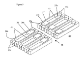
- Each mirror device 21 , 22 and 23 includes a pivoting member or platform 26 defined by first and second substantially-rectangular planar supporting regions 27 and 28 joined by a relatively-thin substantially-rectangular brace 29 extending therebetween.
- each planar surface is coated with a reflective coating, e.g. gold, for simultaneously reflecting a pair of sub-beams of light traveling along parallel paths, as will be hereinafter discussed.
- Each brace 29 acts like a lever and is pivotally mounted to anchor posts 30 and 31 via first and second torsional hinges 32 and 33 , respectively.
- the anchor posts 30 and 31 extend upwardly from the substrate 25 .
- the ends of the first torsional hinge 32 are connected to the anchor post 30 and the brace 29 along the axis ⁇ y .
- the ends of the second torsional hinge 32 are connected to the anchor post 31 and the brace 29 along the axis ⁇ y .
- each of the first and second torsional hinges 32 and 33 comprises a serpentine hinge, which are considerably more robust than conventional torsional beam hinges.
- the serpentine hinge is effectively longer than a normal torsional hinge, which spans the same distance, thereby providing greater deflection and strength, without requiring the space that would be needed to extend a normal full-length torsional hinge.
- each platform 26 is rotated by the selective activation of a first electrode 36 , which electro-statically attracts the first planar section 27 theretowards or by the selective activation of a second electrode 37 , which electro-statically attracts the second planar section 28 theretowards.
- a gap 38 is provided between the first and second electrodes 36 and 37 for receiving the anchor posts 31 , which extend from the substrate 25 to adjacent the platforms 26 .
- the angular position of the platforms 26 depend non-linearly on the voltage applied by the electrodes 36 (or 37 ), i.e. as the applied voltage is increased linearly, the incremental change in angular platform position is greater as the voltage increases. Accordingly, there is a maximum voltage, i.e. an angular platform position, at which the platform angular position becomes unstable and will uncontrollably tilt until hitting part of the lower structure, e.g. the electrode 36 . This maximum voltage sets the range of angular motion that the platform 26 can travel.
- the instability in the platform's angular position is a result of the distance between the platform 26 and the electrode 36 (the hot electrode) decreasing more rapidly at the outer free ends of the platform 26 than at the inner sections, nearer the pivot axis ⁇ y .
- the force per unit length along the platform 26 increases more rapidly at the outer free ends of the platform 26 than the inner sections.
- the field strength i.e. the force per unit area, that is sensed at the outer free ends of the platform 26 must be reduced. With reference to FIG. 5 , this is accomplished by providing the electrodes 36 and 37 with a two-step configuration.
- Upper steps 36 a and 37 a are positioned proximate the inner end of the platform 26 , i.e. the Y axis, while lower steps 36 b and 37 b are positioned under the outer free ends of the platform 26 , thereby making the gap between the platforms 26 and the electrodes 36 and 37 greater at the outer free end than the inner end.
- the area of the lower steps 36 b and 37 b can also be made smaller, thereby reducing the force per unit area sensed by the outer free end of the platform 26 .
- Multi-step electrodes e.g. three or more can also provide a more even distribution of force.
- electrode grounding shields 41 are positioned on the substrate 25 around or on either side of the first and second electrodes 36 and 37 forming electrode cavities, which are electrically isolated from each other.
- FIG. 5 illustrates C-shaped grounding shields 41 , which include lateral portions 41 a for partially surrounding the first and second electrodes 36 and 37 .
- the grounding shields 41 are kept at ground potential, i.e. the same as the mirrored platforms 26 , while one of the first and second electrodes is held at an activation voltage, e.g. 100 Volts.
- Trace lines 36 c and 37 c electrically connect the electrodes 36 and 37 , respectively, to a voltage supply (not shown). Since the trace lines 36 c and 37 c also act as a hot electrode, i.e. contributing to the total torque applied to the platform 26 , covering the traces 36 c and 37 c with a ground plane 43 ( FIG. 6 ) also reduces the force applied to the outer free end of the platform 26 .
- FIG. 6 also illustrates an alternative configuration for the electrode 36 , in which the two step hot electrode 36 is sunken slightly below a surrounding grounded metallic surface, which is a continuation of the ground plane 43 .
- a small vertical step 44 between the hot electrode 36 and the surrounding ground plane 43 is a dielectric surface that isolates the hot electrode 36 from the surrounding ground plane 43 .
- This arrangement reduces the angular drift of the platform 26 , which is caused by a build up of electrostatic charges on exposed dielectric or insulating surfaces. The electric field generated by these electrostatic charges perturbs the electric field generated by the applied voltage from the electrodes 36 and 37 , thereby causing the angular position of the platform 26 to drift over time.
- the present arrangement limits the exposed dielectric to the small vertical surface 44 , which generates electrostatic field lines that do not significantly affect the field lines between the hot electrodes 36 and 37 and the ground plane 43 .
- the vertical surface 44 can be under cut beneath the ground plane 43 at a slight negative angle ensuring that the gap between the hot electrode 36 and the ground plane 43 is substantially zero.
- the ground plane 43 could also be positioned slightly below the hot electrodes 36 and 37 to create the vertical step.
- the MEMs mirror devices 21 , 22 and 23 are for use in optical devices, i.e. wavelength blockers and multiple wavelength switches (see FIG. 23 ), which include a grating for dispersing the light into spectral wavelength component channels, it is an important performance requirement that the spectral response has a high rejection of light between the selected wavelength channels.
- optical devices i.e. wavelength blockers and multiple wavelength switches (see FIG. 23 )
- the spectral response has a high rejection of light between the selected wavelength channels.
- Unfortunately, in conventional MEMs devices light passes between the mirrors and is reflected off the substrate back into the optical device, thereby leading to a deterioration in the isolation between the wavelength channels.
- the present invention provides back reflection cusps 50 , defined by angled, curved or concave reflecting surfaces intersecting along a ridge, extending longitudinally below the gap between the platforms 26 , for scattering any light passing between the mirrored platforms 26 in a direction substantially parallel to the surface of the platforms 26 .
- additional platform shields 42 can be added to the underside of the planar supporting regions 27 and 28 , outside or inside of the electrode shields 41 .
- the two different sets of shields 41 and 42 do not overlap; however, as the platform 26 tilts the platform shields 42 begin to overlap the grounding shielding 41 .
- the added protection provided by overlapping shielding is particularly advantageous, when the tilt angle of the platform 26 is proportional to the voltage applied to the electrode 36 (or 37 ), such as in open loop configurations.
- a pair of internal gimbal ring MEMs mirror devices 131 and 132 are illustrated mounted adjacent each other on a substrate 133 .
- the present invention enables mirrors 134 and 135 to be positioned relatively close together, i.e. with a high fill factor, while still providing the two degrees of motion provided by the more complicated prior art.
- a first torsion hinge 137 preferably in the form of a rectangular beam, is fixed, proximate the middle thereof, to the substrate 133 via a central anchor post 138 .
- the supporting structure for the mirror device of the present invention is based on a single anchor post 138 , rather than the dual anchor points required in the aforementioned external gimbal ring devices.
- the first torsion hinge 137 provides for rotation ⁇ y about a first axis Y, and may also include a serpentine hinge 140 , as illustrated in mirror device 131 , or any other torsional hinge known in the art.
- Opposite sides of an internal gimbal ring 139 are connected to opposite ends of the first torsion hinge 137 , whereby the first torsion hinge 137 bisects the internal gimbal ring 139 .
- the internal gimbal ring 139 is preferably not flexible, but can take various geometric forms, although rectangular or circular frames would be the most convenient to fabricate and use.
- Spring arms 141 and 142 which define a second torsion hinge, extend outwardly from opposite sides of the internal gimbal ring 139 perpendicular to the first torsion hinge 137 .
- Each of the spring arms may also include a serpentine hinge as hereinbefore described.
- the second torsion hinge provides for rotation ⁇ x about a second axis X, which is perpendicular to the first axis Y, but still substantially in the same plane as the mirrors 134 and 135 .
- a generally rectangular platform 143 for supporting one of the mirrors 134 or 135 , is mounted on the ends of the spring arms 141 and 142 .
- the platform 143 is comprised of a pair of rectangular planar surfaces 144 and 145 joined together by a pair of elongated braces 147 and 148 , which extend on either side of the internal gimbal ring 139 parallel with the spring arms 141 and 142 .
- Fabrication of the preferred embodiment illustrated in FIGS. 8 and 9 is simplified by having all of the structural elements, i.e. the first torsional hinge 137 , the gimbal ring 139 , the spring arms 141 and 142 , and the first and second planar surfaces 144 and 145 , in the same upper substrate layer and having coplanar upper surfaces, whereby the same basic process steps are used as are used to fabricate the MEMs device illustrated in FIG. 1 .
- a single photolithographic step is used to identify the structural elements, followed by a deep reactive ion etching (DRIE) step used to remove the unwanted portions of the upper substrate.
- DRIE deep reactive ion etching
- the moveable elements in the upper substrate are released from the lower substrate by removal of a sacrificial layer therebetween.
- FIGS. 10 and 11 a illustrate an array of internal gimbal ring MEMs mirror devices 201 utilizing a first pair of serpentine torsional hinges 202 for pivoting a rectangular platform 203 , including first and second planar supporting regions 203 a and 203 b , about a first axis of rotation ⁇ x , and a second pair of serpentine torsional hinges 204 for rotating the platform 203 about a second axis of rotation ⁇ y above a base substrate 205 .
- the first and second planar supporting regions are joined by a pair of elongated braces 200 .
- the first pair of serpentine torsional hinges 202 extend from a single anchor post 206 , which extends upwardly from the base substrate 205 through the center of the platform 203 , i.e. at the intersection of the minor and major axes thereof. Outer ends of the first pair of torsional serpentine torsional hinges 202 are connected to a rectangular gimbal ring 208 , which surrounds the first pair of serpentine hinges 202 , at points along the minor axes ( ⁇ y ) of the platform 203 .
- the second pair of serpentine torsional hinges 204 extend from opposite sides of the gimbal ring 208 into contact with the platform 203 , at points along the major axis ( ⁇ x ) of the platform 203 .
- An alternative hinge structure for the mirror array 201 illustrated in FIG. 11 b , includes the first pair of serpentine torsional hinges 202 extending from anchor post 206 enabling the platform 203 to rotate about the y axis; however, only a single serpentine torsional hinge 204 is provided enabling rotation about the x axis. Accordingly, a C-shaped gimbal ring 209 extends from the ends of the hinges 202 , partially surrounding the hinges 202 , into contact with the end of the single hinge 204 .
- a set of four two-step electrodes 211 , 212 , 213 and 214 are provided (See FIG. 12 ); however, for the present invention only the first, second and third electrodes 211 , 212 and 213 are required to roll the mirrors out of alignment with any intermediate output ports and then back into alignment with a designated output port. As in FIG. 12 , only the first, second and third electrodes 211 , 212 and 213 are required to roll the mirrors out of alignment with any intermediate output ports and then back into alignment with a designated output port. As in FIG.
- each of the electrodes 211 , 212 , 213 and 214 include an upper step 211 a , 212 a , 213 a , and 214 a , and a lower step 211 b , 212 b , 213 b , 214 b , respectively, for reasons discussed hereinbefore. Accordingly, first, second and third voltages can be established between the platform 143 or 203 and the first electrode 211 , the second electrode 212 and the third electrode 213 , respectively. Initially, the first and second electrodes 211 and 212 are activated to rotate the platform 143 or 203 about ⁇ x .
- the first voltage is gradually lowered to zero, while the third voltage is gradually increased until it is equivalent to the second voltage (See FIG. 13 ).
- the first, second and third voltages are increased and decreased gradually, e.g. exponentially, as evidenced in FIG. 13 , which illustrates the voltages curves for the various electrodes (first, second and third) over the actuation time of the mirror device.
- Various mirror tilting patterns can be designed based on the desired characteristics, e.g. attenuation, of the light.
- FIGS. 14 and 15 An improved electrode configuration is illustrated in FIGS. 14 and 15 , in which a first two-step ⁇ y electrode 236 includes an upper U-shaped step 236 a , and a lower rectangular step 236 b .
- the arms of the U-shaped step 236 a extend from the lower step 236 b on opposite sides of the second hinge 204 beneath the first planar supporting region 203 a .
- a second two-step ⁇ y electrode 237 includes an upper U-shaped step 237 a , and a lower rectangular step 237 b .
- the arms of the U-shaped step 237 a extend from the lower rectangular step 237 b on opposite sides of the second hinge 204 beneath the second planar supporting region 203 b .
- a single two-step ⁇ x electrode 238 includes an upper U-shaped step 238 a , and lower rectangular steps 238 b extending from each arm of the upper U-shaped step.
- the single ⁇ x electrode 238 extends from adjacent the first ⁇ y electrode 236 to adjacent the second ⁇ y electrode 237 across the gap therebetween, and beneath one side of both the first and second planar supporting regions 203 a and 203 b .
- the lower steps 238 b provide a larger gap between the outer free ends of the platform 203 , when the platform is tilted towards the first or the second ⁇ y electrode 236 or 237 .
- the arms of the upper U-shaped step 238 b extend on opposite sides of the first pair of hinges 202 .
- the arms of the U-shaped step 238 a are three to five times wider than the arms of the U-shaped step 236 a or 237 a .
- Multi-step electrodes are also possible to further spread the application of force over the length of the platform 203 . Actuation of the electrodes is controlled by an electrode control 240 , as will be discussed hereinafter with reference to FIG. 19 .
- FIG. 16 illustrates the ideal case, in which the longitudinal axis of the first electrode 236 is aligned with the longitudinal axis X of the platform 203 .
- FIG. 17 illustrates the results of a mask misalignment during fabrication, in which the longitudinal axis X of the platform 203 has a + ⁇ x misalignment relative to the electrode axis.
- actuation of the first ⁇ y electrode 236 would introduce an undesirable tilt in the platform 203 towards the bottom left hand corner, which could not be compensated by the single ⁇ x electrode 238 .
- the illustrated mask misalignment in which the longitudinal axis X of the platform 203 has a ⁇ x misalignment relative to the electrode axis.
- actuation of the first ⁇ y electrode 236 would introduce an undesirable tilt in the platform 203 towards the top left hand corner.
- this tilt can be compensated for by applying a voltage to the single ⁇ x electrode 238 .
- the solution to the problem of mask misalignment is to introduce an intentional or predetermined ⁇ x misalignment, which would cancel or at least minimize any + ⁇ x misalignment and which could be compensated for by the single ⁇ x electrode 238 .
- FIG. 19 illustrates an electrode voltage vs time graph, detailing the voltages of the three electrodes 236 , 237 and 238 as the platform 203 is switched from one position to another by an electrode control, i.e. from reflecting light from one port to another, without traveling directly, i.e. without reflecting light into any intermediate ports.
- the voltage VyR of the first ⁇ y electrode 236 is gradually decreased as the voltage Vx of the single ⁇ x electrode 238 is increased.
- the voltage VyL of the second ⁇ y electrode 237 gradually increases.
- the voltage Vx is decreased to a minimum amount, assuming no compensation voltages are required.
- the electrodes 236 , 237 and 238 must also be constructed correspondingly smaller.
- the electrodes due to the fact that the electrodes necessarily become thinner, while sharing the same mirror section, stable tilt angles are difficult to achieve at high resonant frequencies. Accordingly, the size requirement of the electrode, and the required electrode spacing become the limiting factor in determining the maximum fill factor.
- FIGS. 20 and 21 An alternative embodiment of a three electrode configuration is illustrated in FIGS. 20 and 21 , in which two parallel arrays of platforms 253 and 254 are made smaller than the original platforms 203 with first and second two-step ⁇ y electrodes 256 and 257 positioned therebelow.
- a single ⁇ x electrode 258 is positioned below each offset section 259 and 260 , which extend from the side of the platforms 253 and 254 , respectively, adjacent the mid-section thereof, i.e. the area of first and second hinges 251 and 252 .
- This arrangement enables the single ⁇ x electrode 258 to be separated from the other two electrodes 256 and 257 , and therefore, be larger in size, which enables the electrostatic torque to be increased for a common voltage.
- the added separation between the electrodes 256 , 257 and 258 minimizes the angular instabilities, when the single ⁇ x electrode 238 is actuated, and reduces the amount of electrical x-talk.
- the two-step ⁇ x electrodes 256 and 257 include the ground plane arrangement as disclosed in FIG. 6 with hot electrodes sunken relative to a surrounding ground plane, and only a vertically extending dielectric layer, which provides a substantially zero-width vertical gap between the hot electrode and the ground plane.
- a first planar section 253 a of one platform 253 from the first array is positioned beside a second planar section 254 b of an adjacent platform 254 from the second array, as in FIGS. 20 and 21 , whereby adjacent mirrors have offset x axes X 1 and X 2 , and every other platform pivots about the same laterally extending x axis.
- Each or the platforms 253 and 254 are also rotatable about separate parallel longitudinal axes. Only the relatively closely disposed planar sections would require reflective material thereon, and reflective cusps 260 would only be required therebelow ( FIG. 22 ).
- Substrate-mounted, grounded cross-talk shields 261 and platform mounted cross-talk shields 262 are provided to further minimize the amount of electrical cross-talk between adjacent mirrors.
- the platform mount cross-talk shields 262 are preferably mounted outside of the platform mounted cross-talk shields 262 with enough spacing to enable rotation about both the x and the y axis; however, any combination for offsetting the shields 261 and 262 is possible.
- FIGS. 23 to 25 illustrate another embodiment of the reflective cusps specific to the interlaced mirrors of FIGS. 20 to 22 .
- a portion of the reflective cusp 260 a is positioned below the platforms 253 extending from an inner end proximate the anchor post to proximate the midway point of the first planar section 253 a
- a portion of the reflective cusp 260 b is positioned below the platforms 254 extending from proximate the anchor post to proximate the midway point of the second planar section 254 b .
- the portions of the reflective cusp 260 a and 260 b can extend any suitable length, whereby the ends thereof are directly adjacent each other providing overlapping protection.
- the portions of the reflective cusps 260 a and 260 b can have the same or different lengths.
- FIGS. 26 and 27 A simple alternative to the interlaced mirrors of FIGS. 20 to 25 are illustrated in FIGS. 26 and 27 , in which a first array of 1-d Piano MEMs mirrors 273 pivot about a first lateral axis X 1 via a single pair of torsional hinges 274 , and a second array of 1-d Piano MEMs mirrors 275 pivot about a second lateral axis X 2 via a single pair of torsional hinges 276 .
- a first sections 273 a and 275 a of the platforms 273 and 275 are preferably larger than a second sections 273 b and 275 b , respectively, to enable the size of single electrodes 277 and 278 to be wider and/or shorter than the size of the second sections 273 b and 275 b .
- Activation of the single electrodes 277 and 278 attracts the first sections 273 a and 275 a , respectively, thereby pivoting the platforms 273 and 275 about the first lateral axes X 1 and X 2 , respectively.
- the platforms 273 and 275 returns to the horizontal set position when the single electrodes 277 and 278 are deactivated due to the resilient spring force inherent in the platforms 273 and 275 .
- the second sections 273 b and 275 b form an array of closely packed reflective surfaces between the first and second lateral axes X 1 and X 2 .
- the electrodes 277 and 278 are two step electrodes, as above, and include the ground plane arrangement as disclosed in FIG. 6 with hot electrodes sunken relative to a surrounding ground plane, and only a vertically extending dielectric layer, which provides a substantially zero-width vertical gap between the hot electrode and the ground plane.
- the mirror to mirror electrical crosstalk can be reduced even for relatively small mirror pitches, e.g. ⁇ 70 um, because the closest adjacent electrodes are separated by a mirror length in one direction, and by up to half a mirror pitch in the other direction.
- the voltage-tilt angle and the resonant frequency characteristics are also improved for low pitches due to the increase electrode area and resultant electrostatic torque.
- the electrical pin-out is reduced to one connection per mirror.
- the “piano” MEMs mirror devices according to the present invention are particularly useful in a wavelength switch 301 illustrated in FIGS. 28 , 29 and 30 .
- a beam of light with a plurality of different wavelength channels is launched via an input/output assembly 302 , which comprises a plurality of input/output ports, e.g. first, second, third and fourth input/output ports 303 , 304 , 305 and 306 , respectively.
- the beam is directed to an element having optical power, such as concave mirror 309 , which redirects the beam to a dispersive element 311 , e.g. a Bragg grating.
- the dispersive element separates the beam into the distinct wavelength channels ( ⁇ 1 , ⁇ 2 , ⁇ 3 ), which are again directed to an element having optical power, e.g. the concave mirror 309 .
- the concave mirror 309 redirects the various wavelength channels to an array of “piano” MEMs mirror devices 312 according to the present invention, which are independently controlled to direct the various wavelength channels back to whichever input/output port is desired. Wavelength channels designated for the same port are reflected back off the concave mirror 309 to the dispersive element 311 for recombination and redirection off the concave mirror 309 to the desired input/output port.
- the concave mirror 309 can b e replaced by a single lens with other elements of the switch on either side thereof or by a pair of lenses with the dispersive element 311 therebetween.
- the input/output assembly 302 includes a plurality of input/output fibers 313 a to 313 d with a corresponding collimating lens 314 a to 314 d .
- a single lens 316 is used to convert a spatial offset between the input/output ports into an angular offset.
- FIG. 30 illustrates a preferred embodiment of the input/output assembly, in which the unwanted effects of polarization diversity are eliminated by the use of a birefringent crystal 317 and a waveplate 318 .
- the lens 316 directs each beam through the birefringent crystal 317 , which separates the beam into two orthogonally polarized sub-beams (o and e).
- the half waveplate 318 is positioned in the path of one of the sub-beams for rotating the polarization thereof by 90°, so that both of the sub-beams have the same polarization for transmission into the remainder of the switch.
- the waveplate 318 is a quarter waveplate and rotates one of the sub-beams by 45° in one direction, while another quarter waveplate 319 rotates the other sub-beam by 45° in the opposite direction, whereby both sub-beams have the same polarization.
- the polarization of one (or both) of the similarly polarized sub-beams are rotated by the waveplate(s) 318 (and 319 ), so that the sub-beams become orthogonally polarized.
- the orthogonally polarized sub-beams are then recombined by the birefringent crystal 317 and output the appropriate input/output port.
- the micro-electro-mechanical devices according to the present invention are particularly well suited for use in switching devices with polarization diversity front ends, since they provide a pair of reflecting surfaces, i.e. one for each sub-beam
Abstract
Description
Claims (15)
Priority Applications (1)
| Application Number | Priority Date | Filing Date | Title |
|---|---|---|---|
| US11/075,650 US7167613B2 (en) | 2002-05-28 | 2005-03-10 | Interlaced array of piano MEMs micromirrors |
Applications Claiming Priority (7)
| Application Number | Priority Date | Filing Date | Title |
|---|---|---|---|
| US38310602P | 2002-05-28 | 2002-05-28 | |
| US10/445,360 US6934439B2 (en) | 2002-05-28 | 2003-05-27 | Piano MEMs micromirror |
| US50421003P | 2003-09-22 | 2003-09-22 | |
| US53701204P | 2004-01-20 | 2004-01-20 | |
| US55856304P | 2004-04-02 | 2004-04-02 | |
| US10/850,407 US6968101B2 (en) | 2002-05-28 | 2004-05-21 | Electrode configuration for piano MEMs micromirror |
| US11/075,650 US7167613B2 (en) | 2002-05-28 | 2005-03-10 | Interlaced array of piano MEMs micromirrors |
Related Parent Applications (1)
| Application Number | Title | Priority Date | Filing Date |
|---|---|---|---|
| US10/850,407 Continuation-In-Part US6968101B2 (en) | 2002-05-28 | 2004-05-21 | Electrode configuration for piano MEMs micromirror |
Publications (2)
| Publication Number | Publication Date |
|---|---|
| US20050180685A1 US20050180685A1 (en) | 2005-08-18 |
| US7167613B2 true US7167613B2 (en) | 2007-01-23 |
Family
ID=46304109
Family Applications (1)
| Application Number | Title | Priority Date | Filing Date |
|---|---|---|---|
| US11/075,650 Expired - Lifetime US7167613B2 (en) | 2002-05-28 | 2005-03-10 | Interlaced array of piano MEMs micromirrors |
Country Status (1)
| Country | Link |
|---|---|
| US (1) | US7167613B2 (en) |
Cited By (5)
| Publication number | Priority date | Publication date | Assignee | Title |
|---|---|---|---|---|
| EP1927873A1 (en) | 2006-11-30 | 2008-06-04 | JDS Uniphase Corporation | Micromirror device with a hybrid parallel plate and comb drive actuator |
| EP2006247A2 (en) | 2007-06-21 | 2008-12-24 | JDS Uniphase Corporation | MEMS device with an angular vertical comb actuator |
| US20090190202A1 (en) * | 2008-01-29 | 2009-07-30 | Moidu Abdul Jaleel K | Mems micromirror devices with anti-reflective structures |
| US20090268270A1 (en) * | 2008-04-29 | 2009-10-29 | Micralyne Inc. | Mems device with independent rotation in two axes of rotation |
| US8654434B2 (en) * | 2010-07-20 | 2014-02-18 | Oclaro (New Jersey), Inc. | WSS with pixel gap compensation |
Citations (11)
| Publication number | Priority date | Publication date | Assignee | Title |
|---|---|---|---|---|
| US5315429A (en) * | 1993-01-04 | 1994-05-24 | Xerox Corporation | Micromechanical light modulator with optically interlaced output |
| US6327855B1 (en) | 2000-02-04 | 2001-12-11 | Jds Uniphase Inc. | Actuators including serpentine arrangements of alternating actuating and opposing segments and related methods |
| US20020126455A1 (en) | 2001-02-14 | 2002-09-12 | Wood Robert L. | Tiled microelectromechanical device modules and fabrication methods |
| US6454421B2 (en) | 1999-07-13 | 2002-09-24 | Input/Output, Inc. | Dual axis micro machined mirror device |
| US6491404B2 (en) | 2001-02-23 | 2002-12-10 | Jds Uniphase Corporation | Microelectromechanical apparatus with tiltable bodies including variable tilt-stop engaging portions and methods of operation and fabrication therefor |
| US6529652B1 (en) | 2001-03-15 | 2003-03-04 | Tellium, Inc. | Optical switch and method for aligning optical switch components |
| US6533947B2 (en) | 2001-02-07 | 2003-03-18 | Transparent Optical, Inc. | Microelectromechanical mirror and mirror array |
| US6535319B2 (en) | 2001-07-03 | 2003-03-18 | Network Photonics, Inc. | Free-space optical wavelength routing element based on stepwise controlled tilting mirrors |
| US20030052569A1 (en) | 2001-09-18 | 2003-03-20 | Dhuler Vijayakumar Rudrappa | Electrostatic actuators in micro-electromechanical systems |
| US6778728B2 (en) * | 2001-08-10 | 2004-08-17 | Corning Intellisense Corporation | Micro-electro-mechanical mirror devices having a high linear mirror fill factor |
| US6992810B2 (en) * | 2002-06-19 | 2006-01-31 | Miradia Inc. | High fill ratio reflective spatial light modulator with hidden hinge |
-
2005
- 2005-03-10 US US11/075,650 patent/US7167613B2/en not_active Expired - Lifetime
Patent Citations (11)
| Publication number | Priority date | Publication date | Assignee | Title |
|---|---|---|---|---|
| US5315429A (en) * | 1993-01-04 | 1994-05-24 | Xerox Corporation | Micromechanical light modulator with optically interlaced output |
| US6454421B2 (en) | 1999-07-13 | 2002-09-24 | Input/Output, Inc. | Dual axis micro machined mirror device |
| US6327855B1 (en) | 2000-02-04 | 2001-12-11 | Jds Uniphase Inc. | Actuators including serpentine arrangements of alternating actuating and opposing segments and related methods |
| US6533947B2 (en) | 2001-02-07 | 2003-03-18 | Transparent Optical, Inc. | Microelectromechanical mirror and mirror array |
| US20020126455A1 (en) | 2001-02-14 | 2002-09-12 | Wood Robert L. | Tiled microelectromechanical device modules and fabrication methods |
| US6491404B2 (en) | 2001-02-23 | 2002-12-10 | Jds Uniphase Corporation | Microelectromechanical apparatus with tiltable bodies including variable tilt-stop engaging portions and methods of operation and fabrication therefor |
| US6529652B1 (en) | 2001-03-15 | 2003-03-04 | Tellium, Inc. | Optical switch and method for aligning optical switch components |
| US6535319B2 (en) | 2001-07-03 | 2003-03-18 | Network Photonics, Inc. | Free-space optical wavelength routing element based on stepwise controlled tilting mirrors |
| US6778728B2 (en) * | 2001-08-10 | 2004-08-17 | Corning Intellisense Corporation | Micro-electro-mechanical mirror devices having a high linear mirror fill factor |
| US20030052569A1 (en) | 2001-09-18 | 2003-03-20 | Dhuler Vijayakumar Rudrappa | Electrostatic actuators in micro-electromechanical systems |
| US6992810B2 (en) * | 2002-06-19 | 2006-01-31 | Miradia Inc. | High fill ratio reflective spatial light modulator with hidden hinge |
Cited By (14)
| Publication number | Priority date | Publication date | Assignee | Title |
|---|---|---|---|---|
| EP1927873A1 (en) | 2006-11-30 | 2008-06-04 | JDS Uniphase Corporation | Micromirror device with a hybrid parallel plate and comb drive actuator |
| US20080137165A1 (en) * | 2006-11-30 | 2008-06-12 | Moidu Abduljaleel K | Micromirror device with a hybrid actuator |
| US7715076B2 (en) | 2006-11-30 | 2010-05-11 | Jds Uniphase Corporation | Micromirror device with a hybrid actuator |
| US20080316577A1 (en) * | 2007-06-21 | 2008-12-25 | Moidu Abdul Jaleel K | Mems device with an angular vertical comb actuator |
| EP2006247A2 (en) | 2007-06-21 | 2008-12-24 | JDS Uniphase Corporation | MEMS device with an angular vertical comb actuator |
| US7817331B2 (en) | 2007-06-21 | 2010-10-19 | Jds Uniphase Corporation | MEMS device with an angular vertical comb actuator |
| US20090190202A1 (en) * | 2008-01-29 | 2009-07-30 | Moidu Abdul Jaleel K | Mems micromirror devices with anti-reflective structures |
| US7903318B2 (en) | 2008-01-29 | 2011-03-08 | Jds Uniphase Corporation | MEMS micromirror devices with anti-reflective structures |
| US20090268270A1 (en) * | 2008-04-29 | 2009-10-29 | Micralyne Inc. | Mems device with independent rotation in two axes of rotation |
| US20100265555A1 (en) * | 2008-04-29 | 2010-10-21 | Micralyne Inc. | Mems device with independent rotation in two axes of rotation |
| US8208192B2 (en) | 2008-04-29 | 2012-06-26 | Micralyne Inc. | MEMS device with independent rotation in two axes of rotation |
| US8368983B2 (en) | 2008-04-29 | 2013-02-05 | Micralyne, Inc. | MEMS device with independent rotation in two axes of rotation |
| US9036229B2 (en) | 2008-04-29 | 2015-05-19 | Micralyne Inc. | MEMS device with independent rotation in two axes of rotation |
| US8654434B2 (en) * | 2010-07-20 | 2014-02-18 | Oclaro (New Jersey), Inc. | WSS with pixel gap compensation |
Also Published As
| Publication number | Publication date |
|---|---|
| US20050180685A1 (en) | 2005-08-18 |
Similar Documents
| Publication | Publication Date | Title |
|---|---|---|
| US7010188B2 (en) | Electrode configuration for piano MEMs micromirror | |
| US7302132B2 (en) | Electrical x-talk shield for MEMs micromirrors | |
| US6934439B2 (en) | Piano MEMs micromirror | |
| US7203413B2 (en) | Sunken electrode configuration for MEMs micromirror | |
| US7616372B2 (en) | Piano MEMS with hidden hinge | |
| US7095546B2 (en) | Micro-electro-mechanical-system two dimensional mirror with articulated suspension structures for high fill factor arrays | |
| US6909530B2 (en) | Movable microstructure with contactless stops | |
| US6212309B1 (en) | Optical cross point switch using deformable micromirror | |
| US7167613B2 (en) | Interlaced array of piano MEMs micromirrors | |
| CA2764403A1 (en) | Micromirror element and micromirror array | |
| US7110637B2 (en) | Two-step electrode for MEMs micromirrors | |
| JP2992887B2 (en) | Optical intersection switch using deformable micro mirror | |
| EP1479647B1 (en) | Electrical cross-talk shield for MEMs micromirrors | |
| EP1479646B1 (en) | Electrode configuration for pivotable MEMS micromirror | |
| CA2482165C (en) | Sunken electrode configuration for mems micromirror | |
| CA2468132C (en) | Electrode configuration for piano mems micromirror | |
| CA2501012C (en) | Interlaced array of piano mems micromirrors | |
| US6757093B2 (en) | MEMS reflectors having tail portions that extend inside a recess and head portions that extend outside the recess and methods of forming same | |
| CA2468139C (en) | Electrical cross-talk shields for mems micromirrors |
Legal Events
| Date | Code | Title | Description |
|---|---|---|---|
| AS | Assignment |
Owner name: JDS UNIPHASE INC., CANADA Free format text: ASSIGNMENT OF ASSIGNORS INTEREST;ASSIGNORS:MILLER, JOHN M.;JIN, WENLIN;KEYWORTH, BARRIE;AND OTHERS;REEL/FRAME:016381/0874 Effective date: 20050223 |
|
| STCF | Information on status: patent grant |
Free format text: PATENTED CASE |
|
| FPAY | Fee payment |
Year of fee payment: 4 |
|
| FPAY | Fee payment |
Year of fee payment: 8 |
|
| AS | Assignment |
Owner name: JDS UNIPHASE CORPORATION, CALIFORNIA Free format text: ASSIGNMENT OF ASSIGNORS INTEREST;ASSIGNOR:JDS UNIPHASE INC.;REEL/FRAME:036087/0320 Effective date: 20150626 |
|
| AS | Assignment |
Owner name: LUMENTUM OPERATIONS LLC, CALIFORNIA Free format text: ASSIGNMENT OF ASSIGNORS INTEREST;ASSIGNOR:JDS UNIPHASE CORPORATION;REEL/FRAME:036420/0340 Effective date: 20150731 |
|
| FEPP | Fee payment procedure |
Free format text: PAYOR NUMBER ASSIGNED (ORIGINAL EVENT CODE: ASPN); ENTITY STATUS OF PATENT OWNER: LARGE ENTITY |
|
| AS | Assignment |
Owner name: LUMENTUM OPERATIONS LLC, CALIFORNIA Free format text: CORRECTIVE ASSIGNMENT TO CORRECT THE PATENTS LISTED ON PAGE A-A33 PREVIOUSLY RECORDED ON REEL 036420 FRAME 0340. ASSIGNOR(S) HEREBY CONFIRMS THE PATENT NUMBERS 7,868,247 AND 6,476,312 WERE LISTED IN ERROR AND SHOULD BE REMOVED;ASSIGNOR:JDS UNIPHASE CORPORATION;REEL/FRAME:037562/0513 Effective date: 20150731 Owner name: LUMENTUM OPERATIONS LLC, CALIFORNIA Free format text: CORRECTIVE ASSIGNMENT TO CORRECT INCORRECT PATENTS 7,868,247 AND 6,476,312 ON PAGE A-A33 PREVIOUSLY RECORDED ON REEL 036420 FRAME 0340. ASSIGNOR(S) HEREBY CONFIRMS THE ASSIGNMENT;ASSIGNOR:JDS UNIPHASE CORPORATION;REEL/FRAME:037562/0513 Effective date: 20150731 |
|
| AS | Assignment |
Owner name: LUMENTUM OPERATIONS LLC, CALIFORNIA Free format text: CORRECTIVE ASSIGNMENT TO CORRECT THE PATENTS LISTED ON PAGE A-A33 PATENT NUMBERS 7,868,247 AND 6,476,312 WERE LISTED IN ERROR AND SHOULD BE REMOVED. PREVIOUSLY RECORDED ON REEL 036420 FRAME 0340. ASSIGNOR(S) HEREBY CONFIRMS THE ASSIGNMENT;ASSIGNOR:JDS UNIPHASE CORPORATION;REEL/FRAME:037627/0641 Effective date: 20150731 Owner name: LUMENTUM OPERATIONS LLC, CALIFORNIA Free format text: CORRECTIVE ASSIGNMENT TO CORRECT PATENTS 7,868,247 AND 6,476,312 LISTED ON PAGE A-A33 PREVIOUSLY RECORDED ON REEL 036420 FRAME 0340. ASSIGNOR(S) HEREBY CONFIRMS THE ASSIGNMENT;ASSIGNOR:JDS UNIPHASE CORPORATION;REEL/FRAME:037627/0641 Effective date: 20150731 |
|
| FEPP | Fee payment procedure |
Free format text: PAYOR NUMBER ASSIGNED (ORIGINAL EVENT CODE: ASPN); ENTITY STATUS OF PATENT OWNER: LARGE ENTITY Free format text: PAYER NUMBER DE-ASSIGNED (ORIGINAL EVENT CODE: RMPN); ENTITY STATUS OF PATENT OWNER: LARGE ENTITY |
|
| MAFP | Maintenance fee payment |
Free format text: PAYMENT OF MAINTENANCE FEE, 12TH YEAR, LARGE ENTITY (ORIGINAL EVENT CODE: M1553) Year of fee payment: 12 |
|
| AS | Assignment |
Owner name: DEUTSCHE BANK AG NEW YORK BRANCH, AS COLLATERAL AGENT, NEW YORK Free format text: PATENT SECURITY AGREEMENT;ASSIGNORS:LUMENTUM OPERATIONS LLC;OCLARO FIBER OPTICS, INC.;OCLARO, INC.;REEL/FRAME:047788/0511 Effective date: 20181210 Owner name: DEUTSCHE BANK AG NEW YORK BRANCH, AS COLLATERAL AG Free format text: PATENT SECURITY AGREEMENT;ASSIGNORS:LUMENTUM OPERATIONS LLC;OCLARO FIBER OPTICS, INC.;OCLARO, INC.;REEL/FRAME:047788/0511 Effective date: 20181210 |
|
| AS | Assignment |
Owner name: LUMENTUM OPERATIONS LLC, CALIFORNIA Free format text: RELEASE BY SECURED PARTY;ASSIGNOR:DEUTSCHE AG NEW YORK BRANCH;REEL/FRAME:051287/0556 Effective date: 20191212 Owner name: OCLARO FIBER OPTICS, INC., CALIFORNIA Free format text: RELEASE BY SECURED PARTY;ASSIGNOR:DEUTSCHE AG NEW YORK BRANCH;REEL/FRAME:051287/0556 Effective date: 20191212 Owner name: OCLARO, INC., CALIFORNIA Free format text: RELEASE BY SECURED PARTY;ASSIGNOR:DEUTSCHE AG NEW YORK BRANCH;REEL/FRAME:051287/0556 Effective date: 20191212 |