US7190861B2 - Monolithic semiconductor light source with spectral controllability - Google Patents
Monolithic semiconductor light source with spectral controllability Download PDFInfo
- Publication number
- US7190861B2 US7190861B2 US10/758,343 US75834304A US7190861B2 US 7190861 B2 US7190861 B2 US 7190861B2 US 75834304 A US75834304 A US 75834304A US 7190861 B2 US7190861 B2 US 7190861B2
- Authority
- US
- United States
- Prior art keywords
- ase
- wavelength
- seed
- optical
- light source
- Prior art date
- Legal status (The legal status is an assumption and is not a legal conclusion. Google has not performed a legal analysis and makes no representation as to the accuracy of the status listed.)
- Expired - Fee Related, expires
Links
Images


Classifications
-
- H—ELECTRICITY
- H04—ELECTRIC COMMUNICATION TECHNIQUE
- H04B—TRANSMISSION
- H04B10/00—Transmission systems employing electromagnetic waves other than radio-waves, e.g. infrared, visible or ultraviolet light, or employing corpuscular radiation, e.g. quantum communication
- H04B10/29—Repeaters
- H04B10/291—Repeaters in which processing or amplification is carried out without conversion of the main signal from optical form
- H04B10/2912—Repeaters in which processing or amplification is carried out without conversion of the main signal from optical form characterised by the medium used for amplification or processing
- H04B10/2916—Repeaters in which processing or amplification is carried out without conversion of the main signal from optical form characterised by the medium used for amplification or processing using Raman or Brillouin amplifiers
-
- G—PHYSICS
- G02—OPTICS
- G02B—OPTICAL ELEMENTS, SYSTEMS OR APPARATUS
- G02B6/00—Light guides; Structural details of arrangements comprising light guides and other optical elements, e.g. couplings
- G02B6/10—Light guides; Structural details of arrangements comprising light guides and other optical elements, e.g. couplings of the optical waveguide type
- G02B6/12—Light guides; Structural details of arrangements comprising light guides and other optical elements, e.g. couplings of the optical waveguide type of the integrated circuit kind
-
- G—PHYSICS
- G02—OPTICS
- G02B—OPTICAL ELEMENTS, SYSTEMS OR APPARATUS
- G02B6/00—Light guides; Structural details of arrangements comprising light guides and other optical elements, e.g. couplings
- G02B6/24—Coupling light guides
- G02B6/42—Coupling light guides with opto-electronic elements
- G02B6/4201—Packages, e.g. shape, construction, internal or external details
- G02B6/4204—Packages, e.g. shape, construction, internal or external details the coupling comprising intermediate optical elements, e.g. lenses, holograms
- G02B6/4213—Packages, e.g. shape, construction, internal or external details the coupling comprising intermediate optical elements, e.g. lenses, holograms the intermediate optical elements being polarisation selective optical elements
-
- G—PHYSICS
- G02—OPTICS
- G02B—OPTICAL ELEMENTS, SYSTEMS OR APPARATUS
- G02B6/00—Light guides; Structural details of arrangements comprising light guides and other optical elements, e.g. couplings
- G02B6/24—Coupling light guides
- G02B6/42—Coupling light guides with opto-electronic elements
- G02B6/4201—Packages, e.g. shape, construction, internal or external details
- G02B6/4204—Packages, e.g. shape, construction, internal or external details the coupling comprising intermediate optical elements, e.g. lenses, holograms
- G02B6/4215—Packages, e.g. shape, construction, internal or external details the coupling comprising intermediate optical elements, e.g. lenses, holograms the intermediate optical elements being wavelength selective optical elements, e.g. variable wavelength optical modules or wavelength lockers
Definitions
- This invention relates to optical systems in general, and more particularly to systems for amplifying optical signals.
- Dense wavelength-division multiplexing is currently the preferred method for satisfying bandwidth demand for fiber-optic long-haul transport in telecommunication systems.
- DWDM Dense wavelength-division multiplexing
- fiber nonlinearities, fiber loss, and amplified spontaneous emission (ASE) all act to degrade the signal-to-noise ratio of the data signal.
- ASE amplified spontaneous emission
- the optical signal needs to be periodically amplified and eventually electrically regenerated so as to maintain the signal integrity.
- a typical 40 channel DWDM system using Erbium-doped fiber amplifiers (EDFA's) generally has an amplifier span spacing of about 80 km and OEO regeneration distances of around 500–600 km.
- OEO regeneration is responsible for a much larger percentage of overall system cost than amplifiers. It is, therefore, desirable to extend the regeneration distance wherever possible.
- Raman fiber amplifier technologies have emerged as a highly promising building block to allow DWDM transmission for distances greater than 1500 km without OEO regeneration. This is particularly important inasmuch as the majority of data traffic on a telecommunications network typically has a destination distance which exceeds 1000 km.
- Raman fiber amplifiers generally use the transmission fiber itself as the gain medium. Thus, the signal passing through the fiber is amplified as it propagates. Because of their distributed nature, Raman amplifiers present several significant advantages over EDFA technologies:
- the Raman gain profile of optical fiber is much broader and smoother than that of EDFA's.
- the combination of several pump laser wavelengths can provide overall gain profiles as broad as near 100 nm with less than 1 dB gain ripple, thus reducing the gain ripple and tilting effects generally associated with EDFA's.
- Inline EDFA's typically operate in saturation mode where the gains of the amplifier for individual wavelength channels are a function of total input signal power.
- the gains for all of the other channels change, causing network transients, distortions and misbalances.
- Raman amplifiers typically work in a linear mode where the gain of each channel is independent of all of the other channels.
- Raman-assisted transmission generally compares favorably to EDFA-only systems, leading to better system quality factors, longer amplifier spans, and hence longer DWDM transmission before the need for OEO regeneration.
- HFC-CATV hybrid fiber coaxial cable (community antenna) TV
- SCM subcarrier multiplexing
- QAM multilevel quadrature amplitude modulation
- EDFA's up to 25 dBm
- limiting span spacing typically 30–40 km
- Raman amplification in fiber are based on the process of stimulated Raman scattering (SRS).
- SRS stimulated Raman scattering
- the Raman gain profile of standard fused silica fiber is very broad due to the amorphous nature of the glass.
- the Raman gain increases nearly linearly from the pump frequency towards a maximum at about 13.2 THz (100 nm) and then falls off fairly sharply.
- the Raman gain profile will have a maximum near 1550 nm, with a usable gain bandwidth of ⁇ 30 nm (see FIG. 1 ).
- the magnitude of the Raman gain in optical fiber depends on the respective compositional doping elements.
- the normalized gain spectral shape is much less sensitive to glass composition for most fibers typically used.
- the Raman gain increases nearly linearly, in dB, with increasing pump power. Nearly 10 dB of Raman gain is typical for 500 mW of pump power injected into 40 km of Corning SMF-28TM fiber.
- the upper limit of realistically useful Raman gain is generally limited by the double Rayleigh scattering process. At that upper limit, the Rayleigh back scattering causes multiple reflections of both the ASE and the signal, thus causing performance degradation of the transmission. Double Rayleigh scattering becomes prominent as the Raman gain reaches above 15 dB.
- the Raman gain spectrum can be tailored in shape and width by selecting the appropriate pump laser wavelength spectrum.
- To construct a 100 nm bandwidth Raman amplifier up to 8 pump wavelengths, ranging from 1430 nm to 1520 nm, are needed for the amplification of signals in the 1530 nm to 1620 nm band with less than 1 dB gain ripple.
- the 1 dB gain ripple is due in part to the fine and sharp structures near the peak of the gain profile shown in FIG. 1 .
- Raman amplifiers One significant characteristic of Raman amplifiers is that Raman amplification is effective only if the signal beam has the same polarization as that of the pump.
- two diode lasers, with orthogonal polarization are generally used for each pump wavelength.
- another approach to solve this issue is to use various polarization scrambling techniques.
- current polarization scrambling techniques are generally relatively costly and bulky, and have unproven reliability.
- Raman scattering due to its fast response time, causes amplitude noise in the pump lasers to be proportionally transferred to the gain fluctuations.
- FIG. 2 when a noise-free signal beam propagates along the Raman amplified transmission fiber, the signal data set experiences a time-dependent amplification. As a result of this phenomena, the output signal beam carries amplitude noise.
- the noise transfer from pump laser to the signal beam depends on the pump geometry employed.
- the signal beam experiences the gain through its entire traveling time in the fiber, and the RIN of the pump laser is then effectively averaged over the travel time.
- the signal beam traveling time is about 100 microseconds.
- the high frequency RIN components typically above 1 MHz, are substantially insensitive to the signal transmission quality ( FIG. 3 ). This suppression of the RIN transfer from pump to signal is one of the main reasons that “backward pumping” remains the most popular scheme for Raman amplification in telecommunication systems.
- the average of the pump RIN is determined only by the walk-off time between the signal and pump generated by dispersion of the fiber.
- the RIN transfer from pump to signal remains effective for much higher frequency components, as shown in FIG. 3 .
- the RIN of the pump lasers must then generally be limited to ⁇ 150 dB/Hz. This requirement is often difficult to achieve for the commonly-used frequency-stabilized Fabry-Perot lasers.
- distributed feedback (DFB) lasers have generally been used for forward pumping applications.
- the present invention provides solutions to a number of the challenges described above.
- a system for amplifying optical signals comprising: an optical fiber for carrying the optical signals; a high power broadband light source; and a connector for introducing the high power broadband light source into the optical fiber as a Raman pump so as to induce Raman amplification of the optical signals within the fiber.
- a method for amplifying optical signals comprising: introducing a high power broadband light source into an optical fiber carrying the optical signals so that the high power broadband light source acts as a Raman pump so as to induce Raman amplification of the optical signals within the fiber.
- a spectrally filtered high power broadband light source comprising a spectrally filtered amplified spontaneous emission (ASE) generated from an optical component.
- ASE amplified spontaneous emission
- FIG. 1 is a schematic diagram showing the normalized Raman gain spectrum of standard single mode fiber, at a pump wavelength of 1450 nm;
- FIG. 2 is a schematic diagram showing distributed Raman amplification using forward pumping
- FIG. 3 is a schematic diagram showing the RIN transfer spectrum for a co-pumped and counter-pumped Raman amplifier with 10 dB of gain;
- FIG. 4 is a schematic diagram showing the power evolution of pump diode lasers along the fiber path
- FIG. 5 is a schematic diagram showing the simulated Raman gain shape achieved using (i) six discrete pump wavelengths, and (ii) two broadband light sources;
- FIG. 6 is a schematic diagram showing depolarizers for long and short coherence light sources
- FIG. 7 is a schematic diagram showing the reduction of FWM achieved in a Raman amplifier pump using (i) discrete pump wavelengths, and (ii) a broadband ASE source;
- FIG. 8 is a schematic diagram showing a broadband ASE Raman pump source
- FIG. 9 is a schematic diagram illustrating how multiple ASE sources can be superimposed so as to form a composite ASE spectrum for Raman pumping
- FIG. 10 is a schematic diagram illustrating a first preferred embodiment for forming a broadband ASE source
- FIG. 11 is a schematic diagram illustrating a second preferred embodiment for forming a broadband ASE source
- FIG. 12 is a schematic diagram illustrating a third preferred embodiment for forming a broadband ASE source
- FIG. 13 is a schematic diagram illustrating a fourth preferred embodiment for forming a broadband ASE source
- FIG. 14 is a diagram showing the use of a discrete seed and booster to generate high power ASE
- FIG. 15 is a schematic diagram illustrating a fifth preferred embodiment for forming a broadband ASE source
- FIG. 16 is a schematic illustration showing a booster power module (BPM) simulated transverse mode shape of an asymmetric optical confined ridge waveguide;
- BPM booster power module
- FIG. 17 is a schematic illustration showing a finite element simulation of the temperature distribution of a booster waveguide
- FIG. 18 is a schematic diagram of a MMI power combiner
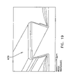
- FIG. 19 is a schematic illustration of a wet etched InP based booster amplifier ridge waveguide
- FIG. 20 is a schematic diagram of a holographic lithography system
- FIG. 21 is a schematic diagram showing a broadband light source configuration with seed wavelength control based on thin-film filters
- FIG. 22 is a schematic diagram showing simulated transmission of a multicavity thin-film notch filter used for seed wavelength control
- FIG. 23 is a schematic diagram showing measured performance obtained using a discrete seed and booster as shown in FIG. 21 for ASE generation.
- FIG. 24 is a schematic diagram showing a measured ASE spectrum at 100 mW of output power from the booster waveguide shown in FIG. 21 .
- a high power broadband light source is used as a high power Raman pump source to facilitate the amplification of optical signals.
- the high power broadband light source is generated from spectrally filtered amplified spontaneous emission (ASE) from various semiconductor or fiber sources.
- ASE amplified spontaneous emission
- a high power broadband light source as a Raman pump source has inherent performance advantages in the areas of gain ripple and flatness, nonlinear pump-to-pump interactions, pump-to-signal interactions, and in the methods of depolarization.
- the excited gain spectrum is a convolution of the pump spectrum and the Raman gain shape shown in FIG. 1 .
- the Raman gain profile ( FIG. 1 ) shows a sharp feature near the peak of the Raman gain. The severity of this feature depends to some extent on the composition of the fiber, and hence on the fiber type.
- pump lasers must be spaced such that the frequency difference between adjacent pumps is less than the bandwidth of the ripple.
- FIG. 5 illustrates the gain profile of a typical design using 6 discrete pump wavelengths distributed across 80 nm. The gain ripple of 0.5 dB is observed. Further reduction of the gain ripple can generally be achieved only if the pump wavelength spacing is reduced to less than 2 nm. Thus, an unfeasibly large number of pump lasers are needed to cover the 80 nm bandwidth.
- the solid curve in FIG. 5 illustrates the results when two broadband pump sources are used to yield a nearly perfectly smooth gain profile.
- the smoothness of the gain ripple is a direct result of the physical convolution “like” process between the pump source spectrum and the Raman response function of the optical fiber.
- the overall flatness of the achieved gain can be controlled by selecting the proper spectral profiles (i.e., wavelength and power distribution) of the broadband pump sources.
- Raman gain is highly polarization dependent. Amplification of the signals is essentially only realized along the same polarization direction as the polarization of the pump. To reduce the polarization-dependent gain, the solution is to provide a depolarized pump source. In current Raman pump modules, this is generally accomplished in one of two ways.
- a depolarizer is used to create two orthogonal linear polarizations.
- This depolarizer may be a passive depolarizer comprising a long length of optical fiber (e.g., ⁇ 10 m), where the single linear polarization state of the high power laser is split into two orthogonal linear components, delayed, and then recombined into one beam.
- the delay length should be greater than the coherence length of the source or an elliptical polarization state will be formed when recombined.
- the long length of the optical fiber depolarizer is necessary when depolarizing a semiconductor laser with an optical fiber depolarizer so as to provide the appropriate delay for the long coherence length of the semiconductor laser.
- FIG. 6 is a schematic diagram of exemplary optical elements, and a pictorial illustration of the polarization state, for depolarizing short and long coherence light sources. The small size of the optical elements and their spacing allows them to be readily integrated into the package of the high power broadband Raman pump source.
- nonlinear optical effects such as Self-phase modulation (SPM), cross-phase modulation (XPM), and four-wave mixing (FWM)
- SPM Self-phase modulation
- XPM cross-phase modulation
- FWM four-wave mixing
- the nonlinear optical interaction can originate from the signal channel as well as from the pump lasers. The relative importance of these effects depends on the particular system design parameters such as power per channel, channel spacing, the total number of channels and fiber dispersion.
- one particularly important nonlinear effect is four-wave mixing between pump lasers. This can be especially detrimental as the amplifier bandwidth approaches the Raman gain peak shift (i.e., ⁇ 100 nm).
- the FWM sidebands on the low frequency (long wavelength) side can fall within the signal window of the frequencies of the amplifier. This effect can be observed in forward, as well as backward, pumped Raman amplifier configurations. In backward pumped configurations (i.e., with signal and pump counter-propagating), the FWM parasitic signal is redirected into the signal direction through Raleigh scattering. If the parasitic FWM signal falls within the receiver bandwidth of a practical signal channel, the quality of the transmission within that channel is seriously degraded.
- the system quality as a whole is limited by the worst case of all the signal channels.
- FIG. 7 illustrates the reduction of FWM achieved in a Raman amplifier pump with a broadband ASE source (see the schematic “b” in FIG. 7 ) as compared to a Raman amplifier pumped with discrete wavelengths (see the schematic “a” in FIG. 7 ).
- linear mechanisms can also be responsible for degradation.
- One such linear mechanism is Raman gain beating which is caused by a coherent beat frequency located between longitudinal modes of a Fabry-Perot laser cavity. For a 1 mm laser cavity length, the mode spacing is approximately 3 angstroms. This corresponds to a 40 GHz coherent beat frequency.
- This coherent beating is particularly detrimental to the noise figure in the forward (i.e., pump and signal co-propagation) Raman amplifier configuration.
- the lack of coherence of the source substantially completely eliminates Raman gain beating.
- the broadband light source used as the Raman pump source can be generated from any light which has a sufficiently broad and intense emission spectrum.
- Such light sources can be formed, for example, from amplified spontaneous emission (ASE) of rare earth doped optical fiber, planar waveguides, or semiconductor optical amplifiers.
- ASE amplified spontaneous emission
- Further examples are spectrally broadened multimode semiconductor lasers or multiorder cascaded Raman lasers. These latter examples (i.e. spectrally broadened multimode semiconductor lasers and multiorder cascaded Raman lasers) have previously been used as Raman pump sources, but with an emphasis on their use for suppressing stimulated Brillouin scattering and, significantly, the spectral broadening is generally limited to no more than a couple of nanometers.
- FIG. 8 illustrates a schematic block diagram of a broadband ASE source in combination with spectral filtering to achieve a desired spectral distribution for the Raman pump.
- Gain profile shaping can be effected by wavelength filtering, within or outside the active devices, in a dynamic or static fashion. Thin-film filters or Bragg gratings can be used for such wavelength filtering.
- the broad optical spectrum can be provided by a single ASE source or a superposition of multiple narrower bandwidth (e.g., 3–40 nm) ASE sources. These narrower bandwidth ASE sources can be multiplexed together in a continuous or discontinuous fashion as illustrated in FIG. 9 so as to form a composite ASE source. In this manner, gain flatness control can be achieved through the control of the total pump spectrum, where total pump spectrum control is in turn achieved through the control of the contribution of the relative intensity of each narrower bandwidth ASE source.
- narrower bandwidth ASE sources can be multiplexed together in a continuous or discontinuous fashion as illustrated in FIG. 9 so as to form a composite ASE source.
- a high power broadband ASE source can also be used for purposes other than Raman amplifiers, e.g., as light sources for general instrumentation (including for example fiberoptic gyros), imaging (including, for example, medical imaging), and semiconductor analysis applications. These applications can benefit since relatively high power can be achieved without the complication of laser speckle resulting from its temporal coherence; however, the waveguide nature of the source provides spatial coherence, thus allowing spatial manipulation of the output as efficiently as a laser beam. Additionally, the relative intensity noise of this source has been shown to be as good as the best semiconductor laser.
- This section describes the semiconductor chip design, fabrication, and packaging considerations for realizing such a device.
- the semiconductor material system used depends to a large extent on the wavelength of the desired application.
- material systems such as AlAs, GaAs, InP, GaP, InGaAs, InGaAsP, InAlGaAs, and GaN can be used.
- the basic principle of device operation is the amplification of a seed spectrum of amplified spontaneous emission (ASE) along the length of a semiconductor waveguide containing one or more active regions which are biased above transparency.
- ASE amplified spontaneous emission
- FIG. 10 is a schematic diagram of a semiconductor die 100 used in a first preferred embodiment.
- the die 100 consists of a serial connection of a wavelength seed section 103 and a power booster or power amplification section 106 formed along a semiconductor waveguide 109 .
- the wavelength seed section 103 preferably comprises multiple subsections 103 A, 103 B, 103 C, etc. formed along the semiconductor waveguide 109 . Three subsections 103 A, 103 B, 103 C are shown in FIG. 10 ; however, it should be appreciated that this number is merely exemplary and more or less than this number of wavelength seed subsections may be used.
- the gain profile within each subsection 103 A, 103 B, 103 C, etc. is chosen so as to provide ASE in a particular wavelength range.
- the gain profiles can be defined in each subsection 103 A, 103 B, 103 C, etc. by such techniques as epitaxial regrowth or quantum well intermixing.
- the quantum well blocks of these subsections are designed to provide a region of high gain with, for example, 3–10 quantum wells.
- a high reflectance mirror 112 is used to capture and redirect the portion of seed light traveling away from the power booster section 106 .
- the spectral profile of this mirror 112 is designed to provide the desired nominal ASE spectrum at the input of the power booster section 106 .
- This high reflectance mirror 112 can be defined through thin film coating of the cleaved semiconductor facet or by incorporating a distributed Bragg reflector along the waveguide.
- Each wavelength seed subsection 103 A, 103 B, 103 C, etc. has an independent electrical contact to allow dynamic tailoring of the seed light spectrum prior to launching into the power booster section 106 .
- the output power of the wavelength seed section 103 can range from 1 to 20 mW, although it is not limited to this range.
- the power booster section 106 is designed to amplify the broad spectrum (20–100 nm) of ASE seed light and generate power in excess of 500 mW. This can be accomplished through the use of a long waveguide section 109 A which is optimized for low loss rather than high gain. Reducing the number of quantum wells to the range of 1 to 5, reducing optical confinement in p-doped cladding, and increasing the confinement factor in n-doped cladding (which has lower free carrier absorption loss) will all reduce the loss. Additionally, the quantum wells must provide gain across the entire wavelength range of the seed light. This can be accomplished through chirping of the thickness of the quantum wells in the vertical direction. For example, the upper quantum well provides shorter wavelength gain while the lower two quantum wells provide longer wavelength gain.
- An angled waveguide 109 B is used at the output of the power booster section 106 , followed by an antireflection coating 115 on the semiconductor facet. This combination is used to eliminate feedback into the power booster section 106 and to prevent distortion of the broadband spectral profile from Fabry-Perot interference.
- the output will be highly linearly polarized because of the polarization dependence of the quantum well gain or, in the case of bulk active region, excess loss of TM over TE mode. If two equal components of linear orthogonal polarization are desired for applications such as Raman amplifiers, the construction described in FIG. 6( b ) can be used.
- the advantages of the construction shown in FIG. 10 include: full semiconductor integration, serial multiplexing, compatibility with dynamic spectral flattening, and reduced packaging complexity, among others.
- FIG. 11 is a schematic diagram of a semiconductor chip 200 and optical train 203 used in a second preferred embodiment. Although multiple chips can be used, this embodiment will be described in the context of a single chip 200 comprising an array of parallel waveguides 206 , where the array comprises a plurality (e.g., 2 to 10) of parallel waveguides 206 A, 206 B, 206 C, etc.
- the gain profile (i.e., peak wavelength and shape) of each waveguide 206 A, 206 B, 206 C, etc. is chosen so as to provide the ASE output in a particular wavelength range (e.g., 3–30 nm).
- the gain profiles can be defined within each waveguide 206 A, 206 B, 206 C, etc. by employing such techniques as epitaxial regrowth, quantum well intermixing or other techniques known in the art.
- the spectral width and intensity of the ASE emitted from each waveguide 206 A, 206 B, 206 C, etc. can be tailored through the design of the active region, the length of the waveguide, and active adjustment of the current injected into each waveguide.
- the quantum well block of each waveguide is designed to provide a region of high gain with, for example, 3–10 quantum wells, along the first 0.3 ⁇ m to 1 mm length of the waveguide.
- the remainder of the waveguide is optimized for low loss rather than high gain so as to amplify the ASE seed light and generate power in excess of 200 mW.
- the number of quantum wells is preferably reduced to the range of, for example, 1 to 5, and the doping in the waveguide cladding can be reduced.
- a high reflectance mirror 209 is provided at one end of the waveguide, and angled waveguides 212 A, 212 B, 212 C, etc. used at the output, followed by a facet antireflection coating 215 . This combination is used to eliminate feedback into the power booster and prevent distortion of the broadband spectral profile from Fabry-Perot interference.
- each waveguide 206 A, 206 B, 206 C, etc. only needs to produce power in a narrower spectral range (e.g., 3–30 nm).
- the power and spectral width of each waveguide 206 A, 206 B, 206 C, etc. are then multiplexed using the optical train 203 contained within the hermetically sealed package.
- the optical train 203 comprises a polarization multiplexer 218 for each pair of waveguides 206 A, 206 B, 206 C, etc., followed by a wavelength multiplexer port 221 for each pair of multiplexers 218 .
- FIG. 11 illustrates this multiplexing principle for 4 waveguides using two polarization multiplexers 218 and a two-port wavelength multiplexer 221 .
- the advantages associated with the construction shown in FIG. 11 include: redundancy, compatibility with dynamic spectral flattening, compatibility with cooler-less operation, and a lower optical power requirement per waveguide, among others.
- FIG. 12 is a schematic diagram of a semiconductor chip 300 and optical train 303 used in a third preferred embodiment.
- the die 306 consists of a wavelength seed section 309 which is power multiplexed by a multiplexer 312 into a long low loss power amplification (or booster) waveguide 315 .
- Wavelength seed section 309 preferably comprises a plurality of wavelength seeds 309 A, 309 B, 309 C, etc. Both the seed light waveguides 309 A, 309 B, 309 C, etc. and the power booster waveguide 315 are designed for broadband ASE emission, just as in the first embodiment ( FIG. 10 ) discussed above.
- a high reflectance mirror is provided for each of the seed waveguides 309 A, 309 B, 309 C, etc.
- the mirrors may be independent of one another, or they may be different sections of a single mirror, such as is shown in FIG. 12 with the high reflectance mirror 318 .
- the reflectivity profiles of the high reflectance mirror for each seed waveguide 309 A, 309 B, 309 C, etc. are optimized to provide the correct seed light profile for control of the output ASE spectrum.
- the power booster waveguide 315 includes an angled end 321 and an anti-reflectance coating 324 at its output end. Spectrum function controls such as tilt can be achieved through the appropriate mix of seed light functions.
- the advantages of the construction shown in FIG. 12 include: redundancy, and reduced control circuit complexity, among others.
- FIG. 13 is a schematic diagram of a semiconductor die 400 and optical train 403 used in a fourth preferred embodiment.
- the semiconductor die 400 consists of an array of, for example, 2 to 10, parallel waveguides 406 A, 406 B, 406 C, etc., each with a narrowband wavelength reflector (e.g., 3–10 nm) to define the seed light bandwidth for each waveguide 406 A, 406 B, 406 C, etc.
- a plurality of discrete reflectors, each formed independent of the others, may be provided; or the reflectors may be different sections of a single reflector, such as is shown in FIG. 13 with the reflector 409 .
- the reflector (as in all of the foregoing embodiments) can be formed, for example, by thin-film deposition, an etched semiconductor distributed Bragg reflector (DBR), or an abutted glass planar light wave guide/grating.
- FIG. 13 illustrates the use of a planar light wave circuit grating to form the reflector 409 .
- the attributes of the power waveguides 406 A, 406 B, 406 C, etc. are substantially the same as disclosed in the second embodiment ( FIG. 11 ) discussed above.
- the outputs of the waveguides 406 A, 406 B, 406 C, etc. are wavelength combined using a thin-film edge-filter multiplexer 412 .
- the multiplexer 412 is preferably formed using a glass substrate 415 with a series of patterned edge-filters 418 deposited by thin film deposition.
- the advantages of the construction shown in FIG. 13 include: compatibility with dynamic spectral flattening, and lower optical power requirement per waveguide, among others.
- FIG. 14 is a schematic diagram of a high power spectrally filtered ASE source 500 which comprises a fifth embodiment of the present invention.
- ASE source 500 comprises a discrete seed 505 and booster 510 which are used to generate high power ASE. More particularly, an isolator 515 is positioned between seed 505 and booster 510 , and a mirror 520 is positioned between isolator 515 and booster 510 .
- a lens 525 is positioned between seed 505 and isolator 515 , a lens 530 is positioned between mirror 520 and booster 510 , and a lens 540 is positioned at the output of booster 510 .
- spectrally filtered ASE light is produced in seed 505 , it is passed through lens 525 and isolator 515 , reflected off mirror 520 , passed through lens 510 and into booster 510 , where it is amplified, and then passed out lens 540 .
- FIG. 15 is a schematic diagram of a spectrally controllable light source device 600 which comprises a sixth embodiment of the present invention.
- Spectrally controllable light source 600 consists of a waveguide seed section 605 which is coupled by a broadband power combiner 610 into a long single-mode high-power “booster” waveguide 615 .
- Waveguide seed section 615 comprises a plurality of wavelength seeds 605 A, 605 B, 605 C, 605 D, etc. Both the seed light waveguides 605 A, 605 B, 605 C, 605 D, etc. and the power booster waveguide 610 are designed for broadband ASE emission, just as in the first embodiment ( FIG. 10 ) discussed above.
- a high reflectance mirror is provided for each of the seed waveguides 605 A, 605 B, 605 C, 605 D, etc. These mirrors may be independent of one another, or they may be different sections of a single mirror, such as is shown in FIG. 15 with the high reflectance mirror 620 .
- the reflectivity profiles of the high reflectance mirror for each seed waveguide 605 A, 605 B, 605 C, 605 D, etc. are optimized to provide the correct seed light profile for control of the output ASE spectrum.
- the power booster waveguide 615 includes an angled end 625 and an anti-reflectance coating 630 at its output end. Spectrum function controls such as tilt can be achieved through the appropriate mix of seed light functions.
- each one of the wavelength seeds 605 A, 605 B, 605 C, 605 D, etc. generate a low power optical seed signal which differ in center wavelength from one another and are approximately 5 nm in spectral width.
- the low power optical seed signals which are preferably in the range of 1–20 mW, are power combined by broadband combiner 610 into long single-mode high-power “booster” waveguide 615 which amplifies the seed signals to higher optical power signals, which are preferably greater than 200 mW.
- the optical output has a single spatial mode and is linearly (TE) polarized, preferably greater than 20 dB.
- the output will exhibit a relative-intensity noise performance rivaling that of a distributed-feedback (DFB) laser ( ⁇ 140 dB/Hz).
- DFB distributed-feedback
- the wavelength seed section 605 of the device 600 is comprised of a parallel array of active semiconductor waveguides 605 A, 605 B, 605 C, 605 D, etc.
- the gain profile within each waveguide is engineered to provide ASE in a particular wavelength range when electrically biased above transparency. It is important to have a high modal gain (both g & ⁇ ) to allow efficient generation of ASE and coupling of the ASE into the waveguide mode for amplification.
- the desired design parameter optimization needed for seed amplifier waveguide 605 A, 605 B, 605 C, 605 D, etc. is similar in nature to that needed for conventional semiconductor optical amplifiers.
- a high reflecting narrowband filter 635 is used to capture, spectrally shape, and redirect the fraction of ASE traveling in the waveguide away from the power booster.
- the spectral profile of mirror 620 is designed to provide the desired center wavelength and spectral width of the ASE spectrum at the input of the power booster waveguide 615 .
- Each wavelength seed section has an independent p-side electrical contact so as to allow dynamic tailoring of the seed light spectrum.
- the output power of the wavelength seed section 605 preferably ranges from 1 to 20 mW.
- the power booster section 615 is designed to amplify the ASE light from seed waveguides 605 A, 605 B, 605 C, 605 D, etc. which generate power in excess of 200 mW.
- the design optimization needed for the power booster 615 is complimentary in nature to that required for high power, i.e., greater than 400 mW, telecomunication lasers. See, for example, (1) Garbuzov D., et al., (2002). 14 xx nm DFB InGaAsP/InP pump lasers with 500 mW CW output power for WDM combining . Optical Fiber Communications Conference, Anaheim, Calif.; and (2) Tsukiji N., et al., (2001).
- Waveguides with a modal loss of less than 2 cm ⁇ 1 are generally utilized. This is accomplished by reducing the number of quantum wells, reducing the optical confinement factor, and utilizing asymmetric confinement where the modal overlap is larger over the n-doped cladding than the p-doped cladding. Additionally, a long cavity reduces the devices voltage drop and allows a lower dopant concentration to be used for reduction of free carrier absorption loss. For example, this cavity may extend several millimeters.
- the quantum wells provide gain across the entire wavelength range of the seed light signals. In a preferred embodiment of the present invention, this is accomplished by chirping the thickness of the quantum wells in the growth direction. For example, the upper quantum well provides shorter wavelength gain while the lower two quantum wells provide longer wavelength gain.
- an angled waveguide 625 is used at the output of the power booster followed by an antireflection coating 630 on the semiconductor facet. This combination is used to reduce feedback into the power booster to less than ⁇ 60 dB and thus prevent distortion of the broadband spectral profile from Fabry Perot interference.
- the output will be highly linearly polarized because of the polarization dependence of the quantum well gain.
- angled waveguide has an angle of about 8°–13°.
- High power ASE is achieved by using discrete seed waveguides 605 A, 605 B, 605 C, 605 D, etc. together with booster amplifier waveguide 615 .
- Device 600 is able to provide ASE power output in excess of 250 mW with a spectral full-width at half-maximum of 20 nm.
- Power combiner 610 is used rather than a wavelength combiner to guide seed light to booster waveguide amplifier 615 for at least two reasons.
- One reason is the tremendously challenging complexity for fabrication of a spectrally flat-top and broadband wavelength multiplexer, such as a multicavity Arrayed Waveguide Grating (AWG).
- Integrated wavelength multiplexing is also unfeasible due to concerns of optical feedback to the seed waveguides as well the large surface area requirements.
- power combiner 610 such as a multimode interferometer (MMI) coupler, is ideal for device 600 in that the MMI has relaxed requirements on the excess loss, broad spectral performance, and provides a high return loss. See, for example, Okamoto, K. (2000). Fundamentals of Optical Waveguides . San Diego, Academic Press.
- MMI multimode interferometer
- Low loss can be achieved in the interference region of MMI though either (1) quantum-well intermixing, (2) epitaxial regrowth, or (3) electrical bias to transparency. See, for example, (1) Holonyak, N. (1998). “Impurity-induced layer disordering of quantum-well heterostructures: discovery and prospects.” IEEE J. Tpcs. Quantum Electron. 4(4) 584–594; (2) Kudo K., et al. (2000). “1.55 ⁇ m wavelength-selectable microarray DBF-LDs with monolithically integrated MMI combiner, SOA, and EA-modulator.” IEEE Photon. Technol. Lett. 12(3); and (3) Hamamato K., et al., (2002). High - power with low electric power consumption 1.45 ⁇ m active multi - mode interferometer laser diode for fiber amplifier applications . Optical Fiber Communications Conference, Anaheim, Calif.
- an approximately 5 nm narrow-band high-reflecting mirror can be created through incorporation of an etched multicavity Bragg reflector along seed waveguide ridge 605 A, 605 B, 605 C, 605 D, etc.
- the multicavity design can be achieved with properly-designed phase masks, which are holographically imprinted on the waveguide directly through standard lithography methods.
- the pattern transfer is preferably achieved through inductively coupled plasma reactive ion etching process.
- wavelength control mechanism 635 for wavelength seeds 605 A, 605 B, 605 C, 605 D, etc. comprises a combination of a series of multicavity narrow-band notch filters 640 A, 640 B, 640 C, 640 D, etc. and high reflectivity feedback mirrors 645 A, 645 B, 645 C, 645 D, etc.
- Multicavity narrow-band notch filters 640 A, 640 B, 640 C, 640 D, etc. are disposed at a 45° angle relative to mirrors 645 A, 645 B, 645 C, 645 D, etc., respectively.
- thin film coatings disposed on mirrors 645 A, 645 B, 645 C, 645 D, etc. are configured to create a 5 nm flat-top transmission peak.
- integrated semiconductor device 600 is capable of generating over 200 mW of fiber coupled power across a spectral range of 1400–1500 nm with 4 or more spectral controls of the emission profile. Each of the spectral controls has 5 nm resolution.
- This preferred embodiment of the present invention relies on multicavity thin-film filters 640 A, 640 B, 640 C, 640 D, etc. for assembly on a micro-optical bench. Specific steps to create this preferred embodiment of the present invention are discussed hereinbelow.
- a first step comprises amplifier waveguide design and growth. This step involves determining the appropriate epitaxy structure through simulation and experiment to provide suitable broadband gain, and high power. A single non-integrated booster and seed waveguide are demonstrated.
- a second step comprises integrated coupler design. This step involves the design of an MMI active/passive (4 ⁇ 1) power combiner for integration with the seeds and booster waveguides. Optical isolation, broadband performance, excess loss, and fabrication methods are simulated.
- a third step comprises integrated coupler growth and fabrication. This step involves the growth, fabrication, and characterization of an (4 ⁇ 1) MMI active/passive coupler.
- a fourth step comprises seed wavelength control. This step encompasses the exploration of various technologies for creating the required narrow-band reflector. Source demonstration may rely on thin-film deposited multi-cavity flat-top 5 nm FWHM bandpass filters.
- a fifth step comprises integration, assembly, and characterization. This step involves taking the results of the previous steps and integrating for demonstration and characterization on a micro-optical bench. Power, Spectral Controllability, and Relative Intensity Noise (RIN) are characterized.
- RIN Relative Intensity Noise
- a fifth step comprises analysis and optimization. This final step involves systematic study of the results and preparation of fully-integrated sources.
- P out spon is the optical power from spontaneous emission
- P heat auger is the power dissipated from nonradiative recombination
- V g is the active region bandgap voltage
- I is the injected current
- l is the incremental (saturated) length of the booster. This equation shows that minimization of the total loss, rather than high gain, is desired.
- the booster waveguide structure can also be used for the seed waveguide structure by increasing the length of the seed. However, this increases die length, and thus effects power consumption, yield, and ultimately cost.
- a chirped quantum well design is employed. This is accomplished through varying the thickness of the quantum wells in the growth direction. For example, the upper quantum well provides shorter wavelength gain while the lower two quantum wells provide longer wavelength gain.
- a solid model will be used for gain curve simulations.
- modal loss in the amplifier waveguide is an important design parameter. Great care is taken to properly optimize this parameter. The impact of reducing doping concentration on voltage should also be considered.
- a technique has been developed to achieve an asymmetric confinement factor. Asymmetric confinement is used to reduce the mode's overlap with the heavily absorptive p-doped region. Booster amplifier waveguides 615 having less than 2 cm ⁇ 1 (total loss) can be achieved using this technique. This technique will further be optimized in a preferred embodiment of the present invention so as to reduce active amplifier waveguide losses for our proposed device to below 1 cm ⁇ 1 .
- FIG. 16 a simulated transverse mode shape 650 of an asymmetric optical confined ridge waveguide 655 of booster waveguide 615 ( FIGS. 15 and 21 ).
- thermal management Often the first limits observed for output power are due to thermal roll over. Finite element techniques may be used to simulate and design the structure's thermal impedance. Looking at FIG. 3 , there is shown a temperature distribution 660 for booster waveguide 615 ( FIGS. 15 and 21 ). The calculated thermal impedance is greater than 7°/W for a 4 mm device.
- An MMI power combiner will be used to guide the light from the seed waveguides to the booster waveguide.
- MMIs have the unique properties of low insertion loss, large optical bandwidth, compact size, polarization insensitivity, low cross talk, and forgiving fabrication tolerances.
- FIG. 18 A design schematic of a typical MMI power combiner 665 is shown in FIG. 18 .
- Optical multimode interference devices based on self-imaging principles and applications.” J. Lightwave Technol. 13:615–627) the dimensions of the MMI as shown in FIG. 18 are chosen to satisfy self-imaging.
- the influence of waveguide loss on coupler performance are extensively parameterized. This result together with the outcome of the fabrication considerations of the step comprising the integrated coupler growth and fabrication determine the final MMI design.
- substeps are performed to complete the integrated coupler design. These substeps include simulation/calculation using BPM, FDTD, and analytic techniques of the excess loss, return loss to seed and booster, spectral dependence of the coupling coefficient, and output mode shape. The substeps also comprise parameterization of the effect of waveguide loss and finalization of dimensions and layer structure using considerations from the step of the integrated coupler growth and fabrication.
- the MMI coupler 665 will be grown in the InP/InGaAsP material system using a MOCVD. Coupler 665 is preferably fabricated using conventional wafer processing techniques. Coupler 665 is fabricated using InP-baged materials through optical lithography and wet/dry etching processes. Referring now to FIG. 19 , there is shown a wet-etched InP based ridge waveguide 670 in a SEM micrograph.
- the interference region of the MMI 665 must have low loss. This presents challenges in achieving the integration of the active seed waveguides 605 and booster waveguides 615 with power combiner 610 , such as MMI 665 . There are two approaches for achieving low loss. These include quantum-well intermixing, see Holonyak, N. (1998). “Impurity-induced layer disordering of quantum-well heterostructures: discovery and prospects.” IEEE J. Sel. Tpcs. Quantum Electron. 4(4):584–594, and electrical bias to transparency, see Hamamoto K., et al., (2002). High power with low electric power consumption 1.45 ⁇ m active multi - mode interferometer laser diode for fiber amplifier applications . Optical Fiber Communications Conference, Anaheim, Calif.
- the selection of the approach is made through analysis of the simulation results of the integrated coupler design together with the results of initial intermixing experiments.
- Intermixing can be used for spatial bandgap tuning of multiquantum well structures, see, for example, Si, S. K., et al., (1998). “Area selectivity of InGaAsP-InP multiquantum-well intermixing by impurity-free vacancy diffusion.” IEEE J. Sel. Tpcs. Quant. Elect. 4(4) 619–623. Impurity-free vacancy diffusion (IFVD) benefits from low scattering loss, see Si, S. K., et al., (1998). “Area selectivity of InGaAsP—InP multiquantum-well intermixing by impurity-free vacancy diffusion.” IEEE J. Sel. Tpcs. Quant. Elect. 4(4) 619–623.
- Vacancy intermixing can be achieved through implantation of double-charged phosphorus ions (P++) in the layers above the quantum well active region. See, for example, Paquette, M. et al. (1998). Blueshifting of InGaAsP-InP laser diodes using a low energy ion-implantation technique.” IEEE J. Sel. Tpcs. Quant. Elect. 4(4): 741–745. Point defects are generated that are able to thermally diffuse and contribute to intermixing when annealed. The bandgap of the resulting intermixed material shifts to higher energy by more than 80 nm, i.e., near 1480 nm.
- the intermixed material exhibits similar photoluminescence intensity to that of the non-implanted material.
- Lasers with excellent slope efficiency and threshold have been fabricated using intermixed material. See, for example, Paquette, M. et al. (1998). Blueshifting of InGaAsP—InP laser diodes using a low energy ion-implantation technique.” IEEE J. Sel. Tpcs. Quant. Elect. 4(4): 741–745; and Yu, S. F., et al. (1998). “Semiconductor lasers using diffused quantum-well structures.” IEEE J. Sel. Tpcs. Quant. Elect. 4(4): 723–735. This method of vacancy diffusion is utilized for shifting the bandgap in the interference region of the MMI to avoid optical absorption.
- One substep is fabrication of waveguide lasers with intermixed material. This is followed by evaluation of the internal loss and the internal quantum efficiency. A freeze fabrication approach may also be used.
- narrow-band, high-reflecting mirror 620 is created by incorporating a multicavity Bragg reflector etched along the ridge of seed waveguide 605 A, 605 B, 605 C, 605 D, etc.
- the multicavity design is achieved with a properly-designed phase mask, holographically imprinted on the waveguide 605 A, 605 B, 605 C, 605 D, etc. through standard lithography methods.
- the pattern transfer can be achieved through an inductively-coupled-plasma reactive-ion-etching process.
- FIG. 20 there is shown a holographic lithography technique 675 .
- a Karl Suss MA6 lithography system is fitted with a near field holographic adapter to create holographic lithography technique 675 .
- the 0 beam 680 and ⁇ 1 beam 685 are used to create interference patterns 690 on waveguides 605 A, 605 B, 605 C, 605 D, etc.
- the 0/ ⁇ 1 order principle is advantageous for fine-pitch applications that require suppression of unwanted orders.
- incident light 695 is diffracted partially into the ⁇ 1 order 685 .
- Self-interference between the ⁇ 1 order 685 and the undiffracted zero order beam 680 creates an interference pattern 690 with a pitch equal to the phase mask pitch.
- This approach is advantageous over conventional +1/ ⁇ 1 order phase mask as +1 order beam can degrade the grating formation, and hence influence its optical characteristics.
- holographic grating technique 675 is implemented for “on-chip” wavelength control for further scaling of the number of seed guides 605 .
- This relies on the use of external thin-film filters 640 A, 640 B, 640 C, 640 D, etc. for wavelength control of seeds 605 A, 605 B, 605 C, 605 D, etc., respectively.
- Dielectric notch filters 640 A, 640 B, 640 C, 640 D, etc. and high reflecting feedback mirrors 645 A, 645 B, 645 C, 645 D, etc. are used in combination with one another, respectively.
- the multi-cavity and high reflective thin films can be deposited by an Ion Tech Spector ion beam sputtering system.
- An optical monitoring system ensures accurate coatings to meet the technical requirements.
- Proper glass substrate ensures athermal properties of the coating.
- Multicavity thin notch filters 640 A, 640 B, 640 C, 640 D, etc. are designed as a narrow band filter about 5 nm wide and centered at 1450 nm.
- substeps are preferably performed for creating seed wavelength control. These substeps include the evaluation of the holographic imprinting technique for etching of multicavity semiconductor Bragg gratings, the design and deposit thin-film filters for off-chip wavelength control, and the provision of prototype thin-film wavelength control of a single seed waveguide.
- Integration and assembly of device 600 occurs after (1) amplifier waveguide design and growth, (2) integrated coupler design, (3) integrated coupler growth and fabrication, and (4) seed wavelength control.
- Seed array 605 is first fabricated with MMI coupler 610 and output of MMI 610 is characterized for power, mode shape, spectral distribution, and RIN. Information from these measurements is then used to feedback and iterate the process where required.
- Booster 615 is then fabricated after MMI 610 .
- the semiconductor die 705 is then be bonded to an AlN carrier and actively aligned on an AlN platform to lens array 710 and thin film filters 640 A, 640 B, 640 C, 640 D, etc. The optical performance is then tested.
- substeps are preferably performed during integration, assembly and characterization. These substeps include fabrication of seed array 605 with MMI coupler 610 ; characterization of performance of device 600 , including power, mode shape, spectral distribution, & RIN; and iteratation of the process/design as required. Next, these substeps include fabrication of a complete device 600 and characterization of its performance by assembling it together with thin-film filters for stabilization on micro-optical bench, and then characterization of device 600 performance including power, mode shape, spectral distribution, & RIN.
- non-integrated seed and booster amplifier waveguides are used to generate high power ASE.
- the seed wavelength generated by discrete seed 505 is not controlled by a spectral filter nor are the active regions of the amplifier waveguides engineered to provide an extended gain bandwidth of greater than 50 nm as described in this preferred embodiment of the present invention.
- the output ASE power in this preferred embodiment of the present invention is nearly three times higher than the highest known report achieved from a single-mode semiconductor waveguide (see, for example, Cho, S. H., et al. (2001) “90 mW CW superluminescent output power from single-angled facet-ridge waveguide at 1.5 ⁇ m.” Trends in Optics and Photonics Series 31) and more than ten times that of any comparable commercial product (e.g., several telecommunication instrumentation suppliers market broadband single-mode fiber-coupled semiconductor LED sources for use in passive WDM component characterization with output powers in the range of 0 to 10 mW).
- FIG. 23 there is shown a plot 715 of the measured light-verses-current performance obtained using device 600 having a discrete seed array 605 and booster 615 for ASE generation.
- more than 250 mW of ASE power is generated by the ASE source 500 .
- the seed input power is approximately 3 mW and the measured ASE spectrum has a full-width half-maximum (FWHM) of 20 nm.
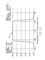
- FIG. 24 there is shown the measured ASE spectrum 720 from booster waveguide 615 at 100 mW of output power. Similar spectra output is produced at the maximum output power.
- the RIN spectrum of this source is less than ⁇ 140 dB/Hz from 100 Hz to beyond 15 GHz.
- a system and method have been disclosed for amplifying optical signals such as those used in telecommunication systems, HFC-CATV applications, and other instrumentation and imaging applications.
- a system and method for producing a high power broadband light source from ASE have also been disclosed, where the high power broadband light source may be used for amplifying optical signals or for other purposes, e.g., general instrumentation (including, for example, fiberoptic gyros), imaging (including, for example, medical imaging, and semiconductor analysis applications). While various preferred embodiments have been described and shown, it will be understood that there is no intent to limit the present invention by such disclosure but, rather, it is intended to cover all modifications and alternate constructions falling within the spirit and scope of the invention.
Abstract
Description
where β is the spontaneous emission factor, Γ is the optical confinement factor, g is the material gain, I is the injected current, and l is the seed's length. Large modal gain and and a high spontaneous emission factor are desirable. For the booster waveguide, the limiting maximum power is given by,
where η is the internal quantum efficiency,
is the optical power from spontaneous emission,
is the power dissipated from nonradiative recombination, Vg is the active region bandgap voltage, I is the injected current, and l is the incremental (saturated) length of the booster. This equation shows that minimization of the total loss, rather than high gain, is desired.
Claims (14)
Priority Applications (1)
| Application Number | Priority Date | Filing Date | Title |
|---|---|---|---|
| US10/758,343 US7190861B2 (en) | 2003-01-15 | 2004-01-15 | Monolithic semiconductor light source with spectral controllability |
Applications Claiming Priority (3)
| Application Number | Priority Date | Filing Date | Title |
|---|---|---|---|
| US44011503P | 2003-01-15 | 2003-01-15 | |
| US10/632,779 US7215836B2 (en) | 2002-08-02 | 2003-08-01 | System for amplifying optical signals |
| US10/758,343 US7190861B2 (en) | 2003-01-15 | 2004-01-15 | Monolithic semiconductor light source with spectral controllability |
Related Parent Applications (1)
| Application Number | Title | Priority Date | Filing Date |
|---|---|---|---|
| US10/632,779 Continuation-In-Part US7215836B2 (en) | 2002-08-02 | 2003-08-01 | System for amplifying optical signals |
Publications (2)
| Publication Number | Publication Date |
|---|---|
| US20050201675A1 US20050201675A1 (en) | 2005-09-15 |
| US7190861B2 true US7190861B2 (en) | 2007-03-13 |
Family
ID=34922584
Family Applications (1)
| Application Number | Title | Priority Date | Filing Date |
|---|---|---|---|
| US10/758,343 Expired - Fee Related US7190861B2 (en) | 2003-01-15 | 2004-01-15 | Monolithic semiconductor light source with spectral controllability |
Country Status (1)
| Country | Link |
|---|---|
| US (1) | US7190861B2 (en) |
Cited By (10)
| Publication number | Priority date | Publication date | Assignee | Title |
|---|---|---|---|---|
| US20090014646A1 (en) * | 2006-02-13 | 2009-01-15 | Daryoosh Vakhshoori | Method and apparatus for incorporating electrostatic concentrators and/or ion mobility separators with Raman, IR, UV, XRF, LIF and LIBS spectroscopy and /or other spectroscopic techniques |
| US20090237647A1 (en) * | 2007-05-21 | 2009-09-24 | Masud Azimi | Preparing samples for optical measurement |
| US20100315629A1 (en) * | 2009-06-15 | 2010-12-16 | Knopp Kevin J | Optical Scanning |
| US8248588B2 (en) | 2007-05-21 | 2012-08-21 | Thermo Scientific Portable Analytical Instruments Inc. | Handheld infrared and raman measurement devices and methods |
| US20170085322A1 (en) * | 2015-09-23 | 2017-03-23 | Fujitsu Limited | Harmonic generation and phase sensitive amplification using a bragg reflection waveguide |
| US10050414B2 (en) | 2015-01-22 | 2018-08-14 | Hewlett Packard Enterprise Development Lp | Monolithic WDM VCSEL arrays by quantum well intermixing |
| RU2688962C1 (en) * | 2018-05-30 | 2019-05-23 | федеральное государственное автономное образовательное учреждение высшего образования "Санкт-Петербургский национальный исследовательский университет информационных технологий, механики и оптики" (Университет ИТМО) | Method of stabilizing parameters of output optical radiation of strong spontaneous emission source |
| US10868407B2 (en) | 2015-06-04 | 2020-12-15 | Hewlett Packard Enterprise Development Lp | Monolithic WDM VCSELS with spatially varying gain peak and fabry perot wavelength |
| US10938175B2 (en) | 2015-05-13 | 2021-03-02 | Furukawa Electric Co., Ltd. | Light source for Raman amplification, light source system for Raman amplification, Raman amplifier, and Raman amplifying system |
| WO2022054860A1 (en) | 2020-09-09 | 2022-03-17 | 古河電気工業株式会社 | Light source, light source device, method for driving light source, raman amplifier, and raman amplification system |
Families Citing this family (13)
| Publication number | Priority date | Publication date | Assignee | Title |
|---|---|---|---|---|
| KR100559469B1 (en) * | 2003-06-09 | 2006-03-10 | 한국전자통신연구원 | Gain-clamped optical amplifier |
| KR100575966B1 (en) * | 2003-12-18 | 2006-05-02 | 삼성전자주식회사 | Broadband light source |
| KR20050070566A (en) * | 2003-12-30 | 2005-07-07 | 삼성전자주식회사 | Multi-wavelength light source and wavelength-division multiplexing system using the same |
| GB2419033B (en) * | 2004-10-08 | 2009-12-09 | Agilent Technologies Inc | An integrated modulator / laser assembly and a method of producing same |
| US7702201B2 (en) * | 2006-06-08 | 2010-04-20 | Industrial Technology Research Institute | Gain flattening utilizing a two-stage erbium-based amplifier |
| CN101373318B (en) * | 2007-08-22 | 2011-06-22 | 鸿富锦精密工业(深圳)有限公司 | Projection system |
| JP5545752B2 (en) * | 2010-12-20 | 2014-07-09 | 富士通テレコムネットワークス株式会社 | Optical packet switching system |
| US9025241B2 (en) * | 2011-10-14 | 2015-05-05 | Kotura, Inc. | Gain medium providing laser and amplifier functionality to optical device |
| KR20140092214A (en) * | 2013-01-15 | 2014-07-23 | 오므론 가부시키가이샤 | Laser oscillator |
| JP6508956B2 (en) * | 2015-01-28 | 2019-05-08 | 富士通株式会社 | Modulated light source |
| CN106663916B (en) * | 2015-02-12 | 2020-09-25 | 古河电气工业株式会社 | Semiconductor laser device |
| WO2016182068A1 (en) * | 2015-05-13 | 2016-11-17 | 古河電気工業株式会社 | Light source for raman amplification, light source system for raman amplification, raman amplifier, raman amplifying system |
| GB2580956B (en) * | 2019-01-31 | 2023-01-25 | Exalos Ag | Amplified Spontaneous Emission Semiconductor Source |
Citations (8)
| Publication number | Priority date | Publication date | Assignee | Title |
|---|---|---|---|---|
| US6038239A (en) * | 1995-04-20 | 2000-03-14 | Gabbert; Manfred | Tunable alignment-stable laser light source having a spectrally filtered exit |
| US6212310B1 (en) | 1996-10-22 | 2001-04-03 | Sdl, Inc. | High power fiber gain media system achieved through power scaling via multiplexing |
| US6292288B1 (en) | 1998-07-23 | 2001-09-18 | The Furukawa Electric Co., Ltd. | Raman amplifier, optical repeater, and raman amplification method |
| US6522465B1 (en) | 2001-09-27 | 2003-02-18 | Intel Corporation | Transmitting spectral filtering of high power extreme ultra-violet radiation |
| US6542287B1 (en) | 2000-12-12 | 2003-04-01 | Onetta, Inc. | Optical amplifier systems with transient control |
| US6693740B2 (en) | 2001-08-07 | 2004-02-17 | Corning Incorporated | Dispersion managed discrete Raman amplifiers |
| US6697558B2 (en) | 2000-03-03 | 2004-02-24 | Fitel U.S.A. Corp | Raman amplified optical system with reduction of four-wave mixing effects |
| US6731426B2 (en) | 2001-02-23 | 2004-05-04 | Photon-X, Inc. | Long wavelength optical amplifier |
-
2004
- 2004-01-15 US US10/758,343 patent/US7190861B2/en not_active Expired - Fee Related
Patent Citations (8)
| Publication number | Priority date | Publication date | Assignee | Title |
|---|---|---|---|---|
| US6038239A (en) * | 1995-04-20 | 2000-03-14 | Gabbert; Manfred | Tunable alignment-stable laser light source having a spectrally filtered exit |
| US6212310B1 (en) | 1996-10-22 | 2001-04-03 | Sdl, Inc. | High power fiber gain media system achieved through power scaling via multiplexing |
| US6292288B1 (en) | 1998-07-23 | 2001-09-18 | The Furukawa Electric Co., Ltd. | Raman amplifier, optical repeater, and raman amplification method |
| US6697558B2 (en) | 2000-03-03 | 2004-02-24 | Fitel U.S.A. Corp | Raman amplified optical system with reduction of four-wave mixing effects |
| US6542287B1 (en) | 2000-12-12 | 2003-04-01 | Onetta, Inc. | Optical amplifier systems with transient control |
| US6731426B2 (en) | 2001-02-23 | 2004-05-04 | Photon-X, Inc. | Long wavelength optical amplifier |
| US6693740B2 (en) | 2001-08-07 | 2004-02-17 | Corning Incorporated | Dispersion managed discrete Raman amplifiers |
| US6522465B1 (en) | 2001-09-27 | 2003-02-18 | Intel Corporation | Transmitting spectral filtering of high power extreme ultra-violet radiation |
Non-Patent Citations (17)
| Title |
|---|
| Agrawal et al., Nonlinear Fiber Optics, 1989, Ch.8, Academic Press. |
| Cho et al., 90 mW CW Superluminescent Output Power from Single-Angled Facet-Ridge Waveguide at 1.5 um, Trends in Optics and Photonics Series, 2001, 31. |
| Fludger et al., Pump to Signal RIN Transfer in Raman Fiber Amplifiers, Journal of Lightwave Technology, Aug. 2001, 1140-1148, 19(8). |
| Garbuzov et al., 14xx nm DFB InGaAsP/InP Pump Lasers with 500 mW CW Output Power for WDM Combining, Optical Fiber Communications Conference, 2002, Anaheim, CA. |
| Hamamoto et al., High Power with Low Electric Power Consumption 1.45 um Active Multi-Mode Interferometer Laser Diode for Fiber Amplifier Applications, Optical Fiber Communications Conference, 2002, Anaheim, CA. |
| Harder et al, "High-Power Ridge-Waveguide AIGaAs GRINSCH Laser Diode", published in the Electronics Letters of Sep. 25, 1986 vol. 22, No. 20, pp. 1081-1082. * |
| Holonyak, Impurity-Induced Layer Disordering of Quantum-Well Heterostructures: Discovery and Prospects, IEEE Journal of Selected Topics in Quantum Electronics, Jul./Aug. 1998, 584-594, 4(4). |
| Kidorf et al., Pump Interactions in a 100-nm Bandwidth Raman Amplifier, IEEE Photonics Technology Letters, May 1999, 530-32, 11(5). |
| Koch et al., Broadband Raman Gain Characterisation in Various Optical Fibers, Electronics Letters, Nov. 22, 2001, 1437-1439, 37(24). |
| Kudo et al., 1.55 um Wavelength-Selectable Microarray DFB-LD's with Monolithically Integrated MMI Combiner, SOA, and EA-Modulater, IEEE Photonics Technology Letters, Mar. 2000, 12 (3). |
| Matsushita et al., Design of Temperature Insensitive Depolarizer for Raman Pump Laser Diode, OSA Technical Digest, OFC2002, WB3. |
| Okamoto, Fundamentals of Optical Waveguides, 2000, Academic Press, San Diego. |
| Paquette et al., Blueshifting of InGaAsP-InP Laser Diodes Using a Low Energy Ion-Implantation Technique: Comparison Between Strained and Lattice-Matched Quantum-Well Structures, IEEE Journal of Selected Topics in Quantum Electronics, Jul./Aug. 1998, 741-745, 4(4). |
| Si et al., Area Selectivity of InGaAsP-InP Multiquantum-Well Intermixing by Impurity-Free Vacancy Diffusion, IEEE Journal of Selected Topics in Quantum Electronics, Jul./Aug. 1998, 619-623, 4(4). |
| Soldano et al., Optical Multi-Mode Interference Devices Based on Self-Imaging: Principles and Applications, Journal of Lightwave Technology, Apr. 1995, 615-627, 13(4). |
| Tsukiji et al., Recent Progress of High Power 14XX nm Pump Lasers, SPIE ITcom on Active and Passive Optical Components for WDM Communication, 2001, Denver, CO. |
| Yu et al., Semiconductor Lasers Using Diffused Quantum-Well Structures, IEEE Journal of Selected Topics in Quantum Electronics, Jul./Aug. 1998, 723-735, 4(4). |
Cited By (17)
| Publication number | Priority date | Publication date | Assignee | Title |
|---|---|---|---|---|
| US7838825B2 (en) | 2006-02-13 | 2010-11-23 | Ahura Scientific Inc. | Method and apparatus for incorporating electrostatic concentrators and/or ion mobility separators with Raman, IR, UV, XRF, LIF and LIBS spectroscopy and/or other spectroscopic techniques |
| US20090014646A1 (en) * | 2006-02-13 | 2009-01-15 | Daryoosh Vakhshoori | Method and apparatus for incorporating electrostatic concentrators and/or ion mobility separators with Raman, IR, UV, XRF, LIF and LIBS spectroscopy and /or other spectroscopic techniques |
| US8248588B2 (en) | 2007-05-21 | 2012-08-21 | Thermo Scientific Portable Analytical Instruments Inc. | Handheld infrared and raman measurement devices and methods |
| US20090237647A1 (en) * | 2007-05-21 | 2009-09-24 | Masud Azimi | Preparing samples for optical measurement |
| US8081305B2 (en) | 2007-05-21 | 2011-12-20 | Ahura Scientific Inc. | Preparing samples for optical measurement |
| US9841371B2 (en) | 2009-06-15 | 2017-12-12 | Thermo Scientific Portable Analytical Instruments Inc. | System for determining a composition of a sample using wavelength dependent variability measurement with multiple time intervals |
| US8891086B2 (en) | 2009-06-15 | 2014-11-18 | Thermo Scientific Portable Analytical Instruments Inc. | Optical scanning systems and methods for measuring a sealed container with a layer for reducing diffusive scattering |
| US20100315629A1 (en) * | 2009-06-15 | 2010-12-16 | Knopp Kevin J | Optical Scanning |
| US10050414B2 (en) | 2015-01-22 | 2018-08-14 | Hewlett Packard Enterprise Development Lp | Monolithic WDM VCSEL arrays by quantum well intermixing |
| US10938175B2 (en) | 2015-05-13 | 2021-03-02 | Furukawa Electric Co., Ltd. | Light source for Raman amplification, light source system for Raman amplification, Raman amplifier, and Raman amplifying system |
| US11652329B2 (en) | 2015-05-13 | 2023-05-16 | Furukawa Electric Co., Ltd. | Light source for Raman amplification, light source system for Raman amplification, Raman amplifier, and Raman amplifying system |
| US10868407B2 (en) | 2015-06-04 | 2020-12-15 | Hewlett Packard Enterprise Development Lp | Monolithic WDM VCSELS with spatially varying gain peak and fabry perot wavelength |
| US20170085322A1 (en) * | 2015-09-23 | 2017-03-23 | Fujitsu Limited | Harmonic generation and phase sensitive amplification using a bragg reflection waveguide |
| US9923634B2 (en) * | 2015-09-23 | 2018-03-20 | Fujitsu Limited | Harmonic generation and phase sensitive amplification using a bragg reflection waveguide |
| US10256911B2 (en) * | 2015-09-23 | 2019-04-09 | Fujitsu Limited | Harmonic generation and phase sensitive amplification using a bragg reflection waveguide |
| RU2688962C1 (en) * | 2018-05-30 | 2019-05-23 | федеральное государственное автономное образовательное учреждение высшего образования "Санкт-Петербургский национальный исследовательский университет информационных технологий, механики и оптики" (Университет ИТМО) | Method of stabilizing parameters of output optical radiation of strong spontaneous emission source |
| WO2022054860A1 (en) | 2020-09-09 | 2022-03-17 | 古河電気工業株式会社 | Light source, light source device, method for driving light source, raman amplifier, and raman amplification system |
Also Published As
| Publication number | Publication date |
|---|---|
| US20050201675A1 (en) | 2005-09-15 |
Similar Documents
| Publication | Publication Date | Title |
|---|---|---|
| US7190861B2 (en) | Monolithic semiconductor light source with spectral controllability | |
| Zimmerman et al. | Amplifiers for the masses: EDFA, EDWA, and SOA amplets for metro and access applications | |
| US7215836B2 (en) | System for amplifying optical signals | |
| US6433921B1 (en) | Multiwavelength pumps for raman amplifier systems | |
| US5721636A (en) | Laser pumping of erbium amplifier | |
| Verdier et al. | Ultrawideband wavelength-tunable hybrid external-cavity lasers | |
| US6680960B2 (en) | Semiconductor laser device having a diffraction grating on a light emission side | |
| EP0952472A2 (en) | Optical functional element and transmission device | |
| US7769062B2 (en) | Quantum dot based semiconductor waveguide devices | |
| US6947463B2 (en) | Semiconductor laser device for use in a laser module | |
| US6614823B2 (en) | Semiconductor laser device having a diffraction grating on a light reflection side | |
| US20030021314A1 (en) | Distributed bragg reflector semiconductor laser suitable for use in an optical amplifier | |
| JP2019083351A (en) | Semiconductor optical amplifier, semiconductor laser module, and wavelength-variable laser assembly | |
| JP2001085800A (en) | Semiconductor optical amplifier module, and, optical communication system | |
| US20030064537A1 (en) | Semiconductor laser device and method for effectively reducing facet reflectivity | |
| Akrout et al. | Error-free transmission of 8 WDM channels at 10 Gbit/s using comb generation in a quantum dash based mode-locked laser | |
| Stephens et al. | Low-input power wavelength conversion at 10 Gb/s using an integrated amplifier/DFB laser and subsequent transmission over 375 km of fiber | |
| Yin et al. | Laser diode comb spectrum amplification preserving low RIN for WDM applications | |
| SATO et al. | Semiconductor Optical Amplifier and Gain Chip Used in Wavelength Tunable Lasers | |
| Ketelsen et al. | 2.5 Gb/s transmission over 680 km using a fully stabilized 20 channel DBR laser with monolithically integrated semiconductor optical amplifier, photodetector and electroabsorption modulator | |
| US10938183B2 (en) | Wavelength-variable laser | |
| JP3752171B2 (en) | Semiconductor laser device, semiconductor laser module, and Raman amplifier using the same | |
| Suzuki et al. | Tunable distributed reflector lasers combined by monolithically integrated AWG coupler | |
| Kang et al. | A single to multi-wavelength converter using Fabry–Perot laser diode with linear optical amplifier and its applications to the wavelength division multiplexing-passive optical network system | |
| Takaki et al. | High-power CW-DFB LDs for optical communications |
Legal Events
| Date | Code | Title | Description |
|---|---|---|---|
| AS | Assignment |
Owner name: AHURA CORPORATION, MASSACHUSETTS Free format text: ASSIGNMENT OF ASSIGNORS INTEREST;ASSIGNORS:KNOPP, KEVIN J.;VAKHSHOORI, DARYOOSH;WANG, PEIDONG;REEL/FRAME:019010/0888 Effective date: 20070213 |
|
| FEPP | Fee payment procedure |
Free format text: PAYOR NUMBER ASSIGNED (ORIGINAL EVENT CODE: ASPN); ENTITY STATUS OF PATENT OWNER: LARGE ENTITY |
|
| CC | Certificate of correction | ||
| FEPP | Fee payment procedure |
Free format text: PAT HOLDER NO LONGER CLAIMS SMALL ENTITY STATUS, ENTITY STATUS SET TO UNDISCOUNTED (ORIGINAL EVENT CODE: STOL); ENTITY STATUS OF PATENT OWNER: LARGE ENTITY |
|
| FPAY | Fee payment |
Year of fee payment: 4 |
|
| FEPP | Fee payment procedure |
Free format text: PAYOR NUMBER ASSIGNED (ORIGINAL EVENT CODE: ASPN); ENTITY STATUS OF PATENT OWNER: LARGE ENTITY Free format text: PAYER NUMBER DE-ASSIGNED (ORIGINAL EVENT CODE: RMPN); ENTITY STATUS OF PATENT OWNER: LARGE ENTITY |
|
| FEPP | Fee payment procedure |
Free format text: PAYOR NUMBER ASSIGNED (ORIGINAL EVENT CODE: ASPN); ENTITY STATUS OF PATENT OWNER: LARGE ENTITY Free format text: PAYER NUMBER DE-ASSIGNED (ORIGINAL EVENT CODE: RMPN); ENTITY STATUS OF PATENT OWNER: LARGE ENTITY |
|
| REMI | Maintenance fee reminder mailed | ||
| LAPS | Lapse for failure to pay maintenance fees | ||
| STCH | Information on status: patent discontinuation |
Free format text: PATENT EXPIRED DUE TO NONPAYMENT OF MAINTENANCE FEES UNDER 37 CFR 1.362 |
|
| FP | Lapsed due to failure to pay maintenance fee |
Effective date: 20150313 |