US7191380B2 - Defect-tolerant and fault-tolerant circuit interconnections - Google Patents
Defect-tolerant and fault-tolerant circuit interconnections Download PDFInfo
- Publication number
- US7191380B2 US7191380B2 US10/659,892 US65989203A US7191380B2 US 7191380 B2 US7191380 B2 US 7191380B2 US 65989203 A US65989203 A US 65989203A US 7191380 B2 US7191380 B2 US 7191380B2
- Authority
- US
- United States
- Prior art keywords
- signal lines
- coded
- address signal
- addresses
- input
- Prior art date
- Legal status (The legal status is an assumption and is not a legal conclusion. Google has not performed a legal analysis and makes no representation as to the accuracy of the status listed.)
- Active, expires
Links
Images


Classifications
-
- G—PHYSICS
- G06—COMPUTING; CALCULATING OR COUNTING
- G06F—ELECTRIC DIGITAL DATA PROCESSING
- G06F11/00—Error detection; Error correction; Monitoring
- G06F11/07—Responding to the occurrence of a fault, e.g. fault tolerance
- G06F11/08—Error detection or correction by redundancy in data representation, e.g. by using checking codes
- G06F11/10—Adding special bits or symbols to the coded information, e.g. parity check, casting out 9's or 11's
- G06F11/1008—Adding special bits or symbols to the coded information, e.g. parity check, casting out 9's or 11's in individual solid state devices
- G06F11/1012—Adding special bits or symbols to the coded information, e.g. parity check, casting out 9's or 11's in individual solid state devices using codes or arrangements adapted for a specific type of error
- G06F11/1016—Error in accessing a memory location, i.e. addressing error
-
- B—PERFORMING OPERATIONS; TRANSPORTING
- B82—NANOTECHNOLOGY
- B82Y—SPECIFIC USES OR APPLICATIONS OF NANOSTRUCTURES; MEASUREMENT OR ANALYSIS OF NANOSTRUCTURES; MANUFACTURE OR TREATMENT OF NANOSTRUCTURES
- B82Y10/00—Nanotechnology for information processing, storage or transmission, e.g. quantum computing or single electron logic
-
- G—PHYSICS
- G11—INFORMATION STORAGE
- G11C—STATIC STORES
- G11C13/00—Digital stores characterised by the use of storage elements not covered by groups G11C11/00, G11C23/00, or G11C25/00
- G11C13/0002—Digital stores characterised by the use of storage elements not covered by groups G11C11/00, G11C23/00, or G11C25/00 using resistive RAM [RRAM] elements
- G11C13/0009—RRAM elements whose operation depends upon chemical change
- G11C13/0014—RRAM elements whose operation depends upon chemical change comprising cells based on organic memory material
-
- G—PHYSICS
- G11—INFORMATION STORAGE
- G11C—STATIC STORES
- G11C8/00—Arrangements for selecting an address in a digital store
- G11C8/10—Decoders
-
- G—PHYSICS
- G11—INFORMATION STORAGE
- G11C—STATIC STORES
- G11C2213/00—Indexing scheme relating to G11C13/00 for features not covered by this group
- G11C2213/70—Resistive array aspects
- G11C2213/77—Array wherein the memory element being directly connected to the bit lines and word lines without any access device being used
-
- G—PHYSICS
- G11—INFORMATION STORAGE
- G11C—STATIC STORES
- G11C2213/00—Indexing scheme relating to G11C13/00 for features not covered by this group
- G11C2213/70—Resistive array aspects
- G11C2213/81—Array wherein the array conductors, e.g. word lines, bit lines, are made of nanowires
Definitions
- the present invention relates to nanoscale electronic circuits and, in particular, to defect-tolerant interconnection interfaces with electrically distinguishable signal levels, including interfaces between microelectronic and nanoelectronic circuits used in a combination nanoscale/microscale electronic memory, combination nanoscale/microscale logic circuits, field-programmable gate arrays, and processors.
- the present invention is related to nanoscale electronic circuit interconnections, including memory devices employing nanowire crossbars and defect-tolerant interconnections with electrically distinguishable signal levels between microelectronic circuit elements and nanowires.
- Nanowire crossbar technologies and a variety of nanoscale electronic circuits, are discussed in a number of issued U.S. patents and filed U.S. patent applications, including (1) U.S. Pat. No. 6,459,095, entitled “Chemically Synthesized and Assembled Electronic Devices,” issued to James R. Heath et al. on Oct. 1, 2002; (2) U.S. Pat. No. 6,314,019, entitled “Molecular Wire Crossbar Interconnect (MWCI) for Signal Routing and Communications,” issued to Philip J. Kuekes et al.
- MWCI Molecular Wire Crossbar Interconnect
- Nanowire crossbars provide an enormous increase in device density compared with current, photolithography-produced microelectronic and sub-microelectronic circuitry.
- many alignment and spontaneous defect problems need to be overcome to successfully manufacture electronic devices that include nanoelectronic circuits, including nanowire crossbars.
- a number of techniques and nanowire-crossbar implementations have been designed to overcome these alignment and defect problems, including configurable, or reprogrammable, nanowire-crossbar implementations that allow defects to be detected and circumvented by programming configurations that provide desired functionality without incorporating defective molecular junctions.
- microelectronic circuitry produced by photolithographic techniques, because microelectronic circuits can be assumed, in the current discussion, to be essentially perfect or, more precisely, the defect rate in photolithography-produced microelectronic circuits is so far below the current defect rate in nanoscale electronic circuitry that the comparatively very low defect rate in microelectronic circuitry can be ignored.
- Nanoscale electronic circuits need to interface to microelectronic circuitry in order to be incorporated within commercially viable and useful electronic devices.
- the interface between essentially non-defective microelectronic circuitry and nanoelectronic circuitry is problematic. While various correctly functioning nanoelectronic circuits can be configured from defect-prone nanowire crossbars, these nanoscale circuits need to be interconnected with microelectronic circuits.
- the relatively high manufacturing-defect rate that occurs in fabricating nanoelectronic devices may produce a yield of usable combination nanoscale/microscale circuits too low to be economically viable.
- redundancy-based, defect avoidance strategies designed for nanoscale circuits to microelectronic circuitry through nanoscale-to-microscale interfaces because these redundancy-based techniques depend on an ability to attempt a measurement of each junction in the nanoscale circuits to determine whether or not the junction is defective.
- Such individual access to junctions within an interconnection interface would require the interconnection interface to be properly functioning in the first place.
- the redundancy-based techniques assume defective nanoscale circuitry components, but rely on an ability to address the components through a properly working interconnection interface.
- defects in the interconnection interface result in degradation or complete lack of addressability of interconnection interface components.
- the interconnection interface may be viewed as a type of bootstrap mechanism that allows defect control in a nanoscale circuit, the components of which are addressed through the bootstrap
- electronic memories based on nanowire-crossbar-implemented memory-element arrays are attractive with respect to size and power consumption, but are not economically viable using current designs and manufacturing strategies, because defects in the interconnect would make large portions of the memory unaddressable, pushing the effective cost/bit of manufacture to a level too high to be competitive.
- the selected nanowire is designed to have a low, “0,” or, synonymously, OFF state, and the unselected nanowires are designed to have a high, “1,” or, synonymously, ON state, then the voltage or current difference between the selected nanowire and the lowest voltage or lowest current unselected nanowire must be sufficiently large to be easily detected.
- the electronic characteristics of nanowire molecular junctions may be difficult to precisely manufacture, leading to leaky diodes, resistors with a wide variation in resistance, and leaky transistors, in turn leading to undesirably narrow differences between ON and OFF states in addressed nanowires.
- nanoscale electronic circuitry and, in particular, nanoscale electronic memories, have recognized the need for defect-tolerant interconnection within nanoscale circuitry in the interface between microscale and nanoscale circuits.
- designers and manufacturers of nanoscale electronic circuitry have recognized the need for interconnections with distinguishable signal levels between nanowires and address signal lines that select one or a subset of nanowires to have a different voltage or current state than the remaining nanowires.
- One embodiment of the present invention is an electronic memory comprising an array of nanowire crossbars, the nanoscale memory elements within the nanowire crossbars addressed through conventional microelectronic address lines.
- an address encoding technique is employed to generate a number of redundant address lines to supplement a minimally required set of address signal lines needed to access the nanoscale memory elements.
- the supplemental address lines allow for unique memory-element addressing in the presence of significant nanowire-to-microelectronic-address-line interconnection defects, provided that the functional interrelationships between the supplemental address lines and the minimally required set of address lines are properly constrained.
- the functional interrelationships may be mathematically specified using generator matrices originally derived for error-control coding used in data transmission, or may be specified using combinatoric codes or random codes.
- the supplemental address signal lines serve to increase the voltage or current separation between selected nanowires and non-selected nanowires when a particular address is input to the address signal lines in order to select one, or a subset of, the nanowires.
- nanocomponent addresses are input to an encoder that outputs corresponding coded addresses by using encoding techniques that increase the average Hamming-distance separation of the coded addresses with respect to the average Hamming-distance separation of the nanocomponent addresses.
- nanocomponent addresses input to an encoder are encoded into coded addresses by encoding techniques that increase the minimum Hamming-distance separation of the coded addresses with respect to the minimum Hamming-distance separation of the nanocomponent addresses.
- the methods of the present invention are applicable to a wide range of different types of systems in which a signal level is classified as belonging to one of a plurality of different, distinguishable classes based on one or more thresholds separating the signal-level classes.
- Systems to which the methods of the present invention are applicable include microfluidics-based systems, which may depend on chemical-signal thresholds for which precise manufacture, detection, and operation may be problematic. Additional examples include microelectromechanical (“MEMS”) systems, hybrid electrical systems featuring nanoscale, microscale, and macroscale components, and quantum computing.
- MEMS microelectromechanical
- FIG. 1 shows a high-level diagram of a combined nanoscale/microscale electronic memory device that represents one embodiment of the present invention.
- FIG. 2 shows an abstract representation of a nanowire-crossbar memory-element subarray within a combined nanoscale/microscale electronic memory device.
- FIGS. 3A–B shows a simple nanoscale-to-microscale interface within a combined nanoscale/microscale electronic memory device.
- FIGS. 4A–D illustrate voltages on the horizontal nanowires resulting from four possible signal patterns input to the internal microelectronic address signal lines in the nanoscale interconnection interface illustrated in FIGS. 3A–B .
- FIG. 5 shows a table indicating voltage states of nanowires resulting from address signals input to microelectronic address signal lines of a nanoscale interconnection interface.
- FIG. 6 shows the nanoscale interconnection interface discussed above with reference to FIG. 3A–4D with a failed rectifying connection.
- FIGS. 7A–D using the same illustration conventions of FIGS. 4A–D , illustrate voltage states of nanowires that arise with each different, two-bit signal pattern input to the address signal lines.
- FIG. 8 shows a table indicating voltage states of nanowires resulting from address signals input to microelectronic address signal lines of a nanoscale interconnection interface, using the same illustration conventions as used in FIG. 5 , for the defective nanoscale interconnection interface illustrated in FIGS. 6–7D .
- FIG. 9 illustrates a nanoscale interconnection interface in which two rectifying interconnections are defective.
- FIG. 10 shows a table indicating voltage states of nanowires resulting from address signals input to microelectronic address signal lines of a nanoscale interconnection interface, using the same illustration conventions as used in FIGS. 5 and 8 , for the defective nanoscale interconnection interface illustrated in FIG. 9 .
- FIG. 11 shows a modified nanoscale interconnection interface, similar to the interconnect interfaces illustrated in FIGS. 3A–4D , that represents one embodiment of the present invention.
- FIGS. 12A–D illustrate nanowire voltage states arising from input of four different, two-bit addresses to the address signal lines of the nanoscale interconnection interface, representing one embodiment of the present invention, shown in FIG. 11 .
- FIG. 13 shows a table indicating voltage states of nanowires resulting from address signals input to microelectronic address signal lines of a nanoscale interconnection interface, using the same illustration conventions as used in FIGS. 5 , 8 , and 10 , for the defective nanoscale interconnection interface illustrated in FIGS. 11–12D .
- FIG. 14 shows the modified nanoscale interconnection interface shown in FIG. 11 , representing one embodiment of the present invention, with a single defective rectifying interconnect.
- FIGS. 15A–D analogous to FIGS. 12A–D , show voltage states of nanowires arising from four different, two-bit addresses input to the address signal lines.
- FIG. 16 shows a table indicating voltage states of nanowires resulting from address signals input to microelectronic address signal lines of a nanoscale interconnection interface, using the same illustration conventions as used in FIGS. 5 , 8 , 10 , and 13 , for the defective, modified nanoscale interconnection interface illustrated in FIGS. 14–15D .
- FIG. 17 shows the modified nanoscale interconnection interface first shown in FIG. 11 with two defective rectifying connections.
- FIG. 18 shows a table indicating voltage states of nanowires resulting from address signals input to microelectronic address signal lines of a nanoscale interconnection interface, using the same illustration conventions as used in FIGS. 5 , 8 , 10 , 13 , and 16 , for the defective, modified nanoscale interconnection interface illustrated in FIG. 17 .
- FIG. 19 shows a defective, modified nanoscale interconnection interface similar to that shown in FIG. 11 , representing one embodiment of the present invention, but having three defective rectifying connections.
- FIG. 20 shows a table indicating voltage states of nanowires resulting from address signals input to microelectronic address signal lines of a nanoscale interconnection interface, using the same illustration conventions as used in FIGS. 5 , 8 , 10 , 13 , and 16 , for the defective, modified nanoscale interconnection interface illustrated in FIG. 17 .
- FIGS. 21 and 22 illustrate loss of unique addressability in the modified nanoscale interconnection interface, which involves the loss of two connections from microwires to one nanowire
- FIGS. 23A–B illustrate the comparative robustness of two-bit addresses and three-bit addresses in the nanoscale interconnection interfaces discussed with respect to FIGS. 3A–22 .
- FIGS. 24A–B illustrate address-space topologies of the two-bit, fully occupied address space and a three-bit, sparsely occupied address space.
- FIG. 25 illustrates a generalized technique for providing parity-check address signal lines via an encoder component in order to increase the defect-tolerance and fault-tolerance of nanoscale interconnection interfaces that represents one embodiment of the present invention.
- FIGS. 26A–B illustrate the derivation of an encoding circuit that adds parity-check address signal lines to an incoming set of address signal lines and derivation of a demultiplexer corresponding to the encoding circuit that both represent embodiments of the present invention.
- FIG. 27 shows a plot of the normalized expected number of addressable bits per unit area plotted against the defect rate for a 16K-bit cross-point memory using no supplemental address signal lines and using a number of different linear-block codes for specifying different numbers of supplemental address signal lines.
- FIG. 28 shows plots of an expected addressable percentage of nanowires versus a probability of open connections for a nanoscale interconnection interface having no supplemental address signal lines and nanoscale interconnection interfaces designed using various linear block codes to specify different numbers of supplemental address signal lines.
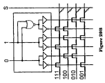
- FIG. 29A illustrates a diode-based demultiplexer, similar to demultiplexers illustrated in previous figures that represent embodiments of the present invention.
- FIG. 29B illustrates a transistor-based demultiplexer, equivalent to the demultiplexer illustrated in FIG. 29A , that represents an embodiment of the present invention.
- Various embodiments of the present invention include a combined nanoscale/microscale electronic memory device and fault-tolerant interconnections between microelectronic circuits and nanoelectronic circuits within the electronic memory.
- Techniques for determining, in one described approach, nanoelectronic-to-microelectronic interface topologies employ concepts and mathematical techniques developed for error-control coding used in various data-transmission applications. Therefore, in a first subsection, a mathematical description of a number of error-control encoding techniques is provided. In a second subsection, a partially nanoscale electronic memory that represents one embodiment of the present invention is described. In a third subsection, a method for determining the nanoelectronic-to-microelectronic circuit-interface topologies within the electronic memory are described.
- Embodiments of the present invention employ concepts derived from well-known techniques in error-control encoding.
- An excellent reference for this field is the textbook “Error Control Coding: The Fundamentals and Applications,” Lin and Costello, Prentice-Hall, Incorporated, New Jersey, 1983.
- This subsection a brief description of the error-detection and error-correction techniques used in error-control encoding are described. Additional details can be obtained from the above-referenced textbook, or from many other textbooks, papers, and journal articles in this field.
- the current subsection represents a rather mathematically precise, but concise, description of certain types of error-control encoding techniques.
- the current invention employs concepts inherent in these error-control encoding techniques for a different purpose.
- Error-control encoding techniques systematically introduce supplemental bits or symbols into plain-text messages, or encode plain-text messages using a greater number of bits or symbols than absolutely required, in order to provide information in encoded messages to allow for errors arising in storage or transmission to be detected and, in some cases, corrected.
- One effect of the supplemental or more-than-absolutely-needed bits or symbols is to increase the distance between valid codewords, when codewords are viewed as vectors in a vector space and the distance between codewords is a metric derived from the vector subtraction of the codewords.
- the current invention employs concepts used in error-control coding to add supplemental address signal lines to increase the distance between valid addresses in order to correspondingly increase the signal separation, e.g.
- the plain-text and encoded messages of error-control encoding are analogous to input addresses and coded addresses, and the additional or greater-number-than-needed symbols or bits in error-control encoding are analogous to supplemental or a greater-than-absolutely-needed number of address signal lines.
- a message ⁇ comprises an ordered sequence of symbols, ⁇ i , that are elements of a field F.
- the field F is a set that is closed under multiplication and addition, and that includes multiplicative and additive inverses. It is common, in computational error detection and correction, to employ fields comprising a subset of integers with sizes equal to a prime number, with the addition and multiplication operators defined as modulo addition and modulo multiplication. In practice, the binary field is commonly employed.
- Block encoding techniques encode data in blocks.
- a block can be viewed as a message u comprising a fixed number of symbols k that is encoded into a message c comprising an ordered sequence of n symbols.
- the encoded message c generally contains a greater number of symbols than the original message ⁇ , and therefore n is greater than k.
- the r extra symbols in the encoded message where r equals n ⁇ k, are used to carry redundant check information to allow for errors that arise during transmission, storage, and retrieval to be detected with an extremely high probability of detection and, in many cases, corrected.
- the 2 k codewords form a k-dimensional subspace of the vector space of all n-tuples over the field F.
- the Hamming weight of a codeword is the number of non-zero elements in the codeword, and the Hamming distance between two codewords is the number of elements in which the two codewords differ. For example, consider the following two codewords a and b, assuming elements from the binary field:
- the encoding of data for transmission, storage, and retrieval, and subsequent decoding of the encoded data can be notationally described as follows, when no errors arise during the transmission, storage, and retrieval of the data: ⁇ c ( s ) ⁇ c ( r ) ⁇ where c(s) is the encoded message prior to transmission, and c(r) is the initially retrieved or received, message.
- an initial message ⁇ is encoded to produce encoded message c(s) which is then transmitted, stored, or transmitted and stored, and is then subsequently retrieved or received as initially received message c(r).
- the initially received message c(r) is then decoded to produce the original message ⁇ .
- the originally encoded message c(s) is equal to the initially received message c(r), and the initially received message c(r) is straightforwardly decoded, without error correction, to the original message ⁇ .
- message encoding and decoding can be expressed as follows: ⁇ ( s ) ⁇ c ( s ) ⁇ c ( r ) ⁇ ( r )
- the final message ⁇ r may or may not be equal to the initial message ⁇ (s), depending on the fidelity of the error detection and error correction techniques employed to encode the original message ⁇ (s) and decode or reconstruct the initially received message c(r) to produce the final received message ⁇ (r).
- Error detection is the process of determining that: c ( r ) ⁇ c ( s ) while error correction is a process that reconstructs the initial, encoded message from a corrupted initially received message: c ( r ) ⁇ c ( s )
- the encoding process is a process by which messages, symbolized as ⁇ , are transformed into encoded messages c.
- a messages ⁇ can be considered to be a word comprising an ordered set of symbols from the alphabet consisting of elements of F
- the encoded messages c can be considered to be a codeword also comprising an ordered set of symbols from the alphabet of elements of F.
- a word ⁇ can be any ordered combination of k symbols selected from the elements of F
- a codeword c is defined as an ordered sequence of n symbols selected from elements of F via the encoding process: ⁇ c: ⁇ c ⁇
- the generator matrix G for a linear block code can have the form:
- G k , n ( p 0 , 0 p 0 , 1 ⁇ p 0 , r - 1 1 0 0 ⁇ 0 p 1 , 0 p 1 , 1 ⁇ p 1 , r - 1 0 1 0 ⁇ 0 . . ⁇ 0 ⁇ 0 1 ⁇ 0 . . ⁇ . . . ⁇ .
- the generator matrix G can be placed into a form of a matrix P augmented with a k by k identity matrix I k,k .
- a code generated by a generator in this form is referred to as a “systematic code.”
- the codewords comprise r parity-check symbols c i followed by the symbols comprising the original word ⁇ .
- the original word, or message ⁇ occurs in clear-text form within, and is easily extracted from, the corresponding codeword.
- the parity-check symbols turn out to be linear combinations of the symbols of the original message, or word ⁇ .
- H r,n [I r,r
- H r , n ( 1 0 0 ⁇ 0 - p 0 , 0 - p 1 , 0 - p 2 , 0 ⁇ - p k - 1 , 0 0 1 0 ⁇ 0 - p 0 , 1 - p 1 , 1 - p 2 , 1 ⁇ - p k - 1 , 1 0 0 1 ⁇ 0 - p 0 , 2 - p 1 , 2 - p 2 , 2 ⁇ - p k - 1 , 2 . . . ⁇ .
- H T ( 1 0 0 ⁇ 0 0 1 0 ⁇ 0 0 0 1 ⁇ 0 . . . ⁇ 1 - p 0 , 0 - p 0 , 1 - p 0 , 2 ⁇ - p 0 , r - 1 - p 1 , 0 - p 0 , 1 - p 0 , 2 ⁇ - p 0 , r - 1 - p 2 , 0 - p 0 , 1 - p 0 , 2 ⁇ - p 0 , r - 1 . 0 , 2 ⁇ - p 0 , r - 1 . . . ⁇ .
- Q] where I m is an m ⁇ m identity matrix and the submatrix Q comprises all 2 m ⁇ m ⁇ 1 distinct columns which are m-tuples each having 2 or more non-zero elements. For example, for m 3, a parity-check matrix for a [7,4,3] linear block Hamming code is
- one embodiment of the present invention involves employing the above-described error-control coding techniques to a very different problem space, in which, rather than generating codewords of length k+r from messages of length k, interconnections between k+r internal signal lines are generated from addresses input into k input signal lines.
- one embodiment of the present invention involves applying error-control coding techniques to addresses within an address space of size 2 k to generate interconnection mappings between address signal lines and up to 2 k signal lines addressed by the 2 k addresses.
- the additional symbols or bits are parity-check symbols or bits that supplement the plain-text symbols or bits, while in the other types of codes, valid messages are distributed throughout a vector space of dimension equal to the codeword size.
- supplemental address lines refers to either parity-check address signal lines, analogous to parity-check symbols or bits in linear block codes, or to the greater-number-than-absolutely-needed address signal lines, analogous to the greater-number-than-needed symbols or bits in these other types of codes.
- these other codes may have different advantages that provide utility in different applications.
- Combinatoric codes provide a straightforward approach to increasing the Hamming distance between codewords.
- a combinatoric code also known as a “constant-weight code” or an “r-hot code”
- r-hot code a combinatoric code
- Random code Another, similar type of code, referred to as a “random” code, is obtained by choosing random codewords of fixed length. For example, one can choose a fixed-length, binary, n-bit codeword size, and select a sufficient number of random n-bit binary numbers in order to obtain a desired number of binary codewords 2 k , where n>Ak. The greater the value of A, the greater the expected minimum Hamming distance between the codewords.
- distance checking can be carried out to reject new codewords that have a Hamming distance less than a minimum value with respect to those codewords already selected, and random codewords having approximately equal numbers of “1” and “0” bits can be used in order to obtain an increased average Hamming distance and increased expected minimum Hamming distance.
- a random linear code is a type of code that may be employed in the methods and systems of the present invention.
- the generator matrix is randomly generated, under linearity constraints, rather than generated as the combination of a parity-check matrix generated from linear sums of information elements that represent parity-check sums, and an identity matrix.
- a random linear block code is generally not systematic, but linear.
- codes that may be employed in the methods and systems of the present invention may be systematic and linear, systematic and non-linear, non-systematic and linear, or non-systematic and non-linear.
- C is a code
- u is an arbitrary n-vector
- C′ is another code with the same distance properties, and hence with the same error correction and defect tolerance capabilities.
- C is linear, and u is non-zero
- C′ is non-linear, technically, an affine space.
- the random codes are generally neither systematic nor linear.
- linear block codes have properties that are attractive in the applications to be discussed below, linear codes, systematic codes, and non-linear, non-systematic codes may also be employed in various embodiments of the present invention.
- nanoscale/microscale electronic memory device that represents one embodiment of the present invention is discussed.
- the present invention is not limited in applicability to nanoscale/microscale electronic memory devices, or even to nanoscale/microscale electronic devices, but may also find application in purely nanoscale interconnection interfaces and other nanoscale devices, and may also find application in sub-microscale electronic devices, interconnection interfaces, and memories.
- single nanowires are uniquely addressed by addresses transmitted to intersecting microscale address signal lines.
- subsets of nanowires may be addressed, rather than single nanowires, by a single address.
- the present invention is related to general addressing of components within a circuit, and not limited to uniquely addressing single components or signal lines, nor limited to components or signal lines of particular sizes.
- FIG. 1 shows a high-level diagram of a combined nanoscale/microscale electronic memory device that represents one embodiment of the present invention.
- the combined nanoscale/microscale electronic memory device 100 interfaces to an external electronic environment through reference voltage signal lines 102 and through two sets of address signal lines 104 and 106 .
- the memory elements within the combined nanoscale/microscale electronic memory device 100 can logically be considered to compose a two-dimensional array, with each memory element specified by a pair of coordinates (x,y), where the x coordinate specifies the row of the two-dimensional array inhabited by the memory element and the y coordinate specifies the column of the two-dimensional array inhabited by the memory element.
- the set of address signal lines 106 may be used to specify one of 2 p two-dimensional memory-element-array rows, where p is the number of address signal lines in the set of address signal lines 106 , and the set of address signal lines 104 specifies one of 2 q columns in the logical, two-dimensional array of memory elements, where q is the number of address signal lines in the set of address signal lines 106 .
- p and q of the two-dimensional array of memory elements need not be equal, in the following discussion, both dimensions will be assumed to be equal to p, in the interest of notational brevity.
- the external sets of address signal lines 104 and 106 are electronically used within the electronic memory device 100 to select a column and row of nanowire-crossbar memory-element subarrays, and therefore a particular nanowire-crossbar memory-element subarray, and to select a particular row or column within a selected nanowire-crossbar array.
- the upper three address signal lines 108 of the set of address signal lines 106 may specify one of seven horizontal rows 110 – 116 of nanowire-crossbar subarrays
- the upper three address signal lines 118 of the set of address signal lines 104 may specify one of six vertical columns 120 – 125 of nanowire crossbar memory-element subarrays.
- the lower three address signal lines 126 in the set of address signal lines 106 specify a particular row of nanoscale memory elements within a selected nanowire-crossbar memory-element subarray
- the lower three address signal lines 128 in the set of address signal lines 104 specifies a particular column of nanoscale memory elements within a selected nanowire-crossbar memory-element subarray. Note that, in general, a larger number of input address signal lines would be employed to address a larger number of columns and rows of nanowire-crossbar memory-element subarrays than shown in FIG. 1 , as well as a larger number of nanoscale-memory-element rows and columns within each nanowire-crossbar memory-element subarray. The small number of input address lines shown in FIG. 1 is chosen for illustration convenience only.
- Each row and column of nanowire-crossbar memory-element subarrays is accessed through an encoder 130 – 142 .
- the encoder receives, in FIG. 1 , the high-order three input address signal lines and outputs a larger number of coded address signal lines.
- encoder 137 receives three address signal lines 144 directly interconnected with the high-order input address signal lines 128 , and outputs five coded address signal lines 146 .
- the address signal lines output by an encoder pass through all of the nanowire-crossbar memory-element subarrays within the column or row accessed via the encoder.
- the five coded address signal lines 146 output by the encoder 137 pass through nanowire-crossbar memory-element subarrays 150 – 156 .
- Each nanowire-crossbar memory-element subarray is also connected to two reference voltage signal lines.
- nanowire-crossbar memory-element subarray 150 is connected to the reference voltage through reference-voltage signal lines 158 and 160 .
- the input address signal lines may be microscale address signal lines, or may have even larger dimensions.
- the coded address signal lines are generally microelectronic or submicroelectronic signal lines produced by currently available photolithographic techniques.
- the nanowire-crossbar memory-element subarrays are composed of nanoscale wires, or nanowires. Nanowires have cross-sectional diameters of less than 100 nanometers, while submicroelectronic signal lines have cross-sectional diameters of greater than 100 nanometers. Therefore, there are two nanoscale interconnection interfaces within each nanowire-crossbar memory-element subarray.
- the circuitry within the encoders 130 – 142 is significantly more complex than the circuitry within the nanowire-crossbar memory-element subarrays.
- each encoder provides access to an entire row or column of nanowire-crossbar memory-element subarrays, thus amortizing the complexity of the encoders over an often large number of nanowire-crossbar memory-element subarrays.
- defect and fault-tolerant nanoscale interconnection interfaces are facilitated by the supplemental address signal lines output by each encoder.
- FIG. 2 shows an abstract representation of a nanowire-crossbar memory-element subarray within a combined nanoscale/microscale electronic memory device.
- the nanowire-crossbar memory-element subarray 200 is composed of a nanowire crossbar 202 with a similarly sized region 204 of horizontally extending nanowires and a similarly sized region 206 of vertically extending nanowires.
- a vertical column 208 of microelectronic coded address signal lines passes over the region of horizontally extending nanowires 204 , with selective rectifying connections, or nanoscale, molecular-junction diode connections, interconnecting microelectronic internal signal lines with particular horizontal extending nanowires.
- resistive ohmic connections, semi-conductor gate connections, or other types of physical methods at nanowire junctions that determine the signals on the nanowires 204 may be employed.
- a horizontal set 210 of microelectronic coded address signal lines passes over the region 206 of vertically extending nanowires, with the horizontal microelectronic address signal lines selectively interconnected via rectifying connections, or molecular diodes, to selected vertically extending nanowires.
- each horizontally and vertically extended nanowire is also connected, through a resistive connection, to a vertical reference-voltage signal line 212 and a horizontal reference-voltage signal line 214 , respectively.
- Each unique pattern of ON and OFF voltages, or, equivalently, HIGH and LOW voltages, on the set of vertical internal microelectronic address signal lines 208 uniquely addresses a particular, horizontally extending nanowire, and places that selected nanowire at a significantly different voltage than the remaining horizontally extending nanowires.
- each different pattern of ON and OFF voltages on the set 210 of horizontal internal microelectronic address signal lines selects a unique vertically extending nanowire, and places that selected vertically extending nanowire at a significantly different voltage than the remaining vertically extending nanowires.
- the selected horizontally extending nanowire and the selected vertically extending nanowire are interconnected at a single crossover point within the nanowire crossbar, and the molecular junction at that crossover point is placed at a different voltage level than all other molecular junctions within the nanowire crossbar via the pattern of ON and OFF voltages present on the set of vertical and horizontal internal microelectronic signal lines 208 and 210 .
- FIG. 3A shows a simple nanoscale-to-microscale interface within a combined nanoscale/microscale electronic memory device.
- two internal microelectronic signal lines 302 and 304 pass over and selectively interconnect with four nanowires 306 – 309 .
- Each nanowire 306 – 309 is interconnected to a reference-voltage microelectronic signal line 310 via a resistive interconnection 312 – 315 , respectively. Note that each nanowire has been assigned a two-bit address.
- Nanowire 306 has the address “00,” nanowire 307 has the address “01,” nanowire 308 has the address “10,” and nanowire 309 has the address “11.”
- each internal microelectronic signal line 302 and 304 is split into a complementary pair.
- internal microelectronic address signal line 302 passes over the nanowires as a pair of microelectronic signal lines 316 – 317 , with the right-hand microelectronic signal line 316 of the pair having the same voltage as the internal microelectronic signal line 302 , and the left-hand microelectronic signal line 317 of the pair having a voltage complementary to that of the internal microelectronic address signal line 302 .
- FIG. 3B shows the selective rectifying crosspoint connections between the complementary-pair, microelectronic address signal lines 316 – 317 and 318 – 319 and the four nanowires 306 – 309 .
- each rectifying connection is indicated by a diagonally directed diode symbol, such as diagonally directed diode symbol 320 .
- Those crosspoints, or intersections, without diagonally directed diode schematics are not electrically interconnected.
- coded signal line refers, in this document, to either a single coded signal line or to a complementary pair of signal lines.
- various formulas and expressions are provided that are related to the number of coded signal lines in particular implementations or used in particular techniques. If, for example, a formula or expression refers to n coded signal lines, then n refers to the number of independent signal lines or to the number of independent, complementary pairs of signal lines. In certain implementations, single, independent coded signal lines may be employed. In other implementations, including the implementations discussed in this document, complementary pairs of signal are employed.
- FIGS. 4A–D illustrate voltages on the horizontal nanowires resulting from four possible signal patterns input to the internal microelectronic address signal lines in the nanoscale interconnection interface illustrated in FIGS. 3A–B .
- the voltage V for a nanowire can be computed from the following formula:
- V A and V B are the voltages of the relatively high-voltage-signal-carrying internal address signal lines, at a given point in time, connected to the nanowires of interest, e.g. internal address signal lines 317 and 319 for nanowire 309 at the point in time illustrated in FIG.
- V S is the source voltage
- the resistance R S is the resistance of the resistor interconnecting reference-voltage signal line 310 with the nanowire
- the resistances R A and R B are the effective resistances of the forward-biased or reverse biased rectifying connections, depending on the voltages on the connected address signal lines, if the nanowire is interconnected with the internal microelectronic address signal lines.
- the address-signal-line voltage pattern “00” is input into the internal, microelectronic address signal lines 302 and 304 .
- the complement microelectronic signal lines 317 and 319 are held at a high voltage V H while the direct address signal lines of the complementary pairs 316 and 318 are held at essentially 0 volts.
- the reference-voltage signal line 310 is also held at 0 volts.
- the address signal lines held at high voltage are indicated by arrows, such as arrow 322 , drawn within the address signal line.
- Horizontal nanowire 309 receives high voltage input from both complementary address signal lines 317 and 319 , resulting in a voltage of 0.95 V H .
- Each of the horizontal nanowires 307 and 308 receives a single high voltage input from one of the two complementary address signal lines 317 and 319 .
- Horizontal nanowire 306 receives no high voltage input, and is therefore held at the reference voltage zero by the reference-voltage signal line 310 .
- the address “00” input to the internal, microelectronic address signal lines 302 and 304 results in selection of nanowire “00” 306 for a low voltage state, and a high voltage state held on the remaining three horizontal nanowires 307 – 309 .
- FIG. 5 shows a table indicating voltage states of nanowires resulting from address signals input to microelectronic address signal lines of a nanoscale interconnection interface.
- the nanowire addresses are shown on a vertical axis 502 and the address signals input to the microelectronic address signal lines are shown on a horizontal axis 504 .
- the table clearly reveals that a single nanowire is held at low voltage for each different address, and that the address input to the internal, microelectronic address signal lines is equal to the address assigned to the selected nanowire.
- microscale-to-nanoscale demultiplexer interface discussed above with reference to FIGS. 3A–4D is fabricated with rectifying connections, or molecular diodes, interconnecting the address signal lines with the nanowires.
- non-rectifying, resistive connections may be employed, with resistances substantially less than the resistance of the resistor interconnecting the nanowires with the reference-voltage signal line.
- resistive interconnections rather than diode interconnections, the voltage differences between the selected, low-voltage nanowire and the remaining nanowires may be significantly less when a similar high voltage V H is applied to selected address signal lines.
- the difference in the voltages of the non-selected nanowires in the above example is small, 0.05 volts
- the voltage states of the non-selected nanowires in a resistive connection implementation span a much larger range.
- FIG. 6 shows the nanoscale interconnection interface discussed above with reference to FIG. 3A–4D with a failed rectifying connection.
- the rectifying connection interconnecting address signal line 318 with horizontal nanowire 307 is missing, leaving the crosspoint between the address signal line 318 and the nanowire 307 in a permanent open state.
- the nanoscale interconnections cannot, with current technologies, be as reliably fabricated as can interconnections in microscale electronics fabricated using photolithographic processes.
- FIGS. 7A–D using the same illustration conventions of FIGS. 4A–D , illustrate voltage states of nanowires that arise with each different, two-bit signal pattern input to the address signal lines.
- the lack of the rectifying connection (indicated by dashed circle 602 in FIG. 6 ) results in an inability to uniquely address nanowire “11” 309 .
- FIG. 8 shows a table indicating voltage states of nanowires resulting from address signals input to microelectronic address signal lines of a nanoscale interconnection interface, using the same illustration conventions as used in FIG. 5 , for the defective nanoscale interconnection interface illustrated in FIGS. 6–7D . Comparing FIG.
- nanowire “11” 309 cannot be uniquely addressed, as indicated by the two zero voltage states 802 and 804 in the column 806 corresponding to input signal “11.” However, an additional effect may be observed.
- FIG. 5 there is a descending, right diagonal of 0.95 V H voltage states, while in FIG. 8 , voltage state 808 for nanowire “ 01 ” with input signal “10” is now 0.90 V H , rather than 0.95 V H .
- the failed rectifying connection has also lowered the cumulative voltage difference between the selected-nanowire, low-voltage state and the high voltage states of the unselected nanowires.
- FIG. 9 illustrates a nanoscale interconnection interface in which two rectifying interconnections are defective.
- the two defective rectifying interconnections are illustrated in FIG. 9 by dashed circles 902 and 904 .
- FIG. 10 shows a table indicating voltage states of nanowires resulting from address signals input to microelectronic address signal lines of a nanoscale interconnection interface, using the same illustration conventions as used in FIGS. 5 and 8 , for the defective nanoscale interconnection interface illustrated in FIG. 9 .
- Comparison of FIG. 10 to FIGS. 5 and 8 show that the additional failed rectifying connection ( 904 in FIG. 9 ) has further degraded the nanoscale interconnection interface. Now, only nanowire “00” can be uniquely addressed.
- input of the signal pattern “10” selects both nanowires “10” and “11,” as indicated by the zero voltage states shown in cells 1002 and 1004 .
- nanowire “01” is selected both by address signal pattern “01” and by signal pattern “11,” as indicated by the zero voltage states in cells 1006 and 1010 .
- there are now only two maximum voltage states shown in cells 1012 and 1014 rather than four maximum voltage states shown in the rightward descending diagonal in FIG. 5 .
- FIG. 11 shows a modified nanoscale interconnection interface, similar to the interconnect interfaces illustrated in FIGS. 3A–4D , that represents one embodiment of the present invention.
- the modified nanoscale interconnection interface 1100 has four addressable nanowires 1102 – 1105 with two-bit addresses “00,” “01,” “10,” and “11,” as in the interconnection interface shown in FIG. 3A .
- the modified interconnection interface also employs two address signal lines 1106 and 1107 into which two-bit addresses may be input. As in the previously described interconnection interface, shown in FIG. 3A , each address signal line 1106 and 1107 is split into a complementary pair, 1108 – 1109 and 1110 – 1111 , respectively. However, an additional complementary pair of signal lines 1112 and 1113 , with signals derived from the signals input to the address signal lines 1106 and 1107 , are also selectively interconnected to the nanowires 1102 – 1105 via rectifying nanoscale connections, such as rectifying nanoscale connection 1114 .
- the complementary signal-line pair 1112 – 1113 represents a parity-check signal line, derived from the address signal lines 1106 – 1107 by an inverted XOR logic component 1116 .
- the parity-check complementary pair 1112 – 1113 adds an additional, although derived, and therefore not independent, address bit, so that the nanowires 1102 – 1105 can be considered to have three-bit addresses.
- the derived, parity-check address bit is shown parenthesized, as, for example, the parenthesized parity-check address bit 1118 for nanowire 1105 .
- FIGS. 12A–D illustrate nanowire voltage states arising from input of four different, two-bit addresses to the address signal lines of the nanoscale interconnection interface shown in FIG.
- FIG. 13 shows a table indicating voltage states of nanowires resulting from address signals input to microelectronic address signal lines of a nanoscale interconnection interface, using the same illustration conventions as used in FIGS. 5 , 8 , and 10 , for the defective nanoscale interconnection interface illustrated in FIGS. 11–12D .
- Comparison of FIG. 13 to FIG. 5 reveals an immediate advantage arising from the presence of the parity-check complementary pair ( 1112 and 1113 in FIG. 11 ). As can be seen in FIG.
- each nanowire regardless of the input address, each nanowire either has the low-voltage selected-nanowire state or a single high-voltage state.
- all voltages shown in FIG. 13 are either 0 or 0.95 V H
- the non-selected voltage states range from 0.90 V H to 0.95 V H .
- the added parity-check complementary signal-line pair decreases the range of voltage states for non-selected nanowires, and increases the voltage separation of selected nanowires from non-selected nanowires.
- FIG. 14 shows the modified nanoscale interconnection interface shown in FIG. 11 with a single defective rectifying interconnect.
- the defective rectifying interconnect is indicated in FIG. 14 by the dashed circle 1402 .
- the same rectifying connection defect in FIG. 14 is shown as being defective in FIG. 6 .
- FIGS. 15A–D analogous to FIGS. 12A–D , show voltage states of nanowires arising from four different, two-bit addresses input to the address signal lines. As can be appreciated by comparing the voltage states shown in FIGS. 15A–D to those shown in FIGS. 12A–D , the presence of the additional rectifying connections between the parity-check complementary signal-line pair ( 1112 – 1113 in FIG.
- FIG. 16 shows a table indicating voltage states of nanowires resulting from address signals input to microelectronic address signal lines of a nanoscale interconnection interface, using the same illustration conventions as used in FIGS. 5 , 8 , 10 , and 13 , for the defective, modified nanoscale interconnection interface illustrated in FIGS. 14–15D .
- Comparison of FIGS. 16 and 13 shows that, despite the defective rectifying connection ( 1402 in FIG. 14 ), each nanowire remains uniquely addressable. In other words, unlike in the case of FIGS. 8 and 10 , a single zero-voltage state appears in each column and row of FIG. 16 .
- the single defective rectifying connection in the case of the modified nanoscale interconnection interface, broadens the range of non-selected nanowire high voltage states, but does not result in a loss of addressability.
- FIG. 17 shows the modified nanoscale interconnection interface first shown in FIG. 11 with two defective rectifying connections.
- the two defective rectifying connections are shown by dashed circles 1702 and 1704 in FIG. 17 .
- FIG. 18 shows a table indicating voltage states of nanowires resulting from address signals input to microelectronic address signal lines of a nanoscale interconnection interface, using the same illustration conventions as used in FIGS. 5 , 8 , 10 , 13 , and 16 , for the defective, modified nanoscale interconnection interface illustrated in FIG. 17 .
- FIG. 18 all four nanowires remain uniquely addressable despite two defective rectifying connections.
- FIG. 19 shows a defective, modified nanoscale interconnection interface similar to that shown in FIG. 11 , but having three defective rectifying connections.
- the defective rectifying connections are shown by dashed circles 1902 , 1904 , and 1906 in FIG. 19 .
- FIG. 20 shows a table indicating voltage states of nanowires resulting from address signals input to microelectronic address signal lines of a nanoscale interconnection interface, using the same illustration conventions as used in FIGS. 5 , 8 , 10 , 13 , and 16 , for the defective, modified nanoscale interconnection interface illustrated in FIG. 17 .
- FIG. 20 shows a defective, modified nanoscale interconnection interface similar to that shown in FIG. 11 , but having three defective rectifying connections.
- the defective rectifying connections are shown by dashed circles 1902 , 1904 , and 1906 in FIG. 19 .
- FIG. 20 shows a table indicating voltage states of nanowires resulting from address signals input to microelectronic address signal lines of a nanoscale interconnection interface, using
- each nanowire can lose one out of three rectifying connections within the modified nanoscale interconnection interface and remain uniquely addressable. Unique addressability is lost only when two or more rectifying connections on a single nanowire are defective.
- FIGS. 21 and 22 illustrate loss of unique addressability in the modified nanoscale interconnection interface.
- FIGS. 23A–B illustrate the comparative robustness of two-bit address spaces and three-bit address spaces in the nanoscale interconnection interfaces discussed with respect to FIGS. 3A–22 .
- FIG. 23A On the left-hand side of FIG. 23A , four different high-to-low address-bit transformations are shown for the two-bit address spaces.
- the four-address, two-bit address space 2302 with four valid addresses is transformed into a two-bit address space with only three valid addresses 2304 when the lower bit 2306 of address “11” is, through a defective interconnection, converted from “1” to “0.”
- the top two addresses collapse into a single address “10,” as indicated by bifurcating arrows 2308 .
- FIG. 23A illustrates the comparative robustness of two-bit address spaces and three-bit address spaces in the nanoscale interconnection interfaces discussed with respect to FIGS. 3A–22 .
- FIG. 23A illustrates the comparative robustness of two-bit address spaces and three-bit address spaces in
- a decrease in the number of unique addresses occurs in the sparsely occupied, three-bit address space only when at least two bits within a single address are changed.
- a two-bit transformation changes the sparsely occupied three-bit address space 2316 with four unique or valid addresses to a three-bit, sparsely occupied address space 2318 with only 3 valid or unique addresses.
- FIGS. 24A–B illustrate address-space topologies of the fully occupied, two-bit address space and a sparsely occupied, three-bit address space.
- each different two-bit address is represented by a disk or node.
- the two-bit address “01” is represented by node 2402 .
- Edges such as edge 2404 , interconnect nodes, the addresses for which can be interconverted by converting a single bit “1” to “0” or from “0” to “1.”
- FIG. 24B illustrates a three-bit, sparsely occupied address space. In FIG. 24B , four of the eight addresses within the three-bit address space are occupied, or are valid. The four valid addresses are “001” 2408 , “010” 2410 , “100” 2412 , and “111” 2414 .
- the occupied, or valid addresses are arranged spatially as the vertices of a tetrahedron, and each valid address is separated from any other valid address by at least two edges.
- two address-bit conversions are required to produce a different, valid address from any given address, as indicated by the two dotted arrows 2416 and 2418 in FIG. 24B .
- the concepts illustrated geometrically in FIGS. 24A–B can be generalized to a sparsely occupied address space of any size with addresses arranged so that a transformation of more than one bit is needed to transform one valid address to another.
- FIG. 25 illustrates a generalized technique for providing parity-check address signal lines via an encoder component in order to increase the defect-tolerance and fault-tolerance of nanoscale interconnection interfaces.
- the encoder 2502 receives k incoming address signal lines 2504 .
- the encoder outputs the k address signal lines 2506 in addition to r additional parity-check signal lines 2508 .
- the encoder receives k input address signal lines and outputs n coded address signal lines.
- the signals output through the r parity-check signal lines need to be derived from the signals input through the k input address signal lines in such a way as to allow for a robust, n-bit address space containing k well-distributed and valid addresses.
- n output signal lines may be viewed as carrying n-bit codewords derived from k-bit messages, with the encoder 2502 functionally equivalent to a linear block code encoding engine.
- FIGS. 26A–B illustrate the derivation of an encoding circuit that adds parity-check address signal lines to an incoming set of address signal lines and derivation of a demultiplexer corresponding to the encoding circuit.
- the encoder receives seven external input address signal lines m 1 -m 7 2602 .
- the encoder circuit outputs seven unchanged signal lines 2604 corresponding to the input address signal lines 2602 .
- the encoder circuit 2600 outputs five additional parity-check coded-address signal lines 2606 – 2610 .
- Each additional parity-check signal line is derived from a subset of the input address signal lines m 1 -m 7 2602 through a multiple-input XOR component, such as XOR component 2612 .
- the encoder circuit 2600 is specified by the generator matrix 2614 of a [12, 7, 4] shortened Hamming code.
- the product of the vector 2616 having each of the external input address signal lines as elements, and a column from the generator matrix specifies the interconnections between the input address signal lines m 1 –m 7 and a single output coded address signal line. For example, multiplication of the input address signal line vector 2616 by the first column 2618 in the generator matrix 2614 results in the single signal line m 1 .
- the first output coded address signal line should be interconnected only with the first external input address signal line m 1 .
- each computed set of interconnections would be input to a multi-input XOR component, but, when only a single input is specified, then it can be exported directly, as is the case with k inputs in systematic encoding.
- the interconnections of the last output coded address signal line 2610 with the input address signal lines m 1 –M 7 is obtained by multiplying the vector 2616 by the last column 2620 in the generator matrix. This multiplication results in a vector containing the input address signal lines m 1 , m 2 , m 3 , m 5 , and m 6 .
- FIG. 26B illustrates derivation of a demultiplexer corresponding to the encoding circuit derived in FIG. 26A .
- a matrix A 2624 with 7 columns and 128 rows that includes each possible input address can be multiplied by the generator matrix G 2626 , with 12 columns and 7 rows, to produce a matrix D 2628 of codewords with 12 columns and 128 rows.
- Each codeword, or row, of the matrix D corresponds to a coded address that designates a particular nanowire within a crossbar, access to the nanowires of which is provided by the demultiplexer.
- each row in the matrix D corresponds to a nanowire of the accessed nanowire crossbar
- column in the matrix D corresponds to an address signal line output from an encoder.
- the first two rows of the matrix D correspond to crossbar nanowires 2630 and 2631
- the first seven columns of matrix D correspond to the seven coded address signal lines (see also 2604 in FIG. 6A ) corresponding to the input address signal lines to the encoder ( 2602 in FIG. 26A )
- the final 5 columns of matrix D correspond to the five coded address signal lines 2606 – 2610 (see also FIG. 26A ) output by the encoder.
- 26A–B is implemented as a complementary pair, and so the “1” values in matrix D correspond to the pattern of interconnections between non-inverted address signal lines of complementary address-signal-line pairs, while the “0” values in matrix D correspond to the pattern of interconnections between the inverted, or complementary, address signal lines of the complementary address-signal-line pairs.
- the generator matrix for a linear block code can therefore be used to straightforwardly design encoders as well as corresponding demultiplexers, or nanoscale interconnection interfaces.
- the full A, G, and D matrices for the example of FIGS. 26A–B are provided, below:
- linear block codes provide conveniences in the above application
- combinatoric, random, and other types of codes including linear codes, systematic codes, linear, systematic codes, and non-linear, non-systematic codes may also be employed in order to produce increased fault-tolerance, defect-tolerance, and increased ON and OFF state voltage or current separation.
- Techniques fabricating randomly interconnected address signal lines and addressed nanowires have been disclosed, for example, in U.S. Pat. No. 6,256,767.
- linear block encoding and decoding can be used for constructing encoders and demultiplexers for interfacing microelectronic address signal lines to nanoelectronic circuits.
- supplemental e.g. parity-check
- a designer of nanoscale interconnection interfaces needs to therefore consider various tradeoffs that arise when the number of supplemental address signal lines is increased to provide greater and greater levels of fault tolerance.
- increasing the supplemental address signal lines increases the ability to uniquely address nanowires in the presence of nanowire-to-address-signal-line connection defects.
- supplemental address signal lines increase the cost of manufacture and increases the complexity, size, and cost of the encoders. Therefore, a designer or manufacturer of devices that include both nanoelectronic circuits and microelectronic circuits needs to select linear block codes, or other specification means, appropriate for the expected or observed connection defect probability in the devices, balancing the cost of supplemental address signal lines with the degree of increased fault-tolerance and defect-tolerance obtained by adding the supplemental address signal lines.
- One way to consider and quantify the costs and advantages associated with adding supplemental address signal lines is to determine a yield for the overall electronic circuit defined as the number of addressable memory bits per unit of chip area.
- the microelectronic circuits at least in initial designs, make up the greatest part of a mixed nanoscale and microscale electronic circuit.
- the area of the nanoelectronic circuitry is small compared to the total area of the mixed circuit, then the area of the mixed circuit is proportional to n, the number of address signal lines and supplemental address signal lines.
- the expected number of addressable bits per unit area is then given by the expression:
- W c (i) denotes the number of codewords of Hamming weight i in the linear-block code C.
- the weight profiles of linear block codes are the number of codewords having each possible Hamming weight in the code. Table 1, below, provides the weight profiles for a number of codes and dominating sets (see below), obtained by enumeration:
- e be the characteristic vector of an error pattern, where an element of e has the value “1” if there is a defective connection corresponding to the position of the element for a nanowire.
- the set of locations where e i has the value “1” is called the support of e.
- the error-pattern vector dominates an n-vector c if the support of e includes the support of c.
- An error pattern e on address zero disables address c if and only if e dominates C.
- the probability that e acting on address zero disables some other address is equal to Prob(e ⁇ D(C)).
- the probability that address zero is disabled because it disables some other address is then given by:
- FIG. 27 shows plots of an expected addressable percentage of nanowires versus a probability of open connections for a nanoscale interconnection interface having no supplemental address signal lines and nanoscale interconnection interfaces designed using various linear block codes to specify different numbers of supplemental address signal lines.
- the vertical axis 2702 represents the expected percentage of addressable nanowires
- the horizontal axis 2704 represents the fractions of interconnections between a nanowire and an address signal line that are defective, or open. Note that, as the number of coded address signal lines increases, the expected percentage of addressable nanowires also increases.
- FIG. 28 shows a plot of the normalized expected number of addressable bits per unit area plotted against the defect rate for a 16K-bit cross-point memory using no supplemental address signal lines and using a number of different linear-block codes for specifying different numbers of supplemental address signal lines.
- the normalized expected number of addressable bits per unit area ranges from 0 to 1.0 along the vertical axis 2802 .
- the defect ratio expressed as the fraction of defects in the demultiplexer, in this case, the fraction of open connections, is plotted along the horizontal axis 2804 , ranging from 0 to 0.4.
- the curves in FIG. 28 are labeled with the linear-block code specification for the linear block code used to construct the encoders and demultiplexers.
- the uncoded, or no-supplemental-address-signal-lines implementation specified as [7,7,1]
- [7,7,1] provides the highest number of addressable bits per area.
- a [8,7,2] linear block code having a single supplemental address signal line produces the highest number of addressable bits per chip area.
- a [11,7,3] linear block code providing four supplemental address signal lines provides the highest number of addressable bits per area
- a [12,7,4] linear block code providing five supplemental address signal lines and a minimum Hamming distance of four provides the greatest expected number of addressable bits per unit area.
- different linear-block codes may be used to specify different numbers and encodings of supplemental address signal lines depending on the expected fraction of defective nanowire-to-address-signal-line connections.
- FIGS. 29A–B illustrate a diode-based and equivalent transistor-based demultiplexer, similar to demultiplexers illustrated in previous figures. Note that, in transistor-based circuits, the coded address signal lines gate the addressed signal lines, rather than supply current or voltage directly to the addressed signal lines.
- the techniques of the present invention may be applied to one-dimensionally-addressed nanowire sets, such as a single set of nanowires addressed by a set of address signal lines. Additionally, the techniques of the present invention may be applied not only to two-dimensional memories and circuits, but also to three-dimensional and higher dimensional circuits and memories. While the embodiments discussed above all involve supplemental address signal lines emanating from an encoder, the present invention, in addition, includes embodiments in which the encoder outputs the same number of coded-address signal lines, or even fewer coded-address signal lines, as the number of address signal lines input to the encoder.
- the average Hamming distance separation of the output addresses is greater than the average Hamming distance of the input addresses, resulting in greater defect and fault tolerance in addressing.
- the methods of the present invention are applicable to a wide range of different types of systems in which a signal level is classified as belonging to one of a plurality of different, distinguishable classes based on one or more thresholds separating the signal-level classes.
- Systems to which the methods of the present invention are applicable include microfluidics-based systems, which may depend on chemical-signal thresholds for which precise manufacture, detection, and operation may be problematic. Additional examples include microelectromechanical (“MEMS”) systems, hybrid electrical systems featuring nanoscale, microscale, and macroscale components, and quantum computing.
- MEMS microelectromechanical
Abstract
Description
μ=(μ0, μ1, . . . μk−1)
where μi∈F.
The field F is a set that is closed under multiplication and addition, and that includes multiplicative and additive inverses. It is common, in computational error detection and correction, to employ fields comprising a subset of integers with sizes equal to a prime number, with the addition and multiplication operators defined as modulo addition and modulo multiplication. In practice, the binary field is commonly employed. Commonly, the original message is encoded into a message c that also comprises an ordered sequence of elements of the field F, expressed as follows:
c=(c 0 , c 1 , . . . c n−1)
where ci∈F.
-
- a=(1 0 0 1 1)
- b=(1 0 0 0 1)
The codeword a has a Hamming weight of 3, the codeword b has a Hamming weight of 2, and the Hamming distance between codewords a and b is 1, since codewords a and b differ only in the fourth element. Linear block codes are often designated by a three-element tuple [n, k, d], where n is the codeword length, k is the message length, or, equivalently, the base-2 logarithm of the number of codewords, and d is the minimum Hamming distance between different codewords, equal to the minimal-Hamming-weight, non-zero codeword in the code.
μ→c(s)→c(r)→μ
where c(s) is the encoded message prior to transmission, and c(r) is the initially retrieved or received, message. Thus, an initial message μ is encoded to produce encoded message c(s) which is then transmitted, stored, or transmitted and stored, and is then subsequently retrieved or received as initially received message c(r). When not corrupted, the initially received message c(r) is then decoded to produce the original message μ. As indicated above, when no errors arise, the originally encoded message c(s) is equal to the initially received message c(r), and the initially received message c(r) is straightforwardly decoded, without error correction, to the original message μ.
μ(s)→c(s)→c(r)→μ(r)
Thus, as stated above, the final message μr may or may not be equal to the initial message μ(s), depending on the fidelity of the error detection and error correction techniques employed to encode the original message μ(s) and decode or reconstruct the initially received message c(r) to produce the final received message μ(r). Error detection is the process of determining that:
c(r)≠c(s)
while error correction is a process that reconstructs the initial, encoded message from a corrupted initially received message:
c(r)→c(s)
{c:μ→c}
c=μ·G
Notationally expanding the symbols in the above equation produces either of the following alternative expressions:
where gi=(gi,0, gi,1, gi,2 . . . gi,n−1).
or, alternatively:
G k,n =[P k,r |I k,k].
Thus, the generator matrix G can be placed into a form of a matrix P augmented with a k by k identity matrix Ik,k. A code generated by a generator in this form is referred to as a “systematic code.” When this generator matrix is applied to a word μ, the resulting codeword c has the form:
c=(c 0 , c 1 , . . . , c r−1, μ0, μ1, . . . , μk−1)
where ci=μ0p0,i+μ1pl,i, . . . , μk−1pk−1,i).
Note that, in this discussion, a convention is employed in which the check symbols precede the message symbols. An alternate convention, in which the check symbols follow the message symbols, may also be used, with the parity-check and identity submatrices within the generator matrix interposed to generate codewords conforming to the alternate convention. Thus, in a systematic linear block code, the codewords comprise r parity-check symbols ci followed by the symbols comprising the original word μ. When no errors arise, the original word, or message μ, occurs in clear-text form within, and is easily extracted from, the corresponding codeword. The parity-check symbols turn out to be linear combinations of the symbols of the original message, or word μ.
H r,n =[I r,r |−P T]
or, equivalently,
The parity-check matrix can be used for systematic error detection and error correction. Error detection and correction involves computing a syndrome S from an initially received or retrieved message c(r) as follows:
S=(s 0 , s 1 , . . . , S r−1)=c(r)·H T
where HT is the transpose of the parity-check matrix Hr,n expressed as:
Note that, when a binary field is employed, x=−x, so the minus signs shown above in HT are generally not shown.
n=2m−1
k=2m −m−1
r=n−k=m
dmin=3
The parity-check matrix H for a Hamming Code can be expressed as:
H=[I m |Q]
where Im is an m×m identity matrix and the submatrix Q comprises all 2m−m−1 distinct columns which are m-tuples each having 2 or more non-zero elements. For example, for m=3, a parity-check matrix for a [7,4,3] linear block Hamming code is
A generator matrix for a Hamming code is given by:
G=[Q T I 2
where QT is the transpose of the submartix Q, and I2
n=2m −
k=2m −m−l−1
r=n−k=m
dmin≧3
codewords of length n. Of course, one can produce a symmetrical code with an identical number of codewords by choosing combinations of r bits having a fixed number of 0's from a total codeword space of n bits. For example, a combinatoric code including
codewords can be obtained by choosing all possible 11-bit codewords with exactly three bits having the value “1,” the codewords provided in the following table:
| TABLE 1 | |||||
| 11100000000 | 11010000000 | 11001000000 | 11000100000 | 11000010000 | 11000001000 |
| 11000000100 | 11000000010 | 11000000001 | 10110000000 | 10101000000 | 10100100000 |
| 10100010000 | 10100001000 | 10100000100 | 10100000010 | 10100000001 | 10011000000 |
| 10010100000 | 10010010000 | 10010001000 | 10010000100 | 10010000010 | 10010000001 |
| 10001100000 | 10001010000 | 10001001000 | 10001000100 | 10001000010 | 10001000001 |
| 10000110000 | 10000101000 | 10000100100 | 10000100010 | 10000100001 | 10000011000 |
| 10000010100 | 10000010010 | 10000010001 | 10000001100 | 10000001010 | 10000001001 |
| 10000000110 | 10000000101 | 10000000011 | 01110000000 | 01101000000 | 01100100000 |
| 01100010000 | 01100001000 | 01100000100 | 01100000010 | 01100000001 | 01011000000 |
| 01010100000 | 01010010000 | 01010001000 | 01010000100 | 01010000010 | 01010000001 |
| 01001100000 | 01001010000 | 01001001000 | 01001000100 | 01001000010 | 01001000001 |
| 01000110000 | 01000101000 | 01000100100 | 01000100010 | 01000100001 | 01000011000 |
| 01000010100 | 01000010010 | 01000010001 | 01000001100 | 01000001010 | 01000001001 |
| 01000000110 | 01000000101 | 01000000011 | 00111000000 | 00110100000 | 00110010000 |
| 00110001000 | 00110000100 | 00110000010 | 00110000001 | 00101100000 | 00101010000 |
| 00101001000 | 00101000100 | 00101000100 | 00101000001 | 00100110000 | 00100101000 |
| 00100100100 | 00100100010 | 00100100001 | 00100011000 | 00100010100 | 00100010010 |
| 00100010001 | 00100001100 | 00100001010 | 00100001001 | 00100000110 | 00100000101 |
| 00100000011 | 00011100000 | 00011010000 | 00011001000 | 00011000100 | 00011000010 |
| 00011000001 | 00010110000 | 00010101000 | 00010100100 | 00010100010 | 00010100001 |
| 00010011000 | 00010010100 | 00010010010 | 00010010001 | 00010001100 | 00010001010 |
| 00010001001 | 00010000110 | 00010000101 | 00010000011 | 00001110000 | 00001101000 |
| 00001100100 | 00001100010 | 00001100001 | 00001011000 | 00001010100 | 00001010010 |
| 00001010001 | 00001001100 | 00001001010 | 00001001001 | 00001000110 | 00001000101 |
| 00001000011 | 00000111000 | 00000110100 | 00000110010 | 00000110001 | 00000101100 |
| 00000101010 | 00000101001 | 00000100110 | 00000100101 | 00000100011 | 00000011100 |
| 00000011010 | 00000011001 | 00000010110 | 00000010101 | 00000010011 | 00000000110 |
| 00000001101 | 00000001011 | 00000000111 | |||
It is somewhat more complex to encode messages into combinatoric codes, but the logic to do so may be straightforwardly constructed at the logic-circuit level. Combinatoric codes have a guaranteed minimum Hamming distance of 2, and may have significantly better average Hamming distance separations between codewords. For example, in the above
code, the average Hamming distance between codewords is 4.39. Combinatoric codes also have an advantage in producing total signal distinguishability within relatively narrow ranges, since these codes have constant weights, where the weight is defined as the number of bits having the value “1.”
where VA and VB are the voltages of the relatively high-voltage-signal-carrying internal address signal lines, at a given point in time, connected to the nanowires of interest, e.g. internal
RR=10RS=100RF
In
where the parenthesized subexpression PC(k,r), referred to below as POK, is the probability that a single nanowire is addressable when a code C(k,r) with k information bits and r supplemental bits is used.
where Wc(i) denotes the number of codewords of Hamming weight i in the linear-block code C. The weight profiles of linear block codes are the number of codewords having each possible Hamming weight in the code. Table 1, below, provides the weight profiles for a number of codes and dominating sets (see below), obtained by enumeration:
| [n, k] | [7, 7] | [8, 7] | [11, 7] | [12, 7] |
| I | WC(i) | WD(C)(i) | WC(i) | WD(C)(i) | WC(i) | WD(C)(i) | WC(i) | WD(C)(i) |
| 0 | 1 | 1 | 1 | 1 | 1 | 1 | 1 | 1 |
| 1 | 7 | 7 | 0 | 0 | 0 | 0 | 0 | 0 |
| 2 | 21 | 21 | 28 | 28 | 0 | 0 | 0 | 0 |
| 3 | 35 | 35 | 0 | 56 | 13 | 13 | 0 | 0 |
| 4 | 35 | 35 | 70 | 70 | 26 | 130 | 39 | 39 |
| 5 | 21 | 21 | 0 | 56 | 24 | 462 | 0 | 312 |
| 6 | 7 | 7 | 28 | 28 | 24 | 462 | 48 | 924 |
| 7 | 1 | 1 | 0 | 8 | 26 | 330 | 0 | 792 |
| 8 | 0 | 0 | 1 | 1 | 13 | 165 | 39 | 495 |
| 9 | 0 | 0 | 0 | 0 | 0 | 55 | 0 | 220 |
| 10 | 0 | 0 | 0 | 0 | 0 | 11 | 0 | 66 |
| 11 | 0 | 0 | 0 | 0 | 1 | 1 | 0 | 12 |
| 12 | 0 | 0 | 0 | 0 | 0 | 0 | 1 | 1 |
Using the weight profiles in the above expressions POK1 and POK2, the overall probability of a nanowire remaining enabled is provided by the following expression:
POK=POK1POK2
Claims (37)
Priority Applications (6)
| Application Number | Priority Date | Filing Date | Title |
|---|---|---|---|
| US10/659,892 US7191380B2 (en) | 2003-09-10 | 2003-09-10 | Defect-tolerant and fault-tolerant circuit interconnections |
| EP04783547A EP1665276A2 (en) | 2003-09-10 | 2004-09-08 | Defect-tolerant and fault-tolerant circuit interconnections |
| PCT/US2004/029333 WO2005026957A2 (en) | 2003-09-10 | 2004-09-08 | Defect-tolerant and fault-tolerant circuit interconnections |
| JP2006526265A JP2007505436A (en) | 2003-09-10 | 2004-09-08 | Defect and fault tolerant circuit interconnection |
| US11/115,887 US7350132B2 (en) | 2003-09-10 | 2005-04-26 | Nanoscale interconnection interface |
| US12/011,175 US8112700B2 (en) | 2003-09-10 | 2008-01-23 | Nanoscale interconnection interface |
Applications Claiming Priority (1)
| Application Number | Priority Date | Filing Date | Title |
|---|---|---|---|
| US10/659,892 US7191380B2 (en) | 2003-09-10 | 2003-09-10 | Defect-tolerant and fault-tolerant circuit interconnections |
Related Child Applications (1)
| Application Number | Title | Priority Date | Filing Date |
|---|---|---|---|
| US11/115,887 Continuation-In-Part US7350132B2 (en) | 2003-09-10 | 2005-04-26 | Nanoscale interconnection interface |
Publications (2)
| Publication Number | Publication Date |
|---|---|
| US20050055387A1 US20050055387A1 (en) | 2005-03-10 |
| US7191380B2 true US7191380B2 (en) | 2007-03-13 |
Family
ID=34227018
Family Applications (1)
| Application Number | Title | Priority Date | Filing Date |
|---|---|---|---|
| US10/659,892 Active 2025-01-14 US7191380B2 (en) | 2003-09-10 | 2003-09-10 | Defect-tolerant and fault-tolerant circuit interconnections |
Country Status (4)
| Country | Link |
|---|---|
| US (1) | US7191380B2 (en) |
| EP (1) | EP1665276A2 (en) |
| JP (1) | JP2007505436A (en) |
| WO (1) | WO2005026957A2 (en) |
Cited By (6)
| Publication number | Priority date | Publication date | Assignee | Title |
|---|---|---|---|---|
| US20050193356A1 (en) * | 2003-09-10 | 2005-09-01 | Kuekes Philip J. | Nanoscale interconnection interface |
| US20070053378A1 (en) * | 2005-09-06 | 2007-03-08 | Kuekes Philip J | Constant-weight-code-based addressing of nanoscale and mixed microscale/nanoscale arrays |
| US20100241783A1 (en) * | 2009-03-23 | 2010-09-23 | Honeywell International Inc. | Memory node for use within a data storage system having a plurality of interconnected memory nodes |
| US20130191801A1 (en) * | 2011-12-09 | 2013-07-25 | International Business Machines Corporation | Distributing spare latch circuits in integrated circuit designs |
| US20130346934A1 (en) * | 2011-03-07 | 2013-12-26 | Inspur (Beijing) Electronic Information Industry | High-end fault-tolerant computer system and method for same |
| US20130346933A1 (en) * | 2011-03-03 | 2013-12-26 | Inspur (Beijing) Electronic Information Industry Co., Ltd | Prototype verification system and verification method for high-end fault-tolerant computer |
Families Citing this family (23)
| Publication number | Priority date | Publication date | Assignee | Title |
|---|---|---|---|---|
| US7544977B2 (en) * | 2006-01-27 | 2009-06-09 | Hewlett-Packard Development Company, L.P. | Mixed-scale electronic interface |
| US7319416B2 (en) * | 2006-01-30 | 2008-01-15 | Hewlett-Packard Development Company, L.P. | Tunneling-resistor-junction-based microscale/nanoscale demultiplexer arrays |
| US20070233761A1 (en) * | 2006-04-03 | 2007-10-04 | Mouttet Blaise L | Crossbar arithmetic processor |
| US7872502B2 (en) * | 2006-07-12 | 2011-01-18 | Hewlett-Packard Development Company, L.P. | Defect-and-failure-tolerant demultiplexer using series replication and error-control encoding |
| US7393739B2 (en) * | 2006-08-30 | 2008-07-01 | International Business Machines Corporation | Demultiplexers using transistors for accessing memory cell arrays |
| US7778061B2 (en) * | 2006-10-16 | 2010-08-17 | Hewlett-Packard Development Company, L.P. | Crossbar-memory systems and methods for writing to and reading from crossbar memory junctions of crossbar-memory systems |
| US8384136B2 (en) * | 2006-10-19 | 2013-02-26 | Hewlett-Packard Development Company, L.P. | Demultiplexed nanowire sensor array for detection of chemical and biological species |
| US7741204B2 (en) * | 2006-10-30 | 2010-06-22 | Hewlett-Packard Development Company, L.P. | Mixed-scale electronic interfaces |
| US7817129B2 (en) * | 2006-10-30 | 2010-10-19 | Hewlett-Packard Development Company, L.P. | Integrated line selection apparatus within active matrix arrays |
| US20080143549A1 (en) * | 2006-12-15 | 2008-06-19 | Motorola, Inc. | Electrically excited poster |
| KR101405952B1 (en) | 2007-12-05 | 2014-06-12 | 엘지전자 주식회사 | Method of data block transmitting |
| US8219871B2 (en) * | 2008-03-18 | 2012-07-10 | Nec Laboratories America, Inc. | Efficient decoupling schemes for quantum systems using soft pulses |
| US20100162078A1 (en) * | 2009-03-04 | 2010-06-24 | Comtech Ef Data Corp. | Telecommunication system and related methods |
| US8824571B1 (en) * | 2009-03-06 | 2014-09-02 | Comtech Ef Data Corp. | Telecommunication block code |
| US20100329448A1 (en) * | 2009-06-30 | 2010-12-30 | Rane Shantanu D | Method for Secure Evaluation of a Function Applied to Encrypted Signals |
| US8530880B2 (en) | 2009-07-27 | 2013-09-10 | Hewlett-Packard Development Company, L.P. | Reconfigurable multilayer circuit |
| US8431474B2 (en) * | 2009-09-25 | 2013-04-30 | Hewlett-Packard Development Company, L.P. | Three dimensional multilayer circuit |
| WO2011093863A1 (en) * | 2010-01-29 | 2011-08-04 | Hewlett-Packard Development Company, L.P. | Three dimensional multilayer circuit |
| US8539321B2 (en) * | 2010-11-10 | 2013-09-17 | Infineon Technologies Ag | Apparatus and method for correcting at least one bit error within a coded bit sequence |
| US10175906B2 (en) | 2014-07-31 | 2019-01-08 | Hewlett Packard Enterprise Development Lp | Encoding data within a crossbar memory array |
| US10547803B2 (en) * | 2016-09-30 | 2020-01-28 | Canon Kabushiki Kaisha | Imaging apparatuses, systems, and moving imaging objects |
| JP6968608B2 (en) * | 2016-09-30 | 2021-11-17 | キヤノン株式会社 | Imaging devices, imaging systems, and moving objects |
| CN107077402B (en) | 2017-01-18 | 2020-09-18 | 深圳市汇顶科技股份有限公司 | Code word generating method, error bit determining method and circuit thereof |
Citations (6)
| Publication number | Priority date | Publication date | Assignee | Title |
|---|---|---|---|---|
| US3742144A (en) * | 1971-11-24 | 1973-06-26 | Bell Telephone Labor Inc | Interconnected loop digital transmission system |
| US4556960A (en) | 1982-12-13 | 1985-12-03 | Sperry Corporation | Address sequencer for overwrite avoidance |
| US6384519B1 (en) * | 1996-10-30 | 2002-05-07 | Nanosciences Corporation | Micro-dynode integrated electron multiplier |
| US6466512B1 (en) | 2001-11-13 | 2002-10-15 | Hewlett Packard Company | Method of generating address configurations for solid state memory |
| US20050193356A1 (en) * | 2003-09-10 | 2005-09-01 | Kuekes Philip J. | Nanoscale interconnection interface |
| US7073157B2 (en) * | 2002-01-18 | 2006-07-04 | California Institute Of Technology | Array-based architecture for molecular electronics |
Family Cites Families (2)
| Publication number | Priority date | Publication date | Assignee | Title |
|---|---|---|---|---|
| US6256767B1 (en) * | 1999-03-29 | 2001-07-03 | Hewlett-Packard Company | Demultiplexer for a molecular wire crossbar network (MWCN DEMUX) |
| JP2003031693A (en) * | 2001-07-19 | 2003-01-31 | Toshiba Corp | Semiconductor memory |
-
2003
- 2003-09-10 US US10/659,892 patent/US7191380B2/en active Active
-
2004
- 2004-09-08 WO PCT/US2004/029333 patent/WO2005026957A2/en active Application Filing
- 2004-09-08 EP EP04783547A patent/EP1665276A2/en not_active Withdrawn
- 2004-09-08 JP JP2006526265A patent/JP2007505436A/en active Pending
Patent Citations (6)
| Publication number | Priority date | Publication date | Assignee | Title |
|---|---|---|---|---|
| US3742144A (en) * | 1971-11-24 | 1973-06-26 | Bell Telephone Labor Inc | Interconnected loop digital transmission system |
| US4556960A (en) | 1982-12-13 | 1985-12-03 | Sperry Corporation | Address sequencer for overwrite avoidance |
| US6384519B1 (en) * | 1996-10-30 | 2002-05-07 | Nanosciences Corporation | Micro-dynode integrated electron multiplier |
| US6466512B1 (en) | 2001-11-13 | 2002-10-15 | Hewlett Packard Company | Method of generating address configurations for solid state memory |
| US7073157B2 (en) * | 2002-01-18 | 2006-07-04 | California Institute Of Technology | Array-based architecture for molecular electronics |
| US20050193356A1 (en) * | 2003-09-10 | 2005-09-01 | Kuekes Philip J. | Nanoscale interconnection interface |
Cited By (13)
| Publication number | Priority date | Publication date | Assignee | Title |
|---|---|---|---|---|
| US20100293518A1 (en) * | 2003-09-10 | 2010-11-18 | Kuekes Philip J | Nanoscale interconnection interface |
| US8112700B2 (en) | 2003-09-10 | 2012-02-07 | Hewlett-Packard Development Company, L.P. | Nanoscale interconnection interface |
| US7350132B2 (en) * | 2003-09-10 | 2008-03-25 | Hewlett-Packard Development Company, L.P. | Nanoscale interconnection interface |
| US20050193356A1 (en) * | 2003-09-10 | 2005-09-01 | Kuekes Philip J. | Nanoscale interconnection interface |
| US7489583B2 (en) * | 2005-09-06 | 2009-02-10 | Hewlett-Packard Development Company, L.P. | Constant-weight-code-based addressing of nanoscale and mixed microscale/nanoscale arrays |
| US20070053378A1 (en) * | 2005-09-06 | 2007-03-08 | Kuekes Philip J | Constant-weight-code-based addressing of nanoscale and mixed microscale/nanoscale arrays |
| US20100241783A1 (en) * | 2009-03-23 | 2010-09-23 | Honeywell International Inc. | Memory node for use within a data storage system having a plurality of interconnected memory nodes |
| US20130346933A1 (en) * | 2011-03-03 | 2013-12-26 | Inspur (Beijing) Electronic Information Industry Co., Ltd | Prototype verification system and verification method for high-end fault-tolerant computer |
| US8769458B2 (en) * | 2011-03-03 | 2014-07-01 | Inspur (Beijing) Electronic Information Industry Co., Ltd. | Prototype verification system and verification method for high-end fault-tolerant computer |
| US20130346934A1 (en) * | 2011-03-07 | 2013-12-26 | Inspur (Beijing) Electronic Information Industry | High-end fault-tolerant computer system and method for same |
| US8769459B2 (en) * | 2011-03-07 | 2014-07-01 | Inspur (Beijing) Electronic Information Industry Co., Ltd. | High-end fault-tolerant computer system and method for same |
| US20130191801A1 (en) * | 2011-12-09 | 2013-07-25 | International Business Machines Corporation | Distributing spare latch circuits in integrated circuit designs |
| US8832626B2 (en) * | 2011-12-09 | 2014-09-09 | International Business Machines Corporation | Distributing spare latch circuits in integrated circuit designs |
Also Published As
| Publication number | Publication date |
|---|---|
| EP1665276A2 (en) | 2006-06-07 |
| WO2005026957A2 (en) | 2005-03-24 |
| WO2005026957A3 (en) | 2005-06-23 |
| US20050055387A1 (en) | 2005-03-10 |
| JP2007505436A (en) | 2007-03-08 |
Similar Documents
| Publication | Publication Date | Title |
|---|---|---|
| US7191380B2 (en) | Defect-tolerant and fault-tolerant circuit interconnections | |
| US7350132B2 (en) | Nanoscale interconnection interface | |
| US7778061B2 (en) | Crossbar-memory systems and methods for writing to and reading from crossbar memory junctions of crossbar-memory systems | |
| US7489583B2 (en) | Constant-weight-code-based addressing of nanoscale and mixed microscale/nanoscale arrays | |
| Kuekes et al. | Defect-tolerant interconnect to nanoelectronic circuits: internally redundant demultiplexers based on error-correcting codes | |
| JP5096376B2 (en) | Tunnel-resistive junction-based microscale / nanoscale demultiplexer array | |
| US20110057683A1 (en) | Defect-and-failure-tolerant demultiplexer using series replication and error-control encoding | |
| Kuekes et al. | Improved voltage margins using linear error-correcting codes in resistor-logic demultiplexers for nanoelectronics | |
| KR100965965B1 (en) | Crossbar-array designs and wire addressing methods that tolerate misalignment of electrical components at wire overlap points | |
| Kuekes et al. | Defect-Tolerant Interconnect to Nanoelectronic Circuits: Internally-Redundant Demultiplexers Based on Error-Correcting Codes |
Legal Events
| Date | Code | Title | Description |
|---|---|---|---|
| AS | Assignment |
Owner name: HEWLETT-PACKARD DEVELOPMENT COMPANY L.P., TEXAS Free format text: ASSIGNMENT OF ASSIGNORS INTEREST;ASSIGNORS:KUEKES, PHILIP J.;WILLIAMS, R. STANLEY;SEROUSSI, GADIEL;REEL/FRAME:014390/0551;SIGNING DATES FROM 20031209 TO 20031210 |
|
| STCF | Information on status: patent grant |
Free format text: PATENTED CASE |
|
| FPAY | Fee payment |
Year of fee payment: 4 |
|
| CC | Certificate of correction | ||
| FPAY | Fee payment |
Year of fee payment: 8 |
|
| AS | Assignment |
Owner name: HEWLETT PACKARD ENTERPRISE DEVELOPMENT LP, TEXAS Free format text: ASSIGNMENT OF ASSIGNORS INTEREST;ASSIGNOR:HEWLETT-PACKARD DEVELOPMENT COMPANY, L.P.;REEL/FRAME:037079/0001 Effective date: 20151027 |
|
| MAFP | Maintenance fee payment |
Free format text: PAYMENT OF MAINTENANCE FEE, 12TH YEAR, LARGE ENTITY (ORIGINAL EVENT CODE: M1553); ENTITY STATUS OF PATENT OWNER: LARGE ENTITY Year of fee payment: 12 |
|
| AS | Assignment |
Owner name: OT PATENT ESCROW, LLC, ILLINOIS Free format text: PATENT ASSIGNMENT, SECURITY INTEREST, AND LIEN AGREEMENT;ASSIGNORS:HEWLETT PACKARD ENTERPRISE DEVELOPMENT LP;HEWLETT PACKARD ENTERPRISE COMPANY;REEL/FRAME:055269/0001 Effective date: 20210115 |
|
| AS | Assignment |
Owner name: VALTRUS INNOVATIONS LIMITED, IRELAND Free format text: ASSIGNMENT OF ASSIGNORS INTEREST;ASSIGNOR:OT PATENT ESCROW, LLC;REEL/FRAME:055403/0001 Effective date: 20210201 |