US7222311B2 - Method and apparatus for interconnect-driven optimization of integrated circuit design - Google Patents
Method and apparatus for interconnect-driven optimization of integrated circuit design Download PDFInfo
- Publication number
- US7222311B2 US7222311B2 US10/387,644 US38764403A US7222311B2 US 7222311 B2 US7222311 B2 US 7222311B2 US 38764403 A US38764403 A US 38764403A US 7222311 B2 US7222311 B2 US 7222311B2
- Authority
- US
- United States
- Prior art keywords
- cell
- instance
- instances
- timing
- optimization
- Prior art date
- Legal status (The legal status is an assumption and is not a legal conclusion. Google has not performed a legal analysis and makes no representation as to the accuracy of the status listed.)
- Expired - Lifetime, expires
Links
Images


Classifications
-
- G—PHYSICS
- G06—COMPUTING; CALCULATING OR COUNTING
- G06F—ELECTRIC DIGITAL DATA PROCESSING
- G06F30/00—Computer-aided design [CAD]
- G06F30/30—Circuit design
- G06F30/32—Circuit design at the digital level
- G06F30/33—Design verification, e.g. functional simulation or model checking
- G06F30/3315—Design verification, e.g. functional simulation or model checking using static timing analysis [STA]
-
- G—PHYSICS
- G06—COMPUTING; CALCULATING OR COUNTING
- G06F—ELECTRIC DIGITAL DATA PROCESSING
- G06F30/00—Computer-aided design [CAD]
- G06F30/30—Circuit design
- G06F30/39—Circuit design at the physical level
-
- G—PHYSICS
- G06—COMPUTING; CALCULATING OR COUNTING
- G06F—ELECTRIC DIGITAL DATA PROCESSING
- G06F30/00—Computer-aided design [CAD]
- G06F30/30—Circuit design
- G06F30/32—Circuit design at the digital level
- G06F30/327—Logic synthesis; Behaviour synthesis, e.g. mapping logic, HDL to netlist, high-level language to RTL or netlist
-
- G—PHYSICS
- G06—COMPUTING; CALCULATING OR COUNTING
- G06F—ELECTRIC DIGITAL DATA PROCESSING
- G06F2119/00—Details relating to the type or aim of the analysis or the optimisation
- G06F2119/12—Timing analysis or timing optimisation
Definitions
- the present invention relates to a tool for integrated circuit design.
- the present invention relates to a tool for optimizing the physical design of a standard cell-based integrated circuit for performance.
- Standard cells include such elements as buffers, logic gates, registers, multiplexers, and other logic circuits (“Macros”).
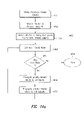
- FIG. 1 a shows a typical design process or “flow” 100 that an integrated circuit designer would use to design a standard cell-based integrated circuit.
- the designer provides a functional or behavioral description of the integrated circuit using a hardware description language.
- the designer specifies timing and other performance constraints ( 109 ) with which the integrated circuit must comply.
- the designer selects a standard cell library to implement the design.
- the standard cells in the library are designed to the requirements of a target manufacturing technology.
- each cell is also characterized to provide performance parametric values such as delay, input capacitance and output drive strength.
- the designer uses a “synthesis tool” to create from the functional or behavioral description a functionally equivalent logic gate-level circuit description known as a “netlist.”
- the elements of the netlist are instances of standard cells selected by the synthesis tool from the standard cell library in accordance with functional requirements and the performance constraints.
- the synthesis tool uses the characteristic parametric values of each standard cell and a model of input and output loads (“wire load model” or “WLM”) to attempt to meet performance requirements.
- WLM wire load model
- a “place and route” tool creates a “physical design” by placing the standard cell instances of the netlist onto the “silicon real estate” and routes conductor traces (“wires”) among these standard cell instances to provide for interconnection.
- the placement and routing of these standard cell instances are guided by cost functions, which minimize wiring lengths and the area requirements of the resulting integrated circuit.
- a more accurate set of parasitic impedance values in the wires can be extracted.
- a more accurate timing analysis can be run at step 106 using a static timing analyzer (STA). If the physical design meets timing constraints, the design process is complete (step 108 ). Otherwise, steps 103 – 106 are repeated after appropriate modifications at step 107 are made to the netlist and the performance constraints.
- STA static timing analyzer
- Design process 100 suffers from a number of disadvantages.
- WLM is a crude model based on statistics. Because of the inaccurate model, a designer typically uses an “80 th percentile WLM” (i.e., 80% of the nets will have a capacitance less than predicted by the WLM). As a result, the drivers for many nets are unnecessarily large, while other driver are too weak. Additionally, designers tend to provide 30% or more additional safety margins to accommodate other inaccuracies in the design flow. Such over-design represents inefficiencies in both silicon area and performance.
- the present invention provides methods and systems for optimizing a post-layout design without requiring re-synthesis.
- accurately extracted timing information from the physical design drives transformation of the physical design, thereby avoiding the inaccuracy of wire load models of the prior art.
- methods and systems of the present invention apply local transformations to the physical design, thereby maintaining substantial integrity (i.e., validity and accuracy) in the interconnect models during the transformation process.
- Accurate models of parasitic impedance can be obtained using an asymptotic waveform evaluation technique.
- one method for post-layout optimization of an integrated circuit includes: (a) providing a logic description of the integrated circuit; (b) synthesizing from the logic description a netlist of the integrated circuit using instances of cells from a standard cell design library; (c) placing and routing the instances to provide a physical design of the integrated circuit; (d) extracting from the physical design models of parasitic impedance of interconnect in the physical design; and (e) optimizing the physical design by modifying the physical design according to the models of parasitic impedance.
- the optimization iteratively (a) identifies, using a static timing analyzer, locations in the physical design where timing violations occur and (b) applies one or more local transformations to the physical design to correct the timing violation.
- the method performs a forward sweep and a backward sweep of the physical design to compute a required signal arrival time and a latest signal arrival time, respectively.
- a library analysis step provides characterization of the standard cell library to allows accurate timing and load driving ability analyses.
- one method enables a cell to be selected from a library to perform a given logic function and to drive a given load capacitance. That method includes: (a) dividing the cells in the library into groups, such that cells within each of the groups perform substantially the same logic function; (b) within each group, assigning to selected cells each an operating range of loads; and (c) selecting a cell by matching the logic function and the given load capacitance to the operating range of the cell.
- the operating range of loads to a cell in the library are assigned according to a metric relating an area of the cell to a delay of the cell.
- each group contains not only cells performing the given function, but also combinations of such cells and buffers of appropriate drive strengths, and combinations of cells providing a complementary logic function and inverters.
- a method of the present invention includes: (a) extracting from the physical design parasitic models of interconnect in the physical design; and (b) applying optimization steps, each optimization step transforming the physical design to achieve a desired performance based on area or delay.
- the optimization steps are applied in order of potential intrusiveness to the physical design.
- the present invention allows the less complex modifications to be accomplished first. Typically, a large portion of the potential optimization can be achieved by these minimally intrusive modifications to the physical design, leaving the physical design to be substantially optimized even before the more intrusive optimization steps are applied.
- an initial optimization step identifies in the physical design a cell instance mismatched to an output load driven by the cell instance; and replaces the cell instance by a second cell instance matched to the output load. Then, a second optimization step computes a potential improvement in slack for each cell instance in the physical design, selects from the physical design cell instances having the largest potential improvements in slack, and applies transformations to the selected cell instances.
- a bidirectional combinational total negative slack (BCTNS) ranking method of the present invention is used.
- the BTCNS ranking method identifies “hot spots” in the physical design, which are locations where performance improvements with the highest potential impact.
- the BTCNS method includes: (a) performing a forward sweep and a backward sweep of the physical design to provide for each cell instance a forward priority value and a backward priority value; (b) calculating an equivalent priority value based on the forward priority value and the backward priority value; and (c) ranking cell instances in the physical design according to the equivalent priority value.
- a third optimization according to a metric based on a path-based algorithm (e.g., a critical path algorithm).
- the path-based optimization can be used to correct hold and set-up time violations.
- the last optimization step identifies in the physical design a cell instance meeting timing requirements but mismatched to an output load driven by the cell instance, and replaces the cell instance by a second cell instance matching the output load and having a smaller silicon area.
- the method of the present invention takes advantage of a static timing analyzer capable of performing incremental timing analysis, and an extraction tool capable of performing incremental extraction of parasitic impedance in the interconnect.
- the local transformations in the present invention include cell instance upsizing, cell instance downsizing, node off-loading, input swapping and logic duplication.
- a system for post-layout design optimization includes: (a) a library interface for access to a standard cell library; (b) a timing analyzer interface for accessing a static timing analyzer; (c) a design tool interface for accessing a place and route design tool; (d) a design database for storing a physical design of an integrated circuit composed of instances of standard cells from the standard cell library.
- the system provides routines for traversing the instances in accordance with predetermined orders, a control program for obtaining timing information of the instances from the static timing analyzer, a control program for applying local transformations of the instances guided by the timing information.
- FIG. 1 a shows a typical design flow 100 that an integrated circuit designer would use to design a standard cell-based integrated circuit.
- FIG. 1 b shows design flow 150 , in accordance with one embodiment of the present invention.
- FIG. 2 shows design flow 200 , representing the operations of step 109 b of FIG. 1 b , in one embodiment of the present invention.
- FIG. 3 is an overview of optimization tool 300 in one embodiment of the present invention.
- FIG. 4 is flow diagram 400 representing library analysis step 201 of FIG. 2 .
- FIG. 5 a shows the drive strengths of cells 501 – 504 .
- FIG. 5 b shows, in the operating range of interest (i.e., 0 to 2 pf), process flow 400 found cells 501 – 503 which cover the entire operating range with their individual operating ranges 0 to C 1 , C 1 to C 2 , and C 2 to 2 pf.
- FIG. 6 shows a network model 600 used in STA 308 .
- FIG. 7 is a flow diagram 700 that illustrates the operations of delay calculator 307 .
- FIG. 8 is a flow diagram 800 showing the operations of Phase 1 optimization, according to one embodiment of the present invention.
- FIG. 9 a is a flow diagram 900 providing an overview of the optimization steps in Phase 2 A.
- FIG. 9 b is a flow diagram 900 providing an overview of the optimization steps in Phase 2 B.
- FIG. 10 is a flow diagram 1000 showing the operations of BCTNS sort step 904 of FIG. 9 a.
- FIG. 11 a shows cell instance 1101 with its output “effective load” modeled by capacitor 1102 (C L ) and input and output signal transition times 1104 , 1105 and 1106 , as computed by delay calculator 307 .
- FIG. 11 b shows assumed operating conditions necessary to achieve a largest possible delay improvement of cell instance 1101 .
- FIG. 12 a is a flow diagram 1250 showing the operations of backward propagation of PV values at step 1008 of FIG. 10 .
- FIG. 12 b shows a backward column PV table initialization step 1200 , used in output pin initialization step 1253 of FIG. 12 a.
- FIG. 12 c shows a flow diagram 1280 that sets forth the steps for backward propagation of values of a PV table to a divergence point.
- FIG. 12 d shows a flow diagram 1260 that illustrates the steps for backward propagation of values of a PV table to a merged point.
- FIG. 13 a shows backward propagation of PV values over a parasitic model that is driven by multiple input terminals.
- FIG. 13 b shows backward propagation of PV values over a cell instance having multiple input terminals.
- FIG. 13 c shows backward propagation of PV values from multiple output terminals of a parasitic model to a single input terminal.
- FIG. 14 a is a flow diagram 1450 showing forward propagation of PV values at step 1009 of FIG. 10 .
- FIG. 14 b shows a forward column PV table initialization step 1400 , used in input pin initialization step 1453 of FIG. 14 a.
- FIG. 14 c shows a flow diagram 1480 that sets forth the operations for forward propagation of values of a PV table to a divergence point.
- FIG. 14 d illustrates forward propagation of PV values to a merge point.
- FIG. 15 a shows forward propagation of PV values over a parasitic model that is driven by multiple input terminals.
- FIG. 15 b shows forward propagation of PV values over a cell instance having multiple input terminals.
- FIG. 15 c shows forward propagation of PV values from a single input terminal of a parasitic model to multiple output terminals.
- FIG. 17 shows flow diagram 1700 , which illustrates the operations for optimization step 908 (i.e., cell downsizing).
- FIG. 18 shows flow diagram 1800 , which illustrates the operations for optimization step 909 (i.e., cell upsizing).
- FIG. 20 is a flow diagram 2000 , which provides an overview of the optimization steps in Phase 3 .
- FIG. 21 shows flow diagram 2100 , which illustrates “input swapping” optimization step 2011 of Phase 3 .
- FIG. 22 shows flow diagram 2200 , which illustrates “logic duplication” optimization step 2012 of Phase 3 .
- FIG. 23 provides an example of circuit optimization by logic duplication.
- FIG. 24 shows flow diagram 2400 , which illustrates a buffer insertion technique for addressing hold time violations.
- FIG. 25 shows flow diagram 2500 , which illustrates a process for matching each output terminal to an optimal driver.
- the present invention provides a design tool and a method for optimizing a standard-cell based integrated circuit after placement and routing are performed, without requiring complete re-synthesis of the integrated circuit design.
- the present invention optimizes the integrated circuit design based on accurate extraction and modeling of the interconnect network.
- FIG. 1 b shows an overview of design flow 150 in one embodiment of the present invention.
- the integrated circuit design steps of synthesis, initial placement and initial routing are not re-iterated. Instead, modifications to the physical design are performed incrementally.
- the timing problems uncovered by timing analysis step 106 b are addressed by an interconnect optimization step 109 b .
- Step 109 b fixes some or all of the timing problems using the local transformation techniques described below.
- step 110 b By providing incremental place and route directives to the corresponding place and route tools.
- step 111 b an incremental extraction of parasitic impedance is performed on the revised physical design.
- Process flow 150 then returns to timing analysis step 106 b to determine if the revised physical design meets all timing requirements. If not, step 109 b , 110 b and 111 b are repeated.
- FIG. 2 shows in further detail step 109 b of FIG. 1 b .
- a standard cell library e.g., a “.lib” file of a format supported by Synopsys Corp.
- cells are classified according to their logic functions (e.g., NAND gates of different drive strengths are grouped), and each cell's operating characteristics (e.g., drive strength at each output terminal and capacitance at each input terminal) are estimated, as explained in further detail below.
- the results are included in an augmented library file (in a suitable format, such as Copernicus Library Format or “CLF”).
- a suitable format such as Copernicus Library Format or “CLF”.
- the design database is prepared for receiving an input netlist.
- the design database provides data structures, described in additional detail below, for facilitating the optimization steps in FIG. 2 .
- the synthesized, placed and routed physical design is then read into the database.
- the design is typically provided, for example, in the LEF and DEF file formats supported by Synopsys, Inc.
- timing and other constraints are also read into the database.
- parasitic impedance models (“parasitic” models) of interconnect wires are incorporated into the database.
- Parasitic models are provided by parasitic extractor 204 , which can be implemented by, for example, the extraction tool “Columbus”, which is available from Frequency Technology, Inc., Santa Clara, Calif.
- the parasitic models are incorporated into the initial netlist.
- Such parasitic models can include such circuit elements as resistors, capacitors and inductors.
- a clock tree analysis is performed by clock tree analyzer 206 to identify clock signals and clock signal paths.
- Clock tree analyzer 206 can be provided internally, or by an external clock tree analyzer (e.g. “Cartier” from Frequency Technology, Inc.) interfaced to the design tool of the present invention.
- the extracted clock information is incorporated into the design database.
- an initial timing analysis is performed.
- the initial timing analysis is performed by a static timing analyzer (STA), which is described in further detail below.
- STA static timing analyzer
- the “slack” of each electrical terminal, or “pin,” is calculated.
- the term “slack” refers to the time difference between the latest signal arrival time and a required signal arrival time.
- a cell instance can also be assigned a slack, which is typically the least slack selected from the cell instance's input and output terminals.
- the design tool of the present invention provides one or more optimization steps. To simplify presentation, only optimization steps 208 and 209 are explicitly shown in FIG. 2 . In one embodiment of the present invention, four optimization steps (identified below as Phases 1 – 4 and described in further detail below) are provided in the design tool.
- the physical design is modified by a number of local transformations—i.e., each transformation affects only a small number of closely related cell instances and nets.
- the local transformations are reported and implemented by providing incremental placement and routing directives to a placement and routing tool (e.g., steps 210 – 212 ).
- a static timing analysis is performed, using the same STA mentioned above. If the timing constraints are met, further optimization is not necessary.
- phase 1 which is a “clean-up” optimization step, the physical design is inspected for load-driver mismatches. A load-driver mismatch occurs when a driver drives a load outside of the driver's optimal range.
- a cell instance can be upsized or down-sized to meet the required timing constraints (i.e., the mismatched cell instance can be replaced by a logically equivalent cell instance with more or less drive strength, or longer or shorter propagation delay).
- Phase 2 In the second phase (“Phase 2 ”), “hot spots” are identified in the physical design.
- a “hot spot” is a cell with a potential timing improvement that can result in a substantial improvement in timing performance both locally and along signal paths that include this cell.
- Phase 2 consists of two phases, referred to below as Phase 2 A and Phase 2 B.
- Phase 2 A is based on a “total negative slack” calculation at each terminal. Negative slack at a terminal is the amount of time by which the expected signal arrival time at the terminal fails to meet the required arrival time, taking into consideration all timing paths leading to the terminal.
- “Total negative slack (or “TNS”)” at a terminal is the cumulative negative slacks over all timing endpoints of interest. An endpoint having a positive slack is ignored. More detailed information regarding TNS can be obtained, for example, from Synopsis, Inc. Depending on the nature of the hot spot, one or more local transformations can be applied to realize the timing improvements.
- Phase 3 a third phase also applies local transformations to correct “setup” timing violation in signal paths.
- Phase 4 A “hold” timing violations in signal propagation paths are corrected.
- a “hold” time violation occurs when a signal transition at a clocked element (i.e., a sequential element, such as a flip-flop) occurs prior to the previous logic value of the signal is latched by the clocked element.
- a “setup” timing violation occurs when the clocked element latches a signal prior to the signal's arrival.
- Phase 4 B the physical design is examined to clean up of any remaining mismatch between operating point of the cell instances and the driven load, by downsizing appropriate cell instances.
- a more aggressive design style can be used. For example, a 50% WLM target can be set in the synthesis step, so as to leave a larger portion of the timing violations to be corrected by the optimization steps. Under such an arrangement, over-design in the final physical design is reduced, resulting in a lower silicon area and a more timing-efficient integrated circuit. Because the present invention applies local transformations, rather than relying on a global re-synthesis, changes to the placed and routed physical design are incremental and minimally intrusive. Physical design optimization can therefore be achieved much more quickly than in the prior art.
- FIG. 3 is an overview of optimization tool 300 in one embodiment of the present invention.
- Design tool 300 includes an overall control program 301 , which controls and sequences the process flow 200 in FIG. 2 , for example.
- design database (“design graph”) 305 contains the data structures representing the physical design at all times. Some examples of objects in design graph 305 includes:
- Interfaces 310 – 313 To import the placed and routed physical design and the timing and performance constraints, interfaces 310 – 313 are provided. Interfaces 310 – 313 each translate design data or constraints expressed in an industry standard data format to internal data structure of design graph 305 .
- the physical design can be exported to an external tool to perform further design activities, such as to perform incremental placement and routing, or to perform more accurate extraction of parasitic impedance.
- Interface 304 translates selected data structures of design graph 305 into industry standard formats accepted by the external tool.
- Algorithms 315 include routines for traversing design graph 305 , thus allowing application programs in optimization tool 300 to extract information in design graph 305 in specified orders. Some examples of such routines include routines for returning a cluster, a cell, a net or a path in depth-first, breadth-first or another ranked order. (A cluster is a group of combinational logic elements between two clocked elements in common or related clock domains.) Specifically, algorithms 315 provide routines for a “forward sweep” and a “backward sweep” of a cluster. These operations are explained in further detail below. Algorithms 315 provide an internal interface between functional modules (e.g., transformation routines 309 , described below) and design graph 305 .
- functional modules e.g., transformation routines 309 , described below
- FIG. 3 shows four functional modules: optimization module 302 , transform module 309 , STA 308 and delay calculator 307 .
- Delay calculator 307 which is described in further detail below, computes a delay in a given net using an “asymptotic waveform evaluation” (AWE) method.
- STA 308 performs both the initial static timing analysis (e.g., step 207 of FIG. 2 ) and the static timing analysis after each optimization step (e.g., steps 208 – 209 ), as mentioned above.
- Transformation module 309 includes all programs for transforming a Node. During an optimization step, transformation module 309 invokes STA 308 to evaluate each applicable transformation.
- Optimization module 302 includes all programs for executing the optimization steps (e.g. Phases 1 – 5 ). Optimization module 302 invokes transformation module 309 to implement local transformations.
- FIG. 4 is a flow diagram 400 representing library analysis step 201 of FIG. 2 in one embodiment.
- a user provides a desired relative “delay to area” tradeoff ratio (“ ⁇ desired ”) 402 , the basic driver 403 of the given technology (typically, a small buffer cell in the library), a “load increment” ⁇ C L value 404 (i.e., the finest load capacitance resolution for the library analysis), and the standard cell library file (.LIB) 405 , including all performance characterization data.
- ⁇ desired relative “delay to area” tradeoff ratio
- ⁇ desired the basic driver 403 of the given technology
- ⁇ C L value 404 i.e., the finest load capacitance resolution for the library analysis
- .LIB standard cell library file
- a relative “delay to area” tradeoff ratio (denoted ⁇ i,j,k ) is used to control cell selection.
- ⁇ i,j,k is a measure of the delay advantage gained by replacing cell i by cell j under the condition of an output load k.
- ⁇ i,j,k results in a design optimized towards higher speed performance.
- ⁇ i,j,k results in a design optimized towards reducing silicon area.
- the standard cells are grouped according to logic functions (e.g., NAND, OR, NOR, AND, XOR, etc.).
- Standard cells included in the same logic function group are interchangeable with respect to logic function. Two cells belong to the same function group if they have the same number of input and output terminals or “pins”, perform the same logic function and provide, at each output pin, the same output “sense”—i.e., negative or positive logic.
- groups that perform “complementary” logic functions e.g., AND and NAND
- Standard cells in complementary logic function groups are interchangeable by the insertion of an inverter. Step 401 further identifies:
- library analysis step 201 examines all function groups individually (i.e., step 406 of FIG. 4 ). For each function group (selected at step 408 ), a zero-load cell delay is calculated for each standard cell within the function group (step 409 ).
- the delay for a standard cell i driving an output load C L is denoted by D(i, C L ).
- the zero-load cell delay for cell i is denoted D(i, 0 ).
- the zero-load cell delay D(i, 0 ) of a given standard cell i can be obtained, for example, using delay calculator 307 of FIG. 3 by evaluating the standard cell's delay response when driven by basic driver 403 with an ideal rising or falling transition. In one embodiment, the standard cell's delay responses are estimated for both rising and falling transitions. Delay calculator 307 is discussed in further detail below.
- the mean value D m (0) of all zero-load delays in a function group and the mean area A m of all cells in that function group are computed.
- the cells in the function group are sorted according to their drive strengths (e.g., in order of increasing area).
- the next steps i.e., steps 412 – 421 ) find the operating ranges of the cells in the function group.
- the operating range of each cell is defined between a “low load” operating point (C LL ) and a “high load” operating point (C HL ).
- ⁇ i , j , k D ⁇ ( i , k ) - D ⁇ ( j , k ) D m ⁇ ( 0 ) A ⁇ ( j ) - A ⁇ ( i ) A m in which, D(i,k) and D(j,k) are respectively the delays of cells i and j under a load k, D m (0) is the mean value of all zero-load delays for cells in logic function group, A(i) and A(j) are the areas of cells i and j, and A m is the mean area of all cells in the function group, as mentioned above.
- the current C HL is the “high load” operating point for cell i (step 418 ).
- Cell j which has the largest ⁇ i,j,k that exceeds ⁇ desired , is selected (step 419 ) as the cell to operate in the next operating range, with a C LL value assigned the current C HL value (step 420 ), and an initial C HL equaling the current C HL plus ⁇ C L (step 414 ).
- the next function group is selected (step 406 ) after all the cells in the present function group providing coverage for the operating ranges of interest are identified (as determined by step 421 ).
- Library analysis step 201 completes after all function groups are processed (step 407 ).
- FIGS. 5 a and 5 b illustrate the results of applying process flow 400 to compute the operating ranges for standard cells in a NAND group.
- FIG. 5 a shows the drive strengths of standard cells 501 – 504 .
- the operating range of interest zero to 2 pf, are found covered by standard cells 501 – 503 , with operating ranges (0, C 1 ), (C 1 ,C 2 ), and (C 2 , 2) pf.
- timing analysis is provided by STA 308 of FIG. 3 .
- STA 308 can be called upon to compute path delays in circuits that can include state elements and combinational logic elements.
- cell instances in the design database that are inserted or modified since the last timing analysis are marked.
- Incremental timing analysis is achieved by computing timing for these marked instances and instances whose timing is affected by such marked instances. Suitable techniques for providing this incremental timing analysis capability can be found, for example, in “An Algorithm for Incremental Timing Analysis,” by Lee et al., published in The Proceedings of the 32 nd ACM/IEEE Design Automation Conference (1995).
- FIG. 6 shows a network model 600 used in STA module 308 .
- the signal arrival time at input terminal 602 is provided by an “entry delay” relative to a clock signal 606 , based on an assumption that the input signal is driven by an output driver of an upstream state element 604 .
- the required signal arrival time at output terminal 603 is provided by an “exit delay”, relative to clock signal 612 , based on an assumption that the output signal is fed into an input terminal of second state element 605 .
- Entry and exit delays are computed from clock terminals identified by a clock analysis step, such as clock analysis step 206 of FIG. 2 . To accommodate interacting clocks, clock skews and offset between clocks are modeled in STA 308 .
- STA module 308 can use a primary input terminal, a clock terminal in a state element, or a terminal with user-specified constraints as a start timing point. Similarly, STA 308 can use a primary output terminal, a terminal with a defined setup time or a terminal with user-specified constraints as a timing end point.
- Circuit 601 includes clusters 607 and 610 , which are each a combinational circuit that couples an output terminal of a first state element and an input terminal of a second state element.
- Cluster 607 is a combinational circuit between flip-flops 604 and 608
- cluster 610 is a combinational circuit between flip-flops 608 and 609 .
- Timing within a cluster is calculated “stage” by “stage” using, for example, delay calculator 307 , which is mentioned above.
- a stage begins at the input terminals of a driver cell instance providing output signals, and ends at the input terminals of receiver cell instances receiving the driver cell instance's output signals.
- delay calculator 307 commercial timing calculators, such as “PrimeTime”, from Synopsys Corporation, or the “Central Delay Calculator”, from Cadence Design Systems can also be used.
- STA 308 To allow signal timing through a stage to be calculated, STA 308 requires (a) pin-to-pin cell delays from the cell library, which can be estimated, for example, in library analysis step 201 of FIG. 2 , as mentioned above, and (b) interconnect parasitic models, which can be extracted, for example, by parasitic extraction step 204 of FIG. 2 , as mentioned above. STA 308 also accepts from a user a list of false paths, which guides the timing analysis and allows more accurate results. STA 308 computes (a) for each input and output terminal, a “worst” slack value, (b) for each cell instance, a cell delay, and (c) at each output terminal of a cell instance, an “effective load” model.
- STA 308 performs a “forward sweep” and a “backward sweep.”
- STA 308 starts from the start timing points and traverses cell instances and parasitic models level by level (i.e., using the well-known critical path method, or “CPM”) to compute a “latest arrival time” (LAT) at each terminal.
- LAT is the longest cumulative delay to the current pin relative to a timing start point. (The LAT at a timing start point is the “entry delay.”)
- the timing of a cell instance or parasitic model is computed only after the timing for all cell instances driving the input terminals of the cell instance or parasitic model are computed.
- the timing data associated with a forward sweep are: (a) the LAT at each input terminal; (b) the input transition time used to compute the delay at each input terminal; and (c) pin-to-pin delay between any input terminal of the cell instance or parasitic model to any output terminal of the cell instance or parasitic model.
- RAT is the longest cumulative delay from the current pin relative to a timing end point. (RAT at a timing end point is the “exit delay.”)
- the RAT is computed only after computing RATs for all cell instances connected to the output terminals of the cell instance.
- a “slack” value for the terminal is computed.
- the slack is negative, i.e., the expected latest arrival time is later than the required arrival time, a timing violation is detected.
- the smallest slack among the multiple slacks (which may be negative) is selected as the “cell slack”.
- delay calculator 307 uses a graph of the stage, parasitic models representing the interconnect wires between the output terminals of the driver cell instance and the input terminals of the receiver cell instances, and input time transitions at all input terminals of the driver cell instance.
- Delay calculator 307 outputs delay and transition times for both positive- and negative-going transitions at each output terminal of the driver cell instance and at each input terminal of the receiver cell instances.
- an effective load model is provided to each output terminal of a cell instance.
- FIG. 7 is a flow diagram 700 that illustrates the operations of delay calculator 307 .
- a capacitance is obtained from the cell library to represent the capacitance load at the input terminal of the receiver cell instance.
- the parasitic model of the interconnect wires between the output terminal of the driver cell instance and an input terminal of a receiver cell instances is combined with the input capacitances at the receiver cell instances to create a reduced-order model.
- a ⁇ -model is provided using the first three moments of the driving point admittance.
- a suitable method for creating a ⁇ -model from the first three moments is described, for example, in “An explicit rc-circuit delay approximation based on the first three moments of the impulse response,” by Tutuianu et al., IEEE Design Automation Conference, 1996. Higher accuracy can be achieved using higher order models.
- the size of the “effective load” capacitor C eff is iteratively derived by equating the average current from the reduced-order model with the single capacitor model. Also, during this step, using the input transition time (“slew rate”) at each input terminal of the driver cell, a gate delay t gate and an output transition time or slew rate at an output terminal of the driver cell instance are computed.
- step 704 using the reduced-order model of step 702 , and the output transition times computed at step 703 , the input transition time at each input terminal of the receiver cell instances is calculated.
- the input transition times are obtained using a Newton-Raphson iteration scheme on the ⁇ -model mentioned above.
- step 805 if the cell slack is determined to be non-negative, i.e., no timing violation has occurred at that cell, the cell is skipped over. However, if the cell slack is determined to be less than zero, the effective load C eff of the cell instance is then examined to determine if C eff is within the operating range of the cell instance. If C eff is within the operating range of the cell instance, nothing further is done for that cell instance.
- one of the following local transformations is invoked at step 807 : (i) replacing the current cell instance by a larger cell instance in the same function group with an operating range covering C eff ; (ii) inserting a buffer that has an operative range covering C eff , or (iii) replacing the current cell instance by a combination of an instance of a cell in the complementary function group and an inverter with a drive covering C eff .
- timing is recomputed at step 820 .
- a second “backward sweep” is set up at step 810 . Again, each cell instance encountered during the backward sweep is examined (step 811 ). At step 813 , if the cell slack is determined to be negative, i.e., a timing requirement violation has occurred, the cell instance is skipped over. Skipping over this cell instance avoids creating a timing violation as a result of a downsizing step or a buffer elimination step. Downsizing and buffer elimination are local transformations that can be applied at this second backward sweep.
- the effective load C eff of the cell is examined to determine if C eff is within the operating range of the cell instance. If C eff is within the operating range of the cell instance, nothing further is done for that cell instance.
- one of the following transformations is invoked at step 815 : (i) replacing the current cell instance by a smaller cell instance in the same function group with an operating range covering C eff ; or (ii) removing a buffer, so as to allow the weaker drive strength of the cell instance to directly drive C eff , or (iii) replacing the current cell instance by a combination of a cell instance in the complementary function group and an inverter with a drive operating range covering C eff .
- FIG. 9 a is a flow diagram 900 showing an overview of the optimization steps in Phase 2 A.
- the physical design is first partitioned into clusters at step 901 .
- a netlist that has its logic circuits partitioned into clusters is referred to as a “cluster-partitioned netlist”.
- Optimization under the BCTNS algorithm proceeds on a cluster by cluster basis (i.e., repeating steps 902 – 910 ), until all clusters are optimized (step 912 ).
- the cells within the cluster are first ranked by BCTNS sorting step 904 in descending order of worst BCTNS values.
- a user-specified number of cells are then selected one by one in the sorted order (steps 905 and 906 ) for optimization.
- BCTNS values are recomputed after each optimization pass.
- BCTNS sorting step 904 is illustrated by flow diagram 1000 of FIG. 10 .
- STA 308 annotates slack values on the physical design.
- the BCTNS algorithm computes a “potential improvement” (PI) value for each cell in a given cluster.
- PI is computed according to the circuit models shown in FIGS. 11 a and 11 b .
- FIG. 11 a shows cell instance 1101 with its output “effective load” modelled by capacitor 1102 (C L ) and input and output signal transition times 1104 , 1105 and 1106 , as computed by delay calculator 307 in the manner described above.
- delay calculator 307 the delay between an input terminal of cell instance 1101 and output terminal 1105 is denoted D current .
- FIG. 11 b shows the assumed operating conditions necessary to achieve PI.
- cell instance 1101 is replaced by cell instance 1151 , which is the largest driver in cell instance 1101 's function group with each input terminal driven by basic drivers with an ideal step waveform.
- Delay calculator 307 then computes the delay D best under the conditions of FIG. 11 b .
- PI is defined as the difference between D current and D best .
- the largest PI (PI max ) and the least PI (PI min ) obtained for the cluster are identified (step 1005 ).
- a data structure is created to represent a three-column table (“Priority Value” or PV table) having a user-specified number T s of rows (step 1013 ).
- the value r* ⁇ PI where ⁇ PI is (PI max ⁇ PI min )/T s , fills column 1 of each row r of the PV table, denoted by “PV(r, 1 )” (step 1007 ).
- PV(r, 1 ) fills column 1 of each row r of the PV table
- column 2 (“PV(r, 2 )”) of each PV table in the cluster is filled by backward propagation of PV values from the output terminals of the cluster.
- column 3 (“PV(r, 3 )”) of each PV table in the cluster is filled by forward propagation of PV values from input terminals of the cluster.
- an “equivalent priority value” (“EPV”) is computed for each cell according to flow diagram 1600 of FIG. 16 .
- BCTNS sort step 904 for the cluster is complete after the cells in the cluster are ranked in decreasing EPV order.
- backward propagation of PV values step 1008 of FIG. 10 is illustrated by flow diagram 1250 of FIG. 12 a .
- backward propagation of PV values begins from a timing-annotated cluster (step 1251 ).
- Algorithms 315 routines for traversing the cell instances of the cluster are initialized at step 1252 .
- a backward column initialization step 1253 fills column 2 of the PV table for each output terminal of the cluster, as discussed below in conjunction with FIG. 12 b .
- steps 1254 – 1257 a backward sweep traces from the output terminals of the cluster stage by stage back to the input terminals of the cluster.
- the backward sweep first propagates PV values at the output terminals of the parasitic interconnect model to the input terminal or terminals of the parasitic model (step 1256 ), and then continues to propagate the PV values at these input terminals of the parasitic interconnect model over the cell instance to the input terminals of the cell instance (step 1257 ).
- the nets of the input terminals of the stage are taken as the output terminals of the stage become “ready”.
- a net is said to be “ready” in this context after the values in the second column (i.e., PV(r, 2 )) of its PV table are filled. Backward propagation of PV values is complete when all ready nets are traversed.
- Flow diagram 1200 of FIG. 12 b illustrates backward column initialization step 1253 .
- initialization step 1253 begins at step 1201 with a timing-annotated cluster, as discussed above.
- steps 1202 – 1211 fill column 2 of the PV table of every output terminal (i.e., the timing end points) of the cluster.
- the slack S for the output terminal is added to potential improvement value PV(r, 1 ) in the first column of the same row r (step 1206 ) to provide an improved slack value S′ for that output terminal.
- improved slack value S′ is greater than 0 (i.e., timing is met by this improvement)
- the backward PV value of row r i.e., PV(r, 2 )
- the incremental improvement value for the corresponding PI value of column 1 of the PV table i.e., ⁇ S*PV(r, 1 )
- PV values are propagated at steps 1256 and 1257 by a backward sweep over parasitic interconnect models and over cell instances, respectively.
- a parasitic model is driven by multiple input terminals, as illustrated by FIG. 13 a , or is driven by an output terminal of a cell instance having multiple input terminals, as illustrate by FIG. 13 b
- the values in the PV table of the output terminal are propagated to divergence points.
- the values of the PV table of output terminal 1301 are propagated backwards to the PV tables of input terminals 1302 and 1303 .
- FIG. 13 a the values of the PV table of output terminal 1301 are propagated backwards to the PV tables of input terminals 1302 and 1303 .
- the values in the PV table of output terminal 1304 of cell 1307 are backward propagated to the PV tables of input terminals 1305 and 1306 of cell instance 1307 .
- the values of the PV table of output terminals of the parasitic interconnect model e.g., output terminals 1321 , 1322 and 1323
- the values of the PV table of output terminals of the parasitic interconnect model are propagated to a merge point at terminal 1324 .
- different procedures are provided for backward propagation of the values of a PV table for propagating to divergence and merge points, as illustrated by the flow diagrams in FIGS. 12 c and 12 d , respectively.
- FIG. 12 c shows a flow diagram 1280 that illustrates the steps for backward propagation of values of a PV table to a divergence point.
- a running index i is initialized to zero.
- Index i indicates the current input terminal of the parasitic model or the cell instance (“parent”) whose column 2 of the PV table is to be filled. For example, if the parasitic model has three input terminals, then index i runs from 0 to 2.
- Steps 1282 , 1283 and 1284 step through each input terminal of a parasitic model or a cell instance to fill in the rows of the PV table of the input terminal one by one.
- Index k which is initialized at step 1285 , is another running index for traversing the same input terminals of the cell instance or parasitic model.
- PV(row, 2 ) i.e., the current row in the PV table of the current input terminal
- the slack s(k) of input terminal k and PV(row, 1 ) of output terminal k times PI are summed to provide an improved slack s′ (k) (step 1287 ).
- the improved slack s′ (k) exceeds 0, the improved slack s′ (k) is set to 0 (steps 1288 and 1289 ).
- PV(row, 2 ) of input terminal i provided the ratio of its slack improvement to the total slack improvement r (i.e., (s′(i) ⁇ s(i))/r).
- PV(row, 2 ) represents a measure of the relative contribution of slack improvement among the input terminals, given the propagated PV(row, 2 ) of the output terminal.
- FIG. 12 d shows a flow diagram 1260 that illustrates the steps for backward propagation of values of a PV table to a merged point.
- entry PV(i, 2 ) is assigned the sum of all corresponding PV(i, 2 ) in the PV tables of the output terminals (“children”) of the cell instance or parasitic model, as steps 1263 , 1265 and 1266 iterate over all rows of the PV table of the input terminal of the cell instance or parasitic model.
- flow diagram 1450 of FIG. 14 a Forward propagation of PV values step 1009 of FIG. 10 is illustrated by flow diagram 1450 of FIG. 14 a .
- flow diagram 1450 of FIG. 14 a is substantially identical to flow diagram 1250 of FIG. 12 a .
- a detailed description of flow diagram 1450 is omitted.
- the descriptions of the following flow diagrams are also omitted: (a) flow diagram 1400 of FIG. 14 b , which illustrates forward column initialization step 1453 of FIG. 14 a ; (b) flow diagram 1460 of FIG. 14 c , which illustrates forward propagation of PV values to a divergence point; and (c) flow diagram 1460 of FIG. 14 d , which illustrates forward propagation of PV values to a merge point.
- FIGS. 15 a , 15 b and 15 c illustrate, respectively, forward propagation (a) when a parasitic model is driven by multiple input terminals, (b) when an output terminal of a cell instance has multiple input terminals, and (c) from multiple input terminals of a parasitic model to a single output terminal (“merge point”).
- FIG. 16 shows flow diagram 1600 that illustrates the steps for computing EPV for each cell in the cluster.
- the PI of a cell instance C is identified.
- the value PI is used to identify two rows containing the closest values to PI.
- a backward PV (“BPV”) value is then obtained by interpolation between corresponding PV values in column 2 of the PV table of the output terminal.
- a forward PV (“FPV”) value is obtained by interpolation between PV values in column 3 of the PV table.
- the cell instances of the cluster are ranked in decreasing EPV order, as discussed above, at step 1011 of FIG. 10 .
- FIG. 17 shows flow diagram 1700 , which illustrates the steps for optimization step 907 (i.e., cell downsizing).
- the cell instances (“children”) driven by a driver cell instance A are examined one by one.
- Slacks SA and S denote the slacks at output terminals of driver cell instance A and at child instance i, respectively (steps 1703 , and 1714 ).
- the running index i keeps track of which of children cell instances is being examined. If the slack S of child cell instance i (i.e., the slack on the output terminal of child cell instance i) is less than a predetermined threshold value S m (step 1704 ), no further action on child cell i is performed. The running index i is incremented at step 1712 to select the next child cell instance. Otherwise, slack S of child cell instance i is greater than threshold value S m , the operating range of child cell instance i is checked (step 1705 ).
- cell instance i is replaced by an instance of a cell C opt of the function group of cell instance i (step 1715 ). Otherwise, i.e., if the load driven by cell instance i is not within cell instance i's operating range, no further action is taken with respect to cell instance i.
- the running index i is incremented at step 1712 to select the next child cell instance.
- STA 308 is called at step 1707 to re-compute timing in the local cluster.
- the recomputed slacks SA′ and S′ of driver cell instance A and replaced cell instance i are calculated at steps 1708 and 1716 , respectively.
- FIG. 18 shows flow diagram 1800 , which illustrates the operation of optimization step 908 (i.e., cell upsizing).
- the cell library is searched to determine whether there exists (i) an optimal cell C o in the same function group as cell instance C with an operating range encompassing load L, and (ii) a combination C c within the same function group as cell instance C and buffer having an operating range encompassing load L (steps 1808 – 1809 ). If neither optimal cell C o nor combination C c exists, no transformation is available (step 1826 ). Otherwise, if only one local transformation is available (i.e., if either optimal C o or combination C c exists, but not both exist), the local transformation is applied (steps 1822 and 1823 ).
- steps 1801 – 1807 first examine every cell instance (“parent cell instance”) C p that drives an input terminal of cell instance C.
- Running index i which is initialized at step 1801 , indicates which parent cell instance is currently under consideration.
- the load L i driven by each parent cell instance C p is examined to determine if load L i is within the optimal operating range of parent cell instance C p (steps 1803 – 1806 ). If the load is not within the optimal operating range of parent cell instance C p , an optimal cell C o ′ is identified and substitutes for cell instance C p . The process returns to step 1802 until all parent cell instances are examined.
- step 1812 the following quantities are computed: (i) the sum S o of worst negative slack WNS 1 at the input terminals of cell instance C and “delta” slack S 1 (i.e., the slack between the input terminal of cell instance C having the worst negative slack and the output terminal of cell instance C), on the basis of an instance of cell C o substituting for cell instance C; (ii) the sum S c of worst negative slack WNS 2 and delta slack S 2 , on the basis of an instance of C c substituting for cell instance C; and (iii) the difference ⁇ S between S o and S c .
- S o represents the slack at the output terminal of cell instance C o , if cell C o substitutes in cell instance C.
- S c represents the slack at the output terminal of the instance of combination C c , if that instance of combination C c substitutes for cell instance C.
- the selected transformation is applied at step 1816 .
- the transformations made to parent nodes i.e., step 1806 ) are then reversed at step 1819 .
- FIG. 19 shows flow diagram 1900 , which illustrate the operations for optimization step 910 (i.e., node off-loading).
- Flow diagram 1900 provides for node off-loading of a cell instance C driving multiple input terminals as an output load.
- steps 1902 – 1904 the slack S c of the output terminal of cell instance C, the topology of the net N driven by the output terminal, and the branches B on net N (i.e., the parasitic models between the output terminal of cell instance C and the input terminals of children cell instances) are obtained.
- the impedance L i of each branch of net N is computed and the resulting impedances are ranked in decreasing order of load.
- step 1921 If slack improvement AS does not exceed a predetermined threshold S min , no further processing is needed (step 1921 ). Otherwise, at step 1919 , BUF is inserted into branch B i and local timing at cell instance C is recomputed after the buffer insertion. The process then returns to step 1903 , after an incremental timing analysis on cell instance is performed by STA 308 to determine if further optimization of net N is possible.
- STA 308 performs a static timing analysis to determine the effectiveness of the optimization steps. If timing is improved by a predetermined threshold amount, at step 911 , the BCTNS algorithm of step 904 is re-run to rerank the cells in the cluster. Otherwise, i.e., timing improvement does not exceed the predetermined threshold amount, no further optimization is attempted on the present cluster. The next cluster is then selected upon return to step 903 .
- Phase 2 B optimization steps can be run.
- Phase 2 B is illustrated by flow diagram 950 of FIG. 9 b .
- optimization is performed on a timing-annotated netlist partitioned into clusters (step 951 ).
- processing is carried out cluster by cluster (steps 952 , 953 , 961 ).
- a backward sweep traverses the cluster Node by Node (steps 954 – 956 ).
- a Node is a macro in the physical design).
- Steps 957 , 958 and 959 are respectively substantially identical to the downsizing step 907 , upsizing step 908 and node off-loading step 909 discussed above.
- timing in the cluster is recomputed (step 960 ). The process then returns to step 952 for operation on the next cluster, until all clusters are processed (step 961 ).
- Phase 3 is illustrated by flow diagram 2000 of FIG. 20 .
- optimization is performed on a timing-annotated netlist partitioned into clusters ( 2001 ). Processing is carried out cluster by cluster (steps 2002 – 2003 ). In each cluster, at step 2004 , STA 308 is called to identify a path with the worst negative slack (steps 2005 – 2007 ). For each Node, optimization steps 2008 – 2012 are carried out. Optimization steps 2008 – 2010 are respectively substantially identical to the downsizing step 907 , upsizing step 908 and node off-loading step 909 discussed above. Optimization steps 2011 and 2012 , corresponding to optimization involving “input swapping” and “logic duplication” are discussed in further detail below.
- step 2014 timing in the cluster is recomputed (step 2014 ), if a Node is optimized during the traversal of the path.
- the process returns to step 2004 to identify a path in the cluster having the worst negative slack. However, if no node is optimized during the last iteration within the cluster, the process returns to step 2002 for operation on the next cluster, until all clusters are processed (step 2015 ).
- FIG. 21 shows flow diagram 2100 which illustrates “input swapping” optimization step 2011 .
- Input swapping optimization step 2011 examines cell instances or Nodes whose slack performance can be improved by swapping input terminals.
- the slack S c of Node C's output terminal is obtained (step 2102 ).
- An input terminal I target of the Node C is identified on a path that is being considered for optimization.
- intrinsic input-to-output delay D i between each input terminal of Node C and the output terminal of Node C is obtained (step 2105 ).
- D min is compare to the intrinsic delay D target between input terminal I target and the output terminal of Node C. If D min substantially equals or exceeds D target , no optimization can proceed, since swapping I min with I target does not result in a significant improvement (step 2119 ).
- the local timing on Node C, children of Node C, and other cell instances also receiving signals from input terminals I target and I min are recomputed, assuming input terminals I target and I min are swapped (steps 2110 and 2111 ).
- slack S c ′ at the output terminal of Node C is recomputed.
- FIG. 22 shows flow diagram 2200 that illustrates “logic duplication” optimization step 2012 of Phase 3 .
- FIG. 23 provides an example of an optimizing step using logic duplication.
- cell instance 2301 drives input terminals of cell instances 2302 – 2307 .
- Logic duplication is applied to logic circuit 2300 to provide logic circuit 2350 .
- an additional cell instance 2308 which is identical to cell instance 2301 , is provided.
- Cell instance 2308 is driven by the same input signals as cell instance 2301 .
- Cell instance 2308 drives cell instance 2307 , which is severed from the output terminal of cell instance 2301 . If cell instance 2307 is a cell in a critical path, by duplicating cell instance 2301 in cell instance 2308 and appropriately sizing cell instance 2308 , the signal delay in the critical path can be reduced.
- the slack S c at the output terminal of cell instance C and the parasitic network representing the net N at the output terminal of cell instance C are obtained (steps 2202 – 2204 ).
- a critical path Node N c can be identified.
- a circuit topology can be created in which Node N c is severed from net N.
- a new cell instance C′, which is an instance in cell instance C's function group is then provided in this new circuit topology to drive N c (steps 2207 – 2208 ).
- step 2210 local timing is then computed for this new circuit topology, which includes cell instances C and C′, their “children” cell instances, and “sibling cell instances” (i.e., cell instances sharing common input terminals with cell instances C and C′.
- the slack S c ′ at the output terminal of cell C′ is calculated (step 2211 ).
- FIG. 24 shows flow diagram 2400 , which illustrates a buffer insertion technique for addressing hold time violations.
- Hold time violations usually result from clock skews or phase differences between common or related clocks.
- a new signal transition may arrive at a state element before the previous signal can be latched.
- the process of flow diagram 2400 inserts one or more buffers to lengthen the signal path.
- the process of flow diagram 2400 begins at step 2401 with a timing-annotated netlist that is cluster partitioned. The clusters in the netlist are examined one by one.
- STA 308 is called to identify one by one signal paths with a hold time violation (steps 2402 – 2404 ).
- the amount H indicating the extent of the hold time violation is calculated (step 2406 ).
- an equivalent number N of basic driver delays is calculated (step 2407 ).
- a basic driver delay is the delay of the smallest driver in the cell library.
- the end point P t of the signal path having the hold time violation is then identified (step 2408 ).
- P t is an input terminal to a state element.
- N serially connected basic buffers are then inserted between P t and the input terminal of the state element at the end of the signal path. Timing is then recomputed for the cluster (step 2411 ).
- the process then returns to step 2404 to process the next signal path with a hold time violation.
- Phase 4 A completes when all paths with hold time violations in all clusters are processed.
- each cell instance is examined to ensure that a minimal driver is provided at each output terminal.
- a process for implementing Phase 4 B is illustrated in FIG. 25 by flow diagram 2500 .
- the process of flow diagram 2500 begins at step 2501 with a timing annotated netlist that is partitioned into clusters.
- the process of flow diagram 2500 traverses the netlist cluster by cluster and, within each cluster computes PI for each cell instance, traversing from the output terminals of the cluster (steps 2503 – 2505 .
- Each Node with a positive slack is examine to determine if the output load is within the optimal operating range of the Node, by identifying the cell N o whose optimal operating range encompasses the output load (step 2506 – 2508 ).
- step 2509 If the current Node is not optimal, the current Node is replaced by an instance of N o (step 2509 ). The process then returns to step 2504 for the next Node, until all Nodes in the cluster are traversed. Timing for the cluster is recomputed after traversal of all Nodes in a cluster (step 2510 ). Phase 4 B completes after all clusters in the netlist are traversed (step 2512 ).
Abstract
Description
-
- a. “Macro”—a representation of a standard cell in the standard cell library;
- b. “MacroPin”—a terminal of a Macro;
- c. “Timing Arc”—a data structure representing the propagation delay between two MacroPins;
- d. “Node”—an instance of a Macro;
- e. “NodePin”—a terminal in a Node;
- f. “Net”—a net connecting two or more NodePins;
- g. “TransformFactory”—a data structure representing a collection of transformation applicable to a Node; and
- h. “Transform”—an instance of a transformation in a TransformFactory.
-
- (a) buffers, inverters, and primary input and output cells (i.e., registers, flip-flops and other state elements) in the cell library;
- (b) for each state element, clock signal terminals and the timing requirement between the clock terminal and each input or output terminal of the state element;
- (c) for each cell, the area of the cell, the drive strength—i.e., delay as a function of load—of each output terminal and the loading of each input terminal; and
- (d) for each combinational logic cell, a propagation delay.
in which, D(i,k) and D(j,k) are respectively the delays of cells i and j under a load k, Dm (0) is the mean value of all zero-load delays for cells in logic function group, A(i) and A(j) are the areas of cells i and j, and Am is the mean area of all cells in the function group, as mentioned above.
Claims (16)
Priority Applications (1)
| Application Number | Priority Date | Filing Date | Title |
|---|---|---|---|
| US10/387,644 US7222311B2 (en) | 2000-03-01 | 2003-03-12 | Method and apparatus for interconnect-driven optimization of integrated circuit design |
Applications Claiming Priority (2)
| Application Number | Priority Date | Filing Date | Title |
|---|---|---|---|
| US09/516,489 US6591407B1 (en) | 2000-03-01 | 2000-03-01 | Method and apparatus for interconnect-driven optimization of integrated circuit design |
| US10/387,644 US7222311B2 (en) | 2000-03-01 | 2003-03-12 | Method and apparatus for interconnect-driven optimization of integrated circuit design |
Related Parent Applications (1)
| Application Number | Title | Priority Date | Filing Date |
|---|---|---|---|
| US09/516,489 Division US6591407B1 (en) | 2000-03-01 | 2000-03-01 | Method and apparatus for interconnect-driven optimization of integrated circuit design |
Publications (2)
| Publication Number | Publication Date |
|---|---|
| US20030177455A1 US20030177455A1 (en) | 2003-09-18 |
| US7222311B2 true US7222311B2 (en) | 2007-05-22 |
Family
ID=24055819
Family Applications (2)
| Application Number | Title | Priority Date | Filing Date |
|---|---|---|---|
| US09/516,489 Expired - Lifetime US6591407B1 (en) | 2000-03-01 | 2000-03-01 | Method and apparatus for interconnect-driven optimization of integrated circuit design |
| US10/387,644 Expired - Lifetime US7222311B2 (en) | 2000-03-01 | 2003-03-12 | Method and apparatus for interconnect-driven optimization of integrated circuit design |
Family Applications Before (1)
| Application Number | Title | Priority Date | Filing Date |
|---|---|---|---|
| US09/516,489 Expired - Lifetime US6591407B1 (en) | 2000-03-01 | 2000-03-01 | Method and apparatus for interconnect-driven optimization of integrated circuit design |
Country Status (1)
| Country | Link |
|---|---|
| US (2) | US6591407B1 (en) |
Cited By (20)
| Publication number | Priority date | Publication date | Assignee | Title |
|---|---|---|---|---|
| US20060248486A1 (en) * | 2005-03-11 | 2006-11-02 | Stmicroelectronics Limited | Manufacturing a clock distribution network in an integrated circuit |
| US20070006106A1 (en) * | 2005-06-30 | 2007-01-04 | Texas Instruments Incorporated | Method and system for desensitization of chip designs from perturbations affecting timing and manufacturability |
| US20070226669A1 (en) * | 2006-03-23 | 2007-09-27 | Fujitsu Limited | Method and apparatus for repeat execution of delay analysis in circuit design |
| US20070226668A1 (en) * | 2006-03-22 | 2007-09-27 | Synopsys, Inc. | Characterizing sequential cells using interdependent setup and hold times, and utilizing the sequential cell characterizations in static timing analysis |
| US7328416B1 (en) * | 2005-01-24 | 2008-02-05 | Sun Microsystems, Inc. | Method and system for timing modeling for custom circuit blocks |
| US20080134117A1 (en) * | 2006-12-01 | 2008-06-05 | International Business Machines Corporation | System and method for efficient analysis of point-to-point delay constraints in static timing |
| US20080148206A1 (en) * | 2006-12-15 | 2008-06-19 | Kawasaki Microelectronics, Inc. | Method of designing semiconductor integrated circuits, and semiconductor integrated circuits that allow precise adjustment of delay time |
| US20090164956A1 (en) * | 2007-12-21 | 2009-06-25 | Byrn Jonathan W | Redistribution of current demand and reduction of power and dcap |
| US20090319977A1 (en) * | 2008-06-24 | 2009-12-24 | Synopsys, Inc. | Interconnect-Driven Physical Synthesis Using Persistent Virtual Routing |
| US20100042955A1 (en) * | 2008-08-14 | 2010-02-18 | International Business Machines Corporation | Method of Minimizing Early-mode Violations Causing Minimum Impact to a Chip Design |
| US8196081B1 (en) * | 2010-03-31 | 2012-06-05 | Xilinx, Inc. | Incremental placement and routing |
| US8667441B2 (en) | 2010-11-16 | 2014-03-04 | International Business Machines Corporation | Clock optimization with local clock buffer control optimization |
| US8725483B2 (en) | 2011-01-19 | 2014-05-13 | International Business Machines Corporation | Minimizing the maximum required link capacity for three-dimensional interconnect routing |
| US8739093B1 (en) | 2013-01-08 | 2014-05-27 | Lsi Corporation | Timing characteristic generation and analysis in integrated circuit design |
| US8850163B2 (en) | 2011-07-25 | 2014-09-30 | International Business Machines Corporation | Automatically routing super-compute interconnects |
| US8949755B2 (en) | 2013-05-06 | 2015-02-03 | International Business Machines Corporation | Analyzing sparse wiring areas of an integrated circuit design |
| US8977999B2 (en) | 2012-04-18 | 2015-03-10 | Synopsys, Inc. | Numerical delay model for a technology library cell type |
| US9471741B1 (en) | 2015-03-24 | 2016-10-18 | International Business Machines Corporation | Circuit routing based on total negative slack |
| US20170076033A1 (en) * | 2015-09-15 | 2017-03-16 | Arm Limited | Integrated circuit design |
| US10831938B1 (en) * | 2019-08-14 | 2020-11-10 | International Business Machines Corporation | Parallel power down processing of integrated circuit design |
Families Citing this family (86)
| Publication number | Priority date | Publication date | Assignee | Title |
|---|---|---|---|---|
| US6591407B1 (en) * | 2000-03-01 | 2003-07-08 | Sequence Design, Inc. | Method and apparatus for interconnect-driven optimization of integrated circuit design |
| US7082104B2 (en) * | 2001-05-18 | 2006-07-25 | Intel Corporation | Network device switch |
| US6868535B1 (en) * | 2001-06-12 | 2005-03-15 | Lsi Logic Corporation | Method and apparatus for optimizing the timing of integrated circuits |
| US7093224B2 (en) | 2001-08-28 | 2006-08-15 | Intel Corporation | Model-based logic design |
| US7107201B2 (en) * | 2001-08-29 | 2006-09-12 | Intel Corporation | Simulating a logic design |
| US20030046054A1 (en) * | 2001-08-29 | 2003-03-06 | Wheeler William R. | Providing modeling instrumentation with an application programming interface to a GUI application |
| US6983427B2 (en) * | 2001-08-29 | 2006-01-03 | Intel Corporation | Generating a logic design |
| US7073156B2 (en) * | 2001-08-29 | 2006-07-04 | Intel Corporation | Gate estimation process and method |
| US7130784B2 (en) * | 2001-08-29 | 2006-10-31 | Intel Corporation | Logic simulation |
| US20030046051A1 (en) * | 2001-08-29 | 2003-03-06 | Wheeler William R. | Unified design parameter dependency management method and apparatus |
| US6721925B2 (en) * | 2001-08-29 | 2004-04-13 | Intel Corporation | Employing intelligent logical models to enable concise logic representations for clarity of design description and for rapid design capture |
| US6859913B2 (en) * | 2001-08-29 | 2005-02-22 | Intel Corporation | Representing a simulation model using a hardware configuration database |
| US6701505B1 (en) * | 2001-11-30 | 2004-03-02 | Sequence Design, Inc. | Circuit optimization for minimum path timing violations |
| EP1451731A2 (en) * | 2001-12-07 | 2004-09-01 | Cadence Design Systems, Inc. | Timing model extraction by timing graph reduction |
| US7197724B2 (en) * | 2002-01-17 | 2007-03-27 | Intel Corporation | Modeling a logic design |
| US6782514B2 (en) * | 2002-01-24 | 2004-08-24 | Zenasis Technologies, Inc. | Context-sensitive constraint driven uniquification and characterization of standard cells |
| US20030145311A1 (en) * | 2002-01-25 | 2003-07-31 | Wheeler William R. | Generating simulation code |
| US7188327B2 (en) * | 2002-04-11 | 2007-03-06 | Cadence Design Systems, Inc. | Method and system for logic-level circuit modeling |
| US6983443B2 (en) * | 2002-05-22 | 2006-01-03 | Agilent Technologies, Inc. | System and method for placing clock drivers in a standard cell block |
| JP2004013720A (en) * | 2002-06-10 | 2004-01-15 | Fujitsu Ltd | Method and program for generating timing constraint model for logic circuit and timing-driven layout method using timing constraint model |
| US6810505B2 (en) * | 2002-07-10 | 2004-10-26 | Lsi Logic Corporation | Integrated circuit design flow with capacitive margin |
| US6910194B2 (en) * | 2002-07-19 | 2005-06-21 | Agilent Technologies, Inc. | Systems and methods for timing a linear data path element during signal-timing verification of an integrated circuit design |
| US6766504B1 (en) * | 2002-08-06 | 2004-07-20 | Xilinx, Inc. | Interconnect routing using logic levels |
| US6785875B2 (en) * | 2002-08-15 | 2004-08-31 | Fulcrum Microsystems, Inc. | Methods and apparatus for facilitating physical synthesis of an integrated circuit design |
| US6854100B1 (en) * | 2002-08-27 | 2005-02-08 | Taiwan Semiconductor Manufacturing Company | Methodology to characterize metal sheet resistance of copper damascene process |
| US6775813B2 (en) * | 2002-09-10 | 2004-08-10 | Sun Microsystems, Inc. | Aggregation of storage elements into stations and placement of same into an integrated circuit or design |
| US7003747B2 (en) * | 2003-05-12 | 2006-02-21 | International Business Machines Corporation | Method of achieving timing closure in digital integrated circuits by optimizing individual macros |
| US20050066299A1 (en) * | 2003-05-15 | 2005-03-24 | Michael Wagner | Method for arranging circuit elements in semiconductor components |
| US7107551B1 (en) * | 2003-05-30 | 2006-09-12 | Prolific, Inc. | Optimization of circuit designs using a continuous spectrum of library cells |
| US7155691B2 (en) * | 2003-06-06 | 2006-12-26 | Nascentric, Inc. | Apparatus and methods for compiled static timing analysis |
| US7051312B1 (en) * | 2003-06-24 | 2006-05-23 | Xilinx, Inc. | Upper-bound calculation for placed circuit design performance |
| US7257800B1 (en) * | 2003-07-11 | 2007-08-14 | Altera Corporation | Method and apparatus for performing logic replication in field programmable gate arrays |
| US7058915B1 (en) * | 2003-09-30 | 2006-06-06 | Xilinx, Inc. | Pin reordering during placement of circuit designs |
| US7594204B1 (en) * | 2003-10-06 | 2009-09-22 | Altera Corporation | Method and apparatus for performing layout-driven optimizations on field programmable gate arrays |
| US7036100B2 (en) * | 2003-11-03 | 2006-04-25 | Hewlett-Packard Development Company, L.P. | System and method for determining timing characteristics of a circuit design |
| JP4053969B2 (en) * | 2003-11-28 | 2008-02-27 | 沖電気工業株式会社 | Semiconductor integrated circuit design apparatus and semiconductor integrated circuit design method |
| JP2005197558A (en) * | 2004-01-09 | 2005-07-21 | Matsushita Electric Ind Co Ltd | Automatic layout method of semiconductor integrated circuit |
| US7076755B2 (en) * | 2004-01-27 | 2006-07-11 | International Business Machines Corporation | Method for successive placement based refinement of a generalized cost function |
| US7231621B1 (en) | 2004-04-30 | 2007-06-12 | Xilinx, Inc. | Speed verification of an embedded processor in a programmable logic device |
| US7269805B1 (en) | 2004-04-30 | 2007-09-11 | Xilinx, Inc. | Testing of an integrated circuit having an embedded processor |
| US7254802B2 (en) * | 2004-05-27 | 2007-08-07 | Verisilicon Holdings, Co. Ltd. | Standard cell library having cell drive strengths selected according to delay |
| US7426710B2 (en) * | 2004-05-27 | 2008-09-16 | Verisilicon Holdings, Co. Ltd. | Standard cell library having cell drive strengths selected according to delay |
| US7278126B2 (en) * | 2004-05-28 | 2007-10-02 | Qualcomm Incorporated | Method and apparatus for fixing hold time violations in a circuit design |
| US20060048084A1 (en) * | 2004-08-27 | 2006-03-02 | Barney C A | System and method for repairing timing violations |
| US7810061B2 (en) * | 2004-09-17 | 2010-10-05 | Cadence Design Systems, Inc. | Method and system for creating a useful skew for an electronic circuit |
| US7299445B2 (en) * | 2004-10-29 | 2007-11-20 | Synopsys, Inc. | Nonlinear receiver model for gate-level delay calculation |
| JP4481155B2 (en) * | 2004-12-08 | 2010-06-16 | パナソニック株式会社 | Cell input terminal capacitance calculation method and delay calculation method |
| US7197732B2 (en) * | 2004-12-14 | 2007-03-27 | Fujitsu Limited | Layout-driven, area-constrained design optimization |
| JP4536559B2 (en) * | 2005-03-17 | 2010-09-01 | 富士通セミコンダクター株式会社 | Semiconductor integrated circuit layout method and cell frame sharing program. |
| US7516431B2 (en) * | 2005-04-12 | 2009-04-07 | Silicon Design Systems Ltd. | Methods and apparatus for validating design changes without propagating the changes throughout the design |
| JP4540540B2 (en) * | 2005-05-02 | 2010-09-08 | ルネサスエレクトロニクス株式会社 | Delay calculator |
| US20060253814A1 (en) * | 2005-05-03 | 2006-11-09 | Howard Porter | Method and apparatus for fixing hold time violations in a hierarchical integrated circuit design |
| US20060289983A1 (en) * | 2005-06-22 | 2006-12-28 | Silent Solutions Llc | System, method and device for reducing electromagnetic emissions and susceptibility from electrical and electronic devices |
| WO2007002799A1 (en) * | 2005-06-29 | 2007-01-04 | Lightspeed Logic, Inc. | Methods and systems for placement |
| US7752588B2 (en) * | 2005-06-29 | 2010-07-06 | Subhasis Bose | Timing driven force directed placement flow |
| US20070006105A1 (en) * | 2005-06-30 | 2007-01-04 | Texas Instruments Incorporated | Method and system for synthesis of flip-flops |
| WO2007029051A1 (en) * | 2005-09-07 | 2007-03-15 | Freescale Semiconductor Inc. | Method and a computer readable medium for analyzing a design of an integrated circuit |
| US20070070109A1 (en) * | 2005-09-29 | 2007-03-29 | White John M | Methods and systems for calibration of inkjet drop positioning |
| US7350171B2 (en) * | 2005-11-17 | 2008-03-25 | Lizheng Zhang | Efficient statistical timing analysis of circuits |
| US8332793B2 (en) * | 2006-05-18 | 2012-12-11 | Otrsotech, Llc | Methods and systems for placement and routing |
| US8127260B1 (en) * | 2006-11-22 | 2012-02-28 | Cadence Design Systems, Inc. | Physical layout estimator |
| CN101785011A (en) * | 2007-06-27 | 2010-07-21 | 凯迪斯设计系统公司 | Utilize the robust designs of manufacturability models |
| US20090064068A1 (en) * | 2007-08-31 | 2009-03-05 | Ibm Corporation | Method and Apparatus for Evaluating the Timing Effects of Logic Block Location Changes in Integrated Circuit Design |
| US7810062B2 (en) * | 2007-09-11 | 2010-10-05 | International Business Machines Corporation | Method for eliminating negative slack in a netlist via transformation and slack categorization |
| US7934186B2 (en) * | 2007-10-31 | 2011-04-26 | Institute of Computer Science (ICS) of the Foundation for Research & Technology Hellas—Foundation for Research and Technology Hellas (Forth) | Apparatus and method for optimizing delay element in asynchronous digital circuits |
| US7895556B2 (en) * | 2007-11-20 | 2011-02-22 | International Business Machines Corporation | Method for optimizing an unrouted design to reduce the probability of timing problems due to coupling and long wire routes |
| JP5117170B2 (en) * | 2007-11-20 | 2013-01-09 | 株式会社リコー | Circuit design support device, circuit design support method, circuit design support program, and recording medium |
| US8631377B2 (en) | 2009-05-14 | 2014-01-14 | Taiwan Semiconductor Manufacturing Company, Ltd. | System and method for designing cell rows with differing cell heights |
| US8539413B1 (en) * | 2010-04-27 | 2013-09-17 | Applied Micro Circuits Corporation | Frequency optimization using useful skew timing |
| FR2963687A1 (en) * | 2010-08-06 | 2012-02-10 | Dolphin Integration Sa | CLOCK TREE FOR PULSE-CONTROLLED ROCKETS |
| US8347250B2 (en) * | 2010-12-22 | 2013-01-01 | Advanced Micro Devices, Inc. | Method and apparatus for addressing and improving holds in logic networks |
| US8468483B2 (en) | 2011-10-24 | 2013-06-18 | International Business Machines Corporation | Method, system and program storage device for performing a parameterized statistical static timing analysis (SSTA) of an integrated circuit taking into account setup and hold margin interdependence |
| US9443050B2 (en) | 2012-08-01 | 2016-09-13 | Oregon State University | Low-voltage swing circuit modifications |
| US9542523B2 (en) * | 2012-09-14 | 2017-01-10 | Freescale Semiconductor, Inc. | Method and apparatus for selecting data path elements for cloning |
| US9483597B1 (en) * | 2015-03-24 | 2016-11-01 | Xilinx, Inc. | Opportunistic candidate path selection during physical optimization of a circuit design for an IC |
| US9934341B2 (en) * | 2015-11-11 | 2018-04-03 | International Business Machines Corporation | Simulation of modifications to microprocessor design |
| US9858383B2 (en) | 2015-12-18 | 2018-01-02 | International Business Machines Corporation | Incremental parasitic extraction for coupled timing and power optimization |
| US9684756B1 (en) | 2016-01-25 | 2017-06-20 | International Business Machines Corporation | Assigning nets to wiring planes using zero wire load and signal propagation timing for chip design |
| US10296691B2 (en) * | 2016-06-24 | 2019-05-21 | International Business Machines Corporation | Optimizing the layout of circuits based on multiple design constraints |
| US10216875B2 (en) | 2017-02-23 | 2019-02-26 | International Business Machines Corporation | Leverage cycle stealing within optimization flows |
| US10534878B1 (en) | 2017-10-25 | 2020-01-14 | Avatar Integrated Systems, Inc. | Circuit place and route optimization based on path-based timing analysis |
| US10296700B1 (en) * | 2017-10-25 | 2019-05-21 | Avatar Integrated Systems, Inc. | Multimode circuit place and route optimization |
| US10534883B1 (en) | 2017-10-25 | 2020-01-14 | Avatar Integrated Systems, Inc. | Local path-based analysis for circuit place and route optimization |
| US10922470B2 (en) * | 2017-11-27 | 2021-02-16 | Taiwan Semiconductor Manufacturing Company Ltd. | Method and system of forming semiconductor device |
| TWI739101B (en) * | 2019-05-07 | 2021-09-11 | 瑞昱半導體股份有限公司 | Ic design data base generating method and ic design method |
| CN113569510A (en) * | 2020-04-29 | 2021-10-29 | 新思科技有限公司 | Cell-aware defect characterization by considering inter-cell timing |
Citations (15)
| Publication number | Priority date | Publication date | Assignee | Title |
|---|---|---|---|---|
| US5629859A (en) | 1992-10-21 | 1997-05-13 | Texas Instruments Incorporated | Method for timing-directed circuit optimizations |
| US5663662A (en) | 1994-12-27 | 1997-09-02 | Nec Corporation | Library group and semiconductor integrated circuit structured thereof |
| US5726903A (en) | 1996-02-07 | 1998-03-10 | Unisys Corporation | Method and apparatus for resolving conflicts between cell substitution recommendations provided by a drive strength adjust tool |
| US5901063A (en) | 1997-02-21 | 1999-05-04 | Frequency Technology, Inc. | System and method for extracting parasitic impedance from an integrated circuit layout |
| US5923564A (en) | 1996-08-12 | 1999-07-13 | Advanced Micro Devices, Inc. | Performance analysis including half-path joining |
| US5984510A (en) | 1996-11-01 | 1999-11-16 | Motorola Inc. | Automatic synthesis of standard cell layouts |
| US6058252A (en) | 1995-01-19 | 2000-05-02 | Synopsys, Inc. | System and method for generating effective layout constraints for a circuit design or the like |
| US6145117A (en) | 1998-01-30 | 2000-11-07 | Tera Systems Incorporated | Creating optimized physical implementations from high-level descriptions of electronic design using placement based information |
| US6263478B1 (en) | 1997-08-12 | 2001-07-17 | Cadence Design Systems, Inc. | System and method for generating and using stage-based constraints for timing-driven design |
| US6381730B1 (en) | 1999-07-09 | 2002-04-30 | Sequence Design, Inc. | Method and system for extraction of parasitic interconnect impedance including inductance |
| US6427226B1 (en) * | 1999-05-25 | 2002-07-30 | Advanced Micro Devices, Inc. | Selectively reducing transistor channel length in a semiconductor device |
| US6493856B2 (en) * | 2000-06-29 | 2002-12-10 | Kabushiki Kaisha Toshiba | Automatic circuit generation apparatus and method, and computer program product for executing the method |
| US6591407B1 (en) * | 2000-03-01 | 2003-07-08 | Sequence Design, Inc. | Method and apparatus for interconnect-driven optimization of integrated circuit design |
| US6687890B2 (en) * | 2001-04-13 | 2004-02-03 | Fujitsu Limited | Method for layout design and timing adjustment of logically designed integrated circuit |
| US6698006B1 (en) * | 2001-12-14 | 2004-02-24 | Sequence Design, Inc. | Method for balanced-delay clock tree insertion |
Family Cites Families (1)
| Publication number | Priority date | Publication date | Assignee | Title |
|---|---|---|---|---|
| US6470486B1 (en) * | 1999-05-26 | 2002-10-22 | Get2Chip | Method for delay-optimizing technology mapping of digital logic |
-
2000
- 2000-03-01 US US09/516,489 patent/US6591407B1/en not_active Expired - Lifetime
-
2003
- 2003-03-12 US US10/387,644 patent/US7222311B2/en not_active Expired - Lifetime
Patent Citations (16)
| Publication number | Priority date | Publication date | Assignee | Title |
|---|---|---|---|---|
| US5629859A (en) | 1992-10-21 | 1997-05-13 | Texas Instruments Incorporated | Method for timing-directed circuit optimizations |
| US5663662A (en) | 1994-12-27 | 1997-09-02 | Nec Corporation | Library group and semiconductor integrated circuit structured thereof |
| US6058252A (en) | 1995-01-19 | 2000-05-02 | Synopsys, Inc. | System and method for generating effective layout constraints for a circuit design or the like |
| US5726903A (en) | 1996-02-07 | 1998-03-10 | Unisys Corporation | Method and apparatus for resolving conflicts between cell substitution recommendations provided by a drive strength adjust tool |
| US5923564A (en) | 1996-08-12 | 1999-07-13 | Advanced Micro Devices, Inc. | Performance analysis including half-path joining |
| US5984510A (en) | 1996-11-01 | 1999-11-16 | Motorola Inc. | Automatic synthesis of standard cell layouts |
| US5901063A (en) | 1997-02-21 | 1999-05-04 | Frequency Technology, Inc. | System and method for extracting parasitic impedance from an integrated circuit layout |
| US6263478B1 (en) | 1997-08-12 | 2001-07-17 | Cadence Design Systems, Inc. | System and method for generating and using stage-based constraints for timing-driven design |
| US6145117A (en) | 1998-01-30 | 2000-11-07 | Tera Systems Incorporated | Creating optimized physical implementations from high-level descriptions of electronic design using placement based information |
| US6360356B1 (en) | 1998-01-30 | 2002-03-19 | Tera Systems, Inc. | Creating optimized physical implementations from high-level descriptions of electronic design using placement-based information |
| US6427226B1 (en) * | 1999-05-25 | 2002-07-30 | Advanced Micro Devices, Inc. | Selectively reducing transistor channel length in a semiconductor device |
| US6381730B1 (en) | 1999-07-09 | 2002-04-30 | Sequence Design, Inc. | Method and system for extraction of parasitic interconnect impedance including inductance |
| US6591407B1 (en) * | 2000-03-01 | 2003-07-08 | Sequence Design, Inc. | Method and apparatus for interconnect-driven optimization of integrated circuit design |
| US6493856B2 (en) * | 2000-06-29 | 2002-12-10 | Kabushiki Kaisha Toshiba | Automatic circuit generation apparatus and method, and computer program product for executing the method |
| US6687890B2 (en) * | 2001-04-13 | 2004-02-03 | Fujitsu Limited | Method for layout design and timing adjustment of logically designed integrated circuit |
| US6698006B1 (en) * | 2001-12-14 | 2004-02-24 | Sequence Design, Inc. | Method for balanced-delay clock tree insertion |
Non-Patent Citations (1)
| Title |
|---|
| NN950127 ("Algorithm for Incremental Timing Analysis", IBM Technical Disclosure Bulletin, vol. 38, No. 1, Jan. 1995, pp. 27-34 (18 pages)). |
Cited By (33)
| Publication number | Priority date | Publication date | Assignee | Title |
|---|---|---|---|---|
| US7328416B1 (en) * | 2005-01-24 | 2008-02-05 | Sun Microsystems, Inc. | Method and system for timing modeling for custom circuit blocks |
| US7831945B2 (en) * | 2005-03-11 | 2010-11-09 | STMicroelectronics (R&D) Ltd. | Manufacturing a clock distribution network in an integrated circuit |
| US20060248486A1 (en) * | 2005-03-11 | 2006-11-02 | Stmicroelectronics Limited | Manufacturing a clock distribution network in an integrated circuit |
| US20070006106A1 (en) * | 2005-06-30 | 2007-01-04 | Texas Instruments Incorporated | Method and system for desensitization of chip designs from perturbations affecting timing and manufacturability |
| US7506293B2 (en) * | 2006-03-22 | 2009-03-17 | Synopsys, Inc. | Characterizing sequential cells using interdependent setup and hold times, and utilizing the sequential cell characterizations in static timing analysis |
| US7774731B2 (en) | 2006-03-22 | 2010-08-10 | Synopsys, Inc. | Characterizing sequential cells using interdependent setup and hold times, and utilizing the sequential cell characterizations in static timing analysis |
| US20070226668A1 (en) * | 2006-03-22 | 2007-09-27 | Synopsys, Inc. | Characterizing sequential cells using interdependent setup and hold times, and utilizing the sequential cell characterizations in static timing analysis |
| US20080295053A1 (en) * | 2006-03-22 | 2008-11-27 | Synopsys, Inc. | Characterizing Sequential Cells Using Interdependent Setup And Hold Times, And Utilizing The Sequential Cell Characterizations In Static Timing Analysis |
| US7653889B2 (en) * | 2006-03-23 | 2010-01-26 | Fujitsu Limited | Method and apparatus for repeat execution of delay analysis in circuit design |
| US20070226669A1 (en) * | 2006-03-23 | 2007-09-27 | Fujitsu Limited | Method and apparatus for repeat execution of delay analysis in circuit design |
| US20080134117A1 (en) * | 2006-12-01 | 2008-06-05 | International Business Machines Corporation | System and method for efficient analysis of point-to-point delay constraints in static timing |
| US7698674B2 (en) * | 2006-12-01 | 2010-04-13 | International Business Machines Corporation | System and method for efficient analysis of point-to-point delay constraints in static timing |
| US20080148206A1 (en) * | 2006-12-15 | 2008-06-19 | Kawasaki Microelectronics, Inc. | Method of designing semiconductor integrated circuits, and semiconductor integrated circuits that allow precise adjustment of delay time |
| US7921397B2 (en) * | 2006-12-15 | 2011-04-05 | Kawasaki Microelectronics, Inc. | Method of designing semiconductor integrated circuits, and semiconductor integrated circuits that allow precise adjustment of delay time |
| US20090164956A1 (en) * | 2007-12-21 | 2009-06-25 | Byrn Jonathan W | Redistribution of current demand and reduction of power and dcap |
| US7818695B2 (en) * | 2007-12-21 | 2010-10-19 | Lsi Corporation | Redistribution of current demand and reduction of power and DCAP |
| US20090319977A1 (en) * | 2008-06-24 | 2009-12-24 | Synopsys, Inc. | Interconnect-Driven Physical Synthesis Using Persistent Virtual Routing |
| US7853915B2 (en) * | 2008-06-24 | 2010-12-14 | Synopsys, Inc. | Interconnect-driven physical synthesis using persistent virtual routing |
| US7996812B2 (en) * | 2008-08-14 | 2011-08-09 | International Business Machines Corporation | Method of minimizing early-mode violations causing minimum impact to a chip design |
| US20100042955A1 (en) * | 2008-08-14 | 2010-02-18 | International Business Machines Corporation | Method of Minimizing Early-mode Violations Causing Minimum Impact to a Chip Design |
| US8196081B1 (en) * | 2010-03-31 | 2012-06-05 | Xilinx, Inc. | Incremental placement and routing |
| US8667441B2 (en) | 2010-11-16 | 2014-03-04 | International Business Machines Corporation | Clock optimization with local clock buffer control optimization |
| US8725483B2 (en) | 2011-01-19 | 2014-05-13 | International Business Machines Corporation | Minimizing the maximum required link capacity for three-dimensional interconnect routing |
| US8856495B2 (en) | 2011-07-25 | 2014-10-07 | International Business Machines Corporation | Automatically routing super-compute interconnects |
| US8850163B2 (en) | 2011-07-25 | 2014-09-30 | International Business Machines Corporation | Automatically routing super-compute interconnects |
| US8977999B2 (en) | 2012-04-18 | 2015-03-10 | Synopsys, Inc. | Numerical delay model for a technology library cell type |
| US8739093B1 (en) | 2013-01-08 | 2014-05-27 | Lsi Corporation | Timing characteristic generation and analysis in integrated circuit design |
| US8949755B2 (en) | 2013-05-06 | 2015-02-03 | International Business Machines Corporation | Analyzing sparse wiring areas of an integrated circuit design |
| US9471741B1 (en) | 2015-03-24 | 2016-10-18 | International Business Machines Corporation | Circuit routing based on total negative slack |
| US9483601B2 (en) | 2015-03-24 | 2016-11-01 | International Business Machines Corporation | Circuit routing based on total negative slack |
| US20170076033A1 (en) * | 2015-09-15 | 2017-03-16 | Arm Limited | Integrated circuit design |
| US9984194B2 (en) * | 2015-09-15 | 2018-05-29 | Arm Limited | Integrated circuit design |
| US10831938B1 (en) * | 2019-08-14 | 2020-11-10 | International Business Machines Corporation | Parallel power down processing of integrated circuit design |
Also Published As
| Publication number | Publication date |
|---|---|
| US6591407B1 (en) | 2003-07-08 |
| US20030177455A1 (en) | 2003-09-18 |
Similar Documents
| Publication | Publication Date | Title |
|---|---|---|
| US7222311B2 (en) | Method and apparatus for interconnect-driven optimization of integrated circuit design | |
| US5654898A (en) | Timing-driven integrated circuit layout through device sizing | |
| US5598344A (en) | Method and system for creating, validating, and scaling structural description of electronic device | |
| US6080201A (en) | Integrated placement and synthesis for timing closure of microprocessors | |
| US5870308A (en) | Method and system for creating and validating low-level description of electronic design | |
| US5557531A (en) | Method and system for creating and validating low level structural description of electronic design from higher level, behavior-oriented description, including estimating power dissipation of physical implementation | |
| US5572436A (en) | Method and system for creating and validating low level description of electronic design | |
| US6324678B1 (en) | Method and system for creating and validating low level description of electronic design | |
| US5544066A (en) | Method and system for creating and validating low level description of electronic design from higher level, behavior-oriented description, including estimation and comparison of low-level design constraints | |
| US5541849A (en) | Method and system for creating and validating low level description of electronic design from higher level, behavior-oriented description, including estimation and comparison of timing parameters | |
| US6209122B1 (en) | Minimization of circuit delay and power through transistor sizing | |
| US6499131B1 (en) | Method for verification of crosstalk noise in a CMOS design | |
| USRE35671E (en) | Predictive capacitance layout method for integrated circuits | |
| US7958470B1 (en) | Method and system for false path analysis | |
| US20050268258A1 (en) | Rule-based design consultant and method for integrated circuit design | |
| Ju et al. | Incremental techniques for the identification of statically sensitizable critical paths | |
| US7890905B2 (en) | Slew constrained minimum cost buffering | |
| JP2002500435A (en) | Timing closure method | |
| US20030204828A1 (en) | Method for calculation of cell delay time and method for layout optimization of semiconductor integrated circuit | |
| US7882483B2 (en) | Method for checking constraints equivalence of an integrated circuit design | |
| CN114117943B (en) | Time sequence prediction method for physical design layout stage | |
| Tehrani et al. | Deep sub-micron static timing analysis in presence of crosstalk | |
| Chaiyakul et al. | Timing models for high-level synthesis | |
| US10831954B1 (en) | Technology lookup table-based default assertion generation and consumption for timing closure of VLSI designs | |
| Bommu et al. | Retiming-based factorization for sequential logic optimization |
Legal Events
| Date | Code | Title | Description |
|---|---|---|---|
| AS | Assignment |
Owner name: SILICON VALLEY BANK, CALIFORNIA Free format text: SECURITY AGREEMENT;ASSIGNOR:SEQUENCE DESIGN, INC.;REEL/FRAME:016087/0906 Effective date: 20041124 |
|
| STCF | Information on status: patent grant |
Free format text: PATENTED CASE |
|
| AS | Assignment |
Owner name: FOCUS VENTURES II, LP, CALIFORNIA Free format text: INTELLECTUAL PROPERTY SECURITY AGREEMENT;ASSIGNOR:SEQUENCE DESIGN, INC.;REEL/FRAME:021194/0156 Effective date: 20080617 |
|
| AS | Assignment |
Owner name: FOCUS VENTURES II, LP, CALIFORNIA Free format text: SECURITY AGREEMENT;ASSIGNOR:SEQUENCE DESIGN, INC.;REEL/FRAME:022416/0026 Effective date: 20090211 |
|
| AS | Assignment |
Owner name: SEQUENCE DESIGN, INC., CALIFORNIA Free format text: RELEASE BY SECURED PARTY;ASSIGNOR:FOCUS VENTURES II, LP;REEL/FRAME:023196/0907 Effective date: 20090904 Owner name: SEQUENCE DESIGN, INC., CALIFORNIA Free format text: RELEASE BY SECURED PARTY;ASSIGNOR:FOCUS VENTURES II, LP;REEL/FRAME:023196/0932 Effective date: 20090904 |
|
| AS | Assignment |
Owner name: SEQUENCE DESIGN, INC., CALIFORNIA Free format text: RELEASE;ASSIGNOR:SILICON VALLEY BANK;REEL/FRAME:023263/0476 Effective date: 20090917 |
|
| FPAY | Fee payment |
Year of fee payment: 4 |
|
| AS | Assignment |
Owner name: APACHE DESIGN SOLUTIONS, INC., CALIFORNIA Free format text: ASSIGNMENT OF ASSIGNORS INTEREST;ASSIGNOR:SEQUENCE DESIGN, INC.;REEL/FRAME:026015/0111 Effective date: 20090819 |
|
| AS | Assignment |
Owner name: APACHE DESIGN, INC., CALIFORNIA Free format text: CHANGE OF NAME;ASSIGNOR:APACHE DESIGN SOLUTIONS, INC.;REEL/FRAME:027500/0127 Effective date: 20110801 |
|
| FEPP | Fee payment procedure |
Free format text: PAT HOLDER NO LONGER CLAIMS SMALL ENTITY STATUS, ENTITY STATUS SET TO UNDISCOUNTED (ORIGINAL EVENT CODE: STOL); ENTITY STATUS OF PATENT OWNER: LARGE ENTITY |
|
| FPAY | Fee payment |
Year of fee payment: 8 |
|
| MAFP | Maintenance fee payment |
Free format text: PAYMENT OF MAINTENANCE FEE, 12TH YEAR, LARGE ENTITY (ORIGINAL EVENT CODE: M1553); ENTITY STATUS OF PATENT OWNER: LARGE ENTITY Year of fee payment: 12 |
|
| AS | Assignment |
Owner name: ANSYS, INC., PENNSYLVANIA Free format text: MERGER;ASSIGNOR:APACHE DESIGN, INC.;REEL/FRAME:053674/0176 Effective date: 20141231 |