US7256941B2 - Lens array - Google Patents

Lens array Download PDF

Info

Publication number
US7256941B2
US7256941B2 US11/182,205 US18220505A US7256941B2 US 7256941 B2 US7256941 B2 US 7256941B2 US 18220505 A US18220505 A US 18220505A US 7256941 B2 US7256941 B2 US 7256941B2
Authority
US
United States
Prior art keywords
lens
spacer
section
optical axes
axes
Prior art date
Legal status (The legal status is an assumption and is not a legal conclusion. Google has not performed a legal analysis and makes no representation as to the accuracy of the status listed.)
Active, expires
Application number
US11/182,205
Other versions
US20070014022A1 (en
Inventor
Rong Yaw Wu
Chen Sheng-Li
Shih Che Chen
Current Assignee (The listed assignees may be inaccurate. Google has not performed a legal analysis and makes no representation or warranty as to the accuracy of the list.)
Pixon Tech Corp
Original Assignee
Pixon Tech Corp
Priority date (The priority date is an assumption and is not a legal conclusion. Google has not performed a legal analysis and makes no representation as to the accuracy of the date listed.)
Filing date
Publication date
Application filed by Pixon Tech Corp filed Critical Pixon Tech Corp
Assigned to PIXON TECHNOLOGIES CORP. reassignment PIXON TECHNOLOGIES CORP. ASSIGNMENT OF ASSIGNORS INTEREST (SEE DOCUMENT FOR DETAILS). Assignors: CHEN, SHENG LI, CHEN, SHIH CHE, WU, RONG YAW
Priority to US11/182,205 priority Critical patent/US7256941B2/en
Priority to TW095116057A priority patent/TWI307779B/en
Priority to CNA2006100804361A priority patent/CN1896789A/en
Priority to MYPI20063320A priority patent/MY144356A/en
Priority to SG200604736A priority patent/SG129389A1/en
Publication of US20070014022A1 publication Critical patent/US20070014022A1/en
Priority to US11/773,834 priority patent/US20080094717A1/en
Publication of US7256941B2 publication Critical patent/US7256941B2/en
Application granted granted Critical
Active legal-status Critical Current
Adjusted expiration legal-status Critical

Links

Images

Classifications

    • GPHYSICS
    • G02OPTICS
    • G02BOPTICAL ELEMENTS, SYSTEMS OR APPARATUS
    • G02B3/00Simple or compound lenses
    • G02B3/0006Arrays
    • G02B3/0037Arrays characterized by the distribution or form of lenses
    • G02B3/005Arrays characterized by the distribution or form of lenses arranged along a single direction only, e.g. lenticular sheets
    • GPHYSICS
    • G02OPTICS
    • G02BOPTICAL ELEMENTS, SYSTEMS OR APPARATUS
    • G02B3/00Simple or compound lenses
    • G02B3/0006Arrays
    • G02B3/0012Arrays characterised by the manufacturing method
    • G02B3/0031Replication or moulding, e.g. hot embossing, UV-casting, injection moulding
    • GPHYSICS
    • G02OPTICS
    • G02BOPTICAL ELEMENTS, SYSTEMS OR APPARATUS
    • G02B7/00Mountings, adjusting means, or light-tight connections, for optical elements
    • G02B7/02Mountings, adjusting means, or light-tight connections, for optical elements for lenses
    • G02B7/022Mountings, adjusting means, or light-tight connections, for optical elements for lenses lens and mount having complementary engagement means, e.g. screw/thread

Definitions

  • the present invention relates to optics. More specifically, the present invention discloses an array of lenses for high-resolution imaging of a surface.
  • the lens for a one to one imaging optical scanner is a rod lens array.
  • FIG. 1 a perspective drawing of a prior-art rod lens array 100 .
  • the rod lens array 100 is constructed from a plurality of fiber optic rod lenses 110 .
  • Each individual fiber optic rod lens 110 is cut from a fiber optic glass strand, and its ends must be polished.
  • the plurality of fiber optic rod lenses 110 are then arranged side by side, in a row or multiple rows with their optical axes in parallel, in a frame 120 and held in place by an adhesive layer 130 .
  • the fiber optic rod lenses 110 are typically made from GRIN (graduated index) fibers, with the refractive index of the glass carefully controlled during manufacture to have a graduated refractive index that decreases radially from the central axis to the edge.
  • GRIN graduated index
  • GRIN type fiber optic glass strands are expensive in and of themselves; cutting and polishing the strands to precise lengths to form fiber optic rod lenses 110 , assembling them so that their axes are precisely parallel in the frame 120 , and gluing the fiber optic rod lenses 110 are all precision steps for which entire technologies have had to be developed in order to satisfy requirements.
  • a major disadvantage of this type of lens is that because of the number of lenses and the difficulty in orienting them, it is not practical to shape the ends of the lenses so that they can magnify the surface that they are imaging; flat ends are used.
  • it is necessary to use larger numbers of smaller-diameter rod lenses 110 In order to increase the imaging resolution, it is necessary to use larger numbers of smaller-diameter rod lenses 110 , limiting the maximum resolution and driving up the costs as the desired resolution increases.
  • suppliers for the necessary GRIN fiber optic strands are limited, and thus the base materials themselves are expensive.
  • the present invention provides a lens array where pluralities of lens faces are molded into surfaces of polymer bars, thus simplifying manufacturing, using inexpensive materials, and aligning the lenses without requiring significant manufacturing infrastructure.
  • the present invention further provides a lens array where the lens faces are configurable at the time of design to support increased resolution.
  • FIG. 1 is a perspective drawing of a prior art rod lens array
  • FIG. 2 is an exploded perspective drawing of a lens array of the present invention
  • FIG. 3 a is a drawing of a surface of a stop for a lens array of the present invention with the view in line with the optical axis;
  • FIG. 3 b is a drawing of a surface of a spacer for a lens array of the present invention with the view in line with the optical axis;
  • FIG. 3 c is a drawing of a surface of a spacer for a lens array of the present invention with the view in line with the optical axis;
  • FIG. 4 a is a drawing of a first surface of a first lens section for a lens array of the present invention with the view in line with the optical axis;
  • FIG. 4 b is a drawing of a second surface of a first lens section for a lens array of the present invention with the view in line with the optical axis;
  • FIG. 4 c is a drawing of a cross-section of a first lens section for a lens array of the present invention along the long axis;
  • FIG. 5 is a drawing of a cross-section of a first lens section for a lens array of the present invention across a width of the first lens section;
  • FIG. 6 a is a drawing of a second surface of a first lens section for a lens array of the present invention with the view in line with the optical axis;
  • FIG. 6 b is a drawing of an end of a second surface of a first lens section for a lens array of the present invention with the view in line with the optical axis;
  • FIG. 6 c is a drawing of a cross-section of a first end of a first lens section for a lens array of the present invention along the long axis;
  • FIG. 6 d is a drawing of a cross-section of a second end of a first lens section for a lens array of the present invention along the long axis;
  • FIG. 7 a is a drawing of a first surface of a second lens section for a lens array of the present invention with the view in line with the optical axis;
  • FIG. 7 b is a drawing of a second surface of a second lens section for a lens array of the present invention with the view in line with the optical axis;
  • FIG. 7 c is a drawing of a cross-section of a second lens section for a lens array of the present invention along the long axis;
  • FIG. 8 a is a drawing of a first surface of a second lens section for a lens array of the present invention with the view in line with the optical axis;
  • FIG. 8 b is a drawing of a cross-section of an end of a second lens section for a lens array of the present invention along the long axis;
  • FIG. 9 is a drawing of a cross-section of a second lens section for a lens array of the present invention across a width of the second lens section;
  • FIG. 10 a is a detail drawing of a first end of a surface of a stop for a lens array of the present invention with the view in line with the optical axis;
  • FIG. 10 b is a detail drawing of a second end of a surface of a stop for a lens array of the present invention with the view in line with the optical axis;
  • FIG. 10 c is a detail drawing of an end of a surface of a spacer for a lens array of the present invention with the view in line with the optical axis;
  • FIG. 10 d is a detail drawing of an end of a surface of a spacer for a lens array of the present invention with the view in line with the optical axis;
  • FIG. 11 a is a perspective drawing of a lens array of the present invention.
  • FIG. 11 b is a drawing of a lens array of the present invention mounted to a printed circuit board, with the view in line with the optical axis;
  • FIG. 11 c is a cross-section drawing of a lens array of the present invention mounted to a printed circuit board, along the long axis;
  • FIG. 12 a is a top view of a lens array of the present invention in a frame mounted to a printed circuit board;
  • FIG. 12 b is a cross-section drawing of a lens array of the present invention in relation to a printed circuit board, along the long axis;
  • FIG. 12 c is a cross-section drawing of a lens array of the present invention in relation to a printed circuit board, across the width of the lens array and printed circuit board.
  • FIG. 2 shows an exploded perspective drawing of a lens array of the present invention.
  • the lens array 200 of this embodiment consists of a stop 240 , a first lens section 210 , three spacers 221 , 222 , 223 , and a second lens section 230 .
  • Each component is discussed in further detail below.
  • the number of spacers may vary between embodiments depending on design considerations. Only one spacer is required, but two or more may be used; the example embodiment uses three spacers.
  • a frame (not shown) may optionally enclose the perimeter of the assembled lens array 200 , providing support, mounting, and protection, and blocking external light.
  • FIG. 6 b is a cross-section drawing of a lens array of the present invention in relation to a printed circuit board. This figure will be discussed in greater detail later; until then, note the distance 201 between the optical axes of two adjacent lens surfaces, referred to hereafter as the inter-axis distance 201 .
  • FIG. 3 a is a drawing of a surface of a stop for a lens array of the present invention with the view in line with the optical axis, in combination with FIG. 10 a and FIG. 10 b , which are detail drawings of the same part as marked in FIG. 3 a by A and B respectively.
  • the stop 240 has a plurality of holes 241 organized such that the centers of the holes form a line down the center of the spacer.
  • the first plurality of holes 241 are spaced apart equally by the inter-axis distance.
  • the first plurality of holes 241 are circular, oval, cylindrical, or conical.
  • a plurality of notches 242 is positioned to mate with a plurality of ears 211 e of the first surface 211 of the first lens section 210 .
  • a locating hole 243 near one end of the stop 240 is sized and positioned to fit around the phasing post 351 of the first lens array.
  • FIG. 3 b is a drawing of a surface of a spacer for a lens array of the present invention with the view in line with the optical axis, in combination with FIG. 10 c , which is a detail of one end of the part as marked in FIG. 3 b by C.
  • the third spacer 223 is substantially identical to the first spacer 221 and is not shown separately here.
  • the first and third spacers 221 , 223 have a plurality of holes 410 organized such that the centers of the holes form a line down the center of the spacer.
  • the holes 410 are spaced apart equally by one inter-axis distance 201 .
  • the holes 410 may be tapered right conic frustums or they may be cylindrical.
  • a plurality of notches 420 is positioned to mate with the ears 211 e of the lens arrays.
  • a locating hole 430 near one end of the first and third spacers 221 , 223 is sized and positioned to fit around the phasing post 350 of the second lens array.
  • the locating hole 430 and the plurality of notches 420 serve to locate and hold the first and third spacers 221 , 223 in alignment with the first and/or second lens sections 210 , 230 so that the centers of the holes 410 are centered on the lens axes.
  • the minimum diameter of the holes 410 is the outer diameter of the lens faces molded into the surface against which the spacer is disposed.
  • FIG. 3 c is also a drawing of a surface of a spacer for a lens array of the present invention with the view in line with the optical axis, in combination with FIG. 10 d , which is a detail of the same part, noted in FIG. 3 c by D.
  • the spacer 222 is similar to the first spacer 221 and third spacer 223 except that the diameter of the plurality of holes 411 are smaller.
  • the plurality of holes 411 are spaced apart equally by one inter-axis distance 201 .
  • the notches 421 are the same size as the notches 420 of the spacers 221 , 223 .
  • FIG. 4 a is a drawing of a first surface of a first lens section for a lens array of the present invention with the view in line with the optical axis.
  • Two section lines A-A and B-B are marked for use in FIG. 4 c and FIG. 5 respectively.
  • FIG. 4 a shows the first surface 211 of the first lens section 210 .
  • the first surface 211 has a channel 211 c down the center of the lens, and a first plurality of lens surfaces 213 are formed with their optical axes in line, spaced apart equally by one inter-axis distance 201 .
  • the line of the centers of the first plurality of lens surfaces 213 in this example embodiment is along the center line of the channel 211 c .
  • a plurality of ears 211 e is formed along the edges 211 a , 211 b of the first lens surface 211 of the first lens section 210 , such that the ears 211 e are sized and spaced to mate with the notches 242 of the stop 240 .
  • the width of the first lens section 210 is substantially the same as the width of the stop 240 .
  • a first post 211 p is located at one end of the first lens section 210 , sized and positioned to mate with the locating hole 243 of the stop 240 .
  • a surface of the stop 240 fits snugly against the faces of the edges 211 a , 211 b with notches 242 mating to ears 211 e so that the plurality of holes 241 of the stop 240 are lined up with their centers on the optical axes of the first plurality of lens surfaces 213 .
  • the locating hole 243 and the plurality of notches 242 serve to locate and hold the stop 240 in alignment with the first lens section 210 so that the centers of the holes 241 are substantially on the optical axes of the first plurality of lens surfaces 213 .
  • FIG. 4 b is a drawing of a second surface of a first lens section for a lens array of the present invention with the view in line with the optical axis, in combination with FIG. 6 a and FIG. 6 b , which are detail drawings of the same part as marked by C and D in FIG. 4 a , respectively.
  • These figures show the second surface 212 of the first lens section 210 .
  • the second surface 212 has a channel 212 c down the center of the lens, and a second plurality of lens surfaces 214 are formed with their optical axes in line, spaced apart equally by one inter-axis distance 201 .
  • the line of the centers of the first plurality of lens surfaces 213 in this example embodiment is along the center line of the channel 212 c .
  • a plurality of ears 212 e is formed along the edges 212 a , 212 b of the first lens surface 212 of the first lens section 210 , such that the ears 212 e are sized and spaced to mate with the notches 420 of the first spacer 221 .
  • the width of the first lens section 210 is substantially the same as the width of the first spacer 221 .
  • a first hole 212 h is located and sized to mate with a second post 231 p (see FIG. 7 a , FIG. 7 c , and FIG. 8 b ) of the second lens section 230 (see FIG.
  • a surface of the first spacer 221 fits snugly against the faces of the edges 212 a , 212 b with notches 420 mating to ears 212 e so that the plurality of holes 410 are lined up with their centers on the optical axes of the second plurality of lens surfaces 214 .
  • FIG. 4 c is a drawing of a cross-section of a first lens section for a lens array of the present invention along the long axis, in combination with FIG. 6 c and FIG. 6 d , which are detail drawings of the same part for the details marked in FIG. 4 c by E and F respectively.
  • the cross-section view also shows the distal portion of the lens in the background. The cross-section cuts across the first plurality of lens surfaces 213 and the second plurality of lens surfaces 214 , as well as the first post 211 p and first hole 212 h .
  • the second edges 211 b , 212 b and ears 211 e , 212 e are visible in the background, behind the channels 211 c , 212 c .
  • a first post 211 p for positioning a stop 240 is located on the first surface 211 .
  • Several first lens surfaces of the first plurality of lens surfaces 213 are located in the channel 211 c .
  • Several second lens surfaces of the second plurality of lens surfaces 214 are located in the channel 212 c .
  • the first hole 212 h is located in the second surface 212 .
  • the plurality of optical axes of the first plurality of lens surfaces 213 are inline with the plurality of optical axes of the second plurality of lens surfaces 214 .
  • the optical axes of the second plurality of lens surfaces 214 are aligned with the optical axes of the first plurality of lens surfaces 213 and that the number of lens surfaces in the first plurality of lens surfaces 213 is the same as the number of lens surfaces in the second plurality of lens surfaces 214 .
  • FIG. 5 is a cross-section drawing of a first lens section for a lens array of the present invention across a width of the first lens section.
  • This cross-section cuts along the optical axes of a pair of lens surfaces consisting of one of the first plurality of lens surfaces 213 in channel 211 c and one of a lens surface of the second plurality of lens surfaces 214 in channel 212 c , two ears of the plurality of ears 211 e , and two ears of the plurality of ears 212 e .
  • Visible in the background is the first post 211 p .
  • Edges 211 a and 211 b against which the stop 240 (not shown) will be placed when assembled, are shown.
  • Edges 212 a and 212 b against which the first spacer 221 will be placed when assembled, are also shown.
  • FIG. 7 a is a drawing of a third surface of a second lens section for a lens array of the present invention with the view in line with the optical axis, in combination with FIG. 8 a , which is a detail of the same part for the region marked in FIG. 7 a by C.
  • Two section lines A-A and B-B are marked for use in FIG. 7 c and FIG. 9 respectively.
  • FIG. 7 a shows the third surface 211 of the second lens section 230 .
  • the third surface 231 has a channel 231 c down the center of the lens, and a third plurality of second lens surfaces 233 are formed with their optical axes in line, spaced apart equally by one inter-axis distance 201 .
  • the line of the centers of the third plurality of lens surfaces 233 in this example embodiment is along the center line of the channel 231 c .
  • a plurality of ears 231 e is formed along the edges 231 a , 231 b of the second lens surface 231 of the second lens section 230 , such that the ears 231 e are sized and spaced to mate with the notches 410 of the first spacer 221 , the notches 411 of the second spacer 222 , and the notches 410 of the third spacer 223 .
  • the ears 231 e are substantially longer than the ears 212 e on the first lens section 210 , and mate with the notches on all three spacers, compared with the first lens section 210 only mating with the notches on the first spacer 221 , but this is implementation-dependent and may vary in practice.
  • the width of the second lens section 230 is substantially the same as the width of the first spacer 221 , second spacer 222 , and third spacer 223 .
  • a second post 231 p is located at one end of the second lens section 230 , sized and positioned to mate with the locating hole 430 of the first spacer 221 , the locating hole 431 of the second spacer 222 , the locating hole 430 of the third spacer 223 , and the first hole 212 h of the first lens section 210 .
  • This second post 231 p is stepped down in diameter since the locating holes 430 , 431 , 430 are larger in diameter than the first hole 212 h (see further discussion for FIG. 8 b ).
  • a surface of the third spacer 223 fits snugly against the faces of the edges 231 a , 231 b with notches 420 mating to ears 231 e so that the plurality of holes 410 are lined up with their centers on the optical axes of the third plurality of lens surfaces 233 .
  • FIG. 7 b is a drawing of a second surface of a second lens section for a lens array of the present invention with the view in line with the optical axis.
  • FIG. 7 b shows the second surface 232 of the second lens section 230 .
  • the second surface 232 has a channel 232 c down the center of the lens, and a fourth plurality of lens surfaces 234 are formed with their optical axes in line, spaced apart equally by one inter-axis distance 201 .
  • the line of the centers of the third plurality of lens surfaces 233 in this example embodiment is along the center line of the channel 232 c .
  • the edges to the sides 232 a , 232 b help protect the fourth plurality of lens surfaces 234 from handling damage during manufacture.
  • FIG. 7 c is a drawing of a cross-section of a second lens section for a lens array of the present invention along the long axis, in combination with FIG. 8 b , which is a detail of the same part as marked in drawing 7 c by D.
  • the cross-section view also shows the distal portion of the lens in the background.
  • the cross-section cuts across the third plurality of lens surfaces 233 and the fourth plurality of lens surfaces 234 , as well as the second post 231 p , which has a section of a first diameter 231 p 1 and a section of a second diameter 231 p 2 .
  • the section 231 p 1 is larger in diameter than the section 231 p 2 ; the section 231 p 1 is designed to mate with the locating holes 430 , 431 , 430 in the first spacer 221 , second spacer 222 , and third spacer 223 respectively.
  • the section 231 p 2 is designed to mate with the first hole 212 h of the first lens section 210 .
  • the second edges 231 b , 232 b and ears 231 e are visible in the background, behind the channels 231 c , 232 c .
  • optical axes of the third plurality of lens surfaces 233 are aligned with the optical axes of the fourth plurality of lens surfaces 234 and that the number of lens surfaces in the third plurality of lens surfaces 233 is the same as the number of lens surfaces in the fourth plurality of lens surfaces 234 .
  • FIG. 11 a a perspective drawing of a lens array of the present invention, in combination with FIG. 12 b and FIG. 12 c , cross sections of a lens array of the present invention.
  • the lens array 200 is assembled with a frame 250 (not shown) so that it is held at a fixed distance from a sensor 260 which is mounted on a printed-circuit board (PCB) 270 .
  • the stop 240 is positioned against the first surface 211 of the first lens section 210 .
  • the first spacer 221 is positioned with one face against the second surface 212 of the first lens section 210 , with its notches 420 aligned with and held in place by the ears 212 e , which extend only partially through the depth of the plurality of notches 420 of the first spacer 221 ; one face of the second spacer 222 is positioned against the other face of the first spacer 221 ; and then one face of the third spacer 223 is positioned against the other face of the second spacer 222 ; finally, the other face of the third spacer 223 is positioned against the third surface 231 of the second lens section 230 .
  • the second post 231 p of the second lens section 230 fits its larger-diameter segment 231 p 1 through the locating holes 430 , 431 , 430 of the first spacer 221 , second spacer 222 , and third spacer 223 respectively; and the longer ears 231 e of the second lens section 230 fit through the notches 420 , 421 , 420 of the first spacer 221 , second spacer 222 , and third spacer 223 respectively.
  • the smaller-diameter segment 231 p 2 of the second post 231 p fits into the first hole 212 h of the second surface 212 of the first lens section 210 .
  • the ears 231 e of the second lens section 230 abut the ears of the first lens section 210 .
  • the ears, posts, holes, and notches combine to hold the stop 240 , the three spacers 221 , 222 , 223 , and the two lens sections 210 , 230 in alignment.
  • FIG. 11 b a top view of the lens array of the present invention assembled with a PCB, in combination with FIG. 12 a , a detail view of the same assembly, as marked on FIG. 11 b by B.
  • a cross-section used in FIG. 11 c and FIG. 12 b is marked with the section line A-A.
  • the lens array 200 is assembled inside a frame 250 which secures the lens to the PCB 270 .
  • the stop 240 is fitted against the first surface, and the first plurality of lens surfaces 213 of the first surface 211 of the first lens section 210 is visible through the plurality of holes 241 in the stop.
  • the lens surfaces of the first plurality of lens surfaces 213 have identical diameters and optical radii.
  • the lens surfaces of the second plurality of lens surfaces 214 have identical diameters and optical radii.
  • the lens surfaces of the third plurality of lens surfaces 233 have identical diameters and optical radii.
  • the lens surfaces of the fourth plurality of lens surfaces 234 have identical diameters and optical radii.
  • the four pluralities of lens surfaces 213 , 214 , 233 , 234 are identical in number and in the center-to-center spacing of the lens faces.
  • the four pluralities of holes 410 , 411 , 410 , 241 from the first spacer 221 , second spacer 222 , third spacer 223 , and stop 240 also are identical both in number and in the center-to-center spacing of the holes to the four pluralities of lens surfaces.
  • the optical axes of the four pluralities of lens surfaces, and the centers of the four pluralities of holes are all aligned, thus forming a single plurality of lens units.
  • Each quad of four lens faces, one from each of the four pluralities above, positioned on the same optical axis forms a lens unit with a lens axis.
  • One embodiment for imaging A4 sized paper at 300 dpi has 330 lens units. Note that there is no restriction on the configuration of the lens units; although this example embodiment shows an array in a single line, two or more lines of lens units can be used, organized in a square grid, or a rectangular grid, or hexagonally.
  • FIG. 11 c a cross-section view of the lens array of the present invention assembled with a PCB, in combination with FIG. 12 b , a detail view of the same assembly, as marked on FIG. 11 c by C.
  • a line at the top of FIG. 12 b represents the object plane 280 , which corresponds to a surface to be imaged.
  • the stop 240 is proximal to the object plane 280 , along with the first plurality of lens surfaces 213 .
  • the plurality of lens surfaces gathers and focuses light reflected from the surface so that the light travels in a divergent beam through the first lens section to the second plurality of lens surfaces 214 .
  • the light is generated by an external source.
  • the first spacer 221 , second spacer 222 , and third spacer 223 block and absorb scattered light, while the pluralities of holes 420 , 421 , 420 allow desired, focused light to reach the third plurality of lens surfaces 233 .
  • the light then transits the second lens section and exits through the fourth plurality of lens surfaces 234 , which focuses the light onto the sensor 260 mounted on the PCB 270 .
  • the first lens section and second lens section are preferably made of a refractive, substantially transparent polymer.
  • the spacer(s), stop, and frame are preferably made of an opaque polymer, preferably black, to absorb and/or block undesirable scattered or external light.
  • One or more spacers can be used; using fewer spacers reduces manufacturing costs.
  • Use of a frame is optional.
  • the dots per inch (DPI) resolution of the lens array is adjustable at design time by changing the optical radii, conic constant, or aspherical coefficients of the four lens groups.
  • the lens array can be designed to magnify the surface being imaged.
  • the lens surface is defined by the formula:
  • the lens array thus provides a substantial improvement over the prior art by reducing manufacturing complexity and materials costs. Furthermore, the lens array makes it substantially less difficult to increase the resolution of a device using the lens array compared to the prior art.

Abstract

An optical lens array featuring low cost and simple manufacture. The lens array has two lens sections separated by spacers, with a stop on the front surface. An optional wraparound frame protects the lens array from external light. The spacers and stop, as well as the optional frame, are made of black polymer to block unwanted scattered or external light. The lens sections, stop, spacers, and frame can all be made by injection-molding. Notches, locating holes, posts, and ears serve to orient and align the parts, and to prevent incorrect assembly.

Description

BACKGROUND OF THE INVENTION
1. Field of the Invention
The present invention relates to optics. More specifically, the present invention discloses an array of lenses for high-resolution imaging of a surface.
2. Description of the Prior Art
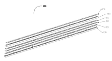
Traditionally, the lens for a one to one imaging optical scanner is a rod lens array. Please refer to FIG. 1, a perspective drawing of a prior-art rod lens array 100. The rod lens array 100 is constructed from a plurality of fiber optic rod lenses 110. Each individual fiber optic rod lens 110 is cut from a fiber optic glass strand, and its ends must be polished. The plurality of fiber optic rod lenses 110 are then arranged side by side, in a row or multiple rows with their optical axes in parallel, in a frame 120 and held in place by an adhesive layer 130. The fiber optic rod lenses 110 are typically made from GRIN (graduated index) fibers, with the refractive index of the glass carefully controlled during manufacture to have a graduated refractive index that decreases radially from the central axis to the edge.
However, this type of lens is expensive to manufacture. GRIN type fiber optic glass strands are expensive in and of themselves; cutting and polishing the strands to precise lengths to form fiber optic rod lenses 110, assembling them so that their axes are precisely parallel in the frame 120, and gluing the fiber optic rod lenses 110 are all precision steps for which entire technologies have had to be developed in order to satisfy requirements.
In addition, a major disadvantage of this type of lens is that because of the number of lenses and the difficulty in orienting them, it is not practical to shape the ends of the lenses so that they can magnify the surface that they are imaging; flat ends are used. In order to increase the imaging resolution, it is necessary to use larger numbers of smaller-diameter rod lenses 110, limiting the maximum resolution and driving up the costs as the desired resolution increases. Furthermore, suppliers for the necessary GRIN fiber optic strands are limited, and thus the base materials themselves are expensive.
Therefore there is need for an improved lens array for which materials are substantially cheaper and which is simpler to manufacture, and which can have increased resolution without substantially increasing costs.
SUMMARY OF THE INVENTION
To achieve these and other advantages and in order to overcome the disadvantages of the conventional method in accordance with the purpose of the invention as embodied and broadly described herein, the present invention provides a lens array where pluralities of lens faces are molded into surfaces of polymer bars, thus simplifying manufacturing, using inexpensive materials, and aligning the lenses without requiring significant manufacturing infrastructure.
The present invention further provides a lens array where the lens faces are configurable at the time of design to support increased resolution.
These and other objectives of the present invention will become obvious to those of ordinary skill in the art after reading the following detailed description of preferred embodiments.
It is to be understood that both the foregoing general description and the following detailed description are exemplary, and are intended to provide further explanation of the invention as claimed.
BRIEF DESCRIPTION OF THE DRAWINGS
The accompanying drawings are included to provide a further understanding of the invention, and are incorporated in and constitute a part of this specification. The drawings illustrate embodiments of the invention and, together with the description, serve to explain the principles of the invention. In the drawings:
FIG. 1 is a perspective drawing of a prior art rod lens array;
FIG. 2 is an exploded perspective drawing of a lens array of the present invention;
FIG. 3 a is a drawing of a surface of a stop for a lens array of the present invention with the view in line with the optical axis;
FIG. 3 b is a drawing of a surface of a spacer for a lens array of the present invention with the view in line with the optical axis;
FIG. 3 c is a drawing of a surface of a spacer for a lens array of the present invention with the view in line with the optical axis;
FIG. 4 a is a drawing of a first surface of a first lens section for a lens array of the present invention with the view in line with the optical axis;
FIG. 4 b is a drawing of a second surface of a first lens section for a lens array of the present invention with the view in line with the optical axis;
FIG. 4 c is a drawing of a cross-section of a first lens section for a lens array of the present invention along the long axis;
FIG. 5 is a drawing of a cross-section of a first lens section for a lens array of the present invention across a width of the first lens section;
FIG. 6 a is a drawing of a second surface of a first lens section for a lens array of the present invention with the view in line with the optical axis;
FIG. 6 b is a drawing of an end of a second surface of a first lens section for a lens array of the present invention with the view in line with the optical axis;
FIG. 6 c is a drawing of a cross-section of a first end of a first lens section for a lens array of the present invention along the long axis;
FIG. 6 d is a drawing of a cross-section of a second end of a first lens section for a lens array of the present invention along the long axis;
FIG. 7 a is a drawing of a first surface of a second lens section for a lens array of the present invention with the view in line with the optical axis;
FIG. 7 b is a drawing of a second surface of a second lens section for a lens array of the present invention with the view in line with the optical axis;
FIG. 7 c is a drawing of a cross-section of a second lens section for a lens array of the present invention along the long axis;
FIG. 8 a is a drawing of a first surface of a second lens section for a lens array of the present invention with the view in line with the optical axis;
FIG. 8 b is a drawing of a cross-section of an end of a second lens section for a lens array of the present invention along the long axis;
FIG. 9 is a drawing of a cross-section of a second lens section for a lens array of the present invention across a width of the second lens section;
FIG. 10 a is a detail drawing of a first end of a surface of a stop for a lens array of the present invention with the view in line with the optical axis;
FIG. 10 b is a detail drawing of a second end of a surface of a stop for a lens array of the present invention with the view in line with the optical axis;
FIG. 10 c is a detail drawing of an end of a surface of a spacer for a lens array of the present invention with the view in line with the optical axis;
FIG. 10 d is a detail drawing of an end of a surface of a spacer for a lens array of the present invention with the view in line with the optical axis;
FIG. 11 a is a perspective drawing of a lens array of the present invention;
FIG. 11 b is a drawing of a lens array of the present invention mounted to a printed circuit board, with the view in line with the optical axis;
FIG. 11 c is a cross-section drawing of a lens array of the present invention mounted to a printed circuit board, along the long axis;
FIG. 12 a is a top view of a lens array of the present invention in a frame mounted to a printed circuit board;
FIG. 12 b is a cross-section drawing of a lens array of the present invention in relation to a printed circuit board, along the long axis; and
FIG. 12 c is a cross-section drawing of a lens array of the present invention in relation to a printed circuit board, across the width of the lens array and printed circuit board.
DESCRIPTION OF THE PREFERRED EMBODIMENTS
Reference will now be made in detail to the preferred embodiments of the present invention, examples of which are illustrated in the accompanying drawings. Wherever possible, the same reference numbers are used in the drawings and the description to refer to the same or like parts.
Please refer to FIG. 2, which shows an exploded perspective drawing of a lens array of the present invention. The lens array 200 of this embodiment consists of a stop 240, a first lens section 210, three spacers 221,222,223, and a second lens section 230. Each component is discussed in further detail below. The number of spacers may vary between embodiments depending on design considerations. Only one spacer is required, but two or more may be used; the example embodiment uses three spacers. A frame (not shown) may optionally enclose the perimeter of the assembled lens array 200, providing support, mounting, and protection, and blocking external light.
Please refer momentarily to FIG. 6 b, which is a cross-section drawing of a lens array of the present invention in relation to a printed circuit board. This figure will be discussed in greater detail later; until then, note the distance 201 between the optical axes of two adjacent lens surfaces, referred to hereafter as the inter-axis distance 201.
Please refer to FIG. 3 a, which is a drawing of a surface of a stop for a lens array of the present invention with the view in line with the optical axis, in combination with FIG. 10 a and FIG. 10 b, which are detail drawings of the same part as marked in FIG. 3 a by A and B respectively. The stop 240 has a plurality of holes 241 organized such that the centers of the holes form a line down the center of the spacer. The first plurality of holes 241 are spaced apart equally by the inter-axis distance. The first plurality of holes 241 are circular, oval, cylindrical, or conical. Along the edges of the stop 240, a plurality of notches 242 is positioned to mate with a plurality of ears 211 e of the first surface 211 of the first lens section 210. A locating hole 243 near one end of the stop 240 is sized and positioned to fit around the phasing post 351 of the first lens array.
Please refer to FIG. 3 b, which is a drawing of a surface of a spacer for a lens array of the present invention with the view in line with the optical axis, in combination with FIG. 10 c, which is a detail of one end of the part as marked in FIG. 3 b by C. The third spacer 223 is substantially identical to the first spacer 221 and is not shown separately here. The first and third spacers 221,223 have a plurality of holes 410 organized such that the centers of the holes form a line down the center of the spacer. The holes 410 are spaced apart equally by one inter-axis distance 201. The holes 410 may be tapered right conic frustums or they may be cylindrical. Along the sides of the spacer 220, a plurality of notches 420 is positioned to mate with the ears 211 e of the lens arrays. A locating hole 430 near one end of the first and third spacers 221,223 is sized and positioned to fit around the phasing post 350 of the second lens array. The locating hole 430 and the plurality of notches 420 serve to locate and hold the first and third spacers 221,223 in alignment with the first and/or second lens sections 210,230 so that the centers of the holes 410 are centered on the lens axes. The minimum diameter of the holes 410 is the outer diameter of the lens faces molded into the surface against which the spacer is disposed.
FIG. 3 c is also a drawing of a surface of a spacer for a lens array of the present invention with the view in line with the optical axis, in combination with FIG. 10 d, which is a detail of the same part, noted in FIG. 3 c by D. The spacer 222 is similar to the first spacer 221 and third spacer 223 except that the diameter of the plurality of holes 411 are smaller. The plurality of holes 411 are spaced apart equally by one inter-axis distance 201. The notches 421 are the same size as the notches 420 of the spacers 221,223.
Please refer to FIG. 4 a, which is a drawing of a first surface of a first lens section for a lens array of the present invention with the view in line with the optical axis. Two section lines A-A and B-B are marked for use in FIG. 4 c and FIG. 5 respectively. FIG. 4 a shows the first surface 211 of the first lens section 210. The first surface 211 has a channel 211 c down the center of the lens, and a first plurality of lens surfaces 213 are formed with their optical axes in line, spaced apart equally by one inter-axis distance 201. The line of the centers of the first plurality of lens surfaces 213 in this example embodiment is along the center line of the channel 211 c. A plurality of ears 211 e is formed along the edges 211 a, 211 b of the first lens surface 211 of the first lens section 210, such that the ears 211 e are sized and spaced to mate with the notches 242 of the stop 240. The width of the first lens section 210 is substantially the same as the width of the stop 240. A first post 211 p is located at one end of the first lens section 210, sized and positioned to mate with the locating hole 243 of the stop 240. A surface of the stop 240 fits snugly against the faces of the edges 211 a, 211 b with notches 242 mating to ears 211 e so that the plurality of holes 241 of the stop 240 are lined up with their centers on the optical axes of the first plurality of lens surfaces 213. The locating hole 243 and the plurality of notches 242 serve to locate and hold the stop 240 in alignment with the first lens section 210 so that the centers of the holes 241 are substantially on the optical axes of the first plurality of lens surfaces 213.
Please refer to FIG. 4 b, which is a drawing of a second surface of a first lens section for a lens array of the present invention with the view in line with the optical axis, in combination with FIG. 6 a and FIG. 6 b, which are detail drawings of the same part as marked by C and D in FIG. 4 a, respectively. These figures show the second surface 212 of the first lens section 210. The second surface 212 has a channel 212 c down the center of the lens, and a second plurality of lens surfaces 214 are formed with their optical axes in line, spaced apart equally by one inter-axis distance 201. The line of the centers of the first plurality of lens surfaces 213 in this example embodiment is along the center line of the channel 212 c. A plurality of ears 212 e is formed along the edges 212 a, 212 b of the first lens surface 212 of the first lens section 210, such that the ears 212 e are sized and spaced to mate with the notches 420 of the first spacer 221. The width of the first lens section 210 is substantially the same as the width of the first spacer 221. A first hole 212 h is located and sized to mate with a second post 231 p (see FIG. 7 a, FIG. 7 c, and FIG. 8 b) of the second lens section 230 (see FIG. 7 a, FIG. 7 b, FIG. 7 c, FIG. 8 a, FIG. 8 b, and FIG. 9). A surface of the first spacer 221 fits snugly against the faces of the edges 212 a,212 b with notches 420 mating to ears 212 e so that the plurality of holes 410 are lined up with their centers on the optical axes of the second plurality of lens surfaces 214.
Please refer to FIG. 4 c, which is a drawing of a cross-section of a first lens section for a lens array of the present invention along the long axis, in combination with FIG. 6 c and FIG. 6 d, which are detail drawings of the same part for the details marked in FIG. 4 c by E and F respectively. The cross-section view also shows the distal portion of the lens in the background. The cross-section cuts across the first plurality of lens surfaces 213 and the second plurality of lens surfaces 214, as well as the first post 211 p and first hole 212 h. The second edges 211 b, 212 b and ears 211 e, 212 e are visible in the background, behind the channels 211 c, 212 c. In FIG. 6 c, a first post 211 p for positioning a stop 240 is located on the first surface 211. Several first lens surfaces of the first plurality of lens surfaces 213 are located in the channel 211 c. Several second lens surfaces of the second plurality of lens surfaces 214 are located in the channel 212 c. In FIG. 6 d, the first hole 212 h is located in the second surface 212. The plurality of optical axes of the first plurality of lens surfaces 213 are inline with the plurality of optical axes of the second plurality of lens surfaces 214. Please note that the optical axes of the second plurality of lens surfaces 214 are aligned with the optical axes of the first plurality of lens surfaces 213 and that the number of lens surfaces in the first plurality of lens surfaces 213 is the same as the number of lens surfaces in the second plurality of lens surfaces 214.
Please refer to FIG. 5, which is a cross-section drawing of a first lens section for a lens array of the present invention across a width of the first lens section. This cross-section cuts along the optical axes of a pair of lens surfaces consisting of one of the first plurality of lens surfaces 213 in channel 211 c and one of a lens surface of the second plurality of lens surfaces 214 in channel 212 c, two ears of the plurality of ears 211 e, and two ears of the plurality of ears 212 e. Visible in the background is the first post 211 p. Edges 211 a and 211 b, against which the stop 240 (not shown) will be placed when assembled, are shown. Edges 212 a and 212 b, against which the first spacer 221 will be placed when assembled, are also shown.
Please refer to FIG. 7 a, which is a drawing of a third surface of a second lens section for a lens array of the present invention with the view in line with the optical axis, in combination with FIG. 8 a, which is a detail of the same part for the region marked in FIG. 7 a by C. Two section lines A-A and B-B are marked for use in FIG. 7 c and FIG. 9 respectively. FIG. 7 a shows the third surface 211 of the second lens section 230. The third surface 231 has a channel 231 c down the center of the lens, and a third plurality of second lens surfaces 233 are formed with their optical axes in line, spaced apart equally by one inter-axis distance 201. The line of the centers of the third plurality of lens surfaces 233 in this example embodiment is along the center line of the channel 231 c. A plurality of ears 231 e is formed along the edges 231 a, 231 b of the second lens surface 231 of the second lens section 230, such that the ears 231 e are sized and spaced to mate with the notches 410 of the first spacer 221, the notches 411 of the second spacer 222, and the notches 410 of the third spacer 223. In this embodiment, the ears 231 e are substantially longer than the ears 212 e on the first lens section 210, and mate with the notches on all three spacers, compared with the first lens section 210 only mating with the notches on the first spacer 221, but this is implementation-dependent and may vary in practice. The width of the second lens section 230 is substantially the same as the width of the first spacer 221, second spacer 222, and third spacer 223. A second post 231 p is located at one end of the second lens section 230, sized and positioned to mate with the locating hole 430 of the first spacer 221, the locating hole 431 of the second spacer 222, the locating hole 430 of the third spacer 223, and the first hole 212 h of the first lens section 210. This second post 231 p is stepped down in diameter since the locating holes 430,431,430 are larger in diameter than the first hole 212 h (see further discussion for FIG. 8 b). A surface of the third spacer 223 fits snugly against the faces of the edges 231 a,231 b with notches 420 mating to ears 231 e so that the plurality of holes 410 are lined up with their centers on the optical axes of the third plurality of lens surfaces 233.
Please refer to FIG. 7 b, which is a drawing of a second surface of a second lens section for a lens array of the present invention with the view in line with the optical axis. FIG. 7 b shows the second surface 232 of the second lens section 230. The second surface 232 has a channel 232 c down the center of the lens, and a fourth plurality of lens surfaces 234 are formed with their optical axes in line, spaced apart equally by one inter-axis distance 201. The line of the centers of the third plurality of lens surfaces 233 in this example embodiment is along the center line of the channel 232 c. The edges to the sides 232 a, 232 b help protect the fourth plurality of lens surfaces 234 from handling damage during manufacture.
Please refer to FIG. 7 c, which is a drawing of a cross-section of a second lens section for a lens array of the present invention along the long axis, in combination with FIG. 8 b, which is a detail of the same part as marked in drawing 7 c by D. The cross-section view also shows the distal portion of the lens in the background. The cross-section cuts across the third plurality of lens surfaces 233 and the fourth plurality of lens surfaces 234, as well as the second post 231 p, which has a section of a first diameter 231 p 1 and a section of a second diameter 231 p 2. The section 231 p 1 is larger in diameter than the section 231 p 2; the section 231 p 1 is designed to mate with the locating holes 430,431,430 in the first spacer 221, second spacer 222, and third spacer 223 respectively. The section 231 p 2 is designed to mate with the first hole 212 h of the first lens section 210. The second edges 231 b, 232 b and ears 231 e are visible in the background, behind the channels 231 c, 232 c. Please note that the optical axes of the third plurality of lens surfaces 233 are aligned with the optical axes of the fourth plurality of lens surfaces 234 and that the number of lens surfaces in the third plurality of lens surfaces 233 is the same as the number of lens surfaces in the fourth plurality of lens surfaces 234.
Please refer to FIG. 11 a, a perspective drawing of a lens array of the present invention, in combination with FIG. 12 b and FIG. 12 c, cross sections of a lens array of the present invention. The lens array 200 is assembled with a frame 250 (not shown) so that it is held at a fixed distance from a sensor 260 which is mounted on a printed-circuit board (PCB) 270. The stop 240 is positioned against the first surface 211 of the first lens section 210. The first spacer 221 is positioned with one face against the second surface 212 of the first lens section 210, with its notches 420 aligned with and held in place by the ears 212 e, which extend only partially through the depth of the plurality of notches 420 of the first spacer 221; one face of the second spacer 222 is positioned against the other face of the first spacer 221; and then one face of the third spacer 223 is positioned against the other face of the second spacer 222; finally, the other face of the third spacer 223 is positioned against the third surface 231 of the second lens section 230. The second post 231 p of the second lens section 230 fits its larger-diameter segment 231 p 1 through the locating holes 430,431,430 of the first spacer 221, second spacer 222, and third spacer 223 respectively; and the longer ears 231 e of the second lens section 230 fit through the notches 420,421,420 of the first spacer 221, second spacer 222, and third spacer 223 respectively. The smaller-diameter segment 231 p 2 of the second post 231 p fits into the first hole 212 h of the second surface 212 of the first lens section 210. The ears 231 e of the second lens section 230 abut the ears of the first lens section 210. The ears, posts, holes, and notches combine to hold the stop 240, the three spacers 221,222,223, and the two lens sections 210,230 in alignment.
Referring now to FIG. 11 b, a top view of the lens array of the present invention assembled with a PCB, in combination with FIG. 12 a, a detail view of the same assembly, as marked on FIG. 11 b by B. A cross-section used in FIG. 11 c and FIG. 12 b is marked with the section line A-A. The lens array 200 is assembled inside a frame 250 which secures the lens to the PCB 270. The stop 240 is fitted against the first surface, and the first plurality of lens surfaces 213 of the first surface 211 of the first lens section 210 is visible through the plurality of holes 241 in the stop.
The lens surfaces of the first plurality of lens surfaces 213 have identical diameters and optical radii. The lens surfaces of the second plurality of lens surfaces 214 have identical diameters and optical radii. The lens surfaces of the third plurality of lens surfaces 233 have identical diameters and optical radii. The lens surfaces of the fourth plurality of lens surfaces 234 have identical diameters and optical radii. The four pluralities of lens surfaces 213,214,233,234 are identical in number and in the center-to-center spacing of the lens faces. The four pluralities of holes 410,411,410,241 from the first spacer 221, second spacer 222, third spacer 223, and stop 240 also are identical both in number and in the center-to-center spacing of the holes to the four pluralities of lens surfaces. As shown in FIG. 12 b, the optical axes of the four pluralities of lens surfaces, and the centers of the four pluralities of holes, are all aligned, thus forming a single plurality of lens units. Each quad of four lens faces, one from each of the four pluralities above, positioned on the same optical axis forms a lens unit with a lens axis. One embodiment for imaging A4 sized paper at 300 dpi has 330 lens units. Note that there is no restriction on the configuration of the lens units; although this example embodiment shows an array in a single line, two or more lines of lens units can be used, organized in a square grid, or a rectangular grid, or hexagonally.
Please refer to FIG. 11 c, a cross-section view of the lens array of the present invention assembled with a PCB, in combination with FIG. 12 b, a detail view of the same assembly, as marked on FIG. 11 c by C. A line at the top of FIG. 12 b represents the object plane 280, which corresponds to a surface to be imaged. The stop 240 is proximal to the object plane 280, along with the first plurality of lens surfaces 213. The plurality of lens surfaces gathers and focuses light reflected from the surface so that the light travels in a divergent beam through the first lens section to the second plurality of lens surfaces 214. The light is generated by an external source. The first spacer 221, second spacer 222, and third spacer 223 block and absorb scattered light, while the pluralities of holes 420,421,420 allow desired, focused light to reach the third plurality of lens surfaces 233. The light then transits the second lens section and exits through the fourth plurality of lens surfaces 234, which focuses the light onto the sensor 260 mounted on the PCB 270.
In the preferred embodiment, the first lens section and second lens section are preferably made of a refractive, substantially transparent polymer. The spacer(s), stop, and frame are preferably made of an opaque polymer, preferably black, to absorb and/or block undesirable scattered or external light. One or more spacers can be used; using fewer spacers reduces manufacturing costs. Use of a frame is optional.
The dots per inch (DPI) resolution of the lens array is adjustable at design time by changing the optical radii, conic constant, or aspherical coefficients of the four lens groups. In contrast with the prior art rod lenses, the lens array can be designed to magnify the surface being imaged. The lens surface is defined by the formula:
z = cy 2 1 + 1 - ( 1 + k ) c 2 y 2 + A 2 y 2 + A 4 y 4 + A 6 y 6 A 8 y 8 + A 10 y 10 ( eq 1 )
for each of the two lens sections.
The lens array thus provides a substantial improvement over the prior art by reducing manufacturing complexity and materials costs. Furthermore, the lens array makes it substantially less difficult to increase the resolution of a device using the lens array compared to the prior art.
It will be apparent to those skilled in the art that various modifications and variations can be made to the present invention without departing from the scope or spirit of the invention. In view of the foregoing, it is intended that the present invention cover modifications and variations of this invention provided they fall within the scope of the invention and its equivalent.

Claims (17)

1. A lens array comprising:
a first lens section, comprising a first surface and a second surface,
said first surface comprising a first plurality of lens surfaces, said first plurality of lens surfaces forming a first plurality of optical axes, said first plurality of lens surfaces having substantially the same size and shape,
said second surface comprising a second plurality of lens surfaces, said second plurality of lens surfaces forming a second plurality of optical axes, said second plurality of lens surfaces having substantially the same size and shape,
such that each optical axis of the first plurality of optical axes is aligned with an optical axis of the second plurality of optical axes;
a second lens section, comprising a third surface and a fourth surface,
said third surface comprising a third plurality of lens surfaces, said third plurality of lens surfaces forming a third plurality of optical axes, said third plurality of lens surfaces having substantially the same size and shape,
said fourth surface comprising a fourth plurality of lens surfaces, said fourth plurality of lens surfaces forming a fourth plurality of optical axes, said fourth plurality of lens surfaces having substantially the same size and shape,
such that each optical axis of the third plurality of optical axes is aligned with an optical axis of the fourth plurality of optical axes;
a spacer section, having a spacer thickness, comprising a first plurality of holes of circular cross section, said first plurality of holes having a first plurality of axes; and
a stop, having a stop thickness, comprising a second plurality of holes, said second plurality of holes having a second plurality of axes;
such that each optical axis of the second plurality of optical axes is aligned with an optical axis of the third plurality of optical axes, and each axis of the first plurality of axes is aligned with an optical axis of the third plurality of optical axes, and each axis of the second plurality of axes is aligned with an optical axis of the first plurality of optical axes; and
such that the stop is disposed against the first surface of the first lens section, the second surface of the first lens section is disposed against the first surface of the spacer section, and the second surface of the spacer section is disposed against the first surface of the second lens section.
2. The lens array of claim 1 where the first surface, the second surface, the third surface, and the fourth surface are substantially aspherical, and where the optical axes of the first plurality of optical axes are normal to a plane of the first surface, and where the optical axes of the first plurality of optical axes are arranged along a line such that a first distance between an adjacent pair of optical axes is substantially the same as another distance between any other adjacent pair of optical axes.
3. The lens array of claim 1 where the first lens section and the second lens section are formed from a substantially transparent polymer.
4. The lens array of claim 1 where the stop and the spacer section are formed from a substantially opaque black polymer.
5. The lens array of claim 1 where the first surface of the first lens section further comprises a first plurality of ears and a first locating post for positioning and holding in place the stop, and where the stop comprises a plurality of notches sized and positioned to mate with the first plurality of ears, and comprises a stop locating hole sized and positioned to mate with the first locating post.
6. The lens array of claim 1 where the second surface of the first lens section further comprises a second plurality of ears of a height less than the spacer thickness, and where the third surface of the second lens section further comprises a third plurality of ears of a height less than or equal to the height of the second plurality of ears minus the spacer thickness, and where the spacer section comprises a second plurality of notches sized and positioned to mate with both the second plurality of ears and the third plurality of ears, for locating and aligning the first lens section, the spacer section, and the second lens section.
7. The lens array of claim 1 where the second surface of the first lens section further comprises a lens locating hole, and where the third surface of the second lens section further comprises a locating post sized and positioned to mate with the lens locating hole, and where the spacer further comprises a spacer locating hole sized and positioned to mate around the locating post.
8. The lens array of claim 7 where:
the second surface of the first lens section further comprises a second plurality of ears;
the third surface of the second lens section further comprises a third plurality of ears;
the first spacer comprises a second plurality of notches sized and positioned to mate with the second plurality of ears, and comprises a first spacer locating hole sized and positioned to mate around the locating post; and
the second spacer comprises a third plurality of notches sized and positioned to mate with the second plurality of ears, and comprises a second spacer locating hole sized and positioned to mate around the locating post.
9. The lens array of claim 1 where the spacer section is comprised of a first spacer, a second spacer, and a third spacer, where:
the first spacer has a first surface against which the second surface of the first lens section is disposed;
the first spacer has a second surface against which the first surface of the second spacer is disposed;
the second spacer has a second surface against which the first surface of the third spacer is disposed;
the third spacer has a second surface against which the first surface of the second lens section is disposed;
the first spacer comprises a plurality of holes of a substantially same first diameter, the plurality of holes having a plurality of axes, each axis of which lies on an optical axis of the plurality of optical axes of the plurality of second lens surfaces;
the second spacer comprises a plurality of holes of a substantially same second diameter, the plurality of holes having a plurality of axes, each axis of which lies on an optical axis of the plurality of optical axes of the plurality of second lens surfaces; and
the third spacer comprises a plurality of holes of a substantially same third diameter, the plurality of holes having a plurality of axes, each axis of which lies on an optical axis of the plurality of optical axes of the plurality of second lens surfaces.
10. A lens array comprising:
a first lens section, comprising a first aspherical surface and a second planar surface,
said first aspherical surface comprising a first plurality of lens surfaces, said first plurality of lens surfaces forming a first plurality of optical axes normal to the first aspherical surface, said first plurality of lens surfaces having substantially the same size and shape,
said second planar surface comprising a second plurality of lens surfaces, said second plurality of lens surfaces forming a second plurality of optical axes, said second plurality of lens surfaces having substantially the same size and shape, such that each optical axis of the first plurality of optical axes is aligned with an optical axis of the second plurality of optical axes;
a second lens section, comprising a third aspherical surface and a fourth aspherical surface,
said third aspherical surface comprising a third plurality of lens surfaces, said third plurality of lens surfaces forming a third plurality of optical axes, said third plurality of lens surfaces having substantially the same size and shape,
said fourth aspherical surface comprising a fourth plurality of lens surfaces, said fourth plurality of lens surfaces forming a fourth plurality of optical axes, said fourth plurality of lens surfaces having substantially the same size and shape, such that each optical axis of the third plurality of optical axes is aligned with an optical axis of the fourth plurality of optical axes;
a spacer section, having a spacer thickness, comprising:
a first spacer, comprising a first surface, a second surface, and a plurality of holes of a substantially same first diameter, the plurality of holes having a plurality of axes, each axis of which lies on an optical axis of the second plurality of optical axes;
a second spacer, comprising a first surface, a second surface, and a plurality of holes of a substantially same second diameter, the plurality of holes having a plurality of axes, each axis of which lies on an optical axis of the second plurality of optical axes; and
a third spacer, comprising a first surface, a second surface, and a plurality of holes of a substantially same third diameter, the plurality of holes having a plurality of axes, each axis of which lies on an optical axis of the second plurality of optical axes, where:
the first surface of the second spacer is disposed against the second surface of the first spacer;
the first surface of the third spacer is disposed against the second surface of the second spacer; and
the second diameter is smaller than the first diameter, and the third diameter is substantially similar to the first diameter;
a stop, having a stop thickness, comprising a second plurality of holes, said second plurality of holes having a second plurality of axes;
such that each optical axis of the second plurality of optical axes is aligned with an optical axis of the third plurality of optical axes, and each axis of the first plurality of axes is aligned with an optical axis of the third plurality of optical axes, and each axis of the second plurality of axes is aligned with an optical axis of the first plurality of optical axes; and
such that the stop is disposed against the first surface of the first lens section, the second surface of the first lens section is disposed against the first surface of the first spacer of the spacer section, and the second surface of the third spacer of the spacer section is disposed against the first surface of the second lens section.
11. The lens array of claim 10 where the optical axes of the first plurality of optical axes are arranged along a line such that a first distance between an adjacent pair of optical axes is substantially the same as another distance between any other adjacent pair of optical axes.
12. The lens array of claim 10 where the first lens section and the second lens section are formed from a substantially transparent polymer.
13. The lens array of claim 10 where the stop and the spacer section are formed from a substantially opaque black polymer.
14. The lens array of claim 10 where the first surface of the first lens section further comprises a first plurality of ears and a first locating post for positioning and holding in place the stop, and where the stop comprises a plurality of notches sized and positioned to mate with the first plurality of ears, and comprises a stop locating hole sized and positioned to mate with the first locating post.
15. The lens array of claim 10 where the second surface of the first lens section further comprises a second plurality of ears of a height less than the spacer thickness, and where the third surface of the second lens section further comprises a third plurality of ears of a height less than or equal to the height of the second plurality of ears minus the spacer thickness, and where the spacer section comprises a second plurality of notches sized and positioned to mate with both the second plurality of ears and the third plurality of ears, for locating and aligning the first lens section, the spacer section, and the second lens section.
16. The lens array of claim 10 where the second surface of the first lens section further comprises a lens locating hole, and where the third surface of the second lens section further comprises a locating post sized and positioned to mate with the lens locating hole, and where the spacer further comprises a spacer locating hole sized and positioned to mate around the locating post.
17. The lens array of claim 16 where:
the second surface of the first lens section further comprises a second plurality of ears;
the third surface of the second lens section further comprises a third plurality of ears;
the first spacer comprises a second plurality of notches sized and positioned to mate with the second plurality of ears, and comprises a first spacer locating hole sized and positioned to mate around the locating post; and
the second spacer comprises a third plurality of notches sized and positioned to mate with the second plurality of ears, and comprises a second spacer locating hole sized and positioned to mate around the locating post.
US11/182,205 2005-07-15 2005-07-15 Lens array Active 2025-08-04 US7256941B2 (en)

Priority Applications (6)

Application Number Priority Date Filing Date Title
US11/182,205 US7256941B2 (en) 2005-07-15 2005-07-15 Lens array
TW095116057A TWI307779B (en) 2005-07-15 2006-05-05 Background of the invention
CNA2006100804361A CN1896789A (en) 2005-07-15 2006-05-16 Lens array
MYPI20063320A MY144356A (en) 2005-07-15 2006-07-12 Lens array
SG200604736A SG129389A1 (en) 2005-07-15 2006-07-13 Lens array
US11/773,834 US20080094717A1 (en) 2005-07-15 2007-07-05 Focus lens array with crosstalk reduction

Applications Claiming Priority (1)

Application Number Priority Date Filing Date Title
US11/182,205 US7256941B2 (en) 2005-07-15 2005-07-15 Lens array

Related Child Applications (1)

Application Number Title Priority Date Filing Date
US11/773,834 Continuation-In-Part US20080094717A1 (en) 2005-07-15 2007-07-05 Focus lens array with crosstalk reduction

Publications (2)

Publication Number Publication Date
US20070014022A1 US20070014022A1 (en) 2007-01-18
US7256941B2 true US7256941B2 (en) 2007-08-14

Family

ID=37609341

Family Applications (2)

Application Number Title Priority Date Filing Date
US11/182,205 Active 2025-08-04 US7256941B2 (en) 2005-07-15 2005-07-15 Lens array
US11/773,834 Abandoned US20080094717A1 (en) 2005-07-15 2007-07-05 Focus lens array with crosstalk reduction

Family Applications After (1)

Application Number Title Priority Date Filing Date
US11/773,834 Abandoned US20080094717A1 (en) 2005-07-15 2007-07-05 Focus lens array with crosstalk reduction

Country Status (5)

Country Link
US (2) US7256941B2 (en)
CN (1) CN1896789A (en)
MY (1) MY144356A (en)
SG (1) SG129389A1 (en)
TW (1) TWI307779B (en)

Cited By (1)

* Cited by examiner, † Cited by third party
Publication number Priority date Publication date Assignee Title
US11265437B2 (en) * 2019-12-12 2022-03-01 Canon Kabushiki Kaisha Lens array unit, image sensor unit, image reading apparatus, image forming apparatus, and method of manufacturing lens array unit

Families Citing this family (3)

* Cited by examiner, † Cited by third party
Publication number Priority date Publication date Assignee Title
CN102169196A (en) * 2010-02-25 2011-08-31 景传光电股份有限公司 Symmetrical lens array capable of improving view depth and enhancing uniformity and brightness
JP2015022291A (en) * 2013-07-23 2015-02-02 ニスカ株式会社 Image sensor unit and image reader
JP6488864B2 (en) * 2015-05-07 2019-03-27 三菱ケミカル株式会社 Method for manufacturing optical transmitter array

Citations (8)

* Cited by examiner, † Cited by third party
Publication number Priority date Publication date Assignee Title
US3605593A (en) * 1967-07-03 1971-09-20 Tektronix Inc Optical apparatus including a pair of mosaics of optical imaging elements
US5731899A (en) * 1996-12-20 1998-03-24 Eastman Kodak Company Lenslet array system incorporating an integral field lens/reimager lenslet array
US5796522A (en) * 1996-12-20 1998-08-18 Eastman Kodak Company Lenslet array system with a baffle structure and a shutter
US5812322A (en) * 1996-12-20 1998-09-22 Eastman Kodak Company Lenslet array system incorporating a field lenslet array
US5822125A (en) * 1996-12-20 1998-10-13 Eastman Kodak Company Lenslet array system
US5973844A (en) * 1996-01-26 1999-10-26 Proxemics Lenslet array systems and methods
US6124974A (en) * 1996-01-26 2000-09-26 Proxemics Lenslet array systems and methods
US6381072B1 (en) * 1998-01-23 2002-04-30 Proxemics Lenslet array systems and methods

Family Cites Families (4)

* Cited by examiner, † Cited by third party
Publication number Priority date Publication date Assignee Title
US4168900A (en) * 1978-04-24 1979-09-25 Minolta Camera Kabushiki Kaisha Compact erect optical imaging copier system and method
US6545811B1 (en) * 1999-01-29 2003-04-08 Rohm Co., Ltd. Lens unit for image formation, and image reader having lens unit
US6707613B2 (en) * 2000-04-05 2004-03-16 Rohm Co., Ltd. Lens array unit and method of forming image
US6646807B2 (en) * 2001-06-19 2003-11-11 Rohm Co., Ltd. Lens array unit and process for making lens array

Patent Citations (8)

* Cited by examiner, † Cited by third party
Publication number Priority date Publication date Assignee Title
US3605593A (en) * 1967-07-03 1971-09-20 Tektronix Inc Optical apparatus including a pair of mosaics of optical imaging elements
US5973844A (en) * 1996-01-26 1999-10-26 Proxemics Lenslet array systems and methods
US6124974A (en) * 1996-01-26 2000-09-26 Proxemics Lenslet array systems and methods
US5731899A (en) * 1996-12-20 1998-03-24 Eastman Kodak Company Lenslet array system incorporating an integral field lens/reimager lenslet array
US5796522A (en) * 1996-12-20 1998-08-18 Eastman Kodak Company Lenslet array system with a baffle structure and a shutter
US5812322A (en) * 1996-12-20 1998-09-22 Eastman Kodak Company Lenslet array system incorporating a field lenslet array
US5822125A (en) * 1996-12-20 1998-10-13 Eastman Kodak Company Lenslet array system
US6381072B1 (en) * 1998-01-23 2002-04-30 Proxemics Lenslet array systems and methods

Cited By (1)

* Cited by examiner, † Cited by third party
Publication number Priority date Publication date Assignee Title
US11265437B2 (en) * 2019-12-12 2022-03-01 Canon Kabushiki Kaisha Lens array unit, image sensor unit, image reading apparatus, image forming apparatus, and method of manufacturing lens array unit

Also Published As

Publication number Publication date
TWI307779B (en) 2009-03-21
MY144356A (en) 2011-09-15
TW200702716A (en) 2007-01-16
SG129389A1 (en) 2007-02-26
US20080094717A1 (en) 2008-04-24
CN1896789A (en) 2007-01-17
US20070014022A1 (en) 2007-01-18

Similar Documents

Publication Publication Date Title
US20100124063A1 (en) Miniturized linear light source sub-module for various format main modules
US20050128597A1 (en) Image pickup lens unit and image pickup device
US20050030647A1 (en) Image pickup lens unit and image pickup device
US8485738B2 (en) Optical fiber connector
KR970068686A (en) Image Display Device
JPH08220307A (en) Optical system
US7256941B2 (en) Lens array
JP2013037298A (en) Erecting life-size lens array plate
US20100238520A1 (en) Erecting equal-magnification lens array plate, optical scanning unit, and image reading device
JP2000221442A (en) Image-formation optical device
US20030133687A1 (en) Integration of array of non-rod shaped optical elements with array of fibers in a structure and associated methods
JPH04274201A (en) Lens array
EP2383592B1 (en) Two dimensional fiber collimator array with low back reflections
KR100225163B1 (en) Photoelectric detector for a register control device within a torary printing machine
US7869137B2 (en) ABBE prism lens with improved focus and reduced flair
JP2003279871A (en) Optical connection module and optical system for infrared light ray
US20030152325A1 (en) Optical module
EP2455783B1 (en) Abbe prism lens with improved focus and reduced flare
JPS61226701A (en) Lens array
EP2362245B1 (en) Symetrical lens array with improved depth of field, enhanced uniformity, and brightness
US20040052494A1 (en) Optical fiber array and optical fiber collimator array and optical module using the same
US20100046081A1 (en) Symetrical lens array with improved depth of field, enhanced uniformity, and brightness
JP2004101848A (en) Microlens array, optical module using microlens array and method for positioning optical module
EP1635204A1 (en) Glass fibre with integrated diffractive element on the top of its end face
TWI432816B (en) Symmetric lens array with improved depth of field, enhanced uniformity, and brightness

Legal Events

Date Code Title Description
AS Assignment

Owner name: PIXON TECHNOLOGIES CORP., TAIWAN

Free format text: ASSIGNMENT OF ASSIGNORS INTEREST;ASSIGNORS:WU, RONG YAW;CHEN, SHENG LI;CHEN, SHIH CHE;REEL/FRAME:016788/0205

Effective date: 20050714

STCF Information on status: patent grant

Free format text: PATENTED CASE

FPAY Fee payment

Year of fee payment: 4

FPAY Fee payment

Year of fee payment: 8

MAFP Maintenance fee payment

Free format text: PAYMENT OF MAINTENANCE FEE, 12TH YR, SMALL ENTITY (ORIGINAL EVENT CODE: M2553); ENTITY STATUS OF PATENT OWNER: SMALL ENTITY

Year of fee payment: 12