US7265892B2 - Micromirror array devices with light blocking areas - Google Patents
Micromirror array devices with light blocking areas Download PDFInfo
- Publication number
- US7265892B2 US7265892B2 US11/120,814 US12081405A US7265892B2 US 7265892 B2 US7265892 B2 US 7265892B2 US 12081405 A US12081405 A US 12081405A US 7265892 B2 US7265892 B2 US 7265892B2
- Authority
- US
- United States
- Prior art keywords
- light
- layer
- substrate
- light blocking
- posts
- Prior art date
- Legal status (The legal status is an assumption and is not a legal conclusion. Google has not performed a legal analysis and makes no representation as to the accuracy of the status listed.)
- Active, expires
Links
Images


Classifications
-
- G—PHYSICS
- G02—OPTICS
- G02B—OPTICAL ELEMENTS, SYSTEMS OR APPARATUS
- G02B26/00—Optical devices or arrangements for the control of light using movable or deformable optical elements
- G02B26/08—Optical devices or arrangements for the control of light using movable or deformable optical elements for controlling the direction of light
- G02B26/0816—Optical devices or arrangements for the control of light using movable or deformable optical elements for controlling the direction of light by means of one or more reflecting elements
- G02B26/0833—Optical devices or arrangements for the control of light using movable or deformable optical elements for controlling the direction of light by means of one or more reflecting elements the reflecting element being a micromechanical device, e.g. a MEMS mirror, DMD
- G02B26/0841—Optical devices or arrangements for the control of light using movable or deformable optical elements for controlling the direction of light by means of one or more reflecting elements the reflecting element being a micromechanical device, e.g. a MEMS mirror, DMD the reflecting element being moved or deformed by electrostatic means
-
- H—ELECTRICITY
- H04—ELECTRIC COMMUNICATION TECHNIQUE
- H04N—PICTORIAL COMMUNICATION, e.g. TELEVISION
- H04N9/00—Details of colour television systems
- H04N9/12—Picture reproducers
- H04N9/31—Projection devices for colour picture display, e.g. using electronic spatial light modulators [ESLM]
- H04N9/3102—Projection devices for colour picture display, e.g. using electronic spatial light modulators [ESLM] using two-dimensional electronic spatial light modulators
- H04N9/3111—Projection devices for colour picture display, e.g. using electronic spatial light modulators [ESLM] using two-dimensional electronic spatial light modulators for displaying the colours sequentially, e.g. by using sequentially activated light sources
- H04N9/3114—Projection devices for colour picture display, e.g. using electronic spatial light modulators [ESLM] using two-dimensional electronic spatial light modulators for displaying the colours sequentially, e.g. by using sequentially activated light sources by using a sequential colour filter producing one colour at a time
Definitions
- the present invention is generally related to the art of micromirror array devices, and more particularly, to the micromirror array devices with light blocking areas for reducing unwanted light scattering.
- Projection display systems employing spatial light modulators, as well as many other image-reproducing systems prefer only image-data encoded light to be projected on the viewing screens so as to obtain the desired images or videos of pleasant display quality.
- Non-image data encoded light such as ambient light and light scattered from the members of the micromirror array devices can degrade the display quality if projected also on the viewing screen and superpositioned with the image-data encoded light. In particular, such superposition may significantly decrease the contrast ratio of the displayed image.
- Contrast ratio is the ratio of luminance between the brightest white that can be produced and the darkest black that can be produced. If a display image has a higher contrast ratio, a viewer will judge it to be sharper than a displayed image with a lower contrast ratio, even if the lower contrast image has substantially more measurable resolution.
- the present invention teaches a micromirror array device having a light blocking provided for reducing light scattering from the posts of the micromirror array devices.
- a light blocking pad is provided for a post of the micromirror array device.
- Such light blocking pad can be a light absorbing film that absorbs 90% or more, or preferably 99% or more of the light incident thereto.
- the light blocking pad can be a light reflective film that reflects 90% or more, or preferably 99% or more of the light incident thereto.
- the light blocking pad is preferably formed such that the incident light is directed towards a corner of the pad.
- the shape of the pad can be independent of the shape of the exposed area of the posts, but preferably covers the entire exposed area of the posts—that is, the post may have no edges parallel to the edges of the post.
- the light blocking pad may have no edges parallel to the edges of the micromirror array either.
- the light blocking area may be formed such that the pad comprises an edge that is parallel to an edge of the post or the mirror plate that is held by the post, or is parallel to an edge of the micromirror array.
- the micromirror array device can be formed by providing a substrate and depositing a first sacrificial layer on the substrate.
- the sacrificial layer is then patterned followed by depositing and patterning of an array of mirror plates.
- the second sacrificial layer is then deposited and patterned followed by a process of forming the hinge contact, posts, and light blocking areas as appropriate such that each post has a light blocking area disposed between a surface of the post and the substrate.
- an array of light blocking pads can be formed on the substrate before depositing the first sacrificial layer and the subsequent fabrication processes for the other fabrication layers of the micromirror array devices.
- FIG. 1 illustrates an exemplary display system employing a spatial light modulator in which embodiment of the invention can be implemented
- FIG. 2 illustrates another exemplary display system employing more than one spatial light modulators in each of which embodiment of the invention can be implemented;
- FIG. 3 is a cross-sectional view of an exemplary spatial light modulator usable for the display systems in FIG. 1 and FIG. 2 ;
- FIG. 4 schematically illustrates a photo of the micromirror array device without the light blocking pads of the invention
- FIG. 5 a and FIG. 5 b demonstratively illustrate examples of positioning a light blocking pad in relation to the incident light
- FIG. 7 illustrates a micromirror device of the micromirror array device of FIG. 3 ;
- FIG. 8 illustrates an exemplary micromirror device according an embodiment of the invention
- FIG. 9 illustrates a top view of the reflective and deflectable mirror plate in relation to the rotation axis of the micromirror device in FIG. 8 ;
- FIG. 10 illustrates another exemplary micromirror device according an embodiment of the invention.
- FIG. 11 illustrates a top view of the reflective and deflectable mirror plate in relation to the rotation axis of the micromirror device in FIG. 10 ;
- FIG. 12 illustrates a perspective view of an exemplary spatial light modulator according to an embodiment of the invention
- FIG. 13 illustrates a top view of another exemplary spatial light modulator according to another embodiment of the invention.
- FIG. 14 illustrates a top view of yet another exemplary spatial light modulator according to another embodiment of the invention.
- FIG. 15 illustrates a top view of yet another exemplary spatial light modulator according to another embodiment of the invention.
- FIG. 16 a to FIG. 16 c illustrate a top view of yet another exemplary spatial light modulator according to another embodiment of the invention.
- FIG. 17 illustrates a top view of yet another exemplary spatial light modulator according to yet another embodiment of the invention.
- FIG. 18 a to 18 c are cross-sectional views of a micromirror device in FIG. 5 . in an exemplary fabrication process.
- the present invention discloses a micromirror array device having a light blocking area for reducing unexpected light scattering.
- the present invention will be discussed with reference to selected examples from many possible variations thereof. It will be immediately understood by those skilled in the art that the following discussion is for demonstration purposes only, and should not be interpreted as a limitation.
- FIG. 1 schematically illustrates an exemplary display system that employs a spatial light modulator in which embodiment of the invention can be implemented.
- display system 100 comprises light source illumination system 116 , group lens 108 , spatial light modulator 110 , projection lens 112 , and display target 114 .
- the illumination system may further comprise light source 102 , light pipe 104 , and color filter 106 such as a color wheel.
- the color wheel can also be positioned between the light source and light pipe at the propagation path of the illumination light.
- the illumination light can be polarized or non-polarized.
- display target 114 may comprise a polarization filter associated with the polarized illumination light, as set forth in U.S. provisional patent application Ser. No. 60/577,422 filed Jun. 4, 2004, the subject matter being incorporated herein by reference.
- the light source can be any suitable light source, such as an arc lamp, preferably an arc lamp with a short arc for obtaining intensive illumination light.
- the light source can also be an arc lamp with a spiral reflector, as set forth in U.S. patent application Ser. No. 11/055,654 filed Feb. 9, 2005, the subject matter being incorporated herein by reference.
- the lightpipe ( 104 ) can be a standard lightpipe that are widely used in digital display systems for delivering homogenized light from the light source to spatial light modulators.
- the lightpipe can be the one with movable reflective surfaces, as set forth in U.S. patent provisional application Ser. No. 60/620,395 filed Oct. 19, 2004, the subject matter being incorporated herein by reference.
- the color wheel ( 106 ) comprises a set of color and/or white segments, such as red, green, blue, or yellow, cyan, and magenta.
- the color wheel may further comprise a clear or non-clear segment, such as a high throughput or white segment for achieving particular purposes, as set forth in U.S. patent application Ser. No. 10/899,637, and Ser. No. 10/899,635 both filed Jul. 26, 2004, the subject matter of each being incorporated herein by reference, which will not be discussed in detail herein.
- the display system in FIG. 1 employs one spatial light modulator. However, a display system may use multiple spatial light modulators for modulating the illumination light of different colors.
- a display system may use multiple spatial light modulators for modulating the illumination light of different colors.
- One of such display systems is schematically illustrated in FIG. 2 .
- the display system uses a dichroic prism assembly 204 for splitting incident light into three primary color light beams.
- Dichroic prism assembly comprises TIR 176 a , 176 c , 176 d , 176 e and 176 f .
- Totally-internally-reflection (TIR) surfaces i.e. TIR surfaces 205 a and 205 b , are defined at the prism surfaces that face air gaps.
- the surfaces 198 a and 198 b of prisms 176 c and 176 e are coated with dichroic films, yielding dichroic surfaces.
- dichroic surface 198 a reflects green light and transmits other light.
- Dichroic surface 198 b reflects red light and transmits other light.
- the three spatial light modulators, 182 , 184 and 186 each having a micromirror array device, are arranged around the prism assembly.
- incident white light 174 from light source 102 enters into TIR 176 a and is directed towards spatial light modulator 186 , which is designated for modulating the blue light component of the incident white light.
- the green light component of the totally internally reflected light from TIR surface 205 a is separated therefrom and reflected towards spatial light modulator 182 , which is designated for modulating green light.
- the separated green light may experience TIR by TIR surface 205 b in order to illuminate spatial light modulator 182 at a desired angle. This can be accomplished by arranging the incident angle of the separated green light onto TIR surface 205 b larger than the critical TIR angle of TIR surface 205 b .
- the spatial light modulators of the display systems in FIG. 1 and FIG. 2 each comprise a micromirror array device having an array of reflective deflectable mirror plates.
- An example of such spatial light modulators is illustrated in a cross-sectional view in FIG. 3 .
- spatial light modulator comprises light transmissive substrate 210 and semiconductor substrate 212 .
- the two substrates together form a gap therebetween in which an array of reflective deflectable mirror plates (e.g. mirror plate 216 of micromirror device 214 ) are disposed.
- an array of addressing electrodes e.g. addressing electrode 218 of micromirror device 214
- addressing electrodes e.g. addressing electrode 218 of micromirror device 214
- the reflective deflectable mirror plates are disposed within the gap between substrates 210 and 212 , and can be formed on either one of the substrates.
- substrate 210 is a light transmissive substrate such as glass, quartz, or sapphire
- substrate 212 is a standard semiconductor silicon substrate on which standard integrated circuits can be fabricated.
- the mirror plates are formed on the light transmissive substrate. Specifically, each mirror plate such as mirror plate 216 is connected to and thus held on substrate 210 by a post (e.g. post 224 ). Alternatively, the mirror plates can be formed on the same substrate as the addressing electrodes, such as substrate 212 .
- an array of posts are formed on substrate 212 with each of the posts connecting one of the mirror plate to substrate 212 , which is not shown in the figure.
- the mirror plates can be derived from a single crystal, such as single crystal silicon, and are connected to substrate 212 via posts that are formed on substrate 212 , as set forth in U.S. patent application Ser. No. 11/056,732, Ser. No. 11/056,727, now U.S. Pat. No. 7,119,944 and Ser. No. 11/056,752, all filed on Feb. 11, 2005, the subject matter of each being incorporate herein by reference.
- substrate 210 may or may not be necessary.
- a portion of the posts is exposed to the incident light.
- a disadvantage of such exposure is unexpected light scattering of the incident light from the exposed portion of the posts.
- the top surface of each post contacting substrate 210 is exposed to the incident light, which results in light scattering.
- the scattered light superposes with the displayed image on the viewing screen, resulting in unpleasant viewing effects.
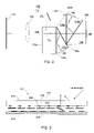
- An exemplary illumination pattern generated by the scattered light is schematically illustrated in FIG. 4 .
- open circles, such as open circles 220 are images of the exposed areas of the posts and are generated by the scattered light. Dark spots are images of other exposed portions of the micromirror devices, such as the mirror plate corners. Such illumination pattern overlaps with the displayed image and degrades the image quality of the displayed image.
- An approach to solve this problem is providing light blocking pads to cover the exposed areas of the posts, such as light blocking pad 226 in mirror device 214 shown in FIG. 3 .
- a light blocking pad is disposed between each post and substrate 210 so as to reduce the light scattering from the exposed area of the post.
- the light blocking pads can be in any suitable shapes but each preferably covers the entire exposed area of the posts—that is, the shapes of the light blocking pads may or may not be configured independently from the shapes of the exposed areas of the posts.
- the light blocking pads may also introduce unpleasant light scattering.
- the light blocking pads each can be shaped such that the illumination light to be modulated by the micromirror array device is directed towards a corner of the light blocking pad. More preferably, no edge of the light blocking pad is perpendicular to the propagation path of the illumination light, as shown in FIGS. 5 a and 5 b.
- the light blocking pad can be square in shape.
- the illumination impinges the light blocking pad at a corner of the light blocking pad when viewed from the above of the light blocking pad.
- the illumination light is neither parallel nor perpendicular to any edge of the square shaped light blocking pad.
- the incident light illuminates the light blocking pad at an angle to the surface of the light blocking pad.
- the light blocking pads can be configured independently from the mirror plates or the micromirror array. However, because the direction of the illumination light is preferably towards the corners of the mirror plates so as to reduce the light scattering from the edges of the mirror plates; and so as for the light blocking pads as discussed above with reference to FIG. 5 a and FIG. 5 b , the light blocking pad and mirror plate can be aligned to each other.
- FIG. 6 An example of such configuration is shown in FIG. 6 .
- post 219 is disposed at a corner of mirror plate 217 for supporting the mirror plate on a substrate (not shown in the figure).
- the exposed surface of the post is covered by light blocking pad 225 (superposed on the exposed surface of the post) so as to reduce the light scattering therefrom.
- the incident light is directed towards a corner of the mirror plate and corner of the light blocking pad.
- the incident light is neither parallel nor perpendicular to any one of the edges of the mirror plate and light blocking pad.
- each post be provided with a light blocking pad to reduce the light scattering therefrom, this is not an absolute requirement.
- some of the exposed areas of the posts may be covered with light blocking pads, while one or more of the exposed areas are not. This becomes important especially when the light blocking pads are regularly repeated across the entire micromirror array and generate an image of the regular disposure on the viewing screen.
- the light blocking pad may comprise a light absorbing material that absorbs 85% or more, or 90% or more, or 99% or more of the illumination light incident thereto.
- the light blocking pad may be composed of a light reflective material that reflects 85% or more, or 90% or more, or 99% or more of the illumination light incident thereto.
- the light blocking pads each can be a single layer or a multilayered structure.
- the light absorbing material is preferably one that absorbs wavelengths of broad range in the visible spectrum.
- An opaque material, preferably a black material is preferred. More specifically, the non-reflective material can be a dark, opaque (e.g. black, grey, or other dark colors) thin film.
- the light absorbing material comprises Chromium or chromium oxide
- suitable materials such as black nickel, CrN x , TiAl x , TaN x , and materials containing carbon, such as amorphous CN x , amorphous CAlN y , CTi x N y , a-DLC, vitreous carbon, SiC, TiAlCN, WC, etc, are also applicable.
- Multilayer structures such as TiC/WC, WC/C or TiAln/WC/C, can be used, as well as other multilayer structures with matched indices.
- polymides and other polymers containing carbon black (or other opacity increasing material) can be used.
- the light absorbing layer is exposed to an etchant at the time of release of the micromirrors, the light absorbing material should preferably be resistant to the etchant used.
- other opaque films preferably those with high optical density, thermally stable and with low reflectivity
- the light absorbing material can be deposited as a thin film using suitable standard thin film deposition techniques, such as electroplating, PVD, CVD, PECVD, sputtering, and CMP (chemical mechanical polarization).
- suitable standard thin film deposition techniques such as electroplating, PVD, CVD, PECVD, sputtering, and CMP (chemical mechanical polarization).
- the light absorbing thin film may have a thickness in an order of microns or less, such as 100 microns or less, 50 microns or less, 10 microns or less, or several microns or even less.
- FIG. 7 a cross-sectional view of a micromirror device having a light blocking pad on the post of the micromirror device is illustrated in FIG. 7 .
- substrate 210 is a light transmissive substrate
- substrate 212 is a standard semiconductor substrate such as a silicon substrate.
- Post 224 is formed on substrate 210 with light blocking pad 226 being disposed therebetween.
- Hinge support 230 is connected to and thus held by post 224 .
- a deformable hinge is affixed to the hinge support.
- Reflective deflectable mirror plate 234 is attached to the deformable hinge via hinge contact 228 such that the mirror plate is capable of rotating relative substrate 210 , such as to the ON and OFF state as shown in the figure.
- addressing electrode 236 formed on substrate 212 and disposed proximate to the mirror plate.
- the addressing electrode is preferably disposed beyond the area of the mirror plate, as set forth in U.S. patent application Ser. No. 10/947,005 filed Sep. 21, 2004, now U.S. Pat. No. 7,113,322 the subject matter being incorporated herein by reference.
- the mirror plate is associated with only one addressing electrode (e.g. addressing electrode 236 ).
- another electrode such as electrode 222 can be provided for rotating the mirror plate towards substrate 210 .
- electrode 222 is formed on light transmissive substrate 210 , it is preferred that electrode 222 is electrically conductive and is transmissive to the incident light.
- An example of such electrode can be a thin film of indium-tin-oxide.
- Electrode 222 can also be a multi-layered structure.
- electrode 222 may comprise an electrically conductive layer and electrically non-conductive layer with the electrically conductive layer being sandwiched between substrate 210 and the electrically non-conductive layer. This configuration prevents potential electrical short between the mirror plate and electrode 222 .
- the electrically non-conductive layer can be SiO x , TiO x , SiN x , and NbO x , as set forth in U.S. patent application Ser. No. 11/102,531 filed Apr. 8, 2005, the subject matter being incorporated herein by reference.
- multiple addressing electrodes can be provided for the micromirror device, as set forth in U.S. patent application Ser. No. 10/437,776 filed May 13, 2003, now U.S. Pat. No. 7, 099,065 and Ser. No. 10/947,005 filed Sep. 21, 2004, the subject matter of each being incorporated herein by reference in entirety.
- Stopper 232 can provided as an alternative feature to limit the rotation of the mirror plate in accordance with the operation states, such as the ON state when the micromirror is operated in a binary mode including the ON and OFF state.
- the stopper can be formed in many alternative ways, such as those set forth in U.S. patent application Ser. No. 10/437,776 filed Apr. 13, 2003 and Ser. No. 10/613,379 filed Jul. 3, 2003, now U.S. Pat. No. 6,873,450 Ser. No. 10/703,678 filed Nov. 7, 2003, now U.S. Pat. No. 6,876,485 the subject matter of each being incorporated herein by reference.
- optical coatings on the light transmissive substrate 210 for adjusting the optical properties of the light transmissive substrate.
- an anti-reflection layer can be formed on a surface of the light transmissive substrate 210 for enhancing the transmission of the illumination light.
- Such optical coating can be a single or a multilayered structure.
- optical indices of the electrically conductive and electrically non-conductive layers, as well as the optical indices of the optical coating layers can be optimized so as to achieve optimum effect in both electrical and optical properties.
- the optical coating can be arranged such that the electrically conductive layer is isolated from the mirror plate by an electrically non-conductive layer, and the laminate combination of all layers results in a gradient of optical indices from the surface of the light transmissive substrate to the outmost layer of the laminate combination layers.
- An exemplary of such laminate combination incorporating both electrical and optical properties can be a SiO x -ITO (indium-tin-oxide)-SiO x -TiO x /NbO x film group.
- the micromirror device as show in FIG. 7 is only one example of many applicable examples of the invention.
- the mirror plate is attached to the deformable hinge such that the mirror plate rotates asymmetrically. That is the maximum rotation angle (e.g. the ON state angle) achievable by the mirror plate rotating in one direction (the direction towards the ON state) is larger than that (e.g. the OFF stat angle) in the opposite rotation direction (e.g. the direction towards the OFF state).
- This is accomplished by attaching the mirror plate to the deformable hinge at a location that is not at the center of the mirror plate such that the rotation axis of the mirror plate is offset from a diagonal of the mirror plate.
- the rotation axis may or may not be parallel to the diagonal.
- the mirror plate can be attached to the deformable hinge such that the mirror plate rotates symmetrically. That is the maximum angle achievable by rotating the mirror plate is substantially the same as that in the opposite rotation direction.
- the mirror plate of the micromirror shown in FIG. 7 can be attached to the deformable hinge such that the mirror plate and deformable hinge are in the same plane.
- the deformable hinge can be located in a separate plane as the mirror plate when viewed from the top of the mirror plate at a non-deflected state, which will not be discussed in detail herein.
- Micromirror device 238 comprises substrate 210 that is a light transmissive substrate such as glass, quartz, and sapphire and semiconductor substrate 182 , such as silicon substrate.
- Deflectable and reflective mirror plate 240 is spaced apart and attached to deformable hinge 242 via a hinge contact.
- the deformable hinge is affixed to and held by posts 244 .
- the semiconductor substrate has addressing electrode 248 for deflecting the mirror plate.
- Light blocking pad 246 is formed between the surface of post 244 and substrate 210 for reducing unexpected light scattering from the exposed surface of the posts.
- FIG. 9 A top view of the micromirror in FIG. 8 is illustrated in FIG. 9 .
- deformable hinge 252 is not along but offset from the symmetrical axis OO′ of the mirror plate such that the mirror plate is operable to rotate asymmetrically.
- the deformable hinge is located beneath the mirror plate in the direction of the incident light. That is, the mirror plate is located between the light transmissive substrate and the deformable hinge such that the deformable hinge is not illuminated by the incident light so as to prevent unexpected light scattering from the deformable hinge, thereby, increasing the contrast ratio of the produced image.
- the quality of the produced image is further improved through reduction of the light scattering from the edges of the mirror plate by forming the edges of the mirror plate into a zigzag shape, as shown in the figure.
- the deflectable and reflective mirror plate can be a multilayered structure.
- the mirror plate may comprise an electrical conducting layer, a reflective layer that is capable of reflecting 85% or more, or 90% or more, or 85% or more, or 99% or more of the incident light (e.g. incident visible light), a mechanical enhancing layer that enhances the mechanical properties of the mirror plate.
- An exemplary mirror plate can be a multilayered structure comprising a SiO 2 layer, an aluminum layer, a titanium layer, and a titanium nitride layer. When aluminum is used for the mirror plate; and amorphous silicon is used as the sacrificial material, diffusion between the aluminum layer and the sacrificial material may occur. This can be avoided by depositing a barrier layer therebetween.
- FIG. 10 Another exemplary micromirror device having a cross-sectional view of FIG. 7 is illustrated in its perspective view in FIG. 10 .
- deflectable reflective mirror plate 254 with a substantially square shape is formed on light transmissive substrate 210 , and is attached to deformable hinge 256 via hinge contact 258 .
- the deformable hinge is held by hinge support 260 , and the hinge support is affixed and held by posts on the light transmissive substrate.
- an addressing electrode (not shown in the figure for simplicity purposes) is fabricated in the semiconductor substrate 212 .
- extending metallic plate 266 can be formed on the mirror plate and contacted to the mirror plate via post 264 .
- Light blocking pad 268 is disposed between the surface of the post and substrate 210 so as to reduce unexpected light scattering from the post.
- the light blocking pad can also be deployed in a way so as to block light scattered from other portions of the micromirror, such as the tips (or the corners) of the mirror plate of the micromirror, and the exterior surfaces (e.g. the walls) of the posts.
- the mirror plate is preferably attached to the deformable hinge asymmetrically such that the mirror plate can be rotated asymmetrically for achieving high contrast ratio.
- the asymmetric attachment is better illustrated in FIG. 11 .
- mirror plate comprises diagonals BB and CC.
- Deformable hinge is disposed with its length parallel to a diagonal (e.g. BB) of the mirror plate.
- the length of the deformable is not along any diagonal of the mirror plate in the top view when the mirror plate is parallel to the light transmissive substrate.
- the mirror plate can be attached to the deformable hinge symmetrically by placing the attachment point around the geometric or mass center of the mirror plate, which will not be discussed in detail herein.
- the deformable hinge is preferably formed beneath the deflectable mirror plate in the direction of the incident light so as to avoid unexpected light scattering by the deformable hinge.
- the illumination light is preferably incident onto the mirror plate along a corner of the mirror plate.
- the micromirror array of a spatial light modulator consists of thousands or millions of micromirrors, the total number of which determines the resolution of the displayed images.
- the micromirror array of the spatial light modulator may have 1024 ⁇ 768, 1280 ⁇ 720, 1400 ⁇ 1050, 1600 ⁇ 1200, 1920 ⁇ 1080, or even larger number of micromirrors. In other applications, the micromirror array may have less number of micromirrors.
- the array of deflectable reflective mirror plates 276 is disposed between light transmissive substrate 272 and semiconductor substrate 274 having formed thereon an array of addressing electrodes 278 each of which is associated with a mirror plate for electrostatically deflecting the mirror plate.
- the posts of the micromirrors are covered by light blocking pads 280 for reducing expected light scattering from the surfaces of the posts.
- the illumination light passes through the light transmissive substrate and illuminates the reflective surfaces of the mirror plates, from which the illumination light is modulated.
- the illumination light incident onto the areas corresponding to the surfaces of the posts are blocked (e.g. reflected or absorbed depending upon the materials of the light blocking pads) by the light blocking pads.
- the reflected illumination light from the mirror plates at the ON state is collected by the projection lens (e.g. projection lens 112 in FIG. 1 ) so as to generate a “bright” pixel in the display target (e.g. display target 114 in FIG. 1 ).
- the reflected illumination from the mirror plates at the OFF state travels away from the projection lens, resulting in the corresponding pixels imagined at the display target to be “dark.”
- the micromirrors in the array can be arranged in many suitable ways.
- the micromirrors can be arranged such that the center-to-center distance between the adjacent mirror plates can be 10.16 microns or less, such as 4.38 to 10.16 microns.
- the nearest distance between the edges of the mirror plate can be from 0.1 to 1.5 microns, such as from 0.15 to 0.45 micron, as set forth in U.S. patent application Ser. No. 10/627,302, now U.S. Pat. No. 6,965,468 Ser. No. 10/627,155, now U.S. Pat. No. 7,019,376 and Ser. No. 10/627,303, now U.S. Pat. No. 6,980,347 both to Patel, filed Jul. 24, 2003, the subject matter of each being incorporated herein by reference.
- each micromirror in the micromirror array of the spatial light modulator can be arranged in alternative ways, another one of which is illustrated in FIG. 13 .
- each micromirror is rotated around its geometric center an angle less than 45° degrees.
- the posts (e.g. 286 and 292 ) of each micromirror e.g. mirror 282 ) are then aligned to the opposite edges of the mirror plate. No edges of the mirror plate are parallel to an edge (e.g. edges 288 or 290 ) of the micromirror array.
- the rotation axis (e.g. axis 284 ) of each mirror plate is parallel to but offset from a diagonal of the mirror plate when viewed from the top of the mirror plate at a non-deflected state.
- FIG. 14 illustrates the top view of another micromirror array having an array of micromirrors of FIG. 7 .
- each micromirror is rotated 45° degrees around its geometric center.
- the bitlines and wordlines are deployed in a way such that each column of the array is connected to a bitline but each wordline alternatively connects micromirrors of adjacent rows.
- bitlines b 1 , b 2 , b 3 , b 4 , and b 5 respectively connect micromirrors groups of (a 11 , a 16 , and a 21 ), (a 14 and a 19 ), (a 12 , a 17 , and a 22 ), (a 15 and a 20 ), and (a 13 , a 18 , and a 23 ).
- Wordlines w 1 , w 2 , and w 3 respectively connect micromirror groups (a 11 , a 14 , a 12 , a 15 , and a 13 ), (a 16 , a 19 , a 17 , a 20 , and a 18 ), and (a 21 , a 22 , and a 23 ). With this configuration, the total number of wordlines is less the total number of bitlines.
- bitlines and wordlines can be deployed in other ways, such as that shown in FIG. 15 .
- each row of micromirrors is provided with one wordline and one bitline.
- bitlines b 1 , b 2 , b 3 , b 4 and b 5 respectively connect column 1 (comprising micromirrors a 11 , a 16 , and a 21 ), column 2 (comprising micromirrors a 14 and a 19 ), column 3 (comprising micromirrors a 12 , a 17 , and a 22 ), column 4 (comprising micromirrors a 15 and a 20 ), and column 5 (comprising micromirrors a 13 , a 18 , and a 23 ).
- Wordlines WL 1 , WL 2 , WL 3 , WL 4 , and WL 5 respectively connect row 1 (comprising micromirrors a 11 , a 12 , and a 13 ), row 2 (comprising micromirrors a 14 and a 15 ), row 3 (comprising micromirrors a 16 , a 17 , and a 18 ), row 4 (comprising micromirrors a 19 and a 20 ) and row 5 (comprising micromirrors a 21 , a 22 , and a 23 ).
- the mirror plates of the micromirrors in the array can form a plurality of pockets, in which posts can be formed, wherein the pockets are covered by the extended areas of the addressing electrodes when viewed from the top of the micromirror array device, as shown in FIGS. 16 a to 16 c.
- FIG. 16 a a portion of an array of mirror plates of the micromirrors is illustrated therein.
- the mirror plates in the array form a plurality of pockets in between.
- pockets 294 a and 294 b are formed in which posts for supporting and holding mirror plate 296 can be formed.
- an array of addressing electrodes is provided, a portion of which is illustrated in FIG. 16 b.
- each addressing electrode has an extended portion, such as extended portion 300 of addressing electrode 298 .
- the addressing electrode can be generally square, but having an area equal to or smaller than the mirror plate.
- FIG. 16 c illustrates a top view of a micromirror array device after the addressing electrodes in FIG. 16 b and the mirror plates in FIG. 16 a being assembled together. It can be seen in the figure that each addressing electrode is displaced a particular distance along a diagonal of the mirror plate associated with the addressing electrode. As a result, the pockets presented between the mirror plates are covered by the addressing electrode, specifically by the extended portions of the addressing electrodes. In this way, light scattering otherwise occurred in the substrate having the addressing electrodes can be removed. The quality, such as the contrast ratio of the displayed images can be improved.
- the incident light beam is directed onto the mirror plates in a direction along the displacement direction of the addressing electrodes when viewed from the top of the addressing electrodes as shown in the figure.
- the incident light has an angle ⁇ to an edge of the addressing electrode (or the mirror plate) when viewed from the top; and the angle can be 135° degrees.
- not all the micromirror devices of a spatial light modulator have posts (e.g. at that set forth in U.S. patent application Ser. No. 10/969,251 now U.S. Pat. No. 7,092,143 and Ser. No. 10/969,503 now U.S. Pat. No. 7, 158,279 both filed Oct. 19, 2004, the subject matter of each being incorporated herein by reference in entirety.
- An example of such micromirror array device is illustrated in a top view in FIG. 17 . For simplicity purposes, only sixteen micromirror devices of the micromirror array device are illustrated.
- every four adjacent micromirrors are formed into a micromirror group, such as the group comprising micromirrors 350 , 352 , 254 , and 356 , the group comprising 358 , 360 , 362 , and 364 , the group comprising micromirrors 366 , 368 , 370 , and 372 , and the group comprising micromirrors 374 , 376 , 378 and 380 .
- Adjacent groups e.g. the above four micromirror groups
- the exposed surface of the post can be covered by a light blocking film.
- the posts of a micromirror array device wherein not all micromirrors are provided with a post, can all be coated with light blocking pads. Alternatively, only a number of (but not all) the posts are coated with light blocking pads.
- substrate 210 is provided, which can be glass (e.g. Corning 1737F, Eagle 2000, quartz, PyrexTM, sapphire) that is transparent to visible light.
- First sacrificial layer 312 is deposited on substrate 210 followed by forming mirror plate 234 .
- First sacrificial layer 312 may be any suitable material, such as amorphous silicon, or could alternatively be a polymer or polyimide, or even polysilicon, silicon nitride, silicon dioxide and tungsten, depending upon the choice of sacrificial materials, and the ctchant selected.
- the first sacrificial layer is amorphous silicon, and it is preferably deposited at 300-350°.
- the thickness of the first sacrificial layer can be wide ranging depending upon the micromirror size and desired title angle of the micro-micromirror, though a thickness of from 500 ⁇ to 50,000 ⁇ , preferably close to 25,000 ⁇ , is preferred.
- the first sacrificial layer may be deposited on the substrate using any suitable method, such as LPCVD or PECVD.
- an anti-reflection film and/or light transmissive electrode (e.g. electrode 222 in FIG. 7 ) maybe deposited on the surface of substrate 210 .
- the anti-reflection film is deposited for reducing the reflection of the incident light from the surface of the substrate.
- other optical enhancing films may be deposited on either surface of the glass substrate as desired.
- an electrode may be formed on a surface of substrate 210 .
- the electrode can be formed as an electrode grid or a series of electrode segments (e.g. electrode strips) around the mirror plate.
- Light blocking pads 226 are then deposited followed by patterning on a surface of the glass substrate and at locations corresponding to the surfaces of the posts such that a light blocking pad is disposed between the surface of each of the post and substrate 210 .
- mirror plate 234 is deposited and patterned on the first sacrificial layer.
- the micromirror is designated for reflecting incident light in the spectrum of interest (e.g. visible light spectrum)
- the micromirror plate layer comprises of one or more materials that exhibit high reflectivity (preferably 90% or higher) to the incident light.
- the thickness of the micromirror plate can be wide ranging depending upon the desired mechanical (e.g. elastic modulus), the size of the micromirror, desired ON state angle and OFF state angle, and electronic (e.g. conductivity) properties of the mirror plate and the properties of the materials selected for forming the micromirror plate.
- mirror plate 232 is a multi-layered structure, which comprises a SiO x layer with a preferred thickness around 400 ⁇ , a light reflecting layer of aluminum with a preferred thickness around 2500 ⁇ , a titanium layer with a preferred thickness around 80 ⁇ , and a 200 ⁇ TiN x layer.
- a SiO x layer with a preferred thickness around 400 ⁇
- a light reflecting layer of aluminum with a preferred thickness around 2500 ⁇
- titanium layer with a preferred thickness around 80 ⁇
- a 200 ⁇ TiN x layer In addition to aluminum, other materials, such as Ag, AlSiCu and TiAl, having high reflectivity to visible light can also be used for the light reflecting layer.
- These mirror plate layers can be deposited by PVD at a temperature preferably near 150° C.
- mirror plate 234 is patterned into a desired shape, such as that in FIG. 8 and FIG. 10 .
- the patterning of the micromirror can be achieved using standard photoresist patterning followed by etching using, for example CF 4 , Cl 2 , or other suitable etchant depending upon the specific material of the micromirror plate layer.
- second sacrificial layer 314 is deposited on the mirror plate and first sacrificial layer.
- the second sacrificial layer may comprise amorphous silicon, or could alternatively comprise one or more of the various materials mentioned above in reference to the first sacrificial layer.
- First and second sacrificial layers need not be the same, although they are the same in the preferred embodiment so that, in the future, the etching process for removing these sacrificial materials can be simplified.
- the second sacrificial layer may be deposited using any suitable method, such as LPCVD or PECVD. In the embodiment of the invention, the second sacrificial layer comprises amorphous silicon deposited at approximate 350° C.
- the thickness of the second sacrificial layer can be on the order of 12,000 ⁇ , but may be adjusted to any reasonable thickness, such as between 2,000 ⁇ and 20,000 ⁇ depending upon the desired distance (in the direction perpendicular to the micromirror plate and the substrate) between the micromirror plate and the hinge. It is preferred that the hinge and mirror plate be separated by a gap with a size from 0.1 to 1.5 microns, more preferably from 0.1 to 0.45 micron, and more preferably from 0.25 to 0.45 microns. Larger gaps could also be used, such as a gap from 0.5 to 1.5 micrometers, or from 0.5 to 0.8 micrometer, or from 0.8 to 1.25 micrometers, or from 1.25 to 1.5 micrometers.
- the micromirror plate comprises aluminum, and the sacrificial layers (e.g. the first and second sacrificial layer) are amorphous silicon.
- the sacrificial layers e.g. the first and second sacrificial layer
- a protection layer maybe deposited on the patterned micromirror plate before depositing the second sacrificial silicon layer such that the aluminum layer can be isolated from the silicon sacrificial layer. This protection may or may not be removed after removing the sacrificial materials. If the protection layer is not to be removed, it is patterned after deposition on the mirror plate.
- the deposited second sacrificial layer is then patterned for forming two deep-via areas 224 and shallow via area 228 using standard lithography technique followed by etching, as shown in the figure.
- the etching step may be performed using Cl 2 , BCl 3 , or other suitable etchant depending upon the specific material(s) of the second sacrificial layer.
- the distance across the two deep-via areas depends upon the length of the defined diagonal of the micromirror plate. In an embodiment of the invention, the distance across the two deep-via areas after the patterning is preferably around 10 ⁇ m, but can be any suitable distance as desired.
- an etching step using CF 4 or other suitable etchant may be executed.
- the shallow-via area which can be of any suitable size, is preferably on the order of 2.2 square microns. And the size of each deep-via is approximate 1.0 micron.
- hinge structure layer 316 is deposited on the patterned second sacrificial layer. Because the hinge structure is designated for holding the deformable hinge and the micromirror plate, it is desired that the hinge structure layer comprises of materials having at least large elastic modulus. According to an embodiment of the invention, hinge structure layer 316 comprises a 400 ⁇ thickness of TiN x (although it may comprise TiN x , and may have a thickness between 100 ⁇ and 2000 ⁇ ) layer deposited by PVD, and a 3500 ⁇ thickness of SiN x (although the thickness of the SiN x layer may be between 2000 ⁇ and 10,000 ⁇ ) layer 350 deposited by PECVD.
- the TiN x layer is not necessary for the invention, but provides a conductive contact surface between the micromirror and the hinge in order to, at least, reduce charge-induced stiction.
- hinge structure layer 316 is patterned into a desired configuration, such as hinge structure 260 in FIG. 10 .
- An etching step using one or more proper etchants is executed in patterning the hinge structure layer.
- the layer can be etched with a chlorine chemistry or a fluorine chemistry where the etchant is a perfluorocarbon or hydrofluorocarbon (or SF 6 ) that is energized so as to selectively etch the hinge support layers both chemically and physically (e.g. a plasma/RIE etch with CF 4 , CHF 3 , C 3 F 8 , CH 2 F 2 , C 2 F 6 , SF 6 , etc.
- each hinge support layer e.g. chlorine chemistry for a metal layer, hydrocarbon or fluorocarbon (or SF 6 ) plasma for silicon or silicon compound layers, etc.
- the bottom segment of contact area 228 is removed and part of the micromirror plate underneath the contact area is thus exposed to hinge layer 318 , which is deposited on the patterned hinge structure layer, to form an electric-contact with external electric source.
- the sidewalls of contact area 228 are left with residues of the hinge structure layers after patterning. The residue on the sidewalls helps to enhance the mechanical and electrical properties of the hinge.
- Each of the two deep-via areas 224 on either side of the mirror can form a continuous element with the deep-via areas corresponding to the adjacent micromirror in an array.
- the surfaces (the contacting surfaces of the posts to substrate 210 ) of the posts are covered by the light blocking pads 226 .
- the hinge layer is also used as an electric contact for the micromirror plate. It is desired that the material of the hinge layer is electrically conductive. Examples of suitable materials for the hinge layer are silicon nitride, silicon oxide, silicon carbide, polysilicon, Al, Ir, titanium, titanium nitride, titanium oxide(s), titanium carbide, CoSiN x , TiSiN x , TaSiN x , or other ternary and higher compounds. When titanium is selected for the hinge layer, it can be deposited at 100° C. Alternatively, the hinge layer may comprise of multi-layers, such as 100 ⁇ TiN x and 400 ⁇ SiN x .
- the hinge layer is then patterned as desired using etching. Similar to the hinge structure layer, the hinge layer can be etched with a chlorine chemistry or a fluorine chemistry where the etchant is a perfluorocarbon or hydrofluorocarbon (or SF 6 ) that is energized so as to selectively etch the hinge layers both chemically and physically (e.g. a plasma/RIE etch with CF 4 , CHF 3 , C 3 F 8 , CH 2 F 2 , C 2 F 6 , SF 6 , etc.
- etchants may, of course, be employed for etching each hinge layer (e.g. chlorine chemistry for a metal layer, hydrocarbon or fluorocarbon (or SF 6 ) plasma for silicon or silicon compound layers, etc.).
- the micromirror is released by removing the sacrificial materials of the first and second sacrificial layers, a cross-sectional view of which is presented in FIG. 18 c.
- the light blocking pads are formed before depositing the first sacrificial layer and other members (e.g. the mirror plate and hinge) of the micromirror.
- the light blocking pads can be formed during the fabrication of the posts.
- a light blocking layer can be deposited after patterning the second sacrificial layer ( 314 ) (which step forms post areas 224 in FIG. 18 a ) but before depositing hinge supporting layer 316 .
- the light blocking layer then filled the patterned area including the bottom surface of post areas 224 in FIG. 18 a .
- the deposited light blocking layer can then be patterned followed by the steps of depositing and patterning the hinge support layer 316 and other consequent steps.
- patterning of the deposited light blocking layer can be performed along with the patterning of the hinge supporting layer 316 .
- the release etching utilizes an etchant gas capable of spontaneous chemical etching of the sacrificial material, preferably isotropic etching that chemically (and not physically) removes the sacrificial material.
- an etchant gas capable of spontaneous chemical etching of the sacrificial material, preferably isotropic etching that chemically (and not physically) removes the sacrificial material.
- etchants for the release etch are gas phase fluoride etchants that, except for the optional application of temperature, are not energized. Examples include HF gas, noble gas halides such as xenon difluoride, and interhalogens such as IF 5 , BrCl 3 , BrF 3 , IF 7 and ClF 3 .
- the release etch may comprise inner gas components such as (N 2 , Ar, Xe, He, etc.). In this way, the remaining sacrificial material is removed and the micromechanical structure is released.
- XeF 2 is provided in an etching chamber with diluents (e.g.
- the concentration of XeF 2 is preferably 8 Torr, although the concentration can be varied from 1 Torr to 30 Torr or higher.
- This non-plasma etch is employed for preferably 900 seconds, although the time can vary from 60 to 5000 seconds, depending on temperature, etchant concentration, pressure, quantity of sacrificial material to be removed, or other factors.
- the etch rate may be held constant at 18 ⁇ /s/Torr, although the etch rate may vary from 1 ⁇ /s/Torr to 100 ⁇ /s/Torr.
- Each step of the release process can be performed at room temperature.
- etchants and etching methods for use in either the final release or in an intermediate etching step, there are others that may also be used by themselves or in combination. Some of these include wet etches, such as ACT, KOH, TMAH, HF (liquid); oxygen plasma, SCCO 2 , or super critical CO 2 (the use of super critical CO 2 as an etchant is described in U.S. patent application Ser. No. 10/167,272, now U.S. Pat. No. 6,958,123 which is incorporated herein by reference).
- spontaneous vapor phase chemical etchants are more preferred, because the sacrificial material, such as amorphous silicon within small spaces, and small gap can be efficiently removed via gaps between adjacent mirror plates and the lateral gap as compared to other sacrificial materials (e.g. organic materials) and other etching methods.
- a micromirror array with a small gap, a small pitch and a small distance between the hinge and the mirror plate can thus be more easily fabricated with such spontaneous vapor phase chemical etchants, as set forth in US patent application Ser. No. 10/627,155 filed Jul. 24, 2003, Ser. No. 10/666,671 filed Sep. 17, 2003, and Ser. No. 10/666,002 filed Sep. 17, 2003, now U.S. Pat. No. 7,027,200 the subject matter of each being incorporated herein by reference.
Abstract
Description
Claims (58)
Priority Applications (1)
| Application Number | Priority Date | Filing Date | Title |
|---|---|---|---|
| US11/120,814 US7265892B2 (en) | 2004-10-19 | 2005-05-02 | Micromirror array devices with light blocking areas |
Applications Claiming Priority (2)
| Application Number | Priority Date | Filing Date | Title |
|---|---|---|---|
| US10/969,503 US7158279B2 (en) | 2004-10-19 | 2004-10-19 | Spatial light modulators with non-uniform pixels |
| US11/120,814 US7265892B2 (en) | 2004-10-19 | 2005-05-02 | Micromirror array devices with light blocking areas |
Related Parent Applications (2)
| Application Number | Title | Priority Date | Filing Date |
|---|---|---|---|
| US10/959,503 Continuation-In-Part US7005860B2 (en) | 2003-10-07 | 2004-10-07 | Insulation resistance drop detector and method of detecting state thereof |
| US10/969,503 Continuation-In-Part US7158279B2 (en) | 2004-10-19 | 2004-10-19 | Spatial light modulators with non-uniform pixels |
Publications (2)
| Publication Number | Publication Date |
|---|---|
| US20060077525A1 US20060077525A1 (en) | 2006-04-13 |
| US7265892B2 true US7265892B2 (en) | 2007-09-04 |
Family
ID=46321951
Family Applications (1)
| Application Number | Title | Priority Date | Filing Date |
|---|---|---|---|
| US11/120,814 Active 2025-02-10 US7265892B2 (en) | 2004-10-19 | 2005-05-02 | Micromirror array devices with light blocking areas |
Country Status (1)
| Country | Link |
|---|---|
| US (1) | US7265892B2 (en) |
Cited By (3)
| Publication number | Priority date | Publication date | Assignee | Title |
|---|---|---|---|---|
| US20080203054A1 (en) * | 2007-02-27 | 2008-08-28 | Spatial Photonics, Inc. | Planarization of a layer over a cavity |
| US7666319B1 (en) * | 2005-11-01 | 2010-02-23 | Miradia Inc. | Semiconductor etching process to release single crystal silicon mirrors |
| TWI808479B (en) * | 2021-07-16 | 2023-07-11 | 大立光電股份有限公司 | Lens assembly, optical unit and electronic device |
Families Citing this family (4)
| Publication number | Priority date | Publication date | Assignee | Title |
|---|---|---|---|---|
| WO2009079460A1 (en) * | 2007-12-14 | 2009-06-25 | University Of Florida Research Foundation, Inc. | Electrothermal microactuator for large vertical displacement without tilt or lateral shift |
| JP5308059B2 (en) * | 2008-04-25 | 2013-10-09 | 株式会社ミツトヨ | Scale for photoelectric encoder |
| US8743449B2 (en) | 2009-05-29 | 2014-06-03 | Huikai Xie | Method and apparatus for providing high-fill-factor micromirror/micromirror arrays with surface mounting capability |
| US20220326354A1 (en) * | 2021-04-07 | 2022-10-13 | Beijing Voyager Technology Co., Ltd. | Photocurrent noise suppression for mirror assembly |
Citations (17)
| Publication number | Priority date | Publication date | Assignee | Title |
|---|---|---|---|---|
| EP0069226A2 (en) | 1981-07-01 | 1983-01-12 | International Business Machines Corporation | Method of making a light valve mirror array and method of producing a light valve projection system |
| US4383255A (en) | 1980-03-11 | 1983-05-10 | Centre Electronique Horloger S.A. | Miniature display device |
| US4564836A (en) | 1981-07-02 | 1986-01-14 | Centre Electronique Horloger S.A. | Miniature shutter type display device with multiplexing capability |
| US5719695A (en) | 1995-03-31 | 1998-02-17 | Texas Instruments Incorporated | Spatial light modulator with superstructure light shield |
| US5835256A (en) | 1995-06-19 | 1998-11-10 | Reflectivity, Inc. | Reflective spatial light modulator with encapsulated micro-mechanical elements |
| US6046840A (en) | 1995-06-19 | 2000-04-04 | Reflectivity, Inc. | Double substrate reflective spatial light modulator with self-limiting micro-mechanical elements |
| US6071616A (en) | 1996-12-05 | 2000-06-06 | Texas Instruments Incorporated | Opaque low reflecting coating aperture on glass |
| US6282010B1 (en) | 1998-05-14 | 2001-08-28 | Texas Instruments Incorporated | Anti-reflective coatings for spatial light modulators |
| US6288824B1 (en) * | 1998-11-03 | 2001-09-11 | Alex Kastalsky | Display device based on grating electromechanical shutter |
| US20020056900A1 (en) | 2000-11-16 | 2002-05-16 | Liu Jwei Wien | Electro-optical package with drop-in aperture |
| US20020109903A1 (en) | 2000-12-21 | 2002-08-15 | Toshiyuki Kaeriyama | Micro-electromechanical system |
| US6741377B2 (en) * | 2002-07-02 | 2004-05-25 | Iridigm Display Corporation | Device having a light-absorbing mask and a method for fabricating same |
| US6844959B2 (en) | 2002-11-26 | 2005-01-18 | Reflectivity, Inc | Spatial light modulators with light absorbing areas |
| US6873450B2 (en) * | 2000-08-11 | 2005-03-29 | Reflectivity, Inc | Micromirrors with mechanisms for enhancing coupling of the micromirrors with electrostatic fields |
| US6906847B2 (en) | 2000-12-07 | 2005-06-14 | Reflectivity, Inc | Spatial light modulators with light blocking/absorbing areas |
| US7019376B2 (en) * | 2000-08-11 | 2006-03-28 | Reflectivity, Inc | Micromirror array device with a small pitch size |
| US7113322B2 (en) * | 2004-06-23 | 2006-09-26 | Reflectivity, Inc | Micromirror having offset addressing electrode |
Family Cites Families (46)
| Publication number | Priority date | Publication date | Assignee | Title |
|---|---|---|---|---|
| US3533629A (en) * | 1967-04-26 | 1970-10-13 | William Pennington | Apparatus having means determining coincidence between player and random machine selections |
| US5370399A (en) * | 1981-11-12 | 1994-12-06 | Richard Spademan, M.D. | Game apparatus having incentive producing means |
| JPS5922187U (en) * | 1982-08-02 | 1984-02-10 | 株式会社ユニバ−サル | Slot machine impact sound generator |
| US5133017A (en) * | 1990-04-09 | 1992-07-21 | Active Noise And Vibration Technologies, Inc. | Noise suppression system |
| US5257179A (en) * | 1991-10-11 | 1993-10-26 | Williams Electronics Games, Inc. | Audit and pricing system for coin-operated games |
| US5259613A (en) * | 1992-04-08 | 1993-11-09 | Rio Hotel Casino, Inc. | Casino entertainment system |
| CN1083410A (en) * | 1992-06-29 | 1994-03-09 | 株式会社爱司电研 | Chair for game machine |
| US5292127C1 (en) * | 1992-10-02 | 2001-05-22 | Arcade Planet Inc | Arcade game |
| US5444786A (en) * | 1993-02-09 | 1995-08-22 | Snap Laboratories L.L.C. | Snoring suppression system |
| US5469510A (en) * | 1993-06-28 | 1995-11-21 | Ford Motor Company | Arbitration adjustment for acoustic reproduction systems |
| US5524888A (en) * | 1994-04-28 | 1996-06-11 | Bally Gaming International, Inc. | Gaming machine having electronic circuit for generating game results with non-uniform probabilities |
| US5828768A (en) * | 1994-05-11 | 1998-10-27 | Noise Cancellation Technologies, Inc. | Multimedia personal computer with active noise reduction and piezo speakers |
| US6422941B1 (en) * | 1994-09-21 | 2002-07-23 | Craig Thorner | Universal tactile feedback system for computer video games and simulations |
| US5542669A (en) * | 1994-09-23 | 1996-08-06 | Universal Distributing Of Nevada, Inc. | Method and apparatus for randomly increasing the payback in a video gaming apparatus |
| US5655961A (en) * | 1994-10-12 | 1997-08-12 | Acres Gaming, Inc. | Method for operating networked gaming devices |
| JP3205199B2 (en) * | 1994-12-27 | 2001-09-04 | アルゼ株式会社 | Gaming machine |
| AUPN606295A0 (en) * | 1995-10-19 | 1995-11-09 | Aristocrat Leisure Industries Pty Ltd | Mystery jackpot controller |
| US5762552A (en) * | 1995-12-05 | 1998-06-09 | Vt Tech Corp. | Interactive real-time network gaming system |
| US5775993A (en) * | 1996-01-31 | 1998-07-07 | Innovative Gaming Corporation Of America | Roulette gaming machine |
| US6162121A (en) * | 1996-03-22 | 2000-12-19 | International Game Technology | Value wheel game method and apparatus |
| US5816918A (en) * | 1996-04-05 | 1998-10-06 | Rlt Acquistion, Inc. | Prize redemption system for games |
| US6110041A (en) * | 1996-12-30 | 2000-08-29 | Walker Digital, Llc | Method and system for adapting gaming devices to playing preferences |
| US5833538A (en) * | 1996-08-20 | 1998-11-10 | Casino Data Systems | Automatically varying multiple theoretical expectations on a gaming device: apparatus and method |
| US5851148A (en) * | 1996-09-30 | 1998-12-22 | International Game Technology | Game with bonus display |
| US5743798A (en) * | 1996-09-30 | 1998-04-28 | Progressive Games, Inc. | Apparatus for playing a roulette game including a progressive jackpot |
| US6315666B1 (en) * | 1997-08-08 | 2001-11-13 | International Game Technology | Gaming machines having secondary display for providing video content |
| US6302790B1 (en) * | 1998-02-19 | 2001-10-16 | International Game Technology | Audio visual output for a gaming device |
| US6068552A (en) * | 1998-03-31 | 2000-05-30 | Walker Digital, Llc | Gaming device and method of operation thereof |
| JP2000042169A (en) * | 1998-08-03 | 2000-02-15 | Aruze Corp | Game machine |
| AU6253799A (en) * | 1998-09-18 | 2000-04-10 | Mikohn Gaming Corporation | Controller-based linked gaming machine bonus system |
| JP2000126365A (en) * | 1998-10-28 | 2000-05-09 | Aruze Corp | Game machine |
| US6089663A (en) * | 1999-02-05 | 2000-07-18 | Spang & Company | Video game accessory chair apparatus |
| JP2000271268A (en) * | 1999-03-23 | 2000-10-03 | Aruze Corp | Game machine |
| JP2000288238A (en) * | 1999-04-02 | 2000-10-17 | Konami Co Ltd | Game system |
| JP3605721B2 (en) * | 2000-09-25 | 2004-12-22 | コナミ株式会社 | Game device |
| US6960136B2 (en) * | 2000-10-04 | 2005-11-01 | Wms Gaming Inc. | Gaming machine with visual and audio indicia changed over time |
| US6939226B1 (en) * | 2000-10-04 | 2005-09-06 | Wms Gaming Inc. | Gaming machine with visual and audio indicia changed over time |
| US6974385B2 (en) * | 2000-10-04 | 2005-12-13 | Wms Gaming Inc. | Gaming machine with visual and audio indicia changed over time |
| US6561908B1 (en) * | 2000-10-13 | 2003-05-13 | Igt | Gaming device with a metronome system for interfacing sound recordings |
| US6530842B1 (en) * | 2000-10-17 | 2003-03-11 | Igt | Electronic gaming machine with enclosed seating unit |
| US7918738B2 (en) * | 2001-03-27 | 2011-04-05 | Igt | Interactive game playing preferences |
| US7722453B2 (en) * | 2001-03-27 | 2010-05-25 | Igt | Interactive game playing preferences |
| US7112138B2 (en) * | 2001-08-03 | 2006-09-26 | Igt | Player tracking communication mechanisms in a gaming machine |
| US6638169B2 (en) * | 2001-09-28 | 2003-10-28 | Igt | Gaming machines with directed sound |
| US7112139B2 (en) * | 2001-12-19 | 2006-09-26 | Wms Gaming Inc. | Gaming machine with ambient noise attenuation |
| US6805633B2 (en) * | 2002-08-07 | 2004-10-19 | Bally Gaming, Inc. | Gaming machine with automatic sound level adjustment and method therefor |
-
2005
- 2005-05-02 US US11/120,814 patent/US7265892B2/en active Active
Patent Citations (17)
| Publication number | Priority date | Publication date | Assignee | Title |
|---|---|---|---|---|
| US4383255A (en) | 1980-03-11 | 1983-05-10 | Centre Electronique Horloger S.A. | Miniature display device |
| EP0069226A2 (en) | 1981-07-01 | 1983-01-12 | International Business Machines Corporation | Method of making a light valve mirror array and method of producing a light valve projection system |
| US4564836A (en) | 1981-07-02 | 1986-01-14 | Centre Electronique Horloger S.A. | Miniature shutter type display device with multiplexing capability |
| US5719695A (en) | 1995-03-31 | 1998-02-17 | Texas Instruments Incorporated | Spatial light modulator with superstructure light shield |
| US5835256A (en) | 1995-06-19 | 1998-11-10 | Reflectivity, Inc. | Reflective spatial light modulator with encapsulated micro-mechanical elements |
| US6046840A (en) | 1995-06-19 | 2000-04-04 | Reflectivity, Inc. | Double substrate reflective spatial light modulator with self-limiting micro-mechanical elements |
| US6071616A (en) | 1996-12-05 | 2000-06-06 | Texas Instruments Incorporated | Opaque low reflecting coating aperture on glass |
| US6282010B1 (en) | 1998-05-14 | 2001-08-28 | Texas Instruments Incorporated | Anti-reflective coatings for spatial light modulators |
| US6288824B1 (en) * | 1998-11-03 | 2001-09-11 | Alex Kastalsky | Display device based on grating electromechanical shutter |
| US6873450B2 (en) * | 2000-08-11 | 2005-03-29 | Reflectivity, Inc | Micromirrors with mechanisms for enhancing coupling of the micromirrors with electrostatic fields |
| US7019376B2 (en) * | 2000-08-11 | 2006-03-28 | Reflectivity, Inc | Micromirror array device with a small pitch size |
| US20020056900A1 (en) | 2000-11-16 | 2002-05-16 | Liu Jwei Wien | Electro-optical package with drop-in aperture |
| US6906847B2 (en) | 2000-12-07 | 2005-06-14 | Reflectivity, Inc | Spatial light modulators with light blocking/absorbing areas |
| US20020109903A1 (en) | 2000-12-21 | 2002-08-15 | Toshiyuki Kaeriyama | Micro-electromechanical system |
| US6741377B2 (en) * | 2002-07-02 | 2004-05-25 | Iridigm Display Corporation | Device having a light-absorbing mask and a method for fabricating same |
| US6844959B2 (en) | 2002-11-26 | 2005-01-18 | Reflectivity, Inc | Spatial light modulators with light absorbing areas |
| US7113322B2 (en) * | 2004-06-23 | 2006-09-26 | Reflectivity, Inc | Micromirror having offset addressing electrode |
Non-Patent Citations (3)
| Title |
|---|
| Cadman, New Micromechanical Display Using Thin Metallic Films, IEEE Electron Device Letters vol. EDL-4, No. 1, Jan. 1983. |
| Colgan, Optimazation of Light-Valve Mirrors, 1996 SID International Symposium-Digest of Technical Papers, vol. 29; Anaheim, CA; May 1998, pp. 1071-1074. |
| Melcher, High Information Content Projection Display Based on Reflective LC on Silicon Light Valves, 1998 SID International Symposium-Digest of Technical Papers, vol. 29; Anaheim, CA May 1998, pp. 25-28. |
Cited By (4)
| Publication number | Priority date | Publication date | Assignee | Title |
|---|---|---|---|---|
| US7666319B1 (en) * | 2005-11-01 | 2010-02-23 | Miradia Inc. | Semiconductor etching process to release single crystal silicon mirrors |
| US20080203054A1 (en) * | 2007-02-27 | 2008-08-28 | Spatial Photonics, Inc. | Planarization of a layer over a cavity |
| US7884021B2 (en) * | 2007-02-27 | 2011-02-08 | Spartial Photonics, Inc. | Planarization of a layer over a cavity |
| TWI808479B (en) * | 2021-07-16 | 2023-07-11 | 大立光電股份有限公司 | Lens assembly, optical unit and electronic device |
Also Published As
| Publication number | Publication date |
|---|---|
| US20060077525A1 (en) | 2006-04-13 |
Similar Documents
| Publication | Publication Date | Title |
|---|---|---|
| US7075702B2 (en) | Micromirror and post arrangements on substrates | |
| US7019376B2 (en) | Micromirror array device with a small pitch size | |
| US6970281B2 (en) | Micromirror array having reduced gap between adjacent micromirrors of the micromirror array | |
| US6980347B2 (en) | Micromirror having reduced space between hinge and mirror plate of the micromirror | |
| KR101112593B1 (en) | Micromirrors With Off-Angle Electrodes And Stops | |
| KR20060040653A (en) | Micromirrors with mechanisms for enhancing coupling of the micromirrors with electrostatic fields | |
| US7151628B2 (en) | Micromirror array device and a method for making the same | |
| US7265892B2 (en) | Micromirror array devices with light blocking areas | |
| US7751113B2 (en) | Micromirrors having mirror plates with tapered edges | |
| US7019880B1 (en) | Micromirrors and hinge structures for micromirror arrays in projection displays |
Legal Events
| Date | Code | Title | Description |
|---|---|---|---|
| AS | Assignment |
Owner name: VENTURE LENDING & LEASING IV, INC., CALIFORNIA Free format text: ASSIGNMENT OF ASSIGNORS INTEREST;ASSIGNOR:REFLECTIVITY, INC.;REEL/FRAME:016800/0574 Effective date: 20050616 Owner name: VENTURE LENDING & LEASING IV, INC.,CALIFORNIA Free format text: ASSIGNMENT OF ASSIGNORS INTEREST;ASSIGNOR:REFLECTIVITY, INC.;REEL/FRAME:016800/0574 Effective date: 20050616 |
|
| AS | Assignment |
Owner name: TEXAS INSTRUMENTS INCORPORATED,TEXAS Free format text: ASSIGNMENT OF ASSIGNORS INTEREST;ASSIGNOR:REFLECTIVITY, INC.;REEL/FRAME:017897/0553 Effective date: 20060629 Owner name: TEXAS INSTRUMENTS INCORPORATED, TEXAS Free format text: ASSIGNMENT OF ASSIGNORS INTEREST;ASSIGNOR:REFLECTIVITY, INC.;REEL/FRAME:017897/0553 Effective date: 20060629 |
|
| AS | Assignment |
Owner name: REFLECTIVITY, INC.,CALIFORNIA Free format text: RELEASE BY SECURED PARTY;ASSIGNOR:VENTURE LENDING & LEASING IV, INC.;REEL/FRAME:017906/0887 Effective date: 20060629 Owner name: REFLECTIVITY, INC., CALIFORNIA Free format text: RELEASE BY SECURED PARTY;ASSIGNOR:VENTURE LENDING & LEASING IV, INC.;REEL/FRAME:017906/0887 Effective date: 20060629 |
|
| STCF | Information on status: patent grant |
Free format text: PATENTED CASE |
|
| FPAY | Fee payment |
Year of fee payment: 4 |
|
| FPAY | Fee payment |
Year of fee payment: 8 |
|
| MAFP | Maintenance fee payment |
Free format text: PAYMENT OF MAINTENANCE FEE, 12TH YEAR, LARGE ENTITY (ORIGINAL EVENT CODE: M1553); ENTITY STATUS OF PATENT OWNER: LARGE ENTITY Year of fee payment: 12 |