US7272198B1 - Method and apparatus for complementary code keying - Google Patents
Method and apparatus for complementary code keying Download PDFInfo
- Publication number
- US7272198B1 US7272198B1 US11/525,327 US52532706A US7272198B1 US 7272198 B1 US7272198 B1 US 7272198B1 US 52532706 A US52532706 A US 52532706A US 7272198 B1 US7272198 B1 US 7272198B1
- Authority
- US
- United States
- Prior art keywords
- symbol
- data
- output signals
- correlator
- correlator output
- Prior art date
- Legal status (The legal status is an assumption and is not a legal conclusion. Google has not performed a legal analysis and makes no representation as to the accuracy of the status listed.)
- Expired - Lifetime
Links
- 238000000034 method Methods 0.000 title claims abstract description 19
- 230000000295 complement effect Effects 0.000 title claims description 6
- 230000010363 phase shift Effects 0.000 claims description 6
- 239000013598 vector Substances 0.000 description 16
- 238000010586 diagram Methods 0.000 description 8
- 230000005540 biological transmission Effects 0.000 description 3
- 238000012986 modification Methods 0.000 description 2
- 230000004048 modification Effects 0.000 description 2
- 238000013459 approach Methods 0.000 description 1
- 230000001419 dependent effect Effects 0.000 description 1
- 238000013461 design Methods 0.000 description 1
- 230000000694 effects Effects 0.000 description 1
- 238000012545 processing Methods 0.000 description 1
- 238000001228 spectrum Methods 0.000 description 1
Images


Classifications
-
- H—ELECTRICITY
- H04—ELECTRIC COMMUNICATION TECHNIQUE
- H04L—TRANSMISSION OF DIGITAL INFORMATION, e.g. TELEGRAPHIC COMMUNICATION
- H04L23/00—Apparatus or local circuits for systems other than those covered by groups H04L15/00 - H04L21/00
- H04L23/02—Apparatus or local circuits for systems other than those covered by groups H04L15/00 - H04L21/00 adapted for orthogonal signalling
-
- H—ELECTRICITY
- H04—ELECTRIC COMMUNICATION TECHNIQUE
- H04J—MULTIPLEX COMMUNICATION
- H04J13/00—Code division multiplex systems
- H04J13/16—Code allocation
-
- H—ELECTRICITY
- H04—ELECTRIC COMMUNICATION TECHNIQUE
- H04W—WIRELESS COMMUNICATION NETWORKS
- H04W28/00—Network traffic management; Network resource management
- H04W28/16—Central resource management; Negotiation of resources or communication parameters, e.g. negotiating bandwidth or QoS [Quality of Service]
- H04W28/18—Negotiating wireless communication parameters
- H04W28/22—Negotiating communication rate
Definitions
- This invention relates generally to wireless local area networks, and more particularly, to wireless local area networks employing physical layer modulation and demodulation in accordance with IEEE802.11b.
- DSSS direct sequence spread spectrum
- spreading codes complementary codes known as “spreading codes.”
- the use of spreading codes enables the bandwidth occupied by a DSSS waveform to be increased or “spread.” As a consequence of this bandwidth spreading (and despreading), DSSS systems are able to realize processing gains compared to systems using other transmission techniques.
- CCK Complementary Code Keying
- ⁇ 1 , ⁇ 2 , ⁇ 3 and ⁇ 4 are suitable phase values as described in more detail below.
- the chips in equation (1) are hereinafter referenced from left to right as c0-c7, respectively.
- the 4th and 7th chips, namely c3 and c6, are rotated 180° to optimize the correlation properties and reduce DC offset.
- d0, d1, d2 and d3 are the 4 bits to be modulated.
- d0, d1, . . . , d6 and d7 are the 8 bits to be modulated.
- the d2-d3 bits (5.5 Mbps mode) or the d2-d7 bits (11 Mbps mode) will be decoded by the CCK correlator, and d0-d1 by DQPSK demodulation.
- FIG. 1 depicts a CCK correlator architecture of the prior art. Only one phase or vector is shown for each of the ⁇ values. It should be appreciated that the CCK correlator architecture depicted in FIG. 1 is capable of operating at either of 5.5 Mbps mode or 11 Mbps mode. As such, the actual hardware implementation and the time cost for both 5.5 Mbps and 11 Mbps modulation are the same, and therefore the power consumption is the same. In 5.5 Mbps modulation mode, ⁇ 3 is always equal to zero (see equation (2) above). Because the amount of real vector used for 5.5 Mbps modulation is less than the amount used for 11 Mbps modulation, the prior correlator wastes substantial power when operating at 5.5 Mbps and consumes as much power as is required for 11 Mbps operation.
- the present invention relates to a method and apparatus for a CCK correlator employing a reduced power consumption and achieves faster performance in the 5.5 Mbps mode of operation as compared with the 11 Mbps mode of operation.
- a CCK demodulator receives a symbol, determines based upon an indication contained with the data header whether the symbol was encoded at the first or second data rate, e.g. 5.5 Mbps or 11 Mbps, applies the symbol to a correlator to generate a set of correlator outputs based on the rate at which the symbol was encoded, identifies the maximum-valued correlator output signal, and demodulates the maximum-valued one of the correlator output signals to yield the CCK encoded data.
- the symbol preferably comprises eight complex chips.
- the correlator comprises a phase rotator which rotates if the data was modulated at the higher data rate, e.g. 11 Mbps. Still further, the phase rotator is rotated through a predetermined number of phases, wherein the predetermined number is preferably four. The number of correlator output signals is dependent upon whether the data was encoded at the first or second data rate.
- certain data bits are preferably decoded through the use of a look-up table. Some data bits are preferably decoded through the use of a DQPSK demodulator.
- the demodulator preferably determines if the data was encoded at the first or second data rate, e.g., 5.5 Mbps or 11 Mbps, based on information contained in the header of the encoded data.
- FIG. 1 shows a single vector CCK correlator of the prior art
- FIG. 2 shows one exemplary operating environment of the present invention
- FIG. 3 shows one exemplary embodiment of a data transmitter used in accordance with the present invention
- FIG. 4 shows one exemplary data structure used in accordance with the principles of the present invention
- FIG. 5 shows an exemplary data encoding structure for use in accordance with the principles of the present invention
- FIG. 6 shows one exemplary embodiment of a data receiver for use in accordance with the principles of the present invention
- FIG. 7 shows data decoding structure for use in accordance with the principles of the present invention
- FIG. 8 shows a single-vector CCK correlator for use in accordance with one exemplary embodiment of the present invention
- FIG. 9 shows a 64-vector CCK correlator for use in accordance with one exemplary embodiment of the present invention.
- FIG. 10 shows structure for use in demodulating to recover at least some original data bits according to one exemplary embodiment of the present invention
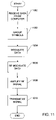
- FIG. 11 shows a flow diagram depicting an exemplary transmission portion of one exemplary embodiment of the present invention.
- FIG. 12 shows a flow diagram depicting an exemplary encoding of data bits according to one exemplary embodiment of the present invention
- FIG. 13 shows a flow diagram depicting an exemplary receiving portion of one exemplary embodiment of the present invention.
- FIG. 14 shows a flow diagram depicting one exemplary approach to decoding data bits according to the principles of the present invention.
- FIG. 2 depicts a wireless local area network 100 according to the present invention.
- a transmitter 102 provides the data that is to be transmitted across antenna 104 to the receiver 106 .
- the receiver 106 receives the transmitted data via antenna 108 .
- FIG. 3 depicts the transmitter 102 ( FIG. 2 ) according to one embodiment of the present invention.
- a computer interface 200 a symbol grouping module 202 , a data modulator 204 , a radio frequency modulator 206 , a radio frequency signal 208 , a radio frequency amplifier 210 , and an antenna 212 are shown.
- the computer interface 200 provides a stream of binary data which represents information to be modulated and transmitted across the wireless local area network 100 ( FIG. 2 ).
- the symbol grouping module 202 receives the stream of binary data from the computer interface 200 and divides the stream into a series of data words, with each data word representing a symbol value.
- the symbol values or data words from the grouping module 202 are then passed to the data modulator 204 .
- the data modulator 204 modulates the data words into CCK modulated data that is compliant with the IEEE802.11b specifications.
- the CCK modulated data is then directed to the radio frequency (RF) modulator 206 which converts the CCK modulated data into a radio frequency signal.
- the radio frequency signal 208 is amplified by the radio frequency amplifier 210 such that it may be transmitted by antenna 212 as packets of data 214 (represented by an arrow in FIG. 3 ).
- the packets of data 214 that are transmitted by the antenna 212 contain a preamble 402 , a header 404 , an operating mode indicator 405 , and encoded data 406 .
- the operating mode indicator 405 contained within the header 404 , is an indication of whether the operating mode is DSSS 1 Mbps, DSSS 2 Mbps, CCK 5.5 Mbps or CCK 11 Mbps mode.
- the CCK encoder 500 includes a differential quadrature phase shift key (DQPSK) modulator 502 and a CCK correlator 504 .
- the computer interface 200 ( FIG. 3 ) outputs data bits d 0 -d 3 (in 5.5 Mbps mode) or d 0 -d 7 (in 11 Mbps mode). Regardless of whether the encoder 500 is operating in 5.5 Mbps mode or 11 Mbps mode, d0 and d1 are applied to the DQPSK modulator to encode the phase parameter ⁇ 1 .
- DQPSK is well-known in the art.
- the phase parameter ⁇ 1 is determined based on the data bits d 0 and d 1 according to the table below:
- Phase Phase (d1, d0) (even symbols) (odd symbols) 00 0 B 01 B/2 ⁇ B/2 10 ⁇ B/2 B/2 11 B 0
- Data bits d 2 -d 3 (5.5 Mbps) or d 2 -d 7 (11 Mbps) are applied to the CCK correlator 504 .
- the CCK correlator 504 receives the appropriate data bits (d 2 -d 3 or d 2 -d 7 ) and encodes the phase parameters ⁇ 2 , ⁇ 3 and ⁇ 4 according to equation (2) or equation (3), respectively.
- An even/odd rotator (not shown) may be utilized in the encoder 500 to output a signal that toggles between two different states. For even symbols, no rotation is applied to the phase value. For odd symbols, an additional rotation of B is applied to the phase value. By additionally encoding data with such a signal, effects of DC offset are reduced because any encoded symbol will have been encoded with a different odd/even status from the immediately preceding and following encoded symbols.
- phase parameter values may then be substituted into equation (1) to yield the eight-chip symbol. It should be noted that the symbol will contain eight complex chips, regardless of whether four data bits (5.5 Mbps) or eight data bits (11 Mbps) are used.
- the eight-chip symbol is then RF modulated by RF modulator 206 , amplified by RF amplifier 210 , and transmitted from antenna 212 ( FIG. 3 ).
- ⁇ 2 is equal to (d2*2+1)*B/2 or (0*2+1)*B/2 which equals B/2.
- ⁇ 3 is defined as 0 in 5.5 Mbps mode.
- ⁇ 4 is equal to d3*2*B/2 or B.
- FIG. 6 illustrates one exemplary embodiment of a receiver 600 (receiver 106 in FIG. 2 ) in accordance with the principles of the present invention.
- the receiver 600 includes an antenna 602 , an RF amplifier 604 , an RF demodulator 606 , a data demodulator 608 , and a computer interface 610 .
- the encoded data packets transmitted by the antenna 212 ( FIG. 3 ) are received by the antenna 602 .
- the encoded data packets are applied to the RF amplifier 604 and the RF demodulator 606 to restore the data packets to a baseband signal.
- the data packets are then demodulated by the data demodulator 608 so that the original data from the computer interface 200 may be recovered.
- the data demodulator 608 includes a CCK 64-vector correlator 702 and a DQPSK demodulator 704 .
- the CCK 64-vector correlation implemented by the illustrated CCK correlator 702 can be written as:
- the correlator output R may be expanded as shown below:
- FIG. 8 A single-vector implementation of the CCK correlator described above is depicted in FIG. 8 . It should be appreciated that because the correlator 800 depicted in FIG. 8 is a single-vector correlator, application of a particular combination of phase parameters ⁇ 2 , ⁇ 3 and ⁇ 4 to the correlator 800 will yield a single output value R of the set of 64 possible correlator outputs values 802 .
- FIG. 9 One exemplary embodiment of the 64-vector CCK correlator 702 according to the present invention is depicted in FIG. 9 .
- the received symbol c made up of chips c 0 -c 7 , is applied to the input of the correlator 702 .
- ⁇ 3 Rotator 710 is provided to rotate or cycle through the four possible values that ⁇ 3 may assume.
- ⁇ 3 may only assume four possible values when operating in 11 Mbps mode; in 5.5 Mbps mode, ⁇ 3 is fixed at a value of 0.
- Two terms are summed at summers 712 .
- a ⁇ 3 -rotated value of c0 i.e., c0*e ⁇ j ⁇ 3
- c1 a ⁇ 3 -rotated value of c1 is summed with ⁇ c3, etc.
- the four possible vectors of ⁇ 2 (1, ⁇ j, ⁇ 1, j) are applied to the output of the summers 712 .
- Two terms corresponding to ⁇ 2 and ⁇ 3 that have been decomposed according to equation (5) are summed at summers 716 .
- the four possible vector values of ⁇ 4 are applied to modify the outputs 718 of the summers 716 .
- the correlator 702 When the correlator 702 is operating in 11 Mbps mode, four clock cycles will be required in order to generate the 64 possible outputs 722 , i.e. 16 outputs 722 per clock cycle, with the ⁇ 3 Rotators 710 rotating once per clock cycle.
- the correlator 702 When the correlator 702 is operating in the 5.5 Mbps mode, however, only one clock cycle will be required to generate all available outputs 722 . This is because, in the 5.5 Mbps mode, ⁇ 3 may only assume the value 0, such that there is no need to rotate through other possible vector values.
- the correlator design of the present invention the amount of power required for demodulating while operating at 5.5 Mbps is greatly reduced compared to the prior art correlators as described above. Further, the correlator of the present invention is appreciably faster, because there is no need to rotate through the other possible ⁇ 3 values.
- the correlator outputs 722 are analyzed to determine which of the outputs r 0 -r 15 is of the greatest magnitude. Referring to FIG. 10 , each of the correlator outputs 722 is applied to an absolute value module 750 .
- the absolute value module 750 will output a value representative of the magnitude of the inputted correlator output r 0 - 15 , respectively.
- the maximum value is held in a current maximum value module 754 .
- the value in the current maximum value module 754 is preferably initialized to 0 such that the actual maximum correlator output 722 for the first iteration of phase rotations will be stored.
- the output of each absolute value module 750 and the current maximum value held in the current maximum value module 754 are compared.
- 17 comparisons are performed (one for each of the sixteen correlator outputs and one for the previous maximum value) for each of the four phase rotations of the ⁇ 3 rotator. If the correlator 702 is operating in 5.5 Mbps mode, then all of the possible correlator values will have been generated, and the maximum value of those output values will be known and stored in the current maximum value module 754 . If the correlator 702 is operating in 11 Mbps mode, then ⁇ 3 will be rotated three times, spanning all four phase values, and the correlator 702 will generate 16 correlator output values with each rotation.
- the index of the CCK correlator 702 with a maximum value is mapped to the corresponding data values.
- the original data values d 2 -d 7 (11 Mbps) or d 2 - 3 (5.5 Mbps) are determined through the use of an encoder, e.g. look-up table 758 .
- Look-up table 758 outputs data bits that correspond to the correlator index that has the maximum correlator output value.
- the maximum correlator output value is also used to determine data values d 0 -d 1 . This is done through DQPSK demodulation performed by DQPSK demodulation module 704 ( FIG. 7 ).
- the original data values d 0 -d 3 (5.5 Mbps) or d 0 -d 7 (11 Mbps) are then provided by the data demodulator 608 to the computer interface 610 ( FIG. 6 ).
- FIG. 11 is a flow diagram depicting the transmission portion according to one embodiment of the present invention.
- data is received from a computer via the computer interface 200 ( FIG. 3 ).
- the data is then grouped into symbols in block 1002 by the symbol grouping module 202 ( FIG. 3 ).
- the data is modulated by the data modulator 204 ( FIG. 3 ).
- the baseband modulated data is then RF modulated in block 1006 by the RF modulator 206 ( FIG. 3 ).
- the RF signal is amplified by RF amplifier 210 ( FIG. 3 ).
- the amplified RF signal is transmitted in block 1010 by antenna 212 ( FIG. 3 ).
- FIG. 12 is a flow diagram depicting the encoding or data modulation portion according to one exemplary embodiment of the present invention.
- data bits d 0 and d 1 are DQPSK encoded by the DQPSK encoder 500 ( FIG. 5 ).
- a determination is then made as to whether the CCK encoder 500 is operating in 5.5 Mbps or 11 Mbps mode (block 1102 .). An indication of the operating mode is stored in the header 404 ( FIG. 4 ). If the CCK encoder 500 is operating in 5.5 Mbps mode, then, in block 1104 , data bits d 2 -d 3 are applied to the CCK correlator 504 ( FIG. 5 ). It should be recognized that four bits are used in 5.5 Mbps encoding. If the CCK encoder 500 is operating in 11 Mbps mode, then, in block 1106 , data bits d 2 -d 7 are applied to the CCK correlator 504 ( FIG. 5 ).
- FIG. 13 is a flow diagram depicting the receiving portion according to one embodiment of the present invention.
- the RF signal transmitted by antenna 212 ( FIG. 3 ) is received by antenna 602 ( FIG. 6 ).
- the RF signal is then amplified at block 1202 by RF amplifier 604 ( FIG. 6 ).
- the amplified RF signal is demodulated by the RF demodulator 606 ( FIG. 6 ).
- the demodulated RF signal is then in block 1206 demodulated by the data demodulator 608 ( FIG. 6 ).
- the demodulated data is then supplied to a receiver computer (not shown) via computer interface 610 ( FIG. 6 ).
- FIG. 14 is a flow diagram depicting data demodulation according to one exemplary embodiment of the present invention.
- the data demodulator 608 FIGS. 6-7
- the ⁇ 3 rotator is set to output a value of 0, as ⁇ 3 is not rotated in 5.5 Mbps mode according to one exemplary embodiment of the present invention.
- the correlator 702 then generates 16 outputs (block 1308 ).
- the correlator 702 keeps only four of the outputs which correspond to the four vectors used for the 5.5 Mbps mode. The other twelve output values are forced to a value of 0 (block 1309 ). If, on the other hand, the data demodulator 608 is operating in 11 Mbps mode, then at block 1306 the received symbol is applied to the correlator 702 ( FIG. 7 ).
- the ⁇ 3 rotator is now set to rotate through its four values (0, B/2, B and 3B/2), so that the correlator 702 will generate 64 outputs (block 1310 ).
- the maximum correlator output is determined.
- the maximum correlator output is then demodulated to output the original data (block 1314 ).
- the demodulation of the block 1314 is performed by DQPSK demodulating the data to determine data bits d 0 and d 1 (block 1316 ) and using a look-up table to recover data bits d 2 -d 3 (5.5 Mbps) or d 2 -d 7 (11 Mbps) (block 1318 ).
Abstract
A method of decoding data includes receiving a symbol and determining a data rate that was used to encode the symbol. A set of correlator output signals are generated based on a first mode when a first data rate was used to encode the symbol and based on a second mode when a second data rate was used to encode the symbol. A maximum-valued signal in one of the set of correlator output signals is identified. The maximum-valued signal in one of the set of correlator output signals is modulated.
Description
This application is a continuation of U.S. patent application Ser. No. 10/092,971, filed Mar. 5, 2002 now U.S. Pat. No. 7,145,969 which claims priority under 35 U.S.C. § 119 (e) of U.S. Provisional Patent Application Ser. No. 60/277,258, filed on Mar. 21, 2001, the contents of each of which are hereby incorporated by reference.
1. Technical Field
This invention relates generally to wireless local area networks, and more particularly, to wireless local area networks employing physical layer modulation and demodulation in accordance with IEEE802.11b.
2. Related Art
There are several known techniques for transmitting digital waveforms across wireless networks. One known technique is direct sequence spread spectrum (DSSS), which allows for high-rate modulation using complementary codes known as “spreading codes.” The use of spreading codes enables the bandwidth occupied by a DSSS waveform to be increased or “spread.” As a consequence of this bandwidth spreading (and despreading), DSSS systems are able to realize processing gains compared to systems using other transmission techniques.
Complementary Code Keying (CCK) is the modulation technique chosen for IEEE 802.11b high rate modes (5.5 Mbps mode and 11 Mbps mode). For example, a CCK modulated symbol c may be expressed as:
c={e j(φ1 +φ 2 +φ 3 +φ 4 ) ,e j(φ 2 +φ 3 +φ 4 ) −,e j(φ 1 +φ 2 +φ 4 ) ,e j(φ 1 +φ 4 ) ,e j(φ 1 +φ 2 +φ 3 ) ,e j(φ 1 +φ 3 ) ,−e j(φ 1 +φ 2 ) ,e jφ 1 } (1)
c={e j(φ
where ν1, ν2, ν3 and ν4 are suitable phase values as described in more detail below.
For clarity of description, the chips in equation (1) are hereinafter referenced from left to right as c0-c7, respectively. In CCK modulation, the 4th and 7th chips, namely c3 and c6, are rotated 180° to optimize the correlation properties and reduce DC offset.
When operating in the 5.5 Mbps CCK mode (4 bits/symbol), the various phase values ν1, ν2, ν3 and ν4 employed in equation (1) are defined as shown below in equation (2).
where d0, d1, d2 and d3 are the 4 bits to be modulated.
When operating in the 11 Mbps CCK mode (8 bits/symbol), the various phase values are defined as shown below in equation (3).
where d0, d1, . . . , d6 and d7 are the 8 bits to be modulated.
When demodulating, the d2-d3 bits (5.5 Mbps mode) or the d2-d7 bits (11 Mbps mode) will be decoded by the CCK correlator, and d0-d1 by DQPSK demodulation.
The published CCK 64-vector correlation can be written as:
where CT=(c0, c1, c2, −c3, c4, c5, −c6, c7) (In-phase and Quadrature signal).
The present invention relates to a method and apparatus for a CCK correlator employing a reduced power consumption and achieves faster performance in the 5.5 Mbps mode of operation as compared with the 11 Mbps mode of operation.
An apparatus and method for decoding CCK-encoded data that has been encoded at one of first and second differing data rates is described. In one embodiment of the present invention, a CCK demodulator receives a symbol, determines based upon an indication contained with the data header whether the symbol was encoded at the first or second data rate, e.g. 5.5 Mbps or 11 Mbps, applies the symbol to a correlator to generate a set of correlator outputs based on the rate at which the symbol was encoded, identifies the maximum-valued correlator output signal, and demodulates the maximum-valued one of the correlator output signals to yield the CCK encoded data. The symbol preferably comprises eight complex chips. Further, the correlator comprises a phase rotator which rotates if the data was modulated at the higher data rate, e.g. 11 Mbps. Still further, the phase rotator is rotated through a predetermined number of phases, wherein the predetermined number is preferably four. The number of correlator output signals is dependent upon whether the data was encoded at the first or second data rate. After determining the maximum-valued correlator output signal, certain data bits are preferably decoded through the use of a look-up table. Some data bits are preferably decoded through the use of a DQPSK demodulator. The demodulator preferably determines if the data was encoded at the first or second data rate, e.g., 5.5 Mbps or 11 Mbps, based on information contained in the header of the encoded data.
An exemplary operating environment for the illustrated system of the present invention is depicted in FIG. 2 . Specifically, FIG. 2 depicts a wireless local area network 100 according to the present invention. A transmitter 102, an antenna 104, a receiver 106 and an antenna 108 are depicted. The transmitter 102 provides the data that is to be transmitted across antenna 104 to the receiver 106. The receiver 106 receives the transmitted data via antenna 108.
Referring to FIG. 4 , the packets of data 214 that are transmitted by the antenna 212 contain a preamble 402, a header 404, an operating mode indicator 405, and encoded data 406. The operating mode indicator 405, contained within the header 404, is an indication of whether the operating mode is DSSS 1 Mbps, DSSS 2 Mbps, CCK 5.5 Mbps or CCK 11 Mbps mode.
Encoding Data
Referring to FIG. 5 , a CCK encoder 500 according to one exemplary embodiment of the present invention is depicted. The CCK encoder 500 includes a differential quadrature phase shift key (DQPSK) modulator 502 and a CCK correlator 504. The computer interface 200 (FIG. 3 ) outputs data bits d0-d3 (in 5.5 Mbps mode) or d0-d7 (in 11 Mbps mode). Regardless of whether the encoder 500 is operating in 5.5 Mbps mode or 11 Mbps mode, d0 and d1 are applied to the DQPSK modulator to encode the phase parameter ν1. DQPSK is well-known in the art. The phase parameter ν1 is determined based on the data bits d0 and d1 according to the table below:
| Phase | Phase | |
| (d1, d0) | (even symbols) | (odd symbols) |
| 00 | 0 | B |
| 01 | B/2 | −B/2 |
| 10 | −B/2 | B/2 |
| 11 | |
0 |
Data bits d2-d3 (5.5 Mbps) or d2-d7 (11 Mbps) are applied to the CCK correlator 504. The CCK correlator 504 receives the appropriate data bits (d2-d3 or d2-d7) and encodes the phase parameters ν2, ν3 and ν4 according to equation (2) or equation (3), respectively.
An even/odd rotator (not shown) may be utilized in the encoder 500 to output a signal that toggles between two different states. For even symbols, no rotation is applied to the phase value. For odd symbols, an additional rotation of B is applied to the phase value. By additionally encoding data with such a signal, effects of DC offset are reduced because any encoded symbol will have been encoded with a different odd/even status from the immediately preceding and following encoded symbols.
After the data bits have been applied to the CCK encoder 500, all of the phase parameters ν1, ν2, ν3 and ν4 will have been encoded. With all of the phase parameters thus being known, the phase parameter values may then be substituted into equation (1) to yield the eight-chip symbol. It should be noted that the symbol will contain eight complex chips, regardless of whether four data bits (5.5 Mbps) or eight data bits (11 Mbps) are used. The eight-chip symbol is then RF modulated by RF modulator 206, amplified by RF amplifier 210, and transmitted from antenna 212 (FIG. 3 ).
Encoding Example
As an example, if the CCK modulator 500 is operating in 5.5 Mbps mode and receives four data bits d3-d0 (MSB to LSB) {1, 0, 0, 1}, the output of the DQPSK modulator 502 will be B/2, and therefore ν1=B/2. ν2 is equal to (d2*2+1)*B/2 or (0*2+1)*B/2 which equals B/2. ν3 is defined as 0 in 5.5 Mbps mode. Finally, ν4 is equal to d3*2*B/2 or B. Thus {ν1, ν2, ν3, ν4} equals {B/2, B/2, 0, B}. Substituting those values into equation (1) yields the symbol c={ej2B, ejB/2, ej2B, —ej3B/2, ejB, ej3B/2, −ejB, ejB/2}. Euler's formula is provided below in equation (4):
e jθ=cos θ+j sin θ (4)
e jθ=cos θ+j sin θ (4)
Substituting the complex chip values for c (shown above) into equation (4) yields the complex symbol c={1, −j, 1, j, −1, −j, 1, j}. Thus it is apparent that any symbol to be transmitted may be derived through the use of the above equations.
Decoding Data
Referring to FIG. 7 , one exemplary embodiment of the data demodulator 608 (FIG. 6 ) is shown in further detail. The data demodulator 608 includes a CCK 64-vector correlator 702 and a DQPSK demodulator 704. The CCK 64-vector correlation implemented by the illustrated CCK correlator 702 can be written as:
The correlator output R may be expanded as shown below:
A single-vector implementation of the CCK correlator described above is depicted in FIG. 8 . It should be appreciated that because the correlator 800 depicted in FIG. 8 is a single-vector correlator, application of a particular combination of phase parameters ν2, ν3 and ν4 to the correlator 800 will yield a single output value R of the set of 64 possible correlator outputs values 802.
One exemplary embodiment of the 64-vector CCK correlator 702 according to the present invention is depicted in FIG. 9 . The received symbol c, made up of chips c0-c7, is applied to the input of the correlator 702. It should be appreciated that, through the use of four different vector values for each of the phase parameters ν2, ν3 and ν4, 64 different correlator output values are possible (4*4*4=64). ν3 Rotator 710 is provided to rotate or cycle through the four possible values that ν3 may assume. Of course, it should be appreciated that ν3 may only assume four possible values when operating in 11 Mbps mode; in 5.5 Mbps mode, ν3 is fixed at a value of 0. Two terms are summed at summers 712. For example, a ν3-rotated value of c0 (i.e., c0*e^jν3) is summed with c2, a ν3-rotated value of c1 is summed with −c3, etc. At 714, the four possible vectors of ν2 (1, −j, −1, j) are applied to the output of the summers 712. Two terms corresponding to ν2 and ν3 that have been decomposed according to equation (5) are summed at summers 716. At 718, the four possible vector values of ν4 are applied to modify the outputs 718 of the summers 716. Finally, two terms corresponding to ν2, ν3 and ν4 that have been decomposed according to equation (5) are summed at summers 720. The output of the various summers 720 correspond to correlator outputs r0-r15 (i.e. outputs 722). Thus, for any given value of ν3, there will be sixteen possible correlator outputs 722 with an index [ν2, ν4].
When the correlator 702 is operating in 11 Mbps mode, four clock cycles will be required in order to generate the 64 possible outputs 722, i.e. 16 outputs 722 per clock cycle, with the ν3 Rotators 710 rotating once per clock cycle. When the correlator 702 is operating in the 5.5 Mbps mode, however, only one clock cycle will be required to generate all available outputs 722. This is because, in the 5.5 Mbps mode, ν3 may only assume the value 0, such that there is no need to rotate through other possible vector values. As a consequence of the correlator design of the present invention, the amount of power required for demodulating while operating at 5.5 Mbps is greatly reduced compared to the prior art correlators as described above. Further, the correlator of the present invention is appreciably faster, because there is no need to rotate through the other possible ν3 values.
The correlator outputs 722 are analyzed to determine which of the outputs r0-r15 is of the greatest magnitude. Referring to FIG. 10 , each of the correlator outputs 722 is applied to an absolute value module 750. The absolute value module 750 will output a value representative of the magnitude of the inputted correlator output r0-15, respectively. The maximum value is held in a current maximum value module 754. The value in the current maximum value module 754 is preferably initialized to 0 such that the actual maximum correlator output 722 for the first iteration of phase rotations will be stored. The output of each absolute value module 750 and the current maximum value held in the current maximum value module 754 are compared. Thus, in one exemplary embodiment, 17 comparisons are performed (one for each of the sixteen correlator outputs and one for the previous maximum value) for each of the four phase rotations of the ν3 rotator. If the correlator 702 is operating in 5.5 Mbps mode, then all of the possible correlator values will have been generated, and the maximum value of those output values will be known and stored in the current maximum value module 754. If the correlator 702 is operating in 11 Mbps mode, then ν3 will be rotated three times, spanning all four phase values, and the correlator 702 will generate 16 correlator output values with each rotation. Comparisons are performed for each of the rotations and the maximum value of those 64 correlator values will be stored in the current maximum value module 754. It should be appreciated by those skilled in the art that there are numerous other methods of determining the maximum value of a set of output values.
After determining the value of the maximum correlator output 722, the index of the CCK correlator 702 with a maximum value is mapped to the corresponding data values. Specifically, the original data values d2-d7 (11 Mbps) or d2-3 (5.5 Mbps) are determined through the use of an encoder, e.g. look-up table 758. Look-up table 758 outputs data bits that correspond to the correlator index that has the maximum correlator output value.
The maximum correlator output value is also used to determine data values d0-d1. This is done through DQPSK demodulation performed by DQPSK demodulation module 704 (FIG. 7 ).
The original data values d0-d3 (5.5 Mbps) or d0-d7 (11 Mbps) are then provided by the data demodulator 608 to the computer interface 610 (FIG. 6 ).
It should also be appreciated by those skilled in the art that the present invention may be practiced through the use of a general purpose processor, best embodied by software.
While the present invention has been described with respect to what is presently considered to be the preferred embodiment, i.e. a method and apparatus for complementary code keying, it is to be understood that the invention is not limited to the disclosed embodiment. To the contrary, the invention is intended to cover various modifications and equivalent arrangements included within the spirit and scope of the appended claims. For example, it is to be understood that the invention is applicable to other correlator architectures in which phase rotators may selectively be used. The scope of the following claims is to be accorded the broadest interpretation so as to encompass all such modifications and equivalent structures and functions.
Claims (21)
1. A method of decoding data comprising:
receiving a symbol;
determining a data rate that was used to encode the symbol;
generating a set of correlator output signals based on a first mode when a first data rate was used to encode the symbol and based on a second mode when a second data rate was used to encode the symbol;
identifying a maximum-valued signal in one of the set of correlator output signals; and
demodulating the maximum-valued signal in one of the set of correlator output signals.
2. The method of claim 1 , wherein the symbol comprises eight complex chips.
3. The method of claim 1 , further comprising rotating a phase of the symbol to generate the set of correlator output signals if the higher of the first and second data rates was used to encode the symbol.
4. The method of claim 3 , further comprising rotating a phase of the symbol to each of a predetermined number of phases.
5. The method of claim 4 , wherein the predetermined number of phases is four.
6. The method of claim 1 , wherein the set of correlator output signals includes a number of signals that is based on the data rate used to encode the symbol.
7. The method of claim 1 , wherein demodulating the maximum-valued signal in one of the set of correlator output signals includes applying the maximum-valued one of the set of correlator output signals to a look-up table.
8. The method of claim 1 , wherein demodulating the maximum-valued one of the set of correlator output signals includes applying the maximum valued signal in one of the set of correlator output signals to a differential Quadrature Phase Shift Key (QPSK) demodulator.
9. The method of claim 1 , wherein the encoded data includes an indication of a data rate used to encode the symbol, and wherein determining which of the first and second data rates was used to encode the symbol comprises extracting the indication from the encoded data.
10. An apparatus for decoding data comprising:
means for receiving a symbol;
means for determining a data rate that was used to encode the symbol;
means for generating a set of correlator output signals based on a first mode when a first data rate was used to encode the symbol and based on a second mode when a second data rate was used to encode the symbol;
means for identifying a maximum-valued signal in one of the set of correlator output signals; and
means for demodulating the maximum-valued signal in one of the set of correlator output signals.
11. The apparatus of claim 10 , wherein the symbol comprises eight complex chips.
12. The apparatus of claim 10 , further comprising a phase rotating means for generating the set of correlator output signals if a higher one of the first and second data rates was used to encode the symbol.
13. The apparatus of claim 12 , wherein said phase rotating means includes means for rotating the phase of the symbol to each of a predetermined number of phases.
14. The apparatus of claim 13 , wherein the predetermined number of phases is four.
15. The apparatus of claim 10 , wherein the set of correlator output signals includes a number of signals that is based upon the data rate used to encode the symbol.
16. The apparatus of claim 10 , wherein the means for demodulating the signal in one of the set of correlator output signals includes means for applying the signal in one of the set of correlator output signals to a look-up table means.
17. The apparatus of claim 10 , wherein the means for demodulating the maximum valued one of the correlator output signals includes means for applying the maximum valued one of the correlator output signals to a differential Quadrature Phase Shift Key (QPSK) demodulating means.
18. The apparatus of claim 10 , wherein the encoded data includes an indication of a data rate used to encode the symbol, and wherein the means for determining the data rate comprises means for extracting the indication from the encoded data.
19. An apparatus for decoding data encoded at one of first and second differing rates, comprising:
a Complementary Code Keying (CCK) correlator that includes:
a phase rotator; and
a control module that selectively rotates a phase of a symbol using the phase rotator when the data has been encoded at a higher one of first and second differing rates and that does not rotate the phase when the data has been encoded at a lower one of the first and second differing rates.
20. An apparatus for Complementary Code Keying (CCK)-encoding and decoding data at one of first and second differing rates comprising:
a differential Quadrature Phase Shift Key (QPSK) modulator;
a first CCK correlator that receives data to be encoded;
a second CCK correlator that receives data to be decoded and that includes:
a maximum-value module;
a comparator that receives an output of the maximum-value module; and
a phase rotator that selectively rotate phase when the data has been encoded at a higher one of the first and second differing rates; and
a differential Quadrature Phase Shift Key (QPSK) demodulator.
21. The apparatus of claim 20 further comprising:
a first antenna;
a radio-frequency modulator coupled to the differential QPSK modulator and the first antenna;
a second antenna; and
a radio-frequency demodulator that communicates with the second antenna and the differential Quadrature Phase Shift Key (QPSK) demodulator.
Priority Applications (1)
| Application Number | Priority Date | Filing Date | Title |
|---|---|---|---|
| US11/525,327 US7272198B1 (en) | 2001-03-21 | 2006-09-22 | Method and apparatus for complementary code keying |
Applications Claiming Priority (3)
| Application Number | Priority Date | Filing Date | Title |
|---|---|---|---|
| US27725801P | 2001-03-21 | 2001-03-21 | |
| US10/092,971 US7145969B1 (en) | 2001-03-21 | 2002-03-05 | Method and apparatus for complementary code keying |
| US11/525,327 US7272198B1 (en) | 2001-03-21 | 2006-09-22 | Method and apparatus for complementary code keying |
Related Parent Applications (1)
| Application Number | Title | Priority Date | Filing Date |
|---|---|---|---|
| US10/092,971 Continuation US7145969B1 (en) | 2001-03-21 | 2002-03-05 | Method and apparatus for complementary code keying |
Publications (1)
| Publication Number | Publication Date |
|---|---|
| US7272198B1 true US7272198B1 (en) | 2007-09-18 |
Family
ID=37480677
Family Applications (2)
| Application Number | Title | Priority Date | Filing Date |
|---|---|---|---|
| US10/092,971 Expired - Fee Related US7145969B1 (en) | 2001-03-21 | 2002-03-05 | Method and apparatus for complementary code keying |
| US11/525,327 Expired - Lifetime US7272198B1 (en) | 2001-03-21 | 2006-09-22 | Method and apparatus for complementary code keying |
Family Applications Before (1)
| Application Number | Title | Priority Date | Filing Date |
|---|---|---|---|
| US10/092,971 Expired - Fee Related US7145969B1 (en) | 2001-03-21 | 2002-03-05 | Method and apparatus for complementary code keying |
Country Status (1)
| Country | Link |
|---|---|
| US (2) | US7145969B1 (en) |
Cited By (1)
| Publication number | Priority date | Publication date | Assignee | Title |
|---|---|---|---|---|
| US7701871B1 (en) | 2001-11-29 | 2010-04-20 | Marvell International Ltd. | Method and apparatus for determining signal quality |
Families Citing this family (4)
| Publication number | Priority date | Publication date | Assignee | Title |
|---|---|---|---|---|
| US7266359B2 (en) * | 2003-03-18 | 2007-09-04 | Freescale Semiconductor, Inc. | DC interference removal in wireless communications |
| JP3751600B2 (en) * | 2003-03-27 | 2006-03-01 | 株式会社東芝 | Receiving apparatus and receiving method |
| US7817708B2 (en) * | 2007-12-14 | 2010-10-19 | Sivaswamy Associates, Llc. | Orthogonal code division multiplex CCK (OCDM-CCK) method and apparatus for high data rate wireless LAN |
| US9294321B2 (en) * | 2010-05-14 | 2016-03-22 | The Boeing Company | Bit signal structure for differentially encoded broadcasts |
Citations (21)
| Publication number | Priority date | Publication date | Assignee | Title |
|---|---|---|---|---|
| US5579345A (en) * | 1994-10-13 | 1996-11-26 | Westinghouse Electric Corporation | Carrier tracking loop for QPSK demodulator |
| US5615230A (en) | 1994-03-01 | 1997-03-25 | Ascom Tech Ag | Process for transmitting digital signals which combines advantages of OQPSK and π/4-QPSK |
| US5636247A (en) | 1994-09-14 | 1997-06-03 | Lucent Technologies Inc. | Information transmission system |
| US5719867A (en) * | 1995-06-30 | 1998-02-17 | Scientific-Atlanta, Inc. | Plural telephony channel baseband signal demodulator for a broadband communications system |
| US5768323A (en) * | 1994-10-13 | 1998-06-16 | Westinghouse Electric Corporation | Symbol synchronizer using modified early/punctual/late gate technique |
| US5841813A (en) | 1996-09-04 | 1998-11-24 | Lucent Technologies Inc. | Digital communications system using complementary codes and amplitude modulation |
| US5841816A (en) * | 1992-10-22 | 1998-11-24 | Ericsson Inc. | Diversity Pi/4-DQPSK demodulation |
| US5862182A (en) | 1996-07-30 | 1999-01-19 | Lucent Technologies Inc. | OFDM digital communications system using complementary codes |
| US5878085A (en) | 1997-08-15 | 1999-03-02 | Sicom, Inc. | Trellis coded modulation communications using pilot bits to resolve phase ambiguities |
| US5966055A (en) | 1997-02-14 | 1999-10-12 | Lucent Technologies, Inc. | Phase-shift modulation of a direct antenna-driving VCO |
| US6005840A (en) | 1997-04-01 | 1999-12-21 | Lucent Technologies Inc. | Complementary encoding and modulation system for use in an orthogonal frequency division multiplexing transmitter system and method thereof |
| US6233273B1 (en) * | 1999-06-29 | 2001-05-15 | Intersil Americas Inc. | Rake receiver with embedded decision feedback equalizer |
| US20010034254A1 (en) * | 2000-03-24 | 2001-10-25 | Ranta Jukka T. | Power saving in mobile stations |
| US6330273B1 (en) | 1996-03-28 | 2001-12-11 | Roke Manor Research Limited | Apparatus for code tracking in a direct sequence spread spectrum receiver |
| US6345073B1 (en) | 1998-10-08 | 2002-02-05 | The Aerospace Corporation | Convolutional despreading method for rapid code phase determination of chipping codes of spread spectrum systems |
| US6345067B1 (en) | 1997-09-22 | 2002-02-05 | Sharp Kabushiki Kaisha | Clock regenerating circuit in direct spread spectrum communication system |
| US6347112B1 (en) | 1997-10-22 | 2002-02-12 | Commissariat A L'energie Atomique | Circuit for direct sequence spread spectrum digital transmissions with generation of an interference signal |
| US6363104B1 (en) | 1998-10-02 | 2002-03-26 | Ericsson Inc. | Method and apparatus for interference cancellation in a rake receiver |
| US20030012267A1 (en) * | 2000-03-06 | 2003-01-16 | Daisuke Jitsukawa | CDMA receiver, and searcher in a CDMA receiver |
| US20030067904A1 (en) * | 1996-12-20 | 2003-04-10 | Kazuo Nagatani | Code multiplexing transmitting apparatus |
| US6697350B2 (en) * | 1995-06-30 | 2004-02-24 | Interdigital Technology Corporation | Adaptive vector correlator for spread-spectrum communications |
-
2002
- 2002-03-05 US US10/092,971 patent/US7145969B1/en not_active Expired - Fee Related
-
2006
- 2006-09-22 US US11/525,327 patent/US7272198B1/en not_active Expired - Lifetime
Patent Citations (21)
| Publication number | Priority date | Publication date | Assignee | Title |
|---|---|---|---|---|
| US5841816A (en) * | 1992-10-22 | 1998-11-24 | Ericsson Inc. | Diversity Pi/4-DQPSK demodulation |
| US5615230A (en) | 1994-03-01 | 1997-03-25 | Ascom Tech Ag | Process for transmitting digital signals which combines advantages of OQPSK and π/4-QPSK |
| US5636247A (en) | 1994-09-14 | 1997-06-03 | Lucent Technologies Inc. | Information transmission system |
| US5768323A (en) * | 1994-10-13 | 1998-06-16 | Westinghouse Electric Corporation | Symbol synchronizer using modified early/punctual/late gate technique |
| US5579345A (en) * | 1994-10-13 | 1996-11-26 | Westinghouse Electric Corporation | Carrier tracking loop for QPSK demodulator |
| US5719867A (en) * | 1995-06-30 | 1998-02-17 | Scientific-Atlanta, Inc. | Plural telephony channel baseband signal demodulator for a broadband communications system |
| US6697350B2 (en) * | 1995-06-30 | 2004-02-24 | Interdigital Technology Corporation | Adaptive vector correlator for spread-spectrum communications |
| US6330273B1 (en) | 1996-03-28 | 2001-12-11 | Roke Manor Research Limited | Apparatus for code tracking in a direct sequence spread spectrum receiver |
| US5862182A (en) | 1996-07-30 | 1999-01-19 | Lucent Technologies Inc. | OFDM digital communications system using complementary codes |
| US5841813A (en) | 1996-09-04 | 1998-11-24 | Lucent Technologies Inc. | Digital communications system using complementary codes and amplitude modulation |
| US20030067904A1 (en) * | 1996-12-20 | 2003-04-10 | Kazuo Nagatani | Code multiplexing transmitting apparatus |
| US5966055A (en) | 1997-02-14 | 1999-10-12 | Lucent Technologies, Inc. | Phase-shift modulation of a direct antenna-driving VCO |
| US6005840A (en) | 1997-04-01 | 1999-12-21 | Lucent Technologies Inc. | Complementary encoding and modulation system for use in an orthogonal frequency division multiplexing transmitter system and method thereof |
| US5878085A (en) | 1997-08-15 | 1999-03-02 | Sicom, Inc. | Trellis coded modulation communications using pilot bits to resolve phase ambiguities |
| US6345067B1 (en) | 1997-09-22 | 2002-02-05 | Sharp Kabushiki Kaisha | Clock regenerating circuit in direct spread spectrum communication system |
| US6347112B1 (en) | 1997-10-22 | 2002-02-12 | Commissariat A L'energie Atomique | Circuit for direct sequence spread spectrum digital transmissions with generation of an interference signal |
| US6363104B1 (en) | 1998-10-02 | 2002-03-26 | Ericsson Inc. | Method and apparatus for interference cancellation in a rake receiver |
| US6345073B1 (en) | 1998-10-08 | 2002-02-05 | The Aerospace Corporation | Convolutional despreading method for rapid code phase determination of chipping codes of spread spectrum systems |
| US6233273B1 (en) * | 1999-06-29 | 2001-05-15 | Intersil Americas Inc. | Rake receiver with embedded decision feedback equalizer |
| US20030012267A1 (en) * | 2000-03-06 | 2003-01-16 | Daisuke Jitsukawa | CDMA receiver, and searcher in a CDMA receiver |
| US20010034254A1 (en) * | 2000-03-24 | 2001-10-25 | Ranta Jukka T. | Power saving in mobile stations |
Non-Patent Citations (7)
| Title |
|---|
| Bob Pearson, "Complementary Code Keying Made Simple," Intersil, Application Note Nov. 2001 AN9850. |
| Carl Andren, Mark Webster, "CCK Modulation Delivers 11Mbps for High Rate IEEE 802.11 Extension," Wireless Symposium/Portable by Design Conference Spring 1999. |
| IEEE Std 802.11b-1999, The Institute of Electrical and Electronics Engineers, Inc. New York, 2000. |
| Marcel J. E. Golay, "Complementary Series," IRE Transactions on Information Theory April. |
| R. Sivaswamy, "Multiphase Complementary Codes," IEEE Transactions on Information Theory, vol. 24, No. 5, Sep. 1978. |
| Robert L. Frank, "Polyphase Complementary Codes," IEEE Transactions on Information Theory, vol. 26, Nov. 1980. |
| TA Wilkinson, AE Jones, "Minimization of the Peak to Mean Envelope Power Ratio of Multicarrier Transmission Schemes By Block Coding," VTC Chigago, Jul. 1995, 1995 IEEE. |
Cited By (1)
| Publication number | Priority date | Publication date | Assignee | Title |
|---|---|---|---|---|
| US7701871B1 (en) | 2001-11-29 | 2010-04-20 | Marvell International Ltd. | Method and apparatus for determining signal quality |
Also Published As
| Publication number | Publication date |
|---|---|
| US7145969B1 (en) | 2006-12-05 |
Similar Documents
| Publication | Publication Date | Title |
|---|---|---|
| US6865236B1 (en) | Apparatus, and associated method, for coding and decoding multi-dimensional biorthogonal codes | |
| JP3424183B2 (en) | Receiver for direct spread spectrum | |
| JP4527702B2 (en) | Information bit modulation method, digital modulation system, digital demodulation system | |
| JP3778969B2 (en) | Method and apparatus for spread spectrum code pulse position modulation | |
| JP4203551B2 (en) | High data rate spread spectrum transceiver and related methods | |
| US6233271B1 (en) | Method and apparatus for decoding trellis coded direct sequence spread spectrum communication signals | |
| US6356748B1 (en) | Spectrum control for direct conversion radio frequency reception | |
| US6882692B2 (en) | Fast transform system for an extended data rate WLAN system | |
| JPH07170210A (en) | Spread spectrum modulating/demodulating method and modem using the same | |
| US6208615B1 (en) | Broadband wireless access based on code division parallel access | |
| US7272198B1 (en) | Method and apparatus for complementary code keying | |
| US20090154333A1 (en) | Orthogonal code division multiplex cck (ocdm-cck) method and apparatus for high data rate wireless lan | |
| US7787827B2 (en) | Preamble detection | |
| US6125136A (en) | Method and apparatus for demodulating trellis coded direct sequence spread spectrum communication signals | |
| US7602864B1 (en) | Method and apparatus for predicting CCK subsymbols | |
| US6215813B1 (en) | Method and apparatus for encoding trellis coded direct sequence spread spectrum communication signals | |
| US7529305B1 (en) | Combination of space-time coding and spatial multiplexing, and the use of orthogonal transformation in space-time coding | |
| US7957493B2 (en) | Candidate generation | |
| US7177362B2 (en) | Apparatus for adaptive resolution of phase ambiguity value | |
| US6072785A (en) | Differential PSK signalling in CDMA networks | |
| US20080309526A1 (en) | Method and apparatus for a simplified maximum likelihood demodulator for dual carrier modulation | |
| JP2655107B2 (en) | Spread spectrum receiver | |
| CN107317777B (en) | Method for dividing observation space in BPSK demodulation process | |
| US5724382A (en) | Multimode spread spectrum communication system tolerant to varying channel characteristics | |
| US6999533B2 (en) | Demodulating encoded data |
Legal Events
| Date | Code | Title | Description |
|---|---|---|---|
| STCF | Information on status: patent grant |
Free format text: PATENTED CASE |
|
| CC | Certificate of correction | ||
| FPAY | Fee payment |
Year of fee payment: 4 |
|
| FPAY | Fee payment |
Year of fee payment: 8 |
|
| MAFP | Maintenance fee payment |
Free format text: PAYMENT OF MAINTENANCE FEE, 12TH YEAR, LARGE ENTITY (ORIGINAL EVENT CODE: M1553); ENTITY STATUS OF PATENT OWNER: LARGE ENTITY Year of fee payment: 12 |
|
| AS | Assignment |
Owner name: NXP USA, INC., TEXAS Free format text: ASSIGNMENT OF ASSIGNORS INTEREST;ASSIGNOR:MARVELL INTERNATIONAL LTD.;REEL/FRAME:051536/0001 Effective date: 20191206 |