US7277983B1 - Method and apparatus for smoothing current transients in a content addressable memory (CAM) device - Google Patents
Method and apparatus for smoothing current transients in a content addressable memory (CAM) device Download PDFInfo
- Publication number
- US7277983B1 US7277983B1 US11/085,399 US8539905A US7277983B1 US 7277983 B1 US7277983 B1 US 7277983B1 US 8539905 A US8539905 A US 8539905A US 7277983 B1 US7277983 B1 US 7277983B1
- Authority
- US
- United States
- Prior art keywords
- cam
- cam blocks
- blocks
- command
- activated
- Prior art date
- Legal status (The legal status is an assumption and is not a legal conclusion. Google has not performed a legal analysis and makes no representation as to the accuracy of the status listed.)
- Expired - Fee Related, expires
Links
Images


Classifications
-
- G—PHYSICS
- G11—INFORMATION STORAGE
- G11C—STATIC STORES
- G11C15/00—Digital stores in which information comprising one or more characteristic parts is written into the store and in which information is read-out by searching for one or more of these characteristic parts, i.e. associative or content-addressed stores
Definitions
- the present invention relates generally to content addressable memory (CAM) devices, and more particularly to the activation of blocks within a CAM device.
- CAM content addressable memory
- CAM Content addressable memory
- ACL search access control lists
- FIB forwarding information bases
- An ACL can include a set of rules (data set) that can limit access (e.g., forwarding of packets) to only those packets having fields falling within a particular range.
- An FIB can include data necessary for forwarding a packet, typically the generation of a “next hop” address in response to a destination address.
- a typical CAM device can store a number of data values in a CAM cell array.
- a compare (i.e., match) operation entries can be compared to a compare data value.
- An entry that matches the compare data value can result in the generation of a match indication.
- search operations can be conducted in response to a system clock, with searches being undertaken every clock cycle.
- CAM devices can draw considerable current as match lines in the CAM cell array are continuously charged and discharged each clock cycle.
- a cold start operation can occur when a CAM device switches from an idle state, in which the various CAM array sections of the device are not operational, to an active state, in which CAM array sections perform various functions, such as a search operation, or the like.
- parasitic inductance of a package containing a CAM device can prevent a fast ramp up of the current, preventing an adequate current supply from being provided when needed by the CAM device.
- FIG. 17A is a block diagram of one approach for reducing overall transient current in a CAM device.
- a CAM device 1700 can be divided into two halves 1702 - 0 and 1702 - 1 , with each half performing a search on opposite edges of a clock signal, and providing results to a synchronizer/priority encoder 1704 .
- one side 1702 - 1 (Panel B) can precharge match lines, while the other side 1702 - 0 (Panel A) evaluates (i.e., compares a search key to data in CAM entries).
- the two sides operate in the opposite fashion.
- FIG. 17B is a timing diagram showing an average current (I) drawn over time.
- I average current drawn over time.
- the present invention can include a method of activating separate blocks of a content addressable memory (CAM) device.
- the method can include sequentially activating an increasingly larger number of CAM blocks until an initial number of CAM blocks is activated. If the initial number of CAM blocks is not equal to a configurable block number, the method can sequentially change the number of activated CAM blocks until the number of active CAM blocks is equal to the configurable block number value.
- CAM content addressable memory
- CAM block operations can be based on a CAM timing signal.
- a method can determine that the CAM timing signal is stable. Such an arrangement can allow dummy activation operations to take place while other portions of the CAM device are still undergoing power-up sequences.
- determining that a CAM timing signal is stable can include determining that a phase locked loop (PLL) circuit is locked with a received clock signal.
- PLL phase locked loop
- such a step can include determining that a CAM clock signal has executed a predetermined number of cycles.
- sequentially activating an increasingly larger number of CAM blocks can include activating one CAM block each cycle of a clock signal until the initial number of CAM blocks is activated.
- a method can further include receiving a command targeted to activate a command number of CAM blocks. If the command number of CAM blocks is less than the configurable block number, an additional number CAM blocks, not targeted by the command, can be activated until the total number of CAM blocks activated is equal to the configurable block number.
- dummy operations can be used to ensure that a same number of CAM blocks is activated in response to commands, and thus can avoid large current changes that can arise from the activation of different numbers of CAM blocks in successive operations.
- the present invention can also include content addressable memory (CAM) device.
- a CAM device can include a plurality of CAM blocks, each comprising a plurality of CAM entries that compare a key value essentially simultaneously to data values stored in the CAM entries.
- the CAM device can also include a control circuit that receives a first control signal and a configurable block number value.
- a control circuit can sequentially activate an increasingly larger number of CAM blocks in response to a first control signal until an initial number of CAM blocks is activated. Further, if an initial number of CAM blocks is not equal to the configurable block number, the control circuit can sequentially change the number of activated CAM blocks until the number of CAM blocks is equal to the configurable block number value.
- a CAM device can reach an initial number of active blocks, with relatively small current rate changes, without necessarily introducing any additional latency.
- a CAM device can further include a register coupled to the control circuit that stores the configurable block number.
- a user of the CAM device can write a configurable block number to such a register, to thereby establish the number of CAM blocks that can be activated.
- a CAM device can further include a timing circuit that activates the first control signal in response to a received clock signal.
- a timing circuit can include a phase locked loop (PLL) circuit that activates the first control signal when the PLL circuit is locked with the received clock signal.
- PLL phase locked loop
- such a timing circuit can include a clock divider/counter. More particularly, the timing circuit can include a divider circuit coupled to a received clock signal, a counter having an input coupled to the output of the divider circuit and an output that provides a count value, and a comparator that compares the count value to a predetermined value. The comparator can activate the first control signal based on a comparison result.
- a control circuit can sequentially activate one CAM block each cycle of CAM clock signal until the initial number of CAM blocks is activated.
- a control circuit can sequentially change a number of activated CAM blocks by one each cycle of a CAM clock signal until the number of CAM blocks is equal to the configurable block number value.
- control circuit can sequentially decrease the number of active CAM blocks until the number of CAM blocks is equal to the configurable block number value.
- control circuit can sequentially increase the number of active CAM blocks until the number of CAM blocks is equal to the configurable block number value.
- the CAM device can further include a command decoder that decodes a received command targeted to activate a command number of CAM blocks. If the command number of CAM blocks is less than the configurable block number value, the control circuit can activate an additional number CAM blocks not targeted by the decoded command until the total number of activated CAM blocks is equal to the configurable block number value.
- the present invention can also include a method of reducing current consumption rate changes in a content addressable memory (CAM).
- the method can include issuing dummy search operations to increasingly larger numbers of CAM blocks within the CAM device until an initial number of CAM blocks is activated. An initial number of CAM blocks can be less than the total number of CAM blocks in the CAM device.
- the method may further include receiving a configurable block number, and incrementally changing the number of issued dummy searches if the configurable block number is different from the initial number of CAM blocks until the number of activated CAM blocks is equal to the configurable block number.
- issuing dummy search operations to increasingly larger numbers of CAM blocks can include increasing the number of dummy searches to the CAM blocks by one in successive time periods.
- incrementally changing the number of issued dummy searches can include, if the initial number of CAM blocks is greater than the configurable block number, decreasing the number of dummy searches by one in successive time periods until the number of activated CAM blocks is equal to the configurable block number. If the initial number of CAM blocks is less than the configurable CAM block number, the method can increase the number of dummy searches by one in successive time periods until the number of activated CAM blocks is equal to the configurable block number.
- a method can also include receiving a command targeted to activate a command number of CAM blocks, and issuing dummy searches to CAM blocks not targeted by the command if the number of CAM blocks targeted by the command is less than the configurable block number to bring the total number of CAM blocks activated in response to the command to the configurable block number.
- a command can include a read operation that accesses data stored in at least one CAM block.
- FIG. 1 is a block schematic diagram of a CAM device according to a first embodiment of the present invention.
- FIG. 2 is a flow diagram showing a method according to a second embodiment of the present invention.
- FIGS. 3A to 3D are plan views and corresponding timing diagrams showing the operation of CAM device according to a third embodiment.
- FIG. 4 shows plan views and corresponding timing diagram showing a conventional CAM device operation.
- FIG. 5 is a block schematic diagram of a CAM device according to a fourth embodiment of the present invention.
- FIG. 6 is a timing diagram showing a power-up operation of the CAM device shown in FIG. 5 .
- FIG. 7 is a timing diagram showing a command execution operation of the CAM device shown in FIG. 5 .
- FIG. 8 is a flow diagram showing a method according to a fifth embodiment of the present invention.
- FIG. 9 is a flow diagram showing a method according to a sixth embodiment of the present invention.
- FIG. 10 is a block schematic diagram of a timing circuit according to one embodiment.
- FIG. 11 is a block schematic diagram of a CAM device according to a seventh embodiment of the present invention.
- FIG. 12 is a block schematic diagram of a CAM device according to an eighth embodiment of the present invention.
- FIG. 13 is a block schematic diagram of a CAM device according to a ninth embodiment of the present invention.
- FIG. 14 is a block schematic diagram of a CAM device according to a tenth embodiment of the present invention.
- FIG. 15 is a block schematic diagram of a CAM device according to an eleventh embodiment of the present invention.
- FIG. 16 is a block schematic diagram of a CAM device according to a twelfth embodiment of the present invention.
- FIG. 17A is a block diagram showing a conventional CAM device.
- FIG. 17B is a graph illustrating current consumption of the conventional CAM device of FIG. 17A .
- the embodiments include a content addressable memory (CAM) device and operating method that can alleviate current transients occurring over multiple operational cycles by activating different portions (e.g., CAM blocks) of the CAM device according to dummy operations (e.g., a dummy search).
- a “dummy” operation can cause the activation of a CAM block, but does not yield any valid operation data.
- an “actual” operation yield valid data from an accessed CAM block (e.g., search data, read data, etc.).
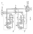
- a CAM device is shown in FIG. 1 , and designated by the general reference character 100 .
- a CAM device 100 can include a number of CAM blocks 102 - 1 to 102 - 16 , a start-up circuit 104 , and a control circuit 106 .
- Each CAM block ( 102 - 1 to 102 - 16 ) can include multiple CAM entries, each of which can compare a search key value to a stored data value.
- a start-up circuit 104 can detect predetermined device states in response to power being applied to a CAM device 100 . According to such states, a start-up circuit 106 can activate an indication received by control circuit 106 . In the very particular example of FIG. 1 , a start-up circuit 104 can determine that internal timing within the CAM is stable, and activate a signal CLK_STAT.
- a control circuit 106 can receive the indication from a start-up circuit 104 about the internal start-up time. Also, control circuit 106 can receive a user block number USER_BLK from a user after an external start-up time. The external start-up time can always be greater than an internal start-up time.
- a user block number USER_BLK can be a configurable value. More particularly, a user block number USER_BLK can be provided by the user of the CAM device 100 to establish a maximum number of blocks that will be in use in the device.
- the number of CAM blocks activated in a given cycle can be maintained at the USER_BLK value, thereby reducing the overall power consumed by the CAM device. This is in contrast to a conventional device that would activate all CAM blocks.
- a control circuit 106 can be connected to CAM blocks ( 102 - 1 to 102 - 16 ) by way of a command bus 108 and a data bus 110 .
- a command bus 108 can carry one or more signals for activating each CAM block. Such signals can be command signals corresponding to particular types of CAM operations, including but not limited to search operations, read operations, write operations, and “learn” operations.
- a command bus 108 can carry “dummy” operation signals that can activate a given CAM block in the same general fashion as an actual operation, but not yield a valid result. As such, a CAM block activated in a dummy operation can draw a similar, if not essentially the same amount of current as a CAM block executing an actual operation of the same type.
- FIGS. 2 and 3A to 3 D Having described the general structure of a CAM device 100 according to a first embodiment, a method according to a second embodiment will now be described with reference to FIGS. 2 and 3A to 3 D.
- FIG. 2 is a flow diagram showing a method 200 according to a second embodiment.
- the embodiment of FIG. 2 can be considered related to that of FIG. 1 in that the CAM device 100 can operate according to the method of FIG. 2 .
- a method 200 can include a start-up (step 202 ), which can include power being applied to a CAM device, or a CAM device being reset, or otherwise reconfigured. Thus, in the embodiment of FIG. 1 , this can include power being applied to CAM device 100 .
- a method can further include determining whether timing has reached a settled state (step 204 ) or the internal clocks are stable in order to perform at least dummy operations. Such a step can include ensuring a device has sufficient functionality to execute at least dummy operations. If timing is not settled (N branch from 204 ), a method can wait until such a state is reached. In the embodiment of FIG. 1 , this can include a start-up circuit 104 determining that timing has settled and activating a CLK_STAT indication.
- a method can proceed to sequentially activate an increasingly larger number of CAM blocks until an initial number of CAM blocks is activated (step 206 ).
- Such a step can include executing dummy operations in sequentially larger numbers of CAM blocks. Even more particularly, such a step can include sequentially increasing the number of CAM blocks activated by one, until half of the total number of CAM blocks is activated.
- a step 206 can include a control circuit 106 issuing dummy commands to increasingly larger numbers of the CAM blocks ( 102 - 1 to 102 - 16 ). As but one example, a control circuit can issue dummy search commands with dummy key values.
- a method 200 can include receiving a second block number value (step 208 ).
- a second block number value can be a configurable value that establishes a limit to the maximum number of CAM blocks allowed to be activated at a time. In one very particular case, such a value can be user programmable value that establishes a maximum number of blocks that will take part in any compare operation.
- a step 208 can include a control circuit 106 receiving and/or reading a USER_BLK value.
- a method 200 can then adjust the number of active CAM blocks in a step-wise fashion until the number of active CAM blocks is equal to the second block number value (step 210 ).
- Such a step can include determining if the initial number of CAM blocks is different than the second block number value. If a difference exists, dummy operations can be increased/decreased in the CAM blocks until the number of active CAM blocks equals the second block number value.
- a step 210 can include sequentially increasing/decreasing the number of CAM blocks activated by one, until the second block number value is reached.
- a step 210 can include a control circuit 106 increasing or decreasing the number of dummy commands issued to the CAM blocks ( 102 - 1 to 102 - 16 ), as needed, to eventually activate the number of CAM blocks indicated by the USER_BLK value.
- CAM blocks can be activated in a sequential fashion in a start-up operation to thereby reduce the size of a current rate change.
- a method 200 can also include command related steps.
- a method can include receiving a command (step 212 ). Such a step can include receiving a command from a CAM user that specifies a particular number of CAM blocks that will be activated. In response to such a command, a method 200 can adjust the number CAM blocks activated in response to the command so that the number of active CAM blocks is equal to the second block number value (step 214 ). Such a step can include issuing dummy commands to non-targeted CAM blocks in addition to actual command targeted to particular CAM blocks.
- FIGS. 3A to 3D are plan view diagrams showing a CAM operation according to a third embodiment.
- Each of FIGS. 3A to 3D shows a CAM device having 16 CAM blocks, each represented by a square, with the dummy activation of a CAM block being indicated by hatching.
- Each of the figures also shows a representation of a resulting current consumption rate (dl/dt) as compared to a conventional approach.
- the embodiment of FIGS. 3A to 3D can be considered related to that of FIGS. 1 and 2 in that operations shown can correspond to portions of the method set forth in FIG. 2 .
- FIG. 3A a start up activation sequence is shown going from left to right.
- a CAM block 300 - 1 can be activated.
- CAM block 300 - 2 in a sequential fashion until CAM block 300 - 8 is activated, for a total of eight CAM blocks.
- the sequence illustrated in FIG. 3A can be considered related to FIG. 2 in that it can correspond to steps 202 to 206 of FIG. 2 .
- each individual CAM block can result in an increase in the rate at which current is drawn.
- rate can be small (e.g., 1/16 th ) as compared to a conventional arrangement, shown by a dashed line, that would activate 16 CAM blocks essentially simultaneously.
- a CAM block 302 - 1 can be activated, followed by a CAM block 302 - 2 .
- Inactive CAM blocks can be activated by dummy operations in this fashion until 14 CAM blocks are activated.
- the activation of each individual CAM block result in the same relatively small rate increases as shown in FIG. 3A . This rate can be small as compared to an abrupt activation of CAM blocks that could occur in a conventional approach, shown by a dashed line, in which an additional 6 CAM blocks are activated essentially simultaneously.
- a second example of an adjustment sequence is shown going from left to right.
- a CAM block 304 - 1 can be deactivated, followed by a CAM block 3042 being deactivated.
- the de-activation of each individual CAM block can result in a sequence of relatively small rate decreases, as opposed a higher current rate change that would result when multiple CAM blocks are deactivated simultaneously.
- sequence illustrated in FIGS. 3B and 3C can be considered related to FIG. 2 in that such sequences can correspond to step 210 of FIG. 2 .
- a command adjustment sequence is shown going from left to right.
- the sequence shows a CAM device with 14 CAM blocks being activated by dummy operations that receives a first command targeted at eight CAM blocks followed by a second command targeted at six CAM blocks.
- CAM blocks activated in response to a command are shown with the symbol “C”.
- C CAM blocks activated in response to a command
- a number of additional CAM blocks are activated with dummy operations in order to ensure that the number of CAM blocks is maintained at 14, regardless of the number of CAM blocks that are targeted by a command.
- current rate changes can be kept at a minimum.
- FIG. 3D is in contrast to a conventional approach shown in FIG. 4 , that would activate different numbers of CAM blocks in response to each different command, thus generating considerable dl/dt changes.
- the sequence illustrated in FIG. 3D can be considered related to FIG. 2 in that such a sequence can correspond to steps 212 and 214 of FIG. 2 .
- a CAM device according to a fourth embodiment is shown in FIG. 5 , and designated by the general reference character 500 .
- a CAM device 500 can include some of the same general sections as FIG. 1 , thus like sections are referred to by the same reference character but with the first digit being a “5” instead of a “1”. Further, a CAM device according to a fourth embodiment can be considered related to that of the first embodiment in that it can represent a more detailed example of a first embodiment.
- CAM blocks ( 502 - 1 to 502 - 16 ) can receive an internal clock signal CLK, and base the timing of operations on such a signal.
- a start-up circuit 504 can include a phase locked loop (PLL) circuit 504 - 0 and a power-up circuit 504 - 1 .
- a PLL circuit 504 - 0 can receive an external clock signal CLK_EX and generate an internal clock signal CLK that tracks (i.e., that is locked with) external clock signal CLK_EX.
- a PLL circuit 5040 can activate a status signal CLK_STAT provided to control circuit 506 .
- a power-up circuit 504 - 1 can determine when a CAM device 500 is fully operational after the application of power. It is noted that a PLL circuit 504 - 0 may activate status signal 506 prior to power-up circuit 504 - 1 indicating the CAM device 500 is fully operational.
- a control circuit 506 can include control logic 506 - 0 , at least one user register 506 - 1 , and a command decoder 506 - 2 .
- Control logic 506 - 0 can issue commands, including dummy commands, on a command bus 508 in response to command data received on external bus 506 - 3 and decoded by command decoder 506 - 2 and/or a status value CLK_STAT.
- control logic 506 - 0 can receive and parse data received on bus 506 - 3 , and output such data (e.g., search key values) on data bus 510 .
- a user register 506 - 1 can be one of a plurality of addressable registers for receiving and storing configurable values.
- a user register 506 - 1 can store a user block number value USER_BLK that can represent the maximum number of blocks enabled during a compare operation by a user.
- a command decoder 506 - 2 can decode received command data.
- a command decoder 506 - 2 can generate a command block value CMD_BLK, that can represent the number of CAM blocks ( 502 - 1 to 502 - 16 ) targeted by a given command.
- FIG. 6 is a timing diagram showing the sequential activation of CAM blocks with dummy operations in response to a power-up event.
- FIG. 6 includes a waveform of an external clock CLK_EX, an internal clock output by a PLL circuit CLK, a status indication CLK_STAT, a power-up indication PWR_UP, the status of various CAM blocks CAM BLK 1 to CAM BLK 16 , and a user block status USER_BLK.
- CAM device 500 Prior to time t 1 , power and an external clock CLK_EX can be applied to a CAM device 500 .
- a PLL circuit 5040 can begin trying to lock onto external clock signal CLK_EX. Because it may take some clock cycles for lock to take place, a status indication CLK_STAT can indicate that the PLL circuit 504 - 0 is not yet locked (remain low in this example). All CAM blocks ( 502 - 1 to 502 - 16 ) can be inactive at this time.
- a PLL circuit 504 - 0 can achieve a locked state with external clock signal CLK_EX and can activate status indication CLK_STAT (drive the signal high in this example).
- FIG. 6 shows the clock signal CLK in phase with external clock signal, such a signal could be phase shifted with respect to (but still synchronous with) an external clock signal CLK_EX.
- an internal clock could be a multiplied and/or divided version of an external clock.
- control logic 506 - 0 can begin sequentially activating increasingly larger numbers of CAM blocks, with dummy operations, until an initial number of CAM blocks are being activated every cycle.
- control logic 506 - 0 activates an additional CAM block each cycle, until an initial eight CAM blocks are activated. Dummy activation of a CAM block is represented by the symbol “DUM”.
- a power-up circuit 504 - 1 can activate a power up indication PWR_UP to indicate that a CAM device has successfully completed a power-up sequence.
- a user block number value can be valid.
- the value can be read from a user register 506 - 1 to control logic.
- an indication can be generated to notify users that a user register 506 - 1 can now store a user block number value.
- control logic 506 - 0 can sequentially activate or deactivate CAM blocks with dummy operations until the number of active CAM blocks is equal to the user block value.
- the user block number is ten, thus control logic 506 - 0 activates CAM blocks 1 - 9 (by enabling CAM block 9 ) in one cycle, and then CAM blocks 1 - 10 in the next cycle.
- a CAM device upon power-up, can activate a sequential numbers of CAM blocks to meet some initial number, and then, if necessary, sequentially adjust such a number to meet a user configurable (visible) number of active CAM blocks.
- FIG. 7 is a timing diagram showing the activation of CAM blocks in response to various command that target a specific number of CAM blocks.
- FIG. 7 includes most of the waveforms shown in FIG. 6 , but also adds a command waveform CMD, which shows a received command.
- a CAM device 500 can be continuing to activate a configurable number of CAM blocks (in this example ten) by way of dummy operations.
- a first search command can be received.
- a first search command (SRCH A) can direct searches to be performed on all or a portion of the user “visible” CAM blocks.
- SEARCH A is directed to CAM blocks 1 - 8 .
- block searches can be executed on CAM blocks 1 - 8 .
- dummy searches can be executed on CAM blocks 9 and 10 in order to maintain the number of activated blocks at the configurable number (in this case 10 ).
- a second search command (SRCH B) is received.
- SRCH B is directed to CAM blocks 1 - 10 .
- block searches can be executed on CAM blocks 1 - 10 . No dummy searches are issued, as the number of CAM blocks searched is equal to the configurable number.
- a read command (READ) is received.
- READ read command
- FIG. 7 it is assumed that the READ command is directed to CAM block 8 .
- control logic can issue dummy reads to CAM blocks 1 - 7 and 9 - 10 in order to continue to maintain the number of CAM blocks activated at the user configurable number.
- the CAM device can continue to activate the same number of CAM block even if a received command is directed to a smaller number of CAM blocks.
- FIG. 8 a fifth embodiment of the present invention is set forth in a flow diagram and designated by the general reference character 800 .
- the embodiment of FIG. 8 can be considered related to that of FIGS. 1-7 in that the previously disclosed CAM devices can operate according to the method of FIG. 8 . Further, in one arrangement, the method of FIG. 8 can correspond to steps 202 to 210 of FIG. 2 .
- a method 800 can include a start-up (step 802 ), which can include a power being applied to a device, a reset operation, or some other predetermined event that could require re-initialization of a CAM device.
- a method 800 can then wait for PLL lock (step 804 ). Such step can include comparing other power-up states with a PLL lock indication. If PLL lock has not been achieved prior to another power-up condition, and error state can exist.
- a method 800 can continue by determining a set of CAM blocks to activate.
- sequential activation is performed on one CAM block at a time, thus the set of CAM blocks to be activated (BLKS_ACTIVE) will initially include one CAM block (step 806 ).
- Such a feature may be “hardwired” into a CAM device.
- such a step can always select the same CAM block as a first CAM block to be activated, or may rotate through CAM blocks on start-up operations, to select a different first CAM block for each start-up event.
- a method 800 may also determine an initial CAM block value that represents an initial set of CAM blocks (INIT_BLK) to be reached by sequential activation of CAM blocks (step 808 ).
- the feature of step 808 may be “hardwired” in a CAM device.
- an initial number of CAM blocks INIT_BLK can be one-half the total number of CAM blocks.
- Such an arrangement can allow an efficient starting point for reaching a subsequently determined user configurable number of CAM blocks.
- alternate embodiments can include a different number if it is know that a user determined value is more likely to be lower of higher than such a midpoint value.
- a method 800 can then proceed to activate a sequentially larger number of CAM blocks (increase the set of activated CAM blocks) with dummy operations.
- a method can activate a designated number of CAM blocks (BLKS_ACTIVE) with dummy operations, which will initially be one (step 810 ).
- the number of blocks activated can then be compared to a present high limit value (step 812 ).
- This limit can be the initial value INIT_BLK (e.g., one-half the total number of CAM blocks). If such an initial number has not yet been reached (Y branch from 812 ), the number of CAM blocks in the activated set (BLKS_ACTIVE) can be increased. In the example shown, such a size can be incremented by one CAM block (step 814 ).
- a method can then return to step 810 to activate the larger number of blocks.
- step 816 the number of blocks activated can then be compared to a low limit value (step 816 ). In the arrangement shown, such a comparison step only has an effect after a user configurable number has been received. Accordingly, after activating the initial number of CAM blocks (INIT_BLK), a method 800 will follow the N branch from step 816 and proceed to step 818 .
- a method can receive a user configurable number of CAM blocks (USER_BLK). Such a step can include attempting to read from a predetermined register or otherwise accessing a location containing such a value. If such a value is not available, or considered invalid, a method 800 can use some default value as a user configurable number (e.g., the initial number INIT_BLK, for example).
- a user configurable number e.g., the initial number INIT_BLK, for example.
- a method 800 can then determine if a user number of blocks USER_BLK is equal to a current limit value BLK_LIMIT (step 820 ). If such values are equal (Y branch from 820 ), a method 800 can be complete, and, in the embodiment shown, can proceed to a method like that shown in FIG. 9 . If however, such values are not equal (N branch from 820 ), a method 800 can proceed to adjust the number of CAM blocks in the activated set to the new limit. This can include setting a block limit value to the user configurable value (USER_BLK) (step 824 ), and then proceeding to step 812 . The number of activated blocks can then be sequentially increased (steps 812 and 814 ) or sequentially decreased (steps 816 and 826 ) until the user configurable number is reached.
- BLK_LIMIT current limit value
- FIG. 9 a sixth embodiment of the present invention is set forth in a flow diagram and designated by the general reference character 900 .
- the embodiment of FIG. 9 can be considered related to that of FIGS. 1-8 in that the previously disclosed CAM devices can operate according to the method of FIG. 9 . Further, in one arrangement, the method of FIG. 9 can correspond to steps 212 to 214 of FIG. 2 and/or is a continuation of the method shown in FIG. 8 .
- a method 900 can include activating a set of indicated CAM blocks (step 902 ) BLKS_ACTIVE.
- number of activated blocks (BLKS_ACTIVE) is a user configurable number (USER_BLK).
- a method 900 can check to see if a command has been received (step 904 ). If no command has been received (N branch from 904 ), a CAM device can continue to perform dummy activation of CAM blocks ( 902 ).
- a CAM device can determine the number of CAM blocks targeted by the command (step 906 ). Such a step can include decoding or otherwise determining targeted CAM blocks from received command data.
- a method 900 can then determine if the targeted number of blocks is less than the user configurable number of blocks (USER_BLK) (step 908 ). If the targeted number of blocks is not less than the user configurable number (N branch from 908 ), then no dummy operations are needed (step 910 ).
- a set of dummy blocks (DUM_BLK) is selected from those CAM blocks not included in the set of targeted blocks CMD_BLK (step 912 ).
- a method 900 may then activate the targeted CAM blocks (CMD_BLK) according to the received command, along with a set of additional CAM blocks (DUM_BLK) with dummy operations (step 914 ).
- CMD_BLK targeted CAM blocks
- DUM_BLK additional CAM blocks
- a method 900 may then return to a step 902 and operate according to another command or return to activating the user number of blocks with dummy operations (step 916 ).
- FIG. 10 shows one possible alternate embodiment.
- FIG. 10 is a block schematic diagram of a timing circuit 1000 that can generate a status indication that can be utilized to begin sequential dummy activation operations.
- the circuit of FIG. 10 could be included in start-up circuits of the various embodiments.
- a timing circuit 1000 can include a clock circuit 1002 , a PLL circuit 1003 , a clock divider 1004 , a counter circuit 1006 , count value 1008 , and a comparator 1010 .
- a clock circuit 1002 may generate an internal clock signal CLK based on an external clock signal CLK_EX.
- a clock circuit 1002 may include a clock buffer, as but one example.
- a clock signal CLK output by clock circuit 102 can be received by a PLL circuit 1003 , which can generate an internal clock signal CLK_CORE for “core logic” sections of a device.
- a clock circuit 1002 may preferably generate an internal clock signal CLK based on an external clock signal CLK_EX, in alternate arrangements, a clock circuit 1002 may be a clock source, such as an oscillator, and thus not receive an external clock signal.
- An internal clock CLK generated by a clock circuit 1002 can be provided to clock divider 1004 , which can generate divided clock signal CLK/N that can be input to counter circuit 1006 .
- Counter circuit 1006 can generate a resetable count value based on divided clock signal CLK/N.
- a count value CNT_CLK generated by counter circuit 1006 can be compared with a predetermined count limit LMT 1008 by comparator 1010 . According to such a comparison, comparator 1010 can activate status indication CLK_STAT.
- a CAM device 1100 can include a control block 1102 , a first section 1104 - 0 , a second section 1104 - 1 , a first command data bus 1106 - 0 , a second command data bus 1106 - 1 , a section register 1108 , and output register 1110 , and a global priority encoder 1112 .
- a control block 1102 can output operation control data, including search keys and the like, onto first command data bus 1106 - 0 .
- a first section 1104 - 0 can receive such operation control data, and in response, generate result data that can be stored in output register 1110 .
- Operational control data on first command bus 1106 - 0 can be stored in section register 1108 , and then output onto second command data bus 1106 - 1 according a clock signal CLK.
- Second section 1104 - 1 can receive such operation control data, and in response, generate result data that can be output to global priority encoder 1112 .
- result data for the same operation can be output from section register 1110 to global priority encoder 1112 .
- Global priority encoder 1112 can provide an “overall” result (RESULT) as an output.
- a control block 1102 can include a command control circuit 1114 and a dummy control circuit 1116 .
- a command control circuit 1114 can receive command data, such as search request and search keys, and in response thereto, issue command data on first command data bus 1106 - 0 .
- a dummy control circuit 1116 can sense a valid search instruction ahead of time and/or start-up generated signals and initiate dummy operations in response thereto.
- Various examples of dummy control circuits will be described at a later point herein. For this reason, some lines output from dummy control section 1116 are shown in dashed form, as such lines may not be included in some embodiments.
- each section has essentially the same structure, including a first CAM block 1118 - 0 / 1 , a second CAM block 1120 - 0 / 1 , a block register 1122 - 0 / 1 , and an output register 1124 - 0 / 1 .
- command data can be received by a first CAM block 1118 - 0 and stored in block register 1122 - 0 .
- First CAM block 1118 - 0 can generate a result that is stored in output register 1124 - 0 .
- command data in block register 1120 - 0 can be applied to second block 1120 - 0 , which can generate a result (R 01 ) supplied to block priority encoder (P.E.) 1126 - 0 .
- output register 1124 - 0 can output stored results (R 00 ) to block P.E. 1126 - 0 .
- Block P.E. 1126 - 0 can prioritize and encode such results, to provide a section result output (R 0 ).
- Second section 1104 - 1 operates in the same general fashion as first section 1104 - 0 . However, second section 1104 - 1 can operate in response to command data issued from section register 1108 . As a result, second section 11041 can operate with a one cycle delay with respect to first section 1104 - 0 .
- a CAM device 1100 that can include a dummy control circuit
- various examples of dummy control circuits will now be described with reference to FIGS. 12 to 14 .
- FIG. 12 is a block schematic diagram of a control block 1202 that includes a command control circuit 1214 and a dummy control circuit 1216 .
- a command control circuit 1214 can include an input latch 1230 that can capture command data CMD_DATA. Such data can include a request portion REQ that specifies a particular operation to be performed in the CAM, as well as a “raw” key value KEY′.
- Request data REQ can be decoded in decoder 1232 to generate a command value CMD and control signals for a key manipulation circuit 1234 .
- a key manipulation circuit 1234 can generate a search key value KEY from raw key value KEY′.
- An input command and input data value (CMD_IN and KEY_IN) can be applied to one set of CAM blocks ( 00 and 01 ) by way of a first command data bus BUS 0 1206 - 0 , and to section register 1208 .
- Section register 1208 can be controlled by a control clock signal CLK_CTRL 1 .
- a dummy control circuit 1216 can include a start detect circuit 1236 and dummy multiplexers (MUXS) 1238 - 0 and 1238 - 1 .
- a start detect circuit 1236 can essentially “look ahead” at an incoming request and/or receive a status indication CLK_STAT and user configurable value USER_BLK, in order to generate a dummy search command (CMD_DMB) and a dummy key (KEY_DMB).
- a start detect circuit 1236 can generate a MUX control signal CTRL_DMB having an active low level.
- dummy MUXs 1238 - 0 and 1238 - 1 ) can issue a dummy search command (CMD_DMB) and a dummy key (KEY_DMB).
- CMD_DMB dummy search command
- KEY_DMB dummy key
- a second dummy control circuit example is shown in FIG. 13 .
- dummy searches are executed according to locally decoded commands.
- a dummy search command can be locally decoded in a block command decoder 1340 .
- such dummy search commands can propagate to all CAM blocks, but are executed only by targeted CAM blocks in order arrive at a desired dummy activation sequence.
- CAM portions e.g., segments, or blocks
- the contents of this application are incorporated by reference herein.
- FIG. 14 A third dummy control circuit example is shown in FIG. 14 .
- CAM blocks can be activated according to activation signals ACT 0 and ACT 1 .
- a request start detector 1442 can generate one or more activation signals prior to an actual search command and key being output from command control circuit 1414 or in response to a status indication and/or user configurable block number value.
- such dummy search commands can be initiated independent of a command data bus.
- the arrangement of FIG. 14 could utilize a single activation signal ACT 0 , which can be applied to second CAM block 520 - 1 by a clocked register, or the like.
- a CAM device 1500 can have many of the same circuit sections as the embodiment shown in FIG. 11 .
- the CAM device 1500 can differ from that of FIG. 11 in that it can “split” command and data buses 1544 - 0 and 1544 - 1 that apply different portions of one search key to different CAM blocks.
- a search key (K) may be issued from control block 1502 .
- first portion (K 0 ) of search key (K) can be applied to first CAM blocks 1518 - 0 / 1
- second portion (K 1 ) of the same search key (K) can be applied to second CAM blocks 1520 - 0 / 1 .
- a CAM device 1600 can have many of the same circuit sections as the embodiment shown in FIG. 15 .
- the CAM device 1600 can differ from that of FIG. 15 in that first CAM blocks 1618 - 0 / 1 can be separated from corresponding second CAM blocks 1620 - 0 / 1 by conditional enable register circuits 1646 - 0 / 1 .
- a conditional enable register circuit 1646 - 0 / 1 can condition the activation of one CAM block entry upon results of the other.
- partial compare results (results from key portion K 0 ) generated in a first CAM block (e.g., 1618 - 0 ) can inhibit the search of selected entries with key portion K 1 in the second CAM block (e.g., 1620 - 0 ).
- conditionally searched second CAM blocks 1620 - 0 / 1 will, in most applications, draw considerably less current than a CAM block that searches all entries.
- embodiments have described sequential operations according to a clock signal
- other embodiments can include self-timed arrangements in which a clock can be generated from an output value from one CAM block applied to another CAM block.
- CAM devices and power saving methods of the present invention can be utilized in packet processing devices, such as routers and switches, as look up tables for packet forwarding, classification, and the like.
- packet processing devices such as routers and switches, as look up tables for packet forwarding, classification, and the like.
- power supply transients can be reduced without loss of compare result throughput.
Abstract
Description
Claims (20)
Priority Applications (1)
| Application Number | Priority Date | Filing Date | Title |
|---|---|---|---|
| US11/085,399 US7277983B1 (en) | 2004-12-15 | 2005-03-21 | Method and apparatus for smoothing current transients in a content addressable memory (CAM) device |
Applications Claiming Priority (2)
| Application Number | Priority Date | Filing Date | Title |
|---|---|---|---|
| US11/014,123 US7149101B1 (en) | 2004-12-15 | 2004-12-15 | Method and apparatus for smoothing current transients in a content addressable memory (CAM) device with dummy searches |
| US11/085,399 US7277983B1 (en) | 2004-12-15 | 2005-03-21 | Method and apparatus for smoothing current transients in a content addressable memory (CAM) device |
Related Parent Applications (1)
| Application Number | Title | Priority Date | Filing Date |
|---|---|---|---|
| US11/014,123 Continuation-In-Part US7149101B1 (en) | 2004-12-15 | 2004-12-15 | Method and apparatus for smoothing current transients in a content addressable memory (CAM) device with dummy searches |
Publications (1)
| Publication Number | Publication Date |
|---|---|
| US7277983B1 true US7277983B1 (en) | 2007-10-02 |
Family
ID=37497309
Family Applications (2)
| Application Number | Title | Priority Date | Filing Date |
|---|---|---|---|
| US11/014,123 Expired - Fee Related US7149101B1 (en) | 2004-12-15 | 2004-12-15 | Method and apparatus for smoothing current transients in a content addressable memory (CAM) device with dummy searches |
| US11/085,399 Expired - Fee Related US7277983B1 (en) | 2004-12-15 | 2005-03-21 | Method and apparatus for smoothing current transients in a content addressable memory (CAM) device |
Family Applications Before (1)
| Application Number | Title | Priority Date | Filing Date |
|---|---|---|---|
| US11/014,123 Expired - Fee Related US7149101B1 (en) | 2004-12-15 | 2004-12-15 | Method and apparatus for smoothing current transients in a content addressable memory (CAM) device with dummy searches |
Country Status (1)
| Country | Link |
|---|---|
| US (2) | US7149101B1 (en) |
Cited By (6)
| Publication number | Priority date | Publication date | Assignee | Title |
|---|---|---|---|---|
| US7620707B1 (en) * | 2004-06-30 | 2009-11-17 | Kaseya International Limited | Remote computer management when a proxy server is present at the site of a managed computer |
| US8073005B1 (en) | 2001-12-27 | 2011-12-06 | Cypress Semiconductor Corporation | Method and apparatus for configuring signal lines according to idle codes |
| EP2503555A1 (en) * | 2011-03-22 | 2012-09-26 | Netlogic Microsystems, Inc. | Power limiting in a content search system |
| RU2580452C1 (en) * | 2015-03-27 | 2016-04-10 | Федеральное государственное бюджетное образовательное учреждение высшего профессионального образования "Казанский государственный энергетический университет" (ФГБОУ ВПО "КГЭУ") | Signature smoothing digital device |
| RU2714613C1 (en) * | 2019-05-14 | 2020-02-18 | Федеральное государственное бюджетное образовательное учреждение высшего образования "Казанский государственный энергетический университет" (ФГБОУ ВО "КГЭУ") | Adaptive digital smoothing device |
| US10964712B2 (en) * | 2017-09-07 | 2021-03-30 | Toshiba Memory Corporation | Memory system |
Families Citing this family (2)
| Publication number | Priority date | Publication date | Assignee | Title |
|---|---|---|---|---|
| US9601200B2 (en) * | 2015-06-09 | 2017-03-21 | Globalfoundries Inc. | TCAM structures with reduced power supply noise |
| US11307773B1 (en) * | 2018-05-02 | 2022-04-19 | Innovium, Inc. | Memory-based power stabilization in a network device |
Citations (27)
| Publication number | Priority date | Publication date | Assignee | Title |
|---|---|---|---|---|
| US5452243A (en) * | 1994-07-27 | 1995-09-19 | Cypress Semiconductor Corporation | Fully static CAM cells with low write power and methods of matching and writing to the same |
| US6081440A (en) | 1998-11-05 | 2000-06-27 | Lara Technology, Inc. | Ternary content addressable memory (CAM) having fast insertion and deletion of data values |
| US6108227A (en) | 1999-07-23 | 2000-08-22 | Lara Technology, Inc. | Content addressable memory having binary and ternary modes of operation |
| US6240000B1 (en) * | 1999-08-18 | 2001-05-29 | Lara Technology, Inc. | Content addressable memory with reduced transient current |
| US6253280B1 (en) | 1999-03-19 | 2001-06-26 | Lara Technology, Inc. | Programmable multiple word width CAM architecture |
| US6266262B1 (en) | 1998-11-05 | 2001-07-24 | Lara Technology, Inc. | Enhanced binary content addressable memory for longest prefix address matching |
| US6370613B1 (en) | 1999-07-27 | 2002-04-09 | Integrated Device Technology, Inc. | Content addressable memory with longest match detect |
| US6480406B1 (en) | 2001-08-22 | 2002-11-12 | Cypress Semiconductor Corp. | Content addressable memory cell |
| US6502163B1 (en) | 1999-12-17 | 2002-12-31 | Lara Technology, Inc. | Method and apparatus for ordering entries in a ternary content addressable memory |
| US6504740B1 (en) | 2001-07-12 | 2003-01-07 | Lara Technology, Inc. | Content addressable memory having compare data transition detector |
| US6505270B1 (en) | 1999-07-02 | 2003-01-07 | Lara Technology, Inc. | Content addressable memory having longest prefix matching function |
| US6515884B1 (en) | 2001-12-18 | 2003-02-04 | Cypress Semiconductor Corporation | Content addressable memory having reduced current consumption |
| US6538911B1 (en) | 2001-08-24 | 2003-03-25 | Sibercore Technologies, Inc. | Content addressable memory with block select for power management |
| US6542391B2 (en) | 2000-06-08 | 2003-04-01 | Netlogic Microsystems, Inc. | Content addressable memory with configurable class-based storage partition |
| US6647457B1 (en) | 1999-11-16 | 2003-11-11 | Cypress Semiconductor Corporation | Content addressable memory having prioritization of unoccupied entries |
| US6661716B1 (en) | 2002-02-21 | 2003-12-09 | Cypress Semiconductor Corporation | Write method and circuit for content addressable memory |
| US6697275B1 (en) | 2001-12-18 | 2004-02-24 | Cypress Semiconductor Corporation | Method and apparatus for content addressable memory test mode |
| US6721202B1 (en) | 2001-12-21 | 2004-04-13 | Cypress Semiconductor Corp. | Bit encoded ternary content addressable memory cell |
| US6751755B1 (en) | 2000-09-13 | 2004-06-15 | Cypress Semiconductor Corporation | Content addressable memory having redundancy capabilities |
| US6760242B1 (en) | 2002-04-10 | 2004-07-06 | Integrated Device Technology, Inc. | Content addressable memory (CAM) devices having speed adjustable match line signal repeaters therein |
| US6763425B1 (en) | 2000-06-08 | 2004-07-13 | Netlogic Microsystems, Inc. | Method and apparatus for address translation in a partitioned content addressable memory device |
| US6763426B1 (en) | 2001-12-27 | 2004-07-13 | Cypress Semiconductor Corporation | Cascadable content addressable memory (CAM) device and architecture |
| US6772279B1 (en) | 2002-03-07 | 2004-08-03 | Cypress Semiconductor Corporation | Method and apparatus for monitoring the status of CAM comparand registers using a free list and a busy list |
| US6804744B1 (en) | 1999-10-27 | 2004-10-12 | Lara Technology, Inc. | Content addressable memory having sections with independently configurable entry widths |
| US6845024B1 (en) | 2001-12-27 | 2005-01-18 | Cypress Semiconductor Corporation | Result compare circuit and method for content addressable memory (CAM) device |
| US6876558B1 (en) | 2001-12-27 | 2005-04-05 | Cypress Semiconductor Corporation | Method and apparatus for identifying content addressable memory device results for multiple requesting sources |
| US6892273B1 (en) | 2001-12-27 | 2005-05-10 | Cypress Semiconductor Corporation | Method and apparatus for storing mask values in a content addressable memory (CAM) device |
Family Cites Families (20)
| Publication number | Priority date | Publication date | Assignee | Title |
|---|---|---|---|---|
| US5440715A (en) | 1990-06-27 | 1995-08-08 | Advanced Micro Devices, Inc. | Method and apparatus for expanding the width of a content addressable memory using a continuation bit |
| US5383146A (en) | 1992-06-08 | 1995-01-17 | Music Semiconductors, Inc. | Memory with CAM and RAM partitions |
| JPH07114577A (en) | 1993-07-16 | 1995-05-02 | Internatl Business Mach Corp <Ibm> | Data retrieval apparatus as well as apparatus and method for data compression |
| US5602764A (en) | 1993-12-22 | 1997-02-11 | Storage Technology Corporation | Comparing prioritizing memory for string searching in a data compression system |
| US5446686A (en) | 1994-08-02 | 1995-08-29 | Sun Microsystems, Inc. | Method and appartus for detecting multiple address matches in a content addressable memory |
| WO1996033499A1 (en) | 1995-04-18 | 1996-10-24 | International Business Machines Corporation | Content-addressable memory |
| US5859791A (en) | 1997-01-09 | 1999-01-12 | Northern Telecom Limited | Content addressable memory |
| US5852569A (en) | 1997-05-20 | 1998-12-22 | Quality Semiconductor, Inc. | Content addressable memory multiple match detection circuit |
| EP0936625A3 (en) | 1998-02-17 | 2003-09-03 | Texas Instruments Incorporated | Content addressable memory (CAM) |
| US5999435A (en) | 1999-01-15 | 1999-12-07 | Fast-Chip, Inc. | Content addressable memory device |
| US6195277B1 (en) | 1999-09-13 | 2001-02-27 | Lara Technology, Inc. | Multiple signal detection circuit |
| US20030120979A1 (en) | 2000-09-19 | 2003-06-26 | Kuo-Chun Lee | Method and apparatus for remotely debugging an application program |
| US7000066B1 (en) | 2001-12-27 | 2006-02-14 | Cypress Semiconductor Corporation | Priority encoder circuit for content addressable memory (CAM) device |
| US6988164B1 (en) | 2001-12-27 | 2006-01-17 | Cypress Semiconductor Corporation | Compare circuit and method for content addressable memory (CAM) device |
| US6903951B1 (en) | 2001-12-27 | 2005-06-07 | Cypress Semiconductor Corporation | Content addressable memory (CAM) device decoder circuit |
| US6906936B1 (en) | 2001-12-27 | 2005-06-14 | Cypress Semiconductor Corporation | Data preclassifier method and apparatus for content addressable memory (CAM) device |
| JP2003256265A (en) * | 2002-02-18 | 2003-09-10 | Internatl Business Mach Corp <Ibm> | Search memory, controller for memory search, and memory search method |
| US20040088700A1 (en) | 2002-10-31 | 2004-05-06 | Chung-I Lee | System and method for automatically installing software on client computers via a network |
| US7084672B1 (en) | 2003-06-27 | 2006-08-01 | Meng Anita X | Sense amplifier circuit for content addressable memory device |
| US6958925B1 (en) | 2003-12-24 | 2005-10-25 | Cypress Semiconductor Corporation | Staggered compare architecture for content addressable memory (CAM) device |
-
2004
- 2004-12-15 US US11/014,123 patent/US7149101B1/en not_active Expired - Fee Related
-
2005
- 2005-03-21 US US11/085,399 patent/US7277983B1/en not_active Expired - Fee Related
Patent Citations (27)
| Publication number | Priority date | Publication date | Assignee | Title |
|---|---|---|---|---|
| US5452243A (en) * | 1994-07-27 | 1995-09-19 | Cypress Semiconductor Corporation | Fully static CAM cells with low write power and methods of matching and writing to the same |
| US6081440A (en) | 1998-11-05 | 2000-06-27 | Lara Technology, Inc. | Ternary content addressable memory (CAM) having fast insertion and deletion of data values |
| US6266262B1 (en) | 1998-11-05 | 2001-07-24 | Lara Technology, Inc. | Enhanced binary content addressable memory for longest prefix address matching |
| US6253280B1 (en) | 1999-03-19 | 2001-06-26 | Lara Technology, Inc. | Programmable multiple word width CAM architecture |
| US6505270B1 (en) | 1999-07-02 | 2003-01-07 | Lara Technology, Inc. | Content addressable memory having longest prefix matching function |
| US6108227A (en) | 1999-07-23 | 2000-08-22 | Lara Technology, Inc. | Content addressable memory having binary and ternary modes of operation |
| US6370613B1 (en) | 1999-07-27 | 2002-04-09 | Integrated Device Technology, Inc. | Content addressable memory with longest match detect |
| US6240000B1 (en) * | 1999-08-18 | 2001-05-29 | Lara Technology, Inc. | Content addressable memory with reduced transient current |
| US6804744B1 (en) | 1999-10-27 | 2004-10-12 | Lara Technology, Inc. | Content addressable memory having sections with independently configurable entry widths |
| US6647457B1 (en) | 1999-11-16 | 2003-11-11 | Cypress Semiconductor Corporation | Content addressable memory having prioritization of unoccupied entries |
| US6502163B1 (en) | 1999-12-17 | 2002-12-31 | Lara Technology, Inc. | Method and apparatus for ordering entries in a ternary content addressable memory |
| US6763425B1 (en) | 2000-06-08 | 2004-07-13 | Netlogic Microsystems, Inc. | Method and apparatus for address translation in a partitioned content addressable memory device |
| US6542391B2 (en) | 2000-06-08 | 2003-04-01 | Netlogic Microsystems, Inc. | Content addressable memory with configurable class-based storage partition |
| US6751755B1 (en) | 2000-09-13 | 2004-06-15 | Cypress Semiconductor Corporation | Content addressable memory having redundancy capabilities |
| US6504740B1 (en) | 2001-07-12 | 2003-01-07 | Lara Technology, Inc. | Content addressable memory having compare data transition detector |
| US6480406B1 (en) | 2001-08-22 | 2002-11-12 | Cypress Semiconductor Corp. | Content addressable memory cell |
| US6538911B1 (en) | 2001-08-24 | 2003-03-25 | Sibercore Technologies, Inc. | Content addressable memory with block select for power management |
| US6697275B1 (en) | 2001-12-18 | 2004-02-24 | Cypress Semiconductor Corporation | Method and apparatus for content addressable memory test mode |
| US6515884B1 (en) | 2001-12-18 | 2003-02-04 | Cypress Semiconductor Corporation | Content addressable memory having reduced current consumption |
| US6721202B1 (en) | 2001-12-21 | 2004-04-13 | Cypress Semiconductor Corp. | Bit encoded ternary content addressable memory cell |
| US6763426B1 (en) | 2001-12-27 | 2004-07-13 | Cypress Semiconductor Corporation | Cascadable content addressable memory (CAM) device and architecture |
| US6845024B1 (en) | 2001-12-27 | 2005-01-18 | Cypress Semiconductor Corporation | Result compare circuit and method for content addressable memory (CAM) device |
| US6876558B1 (en) | 2001-12-27 | 2005-04-05 | Cypress Semiconductor Corporation | Method and apparatus for identifying content addressable memory device results for multiple requesting sources |
| US6892273B1 (en) | 2001-12-27 | 2005-05-10 | Cypress Semiconductor Corporation | Method and apparatus for storing mask values in a content addressable memory (CAM) device |
| US6661716B1 (en) | 2002-02-21 | 2003-12-09 | Cypress Semiconductor Corporation | Write method and circuit for content addressable memory |
| US6772279B1 (en) | 2002-03-07 | 2004-08-03 | Cypress Semiconductor Corporation | Method and apparatus for monitoring the status of CAM comparand registers using a free list and a busy list |
| US6760242B1 (en) | 2002-04-10 | 2004-07-06 | Integrated Device Technology, Inc. | Content addressable memory (CAM) devices having speed adjustable match line signal repeaters therein |
Non-Patent Citations (33)
| Title |
|---|
| U.S. App. No. 10/897,062, Vankatachary, Sriniv. |
| U.S. Appl. 60/629,694, Jiang, Bin. |
| U.S. Appl. No. 10/202,526, Zou, Janet. |
| U.S. Appl. No. 10/217,746, Chou, Richard. |
| U.S. Appl. No. 10/248,668, Rajamanlckam, Jagad. |
| U.S. Appl. No. 10/264,667, James, David. |
| U.S. Appl. No. 10/268,953, Wanzakhade, Sanjay. |
| U.S. Appl. No. 10/271,660, James, David. |
| U.S. Appl. No. 10/281,814, James, David. |
| U.S. Appl. No. 10/286,198, James, David. |
| U.S. Appl. No. 10/286,199, Rajamanlckam, Jagad. |
| U.S. Appl. No. 10/320,049, James, David. |
| U.S. Appl. No. 10/320,053, Wanzakhade, Sanjay. |
| U.S. Appl. No. 10/320,588, Wanzakhade, Sanjay. |
| U.S. Appl. No. 10/329,146 James, David. |
| U.S. Appl. No. 10/746,899, Om, Hari. |
| U.S. Appl. No. 10/873,608, Meng, Anita X. |
| U.S. Appl. No. 10/940,129, Narum, Steven. |
| U.S. Appl. No. 10/950,323, Birman, Mark. |
| U.S. Appl. No. 10/977,516, Om, Hari. |
| U.S. Appl. No. 11/000,568, Smith, Scott. |
| U.S. Appl. No. 11/011,464, Smith, Scott. |
| U.S. Appl. No. 11/014,123, Om, Hari. |
| U.S. Appl. No. 11/043,381, Gupta, Pankaj. |
| U.S. Appl. No. 11/085,399, Om, Hari. |
| U.S. Appl. No. 11/089,837, Smith, Scott. |
| U.S. Appl. No. 11/090,116, Banachowtcz, Bartosz. |
| U.S. Appl. No. 60/612,905, Venkatachary, Sriniv. |
| U.S. Appl. No. 60/657,754, Maheshwari, Dinesh. |
| U.S. Appl. No. 60/661,745, Maheshwari, Dinesh. |
| U.S. Appl. No. 60/663,656, Maheshwarl, Dinesh. |
| U.S. Appl. No. 60/666,875, Maheshwari, Dinesh. |
| U.S. Appl. No. 60/867,325, Om, Hari. |
Cited By (11)
| Publication number | Priority date | Publication date | Assignee | Title |
|---|---|---|---|---|
| US8073005B1 (en) | 2001-12-27 | 2011-12-06 | Cypress Semiconductor Corporation | Method and apparatus for configuring signal lines according to idle codes |
| US7620707B1 (en) * | 2004-06-30 | 2009-11-17 | Kaseya International Limited | Remote computer management when a proxy server is present at the site of a managed computer |
| EP2503555A1 (en) * | 2011-03-22 | 2012-09-26 | Netlogic Microsystems, Inc. | Power limiting in a content search system |
| CN102707788A (en) * | 2011-03-22 | 2012-10-03 | 网辑微系统公司 | Power limiting in a content search system |
| US8467213B1 (en) | 2011-03-22 | 2013-06-18 | Netlogic Microsystems, Inc. | Power limiting in a content search system |
| US20130279231A1 (en) * | 2011-03-22 | 2013-10-24 | Netlogic Microsystems, Inc. | Power Limiting in a Content Search System |
| US9025354B2 (en) * | 2011-03-22 | 2015-05-05 | Broadcom Corporation | Power limiting in a content search system |
| CN102707788B (en) * | 2011-03-22 | 2016-02-17 | 美国博通公司 | The content search system limited lower than specified power for keeping its power consumption and method |
| RU2580452C1 (en) * | 2015-03-27 | 2016-04-10 | Федеральное государственное бюджетное образовательное учреждение высшего профессионального образования "Казанский государственный энергетический университет" (ФГБОУ ВПО "КГЭУ") | Signature smoothing digital device |
| US10964712B2 (en) * | 2017-09-07 | 2021-03-30 | Toshiba Memory Corporation | Memory system |
| RU2714613C1 (en) * | 2019-05-14 | 2020-02-18 | Федеральное государственное бюджетное образовательное учреждение высшего образования "Казанский государственный энергетический университет" (ФГБОУ ВО "КГЭУ") | Adaptive digital smoothing device |
Also Published As
| Publication number | Publication date |
|---|---|
| US7149101B1 (en) | 2006-12-12 |
Similar Documents
| Publication | Publication Date | Title |
|---|---|---|
| US7277983B1 (en) | Method and apparatus for smoothing current transients in a content addressable memory (CAM) device | |
| EP1421588B1 (en) | Method and apparatus utilizing flash burst mode to improve processor performance | |
| US7051227B2 (en) | Method and apparatus for reducing clock frequency during low workload periods | |
| US5920888A (en) | Cache memory system having high and low speed and power consumption modes in which different ways are selectively enabled depending on a reference clock frequency | |
| US6378018B1 (en) | Memory device and system including a low power interface | |
| US8661284B2 (en) | Method and system to improve the operations of a registered memory module | |
| US7702944B2 (en) | Dynamic frequency scaling sequence for multi-gigahertz microprocessors | |
| JP2004047066A (en) | Device and method for selecting power-down exit | |
| WO2009145890A1 (en) | Method and apparatus for implementing write levelization in memory subsystems | |
| WO2009105295A1 (en) | Adjustable pipeline in a memory circuit | |
| US10353447B2 (en) | Current in-rush mitigation for power-up of embedded memories | |
| US7376791B2 (en) | Memory access systems and methods for configuring ways as cache or directly addressable memory | |
| US10802742B2 (en) | Memory access control | |
| JP2010026716A (en) | Cache memory control circuit and processor | |
| US8065486B2 (en) | Cache memory control circuit and processor | |
| US20030226000A1 (en) | Collapsible pipeline structure and method used in a microprocessor | |
| KR100940260B1 (en) | Semiconductor system capable of controlling the operation mode according to Dynamic Frequency Scaling and method thereof | |
| JP2779114B2 (en) | Associative memory | |
| US7626884B2 (en) | Optimizing mode register set commands | |
| US9063840B1 (en) | Multiple match detection for multiple flows in a content addressable memory | |
| KR100457478B1 (en) | Memory access method and data processing system | |
| US7099170B1 (en) | Reduced turn-on current content addressable memory (CAM) device and method | |
| JP3583844B2 (en) | Cache memory method | |
| US7447052B1 (en) | Method and device for limiting current rate changes in block selectable search engine | |
| US7337267B1 (en) | Hierarchical, programmable-priority content addressable memory system |
Legal Events
| Date | Code | Title | Description |
|---|---|---|---|
| AS | Assignment |
Owner name: CYPRESS SEMICONDUCTOR CORPORATION, CALIFORNIA Free format text: ASSIGNMENT OF ASSIGNORS INTEREST;ASSIGNOR:OM, HARI;REEL/FRAME:016510/0366 Effective date: 20050318 |
|
| AS | Assignment |
Owner name: NETLOGIC MICROSYSTEMS, INC., CALIFORNIA Free format text: ASSIGNMENT OF ASSIGNORS INTEREST;ASSIGNOR:CYPRESS SEMICONDUCTOR CORPORATION;REEL/FRAME:017379/0729 Effective date: 20060215 Owner name: NETLOGIC MICROSYSTEMS, INC.,CALIFORNIA Free format text: ASSIGNMENT OF ASSIGNORS INTEREST;ASSIGNOR:CYPRESS SEMICONDUCTOR CORPORATION;REEL/FRAME:017379/0729 Effective date: 20060215 |
|
| AS | Assignment |
Owner name: NETLOGIC MICROSYSTEMS, INC., CALIFORNIA Free format text: ASSIGNMENT OF ASSIGNORS INTEREST;ASSIGNOR:CYPRESS SEMICONDUCTOR CORPORATION;REEL/FRAME:018961/0327 Effective date: 20060215 Owner name: NETLOGIC MICROSYSTEMS, INC.,CALIFORNIA Free format text: ASSIGNMENT OF ASSIGNORS INTEREST;ASSIGNOR:CYPRESS SEMICONDUCTOR CORPORATION;REEL/FRAME:018961/0327 Effective date: 20060215 |
|
| STCF | Information on status: patent grant |
Free format text: PATENTED CASE |
|
| AS | Assignment |
Owner name: SILICON VALLEY BANK, CALIFORNIA Free format text: SECURITY AGREEMENT;ASSIGNORS:NETLOGIC MICROSYSTEMS, INC.;NETLOGIC MICROSYSTEMS INTERNATIONAL LIMITED;NETLOGIC MICROSYSTEMS CAYMANS LIMITED;REEL/FRAME:022973/0710 Effective date: 20090717 Owner name: SILICON VALLEY BANK,CALIFORNIA Free format text: SECURITY AGREEMENT;ASSIGNORS:NETLOGIC MICROSYSTEMS, INC.;NETLOGIC MICROSYSTEMS INTERNATIONAL LIMITED;NETLOGIC MICROSYSTEMS CAYMANS LIMITED;REEL/FRAME:022973/0710 Effective date: 20090717 |
|
| FEPP | Fee payment procedure |
Free format text: PAYOR NUMBER ASSIGNED (ORIGINAL EVENT CODE: ASPN); ENTITY STATUS OF PATENT OWNER: LARGE ENTITY Free format text: PAYER NUMBER DE-ASSIGNED (ORIGINAL EVENT CODE: RMPN); ENTITY STATUS OF PATENT OWNER: LARGE ENTITY |
|
| FPAY | Fee payment |
Year of fee payment: 4 |
|
| AS | Assignment |
Owner name: NETLOGIC MICROSYSTEMS CAYMANS LIMITED, CALIFORNIA Free format text: RELEASE BY SECURED PARTY;ASSIGNOR:SILICON VALLEY BANK;REEL/FRAME:026830/0141 Effective date: 20110826 Owner name: NETLOGIC MICROSYSTEMS, INC., CALIFORNIA Free format text: RELEASE BY SECURED PARTY;ASSIGNOR:SILICON VALLEY BANK;REEL/FRAME:026830/0141 Effective date: 20110826 Owner name: NETLOGIC MICROSYSTEMS INTERNATIONAL LIMITED, CALIF Free format text: RELEASE BY SECURED PARTY;ASSIGNOR:SILICON VALLEY BANK;REEL/FRAME:026830/0141 Effective date: 20110826 |
|
| FPAY | Fee payment |
Year of fee payment: 8 |
|
| AS | Assignment |
Owner name: BROADCOM CORPORATION, CALIFORNIA Free format text: ASSIGNMENT OF ASSIGNORS INTEREST;ASSIGNOR:NETLOGIC I LLC;REEL/FRAME:035443/0763 Effective date: 20150327 Owner name: NETLOGIC I LLC, DELAWARE Free format text: CHANGE OF NAME;ASSIGNOR:NETLOGIC MICROSYSTEMS, INC.;REEL/FRAME:035443/0824 Effective date: 20130123 |
|
| AS | Assignment |
Owner name: BANK OF AMERICA, N.A., AS COLLATERAL AGENT, NORTH CAROLINA Free format text: PATENT SECURITY AGREEMENT;ASSIGNOR:BROADCOM CORPORATION;REEL/FRAME:037806/0001 Effective date: 20160201 Owner name: BANK OF AMERICA, N.A., AS COLLATERAL AGENT, NORTH Free format text: PATENT SECURITY AGREEMENT;ASSIGNOR:BROADCOM CORPORATION;REEL/FRAME:037806/0001 Effective date: 20160201 |
|
| AS | Assignment |
Owner name: AVAGO TECHNOLOGIES GENERAL IP (SINGAPORE) PTE. LTD., SINGAPORE Free format text: ASSIGNMENT OF ASSIGNORS INTEREST;ASSIGNOR:BROADCOM CORPORATION;REEL/FRAME:041706/0001 Effective date: 20170120 Owner name: AVAGO TECHNOLOGIES GENERAL IP (SINGAPORE) PTE. LTD Free format text: ASSIGNMENT OF ASSIGNORS INTEREST;ASSIGNOR:BROADCOM CORPORATION;REEL/FRAME:041706/0001 Effective date: 20170120 |
|
| AS | Assignment |
Owner name: BROADCOM CORPORATION, CALIFORNIA Free format text: TERMINATION AND RELEASE OF SECURITY INTEREST IN PATENTS;ASSIGNOR:BANK OF AMERICA, N.A., AS COLLATERAL AGENT;REEL/FRAME:041712/0001 Effective date: 20170119 |
|
| AS | Assignment |
Owner name: AVAGO TECHNOLOGIES INTERNATIONAL SALES PTE. LIMITE Free format text: MERGER;ASSIGNOR:AVAGO TECHNOLOGIES GENERAL IP (SINGAPORE) PTE. LTD.;REEL/FRAME:047642/0001 Effective date: 20180509 |
|
| AS | Assignment |
Owner name: AVAGO TECHNOLOGIES INTERNATIONAL SALES PTE. LIMITE Free format text: CORRECTIVE ASSIGNMENT TO CORRECT THE ASSIGNOR EXECUTION DATE PREVIOUSLY RECORDED AT REEL: 047642 FRAME: 0001. ASSIGNOR(S) HEREBY CONFIRMS THE MERGER;ASSIGNOR:AVAGO TECHNOLOGIES GENERAL IP (SINGAPORE) PTE. LTD.;REEL/FRAME:048675/0509 Effective date: 20180905 |
|
| FEPP | Fee payment procedure |
Free format text: MAINTENANCE FEE REMINDER MAILED (ORIGINAL EVENT CODE: REM.); ENTITY STATUS OF PATENT OWNER: LARGE ENTITY |
|
| LAPS | Lapse for failure to pay maintenance fees |
Free format text: PATENT EXPIRED FOR FAILURE TO PAY MAINTENANCE FEES (ORIGINAL EVENT CODE: EXP.); ENTITY STATUS OF PATENT OWNER: LARGE ENTITY |
|
| STCH | Information on status: patent discontinuation |
Free format text: PATENT EXPIRED DUE TO NONPAYMENT OF MAINTENANCE FEES UNDER 37 CFR 1.362 |
|
| FP | Lapsed due to failure to pay maintenance fee |
Effective date: 20191002 |