US7285463B2 - Method of fabricating non-volatile memory - Google Patents

Method of fabricating non-volatile memory Download PDF

Info

Publication number
US7285463B2
US7285463B2 US11/558,453 US55845306A US7285463B2 US 7285463 B2 US7285463 B2 US 7285463B2 US 55845306 A US55845306 A US 55845306A US 7285463 B2 US7285463 B2 US 7285463B2
Authority
US
United States
Prior art keywords
layer
doped polysilicon
substrate
memory units
memory
Prior art date
Legal status (The legal status is an assumption and is not a legal conclusion. Google has not performed a legal analysis and makes no representation as to the accuracy of the status listed.)
Active
Application number
US11/558,453
Other versions
US20070066008A1 (en
Inventor
Chien-Lung Chu
Saysamone Pittikoun
Houng-Chi Wei
Wei-Chung Tseng
Current Assignee (The listed assignees may be inaccurate. Google has not performed a legal analysis and makes no representation or warranty as to the accuracy of the list.)
Powerchip Semiconductor Manufacturing Corp
Original Assignee
Powerchip Semiconductor Corp
Priority date (The priority date is an assumption and is not a legal conclusion. Google has not performed a legal analysis and makes no representation as to the accuracy of the date listed.)
Filing date
Publication date
Application filed by Powerchip Semiconductor Corp filed Critical Powerchip Semiconductor Corp
Priority to US11/558,453 priority Critical patent/US7285463B2/en
Publication of US20070066008A1 publication Critical patent/US20070066008A1/en
Application granted granted Critical
Publication of US7285463B2 publication Critical patent/US7285463B2/en
Assigned to POWERCHIP TECHNOLOGY CORPORATION reassignment POWERCHIP TECHNOLOGY CORPORATION CHANGE OF NAME (SEE DOCUMENT FOR DETAILS). Assignors: POWERCHIP SEMICONDUCTOR CORP.
Assigned to POWERCHIP SEMICONDUCTOR MANUFACTURING CORPORATION reassignment POWERCHIP SEMICONDUCTOR MANUFACTURING CORPORATION ASSIGNMENT OF ASSIGNORS INTEREST (SEE DOCUMENT FOR DETAILS). Assignors: POWERCHIP TECHNOLOGY CORPORATION
Active legal-status Critical Current
Anticipated expiration legal-status Critical

Links

Images

Classifications

    • HELECTRICITY
    • H10SEMICONDUCTOR DEVICES; ELECTRIC SOLID-STATE DEVICES NOT OTHERWISE PROVIDED FOR
    • H10BELECTRONIC MEMORY DEVICES
    • H10B69/00Erasable-and-programmable ROM [EPROM] devices not provided for in groups H10B41/00 - H10B63/00, e.g. ultraviolet erasable-and-programmable ROM [UVEPROM] devices
    • HELECTRICITY
    • H10SEMICONDUCTOR DEVICES; ELECTRIC SOLID-STATE DEVICES NOT OTHERWISE PROVIDED FOR
    • H10BELECTRONIC MEMORY DEVICES
    • H10B43/00EEPROM devices comprising charge-trapping gate insulators
    • H10B43/30EEPROM devices comprising charge-trapping gate insulators characterised by the memory core region

Definitions

  • the present invention relates to a method of fabricating semiconductor memory device. More particularly, the present invention relates to a method of fabricating non-volatile memory.
  • EEPROM electrically erasable programmable read only memory
  • data can be stored, read out or erased numerous times and stored data are retained even after power is cut off.
  • the floating gate and the control gate of an EEPROM cell are fabricated using doped polysilicon.
  • a charge-trapping layer is sometimes used to replace a floating gate fabricated from polysilicon material.
  • the charge-trapping layer is, for example, fabricated using silicon nitride.
  • an oxide layer is formed both above and below the silicon nitride charge-trapping layer to form an oxide-nitride-oxide (ONO) composite structure.
  • This type of memory is often referred to as a silicon-oxide-nitride-oxide-silicon (SONOS) memory device.
  • SONOS silicon-oxide-nitride-oxide-silicon
  • the semiconductor manufacturers have produce one kind of non-volatile memory with a structure shown schematically in FIG. 1 .
  • the non-volatile memory includes a memory cell column having a plurality of first memory cells 102 and a plurality of second memory cells 116 .
  • the first memory cells 102 are separated from the second memory cells 116 through insulating spacers 110 respectively.
  • Each first memory cell 102 includes a bottom dielectric layer 104 a, a charge-trapping layer 104 b, a top dielectric layer 104 c (the bottom dielectric layer 104 a, the charge-trapping layer 104 b and the top dielectric layer 104 c together form a composite layer 104 ), a gate 106 and a cap layer 108 sequentially stacked on the substrate 100 .
  • Each second memory cell 116 similarly includes a bottom dielectric layer 112 a, a charge-trapping layer 112 b, a top dielectric layer 112 c (the bottom dielectric layer 112 a, the charge-trapping layer 112 b and the top dielectric layer 112 c together form a composite layer 112 ) and a gate 114 sequentially stacked on the substrate 100 . Because there is no gap between neighboring memory cells, the level of integration of devices for this type of non-volatile memory is increased.
  • the gates 106 of the first memory cells 102 are fabricated from a polycide material that includes a doped polysilicon layer 106 a and a metal silicide layer 106 b.
  • the gates 114 of the second memory cells 116 are fabricated from a doped polysilicon material. Since the doped polysilicon material has a resistance much greater than the polycide material, there is a significant difference in the electrical performance between the first memory cells 102 and the second memory cells 116 . Hence, there will be a drop in the electrical performance of the devices and a greater instability in the device process.
  • At least one objective of the present invention is to provide a method of fabricating a non-volatile memory that can reduce gate resistance, increase memory cell conductivity and increase device performance and stability.
  • At least a second objective of the present invention is to provide a method of fabricating a non-volatile memory that can in crease device performance. Furthermore, the fabricating method can simplify the manufacturing process and reduce the production cost.
  • the invention provides a method of fabricating a non-volatile memory having the following steps. First, a substrate is provided. Then, a plurality of first memory units is formed on the substrate with every two adjoining first memory units are separated from each other by a gap. Each first memory unit includes a first composite layer, a first gate and a cap layer sequentially formed on the substrate. The first composite layer includes a first dielectric layer, a first charge-trapping layer and a top dielectric layer, for example. Thereafter, a plurality of insulating spacers is formed on the sidewalls of the first memory units. After that, a second composite layer is formed over the substrate.
  • the second composite layer includes a second bottom dielectric layer, a second charge-trapping layer and a second top dielectric layer, for example.
  • a doped polysilicon layer is formed over the substrate to fill the gaps between various first memory units.
  • a portion of the doped polysilicon layer is removed so that the surface of the doped polysilicon layer is at least lower than the top surface of the cap layer and a plurality of trenches is formed between the various first memory units.
  • a metallic layer is formed over the substrate to fill the trenches. Afterwards, a portion of the metallic layer is removed until the second composite layer is exposed.
  • the metallic layer and the doped polysilicon layer together form a plurality of second gates, and the second gates and the second composite layer together form a plurality of second memory units.
  • the second memory units and the first memory units together constitute a memory cell column. Thereafter, a source region and a drain region are formed on the two sides of the memory cell column.
  • the non-volatile memory before the step of forming the metallic layer on the substrate to fill the trenches, further includes forming a barrier layer over the substrate.
  • the barrier layer is a titanium/titanium nitride layer formed by sputtering, for example.
  • the metallic layer is fabricated using tungsten or metal silicide compound.
  • the method of forming a metallic layer to fill the trenches on the substrate includes performing a sputtering process or chemical vapor deposition process.
  • the method of removing a portion of the doped polysilicon layer and removing a portion of the metallic layer includes performing an etching back process.
  • the first bottom dielectric layer, the first top dielectric layer, the second bottom dielectric layer, the second top dielectric layer can be fabricated by silicon oxide and the first charge-trapping layer and the second charge-trapping layer can be fabricated by silicon nitride or doped polysilicon, for example.
  • the present invention also provides an alternative method of fabricating a non-volatile memory including the following steps. First, a substrate is provided. Then, a plurality of first memory units is formed on the substrate with every two adjoining first memory units are separated from each other by a gap. Each first memory unit includes a first composite layer, a first gate and a cap layer sequentially formed on the substrate. The first composite layer includes a first bottom dielectric layer, a first charge-trapping layer and a first top dielectric layer, for example. Thereafter, a plurality of insulating spacers is formed on the sidewalls of the first memory units and then a second composite layer is formed over the substrate.
  • the second composite layer includes a second bottom dielectric layer, a second charge-trapping layer and a second top dielectric layer, for example.
  • a doped polysilicon layer is formed over the substrate to fill the gaps between various first memory units.
  • a portion of the doped polysilicon layer is removed so that the top surface of the doped polysilicon layer is at least below the top surface of the cap layer.
  • a metal silicide layer is formed over the doped polysilicon layer.
  • the metal silicide layer and the doped polysilicon layer together form a plurality of second gates and the second gates and the second composite layer together form a plurality of second memory units.
  • the second memory units and the first memory units together constitute a memory cell column.
  • a source region and a drain region are formed in the substrate on the two sides adjacent to the memory cell column.
  • the method of removing a portion of the doped polysilicon layer includes performing an etching back process.
  • the method of forming the metal silicide layer over the doped polysilicon layer includes depositing metallic material to form a metallic layer over the substrate. Then, an annealing process is performed so that a portion of the metallic layer and the doped polysilicon layer react to form a metal silicide layer. Thereafter, the metallic layer not participated in the reaction is removed.
  • the metallic layer is fabricated using a refractory metal such as cobalt or titaniun and formed by sputtering, for example.
  • the first bottom dielectric layer, the first top dielectric layer, the second bottom dielectric layer and the second top dielectric layer can be fabricated by silicon oxide and the first charge-trapping layer and the second charge-trapping layer can be fabricated by silicon nitride or doped polysilicon, for example.
  • the method of fabricating the non-volatile memory according to the present invention only one photomask is required to define the first memory units and the second memory cells is fabricated without using the conventional photolithographic and etching processes. Therefore, the processing is simplified and the production cost is reduced. Furthermore, using polycide compound to form the gate of the second memory units significantly reduces the gate resistance of the second memory units so that the second memory units can have greater conductivity. The first memory units and the second memory units are electrically comparable. Consequently, the performance and stability of the devices are improved.
  • FIG. 1 is a schematic cross-sectional view showing the structure of a conventional non-volatile memory.
  • FIGS. 2A through 2G are schematic cross-sectional views showing the steps for fabricating a non-volatile memory according to one preferred embodiment of the present invention.
  • FIGS. 2H through 2I are schematic cross-sectional views showing the steps for fabricating a non-volatile memory according to another preferred embodiment of the present invention.
  • FIGS. 2A through 2G ate schematic cross-sectional views showing the steps for fabricating a non-volatile memory according to one preferred embodiment of the present invention.
  • a substrate 200 is provided.
  • a plurality of memory units 207 is formed on the substrate 200 with every two adjoining first memory units 207 are separated from each other by a gap 208 .
  • Each memory unit 207 includes a composite layer 201 , a gate 203 and a cap layer 205 , for example.
  • the method of forming the memory units 207 includes forming a composite dielectric material layer, a gate material layer and an insulating material layer sequentially over the substrate 100 and patterning the aforementioned material layers by performing photolithographic and etching processes.
  • the composite layer 201 includes a bottom dielectric layer 201 a, a charge-trapping layer 201 b and a top dielectric layer 201 c, for example.
  • the bottom dielectric layer 201 a is a silicon oxide layer formed, for example, by performing a thermal oxidation process.
  • the charge-trapping layer 201 b is a silicon nitride layer formed, for example, by performing a chemical vapor deposition process.
  • the top dielectric layer 201 c is a silicon oxide layer formed, for example, by performing a chemical vapor deposition process.
  • the bottom dielectric layer 201 a and the top dielectric layer 201 c can be fabricated from other types of similar materials.
  • the material constituting the charge-trapping layer 201 b is not limited to silicon nitride.
  • Other types of material that can trap electric charges for example, tantalum oxide, titanium-strontium acid, hafnium oxide or doped polysilicon can be used as well.
  • the gates 203 can be fabricated by polycide material, for example.
  • the method of forming the polycide layer includes forming a doped polysilicon layer 203 a over the substrate 200 and then forming a metal silicide layer 203 b over the doped polysilicon layer 203 a.
  • the metal silicide layer 203 b is formed, for example, by performing a chemical vapor deposition process or a self-aligned silicide process.
  • the cap layer 205 is a silicon oxide layer formed, for example, by performing a chemical vapor deposition process.
  • a plurality of insulating spacers 209 is formed on the sidewalls of the memory units 207 .
  • the insulating spacers 208 are fabricated by silicon nitride or silicon oxide, for example.
  • the insulating spacers 208 are formed, for example, by depositing insulating material over the substrate 200 to form an insulating material layer and then performing an anisotropic etching process so that only a portion of the insulation material layer remains on the sidewalls of the memory units 207 .
  • a composite layer 211 is formed over the substrate 200 .
  • the composite layer includes a bottom dielectric layer 211 a, a charge-trapping layer 211 b and a top dielectric layer 211 c, for example.
  • the bottom dielectric layer 211 a is a silicon oxide layer formed, for example, by performing a thermal oxidation process.
  • the charge-trapping layer 211 b is a silicon nitride layer formed, for example, by performing a chemical vapor deposition process.
  • the top dielectric layer 211 c is a silicon oxide layer formed, for example, by performing a chemical vapor deposition process.
  • the bottom dielectric layer 211 a and the top dielectric layer 211 c can be fabricated from other types of similar materials.
  • the material constituting the charge-trapping layer 211 b is not limited to silicon nitride.
  • Other types of material that can trap charges for example, tantalum oxide, titanium-strontium acid, hafnium oxide or doped polysilicon can be used as well.
  • a doped polysilicon layer 213 is formed over the substrate 200 to fill the gaps 208 between various memory units 207 .
  • the doped polysilicon layer 213 is formed, for example, by depositing an undoped polysilicon layer in a chemical vapor deposition and performing an ion implanting process thereafter.
  • a portion of the doped polysilicon layer 213 is removed to form a plurality of trenches 215 between the memory units 207 .
  • the top surface of the doped polysilicon layer 213 a is at least lower than the top surface of the cap layer 205 .
  • the method of removing a portion of the doped polysilicon layer 213 includes performing an etching back process, for example.
  • the depth of the trenches 215 can be controlled through adjusting the time of the etching back process.
  • a metallic layer 217 is formed over the substrate 200 to fill the trenches 215 .
  • the metallic layer 217 is a tungsten layer formed by sputtering, for example.
  • the metallic layer 217 can be fabricated by metal silicide such as tungsten metal silicide in a chemical vapor deposition process.
  • a material may be deposited over the substrate 200 to form an additional barrier layer 216 before forming the metallic layer 217 over the substrate 200 to fill the trenches 215 .
  • the barrier layer 216 can be a titanium/titanium nitride layer formed by sputtering, for example.
  • a portion of the metallic layer 217 is removed until the composite layer 211 is exposed.
  • the method of removing a portion of the metallic layer 217 includes performing an etching back process, a chemical-mechanical polishing or some other suitable process. If the embodiment of the present invention includes forming a barrier layer 216 , a portion of the barrier layer 216 is removed while removing a portion of the metallic layer 217 to expose the composite layer 211 .
  • the metallic layer 217 a together with the doped polysilicon layer 213 a form a gate 219
  • the gate 219 together with the composite layer 211 form a memory unit 221 .
  • the memory units 211 and the memory units 207 together constitute a memory cell column.
  • any residual gate material 219 in the area designated for forming the source region and the drain region on each side of the memory cell column is removed.
  • the method of removing residual gate material 219 includes performing an etching process, for example.
  • a source region 231 a and a drain region 231 b are formed in the substrate on the two sides adjacent to the memory cell column.
  • the step of forming the source region 231 a and the drain region 231 b includes implanting p-type ions or n-type ions, according to the actual desired device state, into the substrate in an ion implant process, for example.
  • the gate 219 includes the metallic layer 217 a and the doped polysilicon layer 213 a. Since the metallic layer 217 a can be a tungsten layer or a metal silicide layer, the electrical resistance of the gate 219 is significantly reduced. Furthermore, by forming a barrier layer over the doped polysilicon layer 213 a, the ohmic contact with the doped polysilicon layer 213 a is improved. In addition, the adhesive strength between the metallic layer 217 a and the doped polysilicon layer 213 a is reinforced to bring down the gate resistance so that the gate 219 can have a higher electrical conductivity. Thus, the electrical property of the gates 219 and the gates 203 is more compatible with each other and the performance of the devices is improved.
  • FIGS. 2H through 2I are schematic cross-sectional views showing the steps for fabricating a non-volatile memory according to another preferred embodiment of the present invention.
  • FIG. 2H is a continuation from FIG. 2D .
  • a portion of the doped polysilicon layer 213 is removed so that the top surface of the doped polysilicon layer 213 b is at least lower than the top surface of the cap layer 205 .
  • the step of removing a portion of the doped polysilicon layer 213 includes performing an etching back process.
  • a metal silicide layer 241 is formed over the doped polysilicon layer 213 b.
  • the method of forming the metal silicide layer 241 includes performing a self-aligned metal silicide process including the following steps. First, a metallic layer (not shown) made from a refractory metal such as cobalt or titanium is formed over the substrate 200 , for example, by sputtering. Thereafter, a thermal process is performed so that a portion of the metallic layer reacts with the doped polysilicon layer 213 b to form the metal silicide layer 241 . After that, the metallic material in the metallic layer not participated in the reaction is removed.
  • the metal silicide layers 241 together with the doped polysilicon layers 213 b form a plurality of gates 243
  • the gates 243 together with the composite layer 211 form a plurality of memory units 245 .
  • the memory units 245 and the memory units 207 together constitute a memory cell column.
  • any residual gate material 243 in the area designated for forming the source region and the drain region on each side of the memory cell column is removed.
  • the method of removing residual gate material 243 includes performing an etching process, for example.
  • a source region 247 a and a drain region 247 b are formed in the substrate 200 on the two sides adjacent to the memory cell column.
  • the step of forming the source region 247 a and the drain region 247 b includes implanting p-type ions or n-type ions, according to the actual desired device state, into the substrate in an ion implant process, for example.
  • the gate 243 includes the metal silicide layer 241 and the doped polysilicon layer 213 b. Hence, the resistance of the gate 243 is reduced.
  • the metal silicide layer 241 is formed in a self-aligned metal silicide process. Therefore, no additional photomask is required. Consequently, the process for forming the non-volatile memory is simplified and the production cost is reduced.
  • the gate of the memory unit in the method of fabricating the non-volatile memory according to the present invention includes the doped polysilicon layer 213 a and the metallic layer 217 a as shown in FIG. 2G .
  • the gate of the memory unit includes the doped polysilicon layer 213 b and the metal silicide layer 241 as shown in FIG. 2I . Since only a single photomask is required to define the memory units 207 and there is no need to perform photolithographic and etching processes to fabricate the gate of another memory unit, the processing is simplified and the production cost is reduced.
  • the gate of the memory unit is a composite layer including a doped polysilicon layer together with a metallic layer or a metal silicide layer.
  • the gate resistance is reduced and gate conductivity is increased so that the electrical properties of the memory units 245 and the memory units 207 are compatible with each other.
  • the device performance and stability is improved.

Landscapes

  • Semiconductor Memories (AREA)
  • Non-Volatile Memory (AREA)

Abstract

A method of fabricating a non-volatile memory is described. A plurality of first memory units having gaps between each other is formed over a substrate. Insulating spacers are formed on the sidewalls of the first memory units. A composite layer is formed on the substrate and the gaps between the first memory units are filled with a doped polysilicon layer. Thereafter, a portion of the doped polysilicon layer is removed to form trenches. After that, a metallic layer fills the trenches. A portion of the metallic layer is removed to form a plurality of gates. The gates and the composite layer together form a plurality of second memory units. The second memory units and the first memory units together constitute a memory cell column. Then, a source region and a drain region are formed in the substrate adjacent to the two sides of the memory cell column.

Description

CROSS-REFERENCE TO RELATED APPLICATION
This is a divisional application of patent application Ser. No. 11/161,648, filed on Aug. 11, 2005 now U.S. Pat. No. 7,166,512, which claims the priority benefit of Taiwan patent application serial no. 94106211, filed Mar. 2, 2005 and is now allowed. The entirety of each of the above-mentioned patent applications is hereby incorporated by reference herein and made a part of this specification.
BACKGROUND OF THE INVENTION
1. Field of the Invention
The present invention relates to a method of fabricating semiconductor memory device. More particularly, the present invention relates to a method of fabricating non-volatile memory.
2. Description of the Related Art
Among the various types of non-volatile memory products, electrically erasable programmable read only memory (EEPROM) is a memory device that has been widely used inside personal computer systems and electronic equipment. In the EEPROM, data can be stored, read out or erased numerous times and stored data are retained even after power is cut off.
Typically, the floating gate and the control gate of an EEPROM cell are fabricated using doped polysilicon. In the conventional technique, a charge-trapping layer is sometimes used to replace a floating gate fabricated from polysilicon material. The charge-trapping layer is, for example, fabricated using silicon nitride. In general, an oxide layer is formed both above and below the silicon nitride charge-trapping layer to form an oxide-nitride-oxide (ONO) composite structure. This type of memory is often referred to as a silicon-oxide-nitride-oxide-silicon (SONOS) memory device.
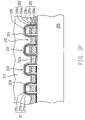
The semiconductor manufacturers have produce one kind of non-volatile memory with a structure shown schematically in FIG. 1. The non-volatile memory includes a memory cell column having a plurality of first memory cells 102 and a plurality of second memory cells 116. The first memory cells 102 are separated from the second memory cells 116 through insulating spacers 110 respectively. Each first memory cell 102 includes a bottom dielectric layer 104 a, a charge-trapping layer 104 b, a top dielectric layer 104 c (the bottom dielectric layer 104 a, the charge-trapping layer 104 b and the top dielectric layer 104 c together form a composite layer 104), a gate 106 and a cap layer 108 sequentially stacked on the substrate 100. Each second memory cell 116 similarly includes a bottom dielectric layer 112 a, a charge-trapping layer 112 b, a top dielectric layer 112 c (the bottom dielectric layer 112 a, the charge-trapping layer 112 b and the top dielectric layer 112 c together form a composite layer 112) and a gate 114 sequentially stacked on the substrate 100. Because there is no gap between neighboring memory cells, the level of integration of devices for this type of non-volatile memory is increased.
However, the gates 106 of the first memory cells 102 are fabricated from a polycide material that includes a doped polysilicon layer 106 a and a metal silicide layer 106 b. On the other hand, the gates 114 of the second memory cells 116 are fabricated from a doped polysilicon material. Since the doped polysilicon material has a resistance much greater than the polycide material, there is a significant difference in the electrical performance between the first memory cells 102 and the second memory cells 116. Hence, there will be a drop in the electrical performance of the devices and a greater instability in the device process.
SUMMARY OF THE INVENTION
Accordingly, at least one objective of the present invention is to provide a method of fabricating a non-volatile memory that can reduce gate resistance, increase memory cell conductivity and increase device performance and stability.
At least a second objective of the present invention is to provide a method of fabricating a non-volatile memory that can in crease device performance. Furthermore, the fabricating method can simplify the manufacturing process and reduce the production cost.
To achieve these and other advantages and in accordance with the purpose of the invention, as embodied and broadly described herein, the invention provides a method of fabricating a non-volatile memory having the following steps. First, a substrate is provided. Then, a plurality of first memory units is formed on the substrate with every two adjoining first memory units are separated from each other by a gap. Each first memory unit includes a first composite layer, a first gate and a cap layer sequentially formed on the substrate. The first composite layer includes a first dielectric layer, a first charge-trapping layer and a top dielectric layer, for example. Thereafter, a plurality of insulating spacers is formed on the sidewalls of the first memory units. After that, a second composite layer is formed over the substrate. The second composite layer includes a second bottom dielectric layer, a second charge-trapping layer and a second top dielectric layer, for example. Then, a doped polysilicon layer is formed over the substrate to fill the gaps between various first memory units. A portion of the doped polysilicon layer is removed so that the surface of the doped polysilicon layer is at least lower than the top surface of the cap layer and a plurality of trenches is formed between the various first memory units. A metallic layer is formed over the substrate to fill the trenches. Afterwards, a portion of the metallic layer is removed until the second composite layer is exposed. The metallic layer and the doped polysilicon layer together form a plurality of second gates, and the second gates and the second composite layer together form a plurality of second memory units. The second memory units and the first memory units together constitute a memory cell column. Thereafter, a source region and a drain region are formed on the two sides of the memory cell column.
According to the aforementioned method of fabricating the non-volatile memory in the preferred embodiment of the present invention, before the step of forming the metallic layer on the substrate to fill the trenches, further includes forming a barrier layer over the substrate. The barrier layer is a titanium/titanium nitride layer formed by sputtering, for example.
According to the aforementioned method of fabricating the non-volatile memory in the preferred embodiment of the present invention, the metallic layer is fabricated using tungsten or metal silicide compound.
According to the aforementioned method of fabricating the non-volatile memory in the preferred embodiment of the present invention, the method of forming a metallic layer to fill the trenches on the substrate includes performing a sputtering process or chemical vapor deposition process.
According to the aforementioned method of fabricating the non-volatile memory in the preferred embodiment of the present invention, the method of removing a portion of the doped polysilicon layer and removing a portion of the metallic layer includes performing an etching back process.
According to the aforementioned method of fabricating the non-volatile memory in the preferred embodiment of the present invention, the first bottom dielectric layer, the first top dielectric layer, the second bottom dielectric layer, the second top dielectric layer can be fabricated by silicon oxide and the first charge-trapping layer and the second charge-trapping layer can be fabricated by silicon nitride or doped polysilicon, for example.
The present invention also provides an alternative method of fabricating a non-volatile memory including the following steps. First, a substrate is provided. Then, a plurality of first memory units is formed on the substrate with every two adjoining first memory units are separated from each other by a gap. Each first memory unit includes a first composite layer, a first gate and a cap layer sequentially formed on the substrate. The first composite layer includes a first bottom dielectric layer, a first charge-trapping layer and a first top dielectric layer, for example. Thereafter, a plurality of insulating spacers is formed on the sidewalls of the first memory units and then a second composite layer is formed over the substrate. The second composite layer includes a second bottom dielectric layer, a second charge-trapping layer and a second top dielectric layer, for example. After that, a doped polysilicon layer is formed over the substrate to fill the gaps between various first memory units. Then, a portion of the doped polysilicon layer is removed so that the top surface of the doped polysilicon layer is at least below the top surface of the cap layer. Thereafter, a metal silicide layer is formed over the doped polysilicon layer. The metal silicide layer and the doped polysilicon layer together form a plurality of second gates and the second gates and the second composite layer together form a plurality of second memory units. The second memory units and the first memory units together constitute a memory cell column. Then, a source region and a drain region are formed in the substrate on the two sides adjacent to the memory cell column.
According to the aforementioned method of fabricating the non-volatile memory in the preferred embodiment of the present invention, the method of removing a portion of the doped polysilicon layer includes performing an etching back process.
According to the aforementioned method of fabricating the non-volatile memory in the preferred embodiment of the present invention, the method of forming the metal silicide layer over the doped polysilicon layer includes depositing metallic material to form a metallic layer over the substrate. Then, an annealing process is performed so that a portion of the metallic layer and the doped polysilicon layer react to form a metal silicide layer. Thereafter, the metallic layer not participated in the reaction is removed. The metallic layer is fabricated using a refractory metal such as cobalt or titaniun and formed by sputtering, for example.
According to the aforementioned method of fabricating the non-volatile memory in the preferred embodiment of the present invention, the first bottom dielectric layer, the first top dielectric layer, the second bottom dielectric layer and the second top dielectric layer can be fabricated by silicon oxide and the first charge-trapping layer and the second charge-trapping layer can be fabricated by silicon nitride or doped polysilicon, for example.
In the method of fabricating the non-volatile memory according to the present invention, only one photomask is required to define the first memory units and the second memory cells is fabricated without using the conventional photolithographic and etching processes. Therefore, the processing is simplified and the production cost is reduced. Furthermore, using polycide compound to form the gate of the second memory units significantly reduces the gate resistance of the second memory units so that the second memory units can have greater conductivity. The first memory units and the second memory units are electrically comparable. Consequently, the performance and stability of the devices are improved.
It is to be understood that both the foregoing general description and the following detailed description are exemplary, and are intended to provide further explanation of the invention as claimed.
BRIEF DESCRIPTION OF THE DRAWINGS
The accompanying drawings are included to provide a further understanding of the invention, and are incorporated in and constitute a part of this specification. The drawings illustrate embodiments of the invention and, together with the description, serve to explain the principles of the invention.
FIG. 1 is a schematic cross-sectional view showing the structure of a conventional non-volatile memory.
FIGS. 2A through 2G are schematic cross-sectional views showing the steps for fabricating a non-volatile memory according to one preferred embodiment of the present invention.
FIGS. 2H through 2I are schematic cross-sectional views showing the steps for fabricating a non-volatile memory according to another preferred embodiment of the present invention.
DESCRIPTION OF THE PREFERRED EMBODIMENTS
Reference will now be made in detail to the present preferred embodiments of the invention, examples of which are illustrated in the accompanying drawings. Wherever possible, the same reference numbers are used in the drawings and the description to refer to the same or like parts.
FIGS. 2A through 2G ate schematic cross-sectional views showing the steps for fabricating a non-volatile memory according to one preferred embodiment of the present invention. As shown in FIG. 2A, a substrate 200 is provided. Then, a plurality of memory units 207 is formed on the substrate 200 with every two adjoining first memory units 207 are separated from each other by a gap 208. Each memory unit 207 includes a composite layer 201, a gate 203 and a cap layer 205, for example. The method of forming the memory units 207 includes forming a composite dielectric material layer, a gate material layer and an insulating material layer sequentially over the substrate 100 and patterning the aforementioned material layers by performing photolithographic and etching processes.
The composite layer 201 includes a bottom dielectric layer 201 a, a charge-trapping layer 201 b and a top dielectric layer 201 c, for example. The bottom dielectric layer 201 a is a silicon oxide layer formed, for example, by performing a thermal oxidation process. The charge-trapping layer 201 b is a silicon nitride layer formed, for example, by performing a chemical vapor deposition process. The top dielectric layer 201 c is a silicon oxide layer formed, for example, by performing a chemical vapor deposition process. Obviously, the bottom dielectric layer 201 a and the top dielectric layer 201 c can be fabricated from other types of similar materials. Similarly, the material constituting the charge-trapping layer 201 b is not limited to silicon nitride. Other types of material that can trap electric charges, for example, tantalum oxide, titanium-strontium acid, hafnium oxide or doped polysilicon can be used as well.
The gates 203 can be fabricated by polycide material, for example. The method of forming the polycide layer includes forming a doped polysilicon layer 203 a over the substrate 200 and then forming a metal silicide layer 203 b over the doped polysilicon layer 203 a. The metal silicide layer 203 b is formed, for example, by performing a chemical vapor deposition process or a self-aligned silicide process. The cap layer 205 is a silicon oxide layer formed, for example, by performing a chemical vapor deposition process.
As shown in FIG. 2B, a plurality of insulating spacers 209 is formed on the sidewalls of the memory units 207. The insulating spacers 208 are fabricated by silicon nitride or silicon oxide, for example. The insulating spacers 208 are formed, for example, by depositing insulating material over the substrate 200 to form an insulating material layer and then performing an anisotropic etching process so that only a portion of the insulation material layer remains on the sidewalls of the memory units 207.
As shown in FIG. 2C, a composite layer 211 is formed over the substrate 200. The composite layer includes a bottom dielectric layer 211 a, a charge-trapping layer 211 b and a top dielectric layer 211 c, for example. The bottom dielectric layer 211 a is a silicon oxide layer formed, for example, by performing a thermal oxidation process. The charge-trapping layer 211 b is a silicon nitride layer formed, for example, by performing a chemical vapor deposition process. The top dielectric layer 211 c is a silicon oxide layer formed, for example, by performing a chemical vapor deposition process. Obviously, the bottom dielectric layer 211 a and the top dielectric layer 211 c can be fabricated from other types of similar materials. Similarly, the material constituting the charge-trapping layer 211 b is not limited to silicon nitride. Other types of material that can trap charges, for example, tantalum oxide, titanium-strontium acid, hafnium oxide or doped polysilicon can be used as well.
As shown in FIG. 2D, a doped polysilicon layer 213 is formed over the substrate 200 to fill the gaps 208 between various memory units 207. The doped polysilicon layer 213 is formed, for example, by depositing an undoped polysilicon layer in a chemical vapor deposition and performing an ion implanting process thereafter.
As shown in FIG. 2E, a portion of the doped polysilicon layer 213 is removed to form a plurality of trenches 215 between the memory units 207. The top surface of the doped polysilicon layer 213 a is at least lower than the top surface of the cap layer 205. The method of removing a portion of the doped polysilicon layer 213 includes performing an etching back process, for example. The depth of the trenches 215 can be controlled through adjusting the time of the etching back process.
As shown in FIG. 2F, a metallic layer 217 is formed over the substrate 200 to fill the trenches 215. The metallic layer 217 is a tungsten layer formed by sputtering, for example. However, the metallic layer 217 can be fabricated by metal silicide such as tungsten metal silicide in a chemical vapor deposition process. Furthermore, a material may be deposited over the substrate 200 to form an additional barrier layer 216 before forming the metallic layer 217 over the substrate 200 to fill the trenches 215. The barrier layer 216 can be a titanium/titanium nitride layer formed by sputtering, for example.
As shown in FIG. 2G, a portion of the metallic layer 217 is removed until the composite layer 211 is exposed. The method of removing a portion of the metallic layer 217 includes performing an etching back process, a chemical-mechanical polishing or some other suitable process. If the embodiment of the present invention includes forming a barrier layer 216, a portion of the barrier layer 216 is removed while removing a portion of the metallic layer 217 to expose the composite layer 211. The metallic layer 217 a together with the doped polysilicon layer 213 a form a gate 219, and the gate 219 together with the composite layer 211 form a memory unit 221. The memory units 211 and the memory units 207 together constitute a memory cell column. Thereafter, any residual gate material 219 in the area designated for forming the source region and the drain region on each side of the memory cell column is removed. The method of removing residual gate material 219 includes performing an etching process, for example. After that, a source region 231 a and a drain region 231 b are formed in the substrate on the two sides adjacent to the memory cell column. The step of forming the source region 231 a and the drain region 231 b includes implanting p-type ions or n-type ions, according to the actual desired device state, into the substrate in an ion implant process, for example.
In the aforementioned embodiment, the gate 219 includes the metallic layer 217 a and the doped polysilicon layer 213 a. Since the metallic layer 217 a can be a tungsten layer or a metal silicide layer, the electrical resistance of the gate 219 is significantly reduced. Furthermore, by forming a barrier layer over the doped polysilicon layer 213 a, the ohmic contact with the doped polysilicon layer 213 a is improved. In addition, the adhesive strength between the metallic layer 217 a and the doped polysilicon layer 213 a is reinforced to bring down the gate resistance so that the gate 219 can have a higher electrical conductivity. Thus, the electrical property of the gates 219 and the gates 203 is more compatible with each other and the performance of the devices is improved.
FIGS. 2H through 2I are schematic cross-sectional views showing the steps for fabricating a non-volatile memory according to another preferred embodiment of the present invention. FIG. 2H is a continuation from FIG. 2D. A portion of the doped polysilicon layer 213 is removed so that the top surface of the doped polysilicon layer 213 b is at least lower than the top surface of the cap layer 205. The step of removing a portion of the doped polysilicon layer 213 includes performing an etching back process.
As shown in FIG. 2I, a metal silicide layer 241 is formed over the doped polysilicon layer 213 b. The method of forming the metal silicide layer 241 includes performing a self-aligned metal silicide process including the following steps. First, a metallic layer (not shown) made from a refractory metal such as cobalt or titanium is formed over the substrate 200, for example, by sputtering. Thereafter, a thermal process is performed so that a portion of the metallic layer reacts with the doped polysilicon layer 213 b to form the metal silicide layer 241. After that, the metallic material in the metallic layer not participated in the reaction is removed.
The metal silicide layers 241 together with the doped polysilicon layers 213 b form a plurality of gates 243, and the gates 243 together with the composite layer 211 form a plurality of memory units 245. The memory units 245 and the memory units 207 together constitute a memory cell column. Thereafter, any residual gate material 243 in the area designated for forming the source region and the drain region on each side of the memory cell column is removed. The method of removing residual gate material 243 includes performing an etching process, for example. After that, a source region 247 a and a drain region 247 b are formed in the substrate 200 on the two sides adjacent to the memory cell column. The step of forming the source region 247 a and the drain region 247 b includes implanting p-type ions or n-type ions, according to the actual desired device state, into the substrate in an ion implant process, for example.
In the aforementioned embodiment, the gate 243 includes the metal silicide layer 241 and the doped polysilicon layer 213 b. Hence, the resistance of the gate 243 is reduced. In addition, the metal silicide layer 241 is formed in a self-aligned metal silicide process. Therefore, no additional photomask is required. Consequently, the process for forming the non-volatile memory is simplified and the production cost is reduced.
In summary, the gate of the memory unit in the method of fabricating the non-volatile memory according to the present invention includes the doped polysilicon layer 213 a and the metallic layer 217 a as shown in FIG. 2G. Alternatively, the gate of the memory unit includes the doped polysilicon layer 213 b and the metal silicide layer 241 as shown in FIG. 2I. Since only a single photomask is required to define the memory units 207 and there is no need to perform photolithographic and etching processes to fabricate the gate of another memory unit, the processing is simplified and the production cost is reduced.
Moreover, the gate of the memory unit is a composite layer including a doped polysilicon layer together with a metallic layer or a metal silicide layer. Hence, the gate resistance is reduced and gate conductivity is increased so that the electrical properties of the memory units 245 and the memory units 207 are compatible with each other. Ultimately, the device performance and stability is improved.
It will be apparent to those skilled in the art that various modifications and variations can be made to the structure of the present invention without departing from the scope or spirit of the invention. In view of the foregoing, it is intended that the present invention cover modifications and variations of this invention provided they fall within the scope of the following claims and their equivalents.

Claims (8)

1. A method of fabricating a non-volatile memory, comprising the steps of:
providing a substrate;
forming a plurality of first memory units on the substrate with every adjoining first memory units are separated from each other by a gap, wherein each first memory unit comprises a first composite layer, a first gate and a cap layer sequentially stacked on the substrate and the first composite layer comprises a first bottom dielectric layer, a first charge-trapping layer and a first top dielectric layer;
forming a plurality of insulating spacers on the sidewalls of the first memory units;
forming a second composite layer over the substrate, wherein the second composite layer comprises a second bottom dielectric layer, a second charge-trapping layer and a second top dielectric layer;
forming a doped polysilicon layer over the substrate, wherein the doped polysilicon layer fills the gaps between various first memory units;
removing a portion of the doped polysilicon layer so that the top surface of the doped polysilicon layer is at least lower than the top surface of the cap layer;
forming a metal silicide layer over the doped polysilicon layer, wherein the metal silicide layer together with the doped polysilicon layer form a plurality of second gates, the second gates together with the second composite layer form a plurality of second memory units, and the second memory units together with the first memory units constitute a memory cell column; and
forming a source region and a drain region in the substrate on the two sides of the memory cell column.
2. The method of claim 1, wherein the step of forming the metal silicide layer over the doped polysilicon layer comprises:
forming a metallic layer over the substrate;
performing an annealing process such that a portion of the metallic layer reacts with the doped polysilicon layer to form the metal silicide layer; and
removing any residual metallic layer not participated in the reaction.
3. The method of claim 2, wherein the material constituting the metallic layer comprises refractory metal.
4. The method of claim 3, wherein the material constituting the metallic layer comprises cobalt or titanium.
5. The method of claim 3, wherein the step of forming the metallic layer over the substrate comprises performing a sputtering process.
6. The method of claim 3, wherein the step of removing a portion of the doped polysilicon layer comprises performing a etching back process.
7. The method of claim 1, wherein the material constituting the first bottom dielectric layer, the first top dielectric layer, the second bottom dielectric layer and the second top dielectric layer comprises silicon oxide.
8. The method of claim 1, wherein the material constituting the first charge-trapping layer and the second charge-trapping layer comprises silicon nitride or doped polysilicon.
US11/558,453 2005-03-02 2006-11-10 Method of fabricating non-volatile memory Active US7285463B2 (en)

Priority Applications (1)

Application Number Priority Date Filing Date Title
US11/558,453 US7285463B2 (en) 2005-03-02 2006-11-10 Method of fabricating non-volatile memory

Applications Claiming Priority (4)

Application Number Priority Date Filing Date Title
TW94106211 2005-03-02
TW094106211A TWI256109B (en) 2005-03-02 2005-03-02 Method of fabricating non-volatile memory
US11/161,648 US7166512B2 (en) 2005-03-02 2005-08-11 Method of fabricating non-volatile memory
US11/558,453 US7285463B2 (en) 2005-03-02 2006-11-10 Method of fabricating non-volatile memory

Related Parent Applications (1)

Application Number Title Priority Date Filing Date
US11/161,648 Division US7166512B2 (en) 2005-03-02 2005-08-11 Method of fabricating non-volatile memory

Related Child Applications (1)

Application Number Title Priority Date Filing Date
US13/915,156 Division US20130274833A1 (en) 2003-05-28 2013-06-11 Micro-organism reducing device

Publications (2)

Publication Number Publication Date
US20070066008A1 US20070066008A1 (en) 2007-03-22
US7285463B2 true US7285463B2 (en) 2007-10-23

Family

ID=36944610

Family Applications (2)

Application Number Title Priority Date Filing Date
US11/161,648 Active US7166512B2 (en) 2005-03-02 2005-08-11 Method of fabricating non-volatile memory
US11/558,453 Active US7285463B2 (en) 2005-03-02 2006-11-10 Method of fabricating non-volatile memory

Family Applications Before (1)

Application Number Title Priority Date Filing Date
US11/161,648 Active US7166512B2 (en) 2005-03-02 2005-08-11 Method of fabricating non-volatile memory

Country Status (2)

Country Link
US (2) US7166512B2 (en)
TW (1) TWI256109B (en)

Families Citing this family (2)

* Cited by examiner, † Cited by third party
Publication number Priority date Publication date Assignee Title
CN100449736C (en) * 2006-07-10 2009-01-07 中芯国际集成电路制造(上海)有限公司 Making method for memory separation grid
US7915660B2 (en) * 2009-05-19 2011-03-29 Powerchip Semiconductor Corp. Junction-free NAND flash memory and fabricating method thereof

Citations (1)

* Cited by examiner, † Cited by third party
Publication number Priority date Publication date Assignee Title
US7238974B2 (en) * 2004-10-29 2007-07-03 Infineon Technologies Ag Semiconductor device and method of producing a semiconductor device

Family Cites Families (1)

* Cited by examiner, † Cited by third party
Publication number Priority date Publication date Assignee Title
KR100200713B1 (en) * 1996-06-25 1999-06-15 윤종용 Method of manufacturing semiconductor device

Patent Citations (1)

* Cited by examiner, † Cited by third party
Publication number Priority date Publication date Assignee Title
US7238974B2 (en) * 2004-10-29 2007-07-03 Infineon Technologies Ag Semiconductor device and method of producing a semiconductor device

Also Published As

Publication number Publication date
US7166512B2 (en) 2007-01-23
TWI256109B (en) 2006-06-01
US20070066008A1 (en) 2007-03-22
US20060199333A1 (en) 2006-09-07
TW200633139A (en) 2006-09-16

Similar Documents

Publication Publication Date Title
US7071061B1 (en) Method for fabricating non-volatile memory
US7445993B2 (en) Method of fabricating non-volatile memory
JP4989630B2 (en) Array source line in NAND flash memory
US7442998B2 (en) Non-volatile memory device
US7186607B2 (en) Charge-trapping memory device and method for production
US20070155087A1 (en) Method of manufacturing split gate flash memory
US20060128102A1 (en) Manufacturing method of an non-volatile memory cell
US6737322B2 (en) Method for manufacturing semiconductor device
US7952133B2 (en) Flash memory and method for manufacturing the same
US7094648B2 (en) Method for fabricating an NROM memory cell array
US7485919B2 (en) Non-volatile memory
US7285463B2 (en) Method of fabricating non-volatile memory
US8536011B2 (en) Junction leakage suppression in memory devices
US20070077754A1 (en) Contact spacer formation using atomic layer deposition
US20060063329A1 (en) Method of fabricating a non-volatile memory
US7271062B2 (en) Non-volatile memory cell and fabricating method thereof and method of fabricating non-volatile memory
JP2010135561A (en) Nonvolatile semiconductor storage device
US20090206390A1 (en) Semiconductor nonvolatile memory device with inter-gate insulating film formed on the side surface of a memory cell and method for manufacturing the same
US20080020529A1 (en) Non-volatile memory and fabrication thereof
EP1017088A1 (en) Selective salicization process for semiconductor devices
US7285450B2 (en) Method of fabricating non-volatile memory
US7772639B2 (en) Charge-trap nonvolatile memory devices
EP1665373A2 (en) Manufacture of a non-volatile memory device with a single access gate and differently doped source and drain
US20050064662A1 (en) [method of fabricating flash memory]
JP2010278062A (en) Semiconductor memory device

Legal Events

Date Code Title Description
STCF Information on status: patent grant

Free format text: PATENTED CASE

AS Assignment

Owner name: POWERCHIP TECHNOLOGY CORPORATION, TAIWAN

Free format text: CHANGE OF NAME;ASSIGNOR:POWERCHIP SEMICONDUCTOR CORP.;REEL/FRAME:024812/0700

Effective date: 20100810

FPAY Fee payment

Year of fee payment: 4

FPAY Fee payment

Year of fee payment: 8

MAFP Maintenance fee payment

Free format text: PAYMENT OF MAINTENANCE FEE, 12TH YEAR, LARGE ENTITY (ORIGINAL EVENT CODE: M1553); ENTITY STATUS OF PATENT OWNER: LARGE ENTITY

Year of fee payment: 12

AS Assignment

Owner name: POWERCHIP SEMICONDUCTOR MANUFACTURING CORPORATION,

Free format text: ASSIGNMENT OF ASSIGNORS INTEREST;ASSIGNOR:POWERCHIP TECHNOLOGY CORPORATION;REEL/FRAME:049757/0575

Effective date: 20190628