US7307119B2 - Thin film material using pentaerythritol acrylate for encapsulation of organic or polymeric light emitting device, and encapsulation method for LED using the same - Google Patents
Thin film material using pentaerythritol acrylate for encapsulation of organic or polymeric light emitting device, and encapsulation method for LED using the same Download PDFInfo
- Publication number
- US7307119B2 US7307119B2 US10/628,253 US62825303A US7307119B2 US 7307119 B2 US7307119 B2 US 7307119B2 US 62825303 A US62825303 A US 62825303A US 7307119 B2 US7307119 B2 US 7307119B2
- Authority
- US
- United States
- Prior art keywords
- encapsulation
- emitting device
- organic
- light emitting
- thin film
- Prior art date
- Legal status (The legal status is an assumption and is not a legal conclusion. Google has not performed a legal analysis and makes no representation as to the accuracy of the status listed.)
- Active, expires
Links
- 239000010409 thin film Substances 0.000 title claims abstract description 18
- 239000000463 material Substances 0.000 title claims abstract description 17
- ZCZFEIZSYJAXKS-UHFFFAOYSA-N [3-hydroxy-2,2-bis(hydroxymethyl)propyl] prop-2-enoate Chemical compound OCC(CO)(CO)COC(=O)C=C ZCZFEIZSYJAXKS-UHFFFAOYSA-N 0.000 title claims abstract description 7
- 238000000034 method Methods 0.000 title abstract description 39
- 238000005538 encapsulation Methods 0.000 title abstract description 30
- 239000000178 monomer Substances 0.000 claims abstract description 17
- 229920000642 polymer Polymers 0.000 claims abstract description 16
- 229920002959 polymer blend Polymers 0.000 claims abstract description 5
- 229920006029 tetra-polymer Polymers 0.000 claims abstract description 3
- -1 poly(pentaerythritol acrylate) Polymers 0.000 claims description 28
- 238000006116 polymerization reaction Methods 0.000 claims description 7
- 238000001035 drying Methods 0.000 abstract description 4
- 238000004519 manufacturing process Methods 0.000 abstract description 3
- NIXOWILDQLNWCW-UHFFFAOYSA-M Acrylate Chemical compound [O-]C(=O)C=C NIXOWILDQLNWCW-UHFFFAOYSA-M 0.000 abstract 1
- 230000008569 process Effects 0.000 description 15
- 230000000052 comparative effect Effects 0.000 description 11
- 239000011521 glass Substances 0.000 description 11
- 238000004020 luminiscence type Methods 0.000 description 11
- 239000000203 mixture Substances 0.000 description 10
- 239000000758 substrate Substances 0.000 description 8
- QVGXLLKOCUKJST-UHFFFAOYSA-N atomic oxygen Chemical compound [O] QVGXLLKOCUKJST-UHFFFAOYSA-N 0.000 description 6
- 229910052760 oxygen Inorganic materials 0.000 description 6
- 239000001301 oxygen Substances 0.000 description 6
- 230000002745 absorbent Effects 0.000 description 5
- 239000002250 absorbent Substances 0.000 description 5
- CBOIHMRHGLHBPB-UHFFFAOYSA-N hydroxymethyl Chemical group O[CH2] CBOIHMRHGLHBPB-UHFFFAOYSA-N 0.000 description 5
- 229910052751 metal Inorganic materials 0.000 description 5
- 239000002184 metal Substances 0.000 description 5
- 230000003287 optical effect Effects 0.000 description 5
- 230000035515 penetration Effects 0.000 description 5
- 239000011248 coating agent Substances 0.000 description 4
- 238000000576 coating method Methods 0.000 description 4
- 239000003505 polymerization initiator Substances 0.000 description 4
- 238000001771 vacuum deposition Methods 0.000 description 4
- 0 [1*]C([2*])([3*])COCC([4*])([5*])[6*] Chemical compound [1*]C([2*])([3*])COCC([4*])([5*])[6*] 0.000 description 3
- 230000000694 effects Effects 0.000 description 3
- 239000000243 solution Substances 0.000 description 3
- 238000004528 spin coating Methods 0.000 description 3
- TVIVIEFSHFOWTE-UHFFFAOYSA-K tri(quinolin-8-yloxy)alumane Chemical compound [Al+3].C1=CN=C2C([O-])=CC=CC2=C1.C1=CN=C2C([O-])=CC=CC2=C1.C1=CN=C2C([O-])=CC=CC2=C1 TVIVIEFSHFOWTE-UHFFFAOYSA-K 0.000 description 3
- OYPRJOBELJOOCE-UHFFFAOYSA-N Calcium Chemical compound [Ca] OYPRJOBELJOOCE-UHFFFAOYSA-N 0.000 description 2
- FYYHWMGAXLPEAU-UHFFFAOYSA-N Magnesium Chemical compound [Mg] FYYHWMGAXLPEAU-UHFFFAOYSA-N 0.000 description 2
- VYPSYNLAJGMNEJ-UHFFFAOYSA-N Silicium dioxide Chemical compound O=[Si]=O VYPSYNLAJGMNEJ-UHFFFAOYSA-N 0.000 description 2
- 229910021536 Zeolite Inorganic materials 0.000 description 2
- 229910052783 alkali metal Inorganic materials 0.000 description 2
- 150000001340 alkali metals Chemical class 0.000 description 2
- 230000000903 blocking effect Effects 0.000 description 2
- 229910052791 calcium Inorganic materials 0.000 description 2
- 239000011575 calcium Substances 0.000 description 2
- 238000005229 chemical vapour deposition Methods 0.000 description 2
- 230000006866 deterioration Effects 0.000 description 2
- HNPSIPDUKPIQMN-UHFFFAOYSA-N dioxosilane;oxo(oxoalumanyloxy)alumane Chemical compound O=[Si]=O.O=[Al]O[Al]=O HNPSIPDUKPIQMN-UHFFFAOYSA-N 0.000 description 2
- 238000010438 heat treatment Methods 0.000 description 2
- 230000000977 initiatory effect Effects 0.000 description 2
- 230000001678 irradiating effect Effects 0.000 description 2
- 239000007788 liquid Substances 0.000 description 2
- 229910052749 magnesium Inorganic materials 0.000 description 2
- 239000011777 magnesium Substances 0.000 description 2
- 238000002156 mixing Methods 0.000 description 2
- 238000005240 physical vapour deposition Methods 0.000 description 2
- 239000000741 silica gel Substances 0.000 description 2
- 229910002027 silica gel Inorganic materials 0.000 description 2
- 238000012719 thermal polymerization Methods 0.000 description 2
- 239000010457 zeolite Substances 0.000 description 2
- JIGUQPWFLRLWPJ-UHFFFAOYSA-N C=CC(=O)OCC Chemical compound C=CC(=O)OCC JIGUQPWFLRLWPJ-UHFFFAOYSA-N 0.000 description 1
- AQUSAYWPMBLCJI-UHFFFAOYSA-N CCC(C1N)=C1N Chemical compound CCC(C1N)=C1N AQUSAYWPMBLCJI-UHFFFAOYSA-N 0.000 description 1
- ODINCKMPIJJUCX-UHFFFAOYSA-N Calcium oxide Chemical compound [Ca]=O ODINCKMPIJJUCX-UHFFFAOYSA-N 0.000 description 1
- 239000004593 Epoxy Substances 0.000 description 1
- 239000007983 Tris buffer Substances 0.000 description 1
- 239000002253 acid Substances 0.000 description 1
- NIXOWILDQLNWCW-UHFFFAOYSA-N acrylic acid group Chemical group C(C=C)(=O)O NIXOWILDQLNWCW-UHFFFAOYSA-N 0.000 description 1
- 239000000853 adhesive Substances 0.000 description 1
- 230000001070 adhesive effect Effects 0.000 description 1
- QVQLCTNNEUAWMS-UHFFFAOYSA-N barium oxide Chemical compound [Ba]=O QVQLCTNNEUAWMS-UHFFFAOYSA-N 0.000 description 1
- RWCCWEUUXYIKHB-UHFFFAOYSA-N benzophenone Chemical compound C=1C=CC=CC=1C(=O)C1=CC=CC=C1 RWCCWEUUXYIKHB-UHFFFAOYSA-N 0.000 description 1
- 239000012965 benzophenone Substances 0.000 description 1
- 230000008859 change Effects 0.000 description 1
- 238000005234 chemical deposition Methods 0.000 description 1
- 229920001688 coating polymer Polymers 0.000 description 1
- 229920001577 copolymer Polymers 0.000 description 1
- 238000000151 deposition Methods 0.000 description 1
- KPUWHANPEXNPJT-UHFFFAOYSA-N disiloxane Chemical class [SiH3]O[SiH3] KPUWHANPEXNPJT-UHFFFAOYSA-N 0.000 description 1
- 238000002474 experimental method Methods 0.000 description 1
- 239000010408 film Substances 0.000 description 1
- AMGQUBHHOARCQH-UHFFFAOYSA-N indium;oxotin Chemical compound [In].[Sn]=O AMGQUBHHOARCQH-UHFFFAOYSA-N 0.000 description 1
- 239000003999 initiator Substances 0.000 description 1
- 238000002347 injection Methods 0.000 description 1
- 239000007924 injection Substances 0.000 description 1
- 239000004973 liquid crystal related substance Substances 0.000 description 1
- 125000000040 m-tolyl group Chemical group [H]C1=C([H])C(*)=C([H])C(=C1[H])C([H])([H])[H] 0.000 description 1
- 238000012986 modification Methods 0.000 description 1
- 230000004048 modification Effects 0.000 description 1
- 238000000465 moulding Methods 0.000 description 1
- 238000005289 physical deposition Methods 0.000 description 1
- 239000000376 reactant Substances 0.000 description 1
- 230000004044 response Effects 0.000 description 1
- 229920002545 silicone oil Polymers 0.000 description 1
- 238000003892 spreading Methods 0.000 description 1
- 230000007480 spreading Effects 0.000 description 1
- ODHXBMXNKOYIBV-UHFFFAOYSA-N triphenylamine Chemical compound C1=CC=CC=C1N(C=1C=CC=CC=1)C1=CC=CC=C1 ODHXBMXNKOYIBV-UHFFFAOYSA-N 0.000 description 1
Images


Classifications
-
- C—CHEMISTRY; METALLURGY
- C09—DYES; PAINTS; POLISHES; NATURAL RESINS; ADHESIVES; COMPOSITIONS NOT OTHERWISE PROVIDED FOR; APPLICATIONS OF MATERIALS NOT OTHERWISE PROVIDED FOR
- C09D—COATING COMPOSITIONS, e.g. PAINTS, VARNISHES OR LACQUERS; FILLING PASTES; CHEMICAL PAINT OR INK REMOVERS; INKS; CORRECTING FLUIDS; WOODSTAINS; PASTES OR SOLIDS FOR COLOURING OR PRINTING; USE OF MATERIALS THEREFOR
- C09D4/00—Coating compositions, e.g. paints, varnishes or lacquers, based on organic non-macromolecular compounds having at least one polymerisable carbon-to-carbon unsaturated bond ; Coating compositions, based on monomers of macromolecular compounds of groups C09D183/00 - C09D183/16
-
- H—ELECTRICITY
- H10—SEMICONDUCTOR DEVICES; ELECTRIC SOLID-STATE DEVICES NOT OTHERWISE PROVIDED FOR
- H10K—ORGANIC ELECTRIC SOLID-STATE DEVICES
- H10K2102/00—Constructional details relating to the organic devices covered by this subclass
- H10K2102/301—Details of OLEDs
- H10K2102/311—Flexible OLED
-
- H—ELECTRICITY
- H10—SEMICONDUCTOR DEVICES; ELECTRIC SOLID-STATE DEVICES NOT OTHERWISE PROVIDED FOR
- H10K—ORGANIC ELECTRIC SOLID-STATE DEVICES
- H10K50/00—Organic light-emitting devices
- H10K50/80—Constructional details
- H10K50/84—Passivation; Containers; Encapsulations
- H10K50/844—Encapsulations
-
- H—ELECTRICITY
- H10—SEMICONDUCTOR DEVICES; ELECTRIC SOLID-STATE DEVICES NOT OTHERWISE PROVIDED FOR
- H10K—ORGANIC ELECTRIC SOLID-STATE DEVICES
- H10K50/00—Organic light-emitting devices
- H10K50/80—Constructional details
- H10K50/84—Passivation; Containers; Encapsulations
- H10K50/846—Passivation; Containers; Encapsulations comprising getter material or desiccants
Definitions
- the present invention is directed to a thin film material for encapsulation of organic or polymeric light-emitting device and a method for encapsulation of the organic or polymeric light-emitting device using the same.
- Organic light-emitting devices have advantages, a wide viewing angle, a short response time, a high contrast ratio, a high light-emitting efficiency, but also have disadvantages, a short life-time compared to that of conventional LCD (liquid crystal display), and a difficulty in adjustment of color balance due to the differences of life-time between LED devices of red, green and blue.
- LCD liquid crystal display
- glass or metal lid containing moisture absorbent e.g, calcium oxide (CaO), or barium oxide (BaO), and so on
- moisture absorbent e.g, calcium oxide (CaO), or barium oxide (BaO), and so on
- the above encapsulation method implicates problems, such as, difficulties in lightening and thinning (>2 mm) of the device, and moreover, it is impossible to materialize bendable next generation of LED by the above method using the glass or metal lid.
- the object of the present invention is to provide novel thin film material for encapsulation to block the penetration of moisture and oxygen, which cause deterioration of the organic or polymeric light emitting device, in order to elongate the lifetime of the device.
- the second object of the present invention is to provide a method for encapsulation of organic or polymeric light emitting device using said thin film material, which method is simple and low cost, and can ensure reliability and processibility of organic organic light-emitting devices.
- the organic light-emitting device is generally manufactured by a process comprising that, on a glass or plastic transparent substrate, depositing in succession, under vacuum condition, cathode of ITO(Indium Tin Oxide), hole transporting layer, light emitting layer(organics or polymer), electron transporting layer and electron transporting electrode, thereafter, encapsulating by coating polymer on the outside of the light-emitting device.
- ITO Indium Tin Oxide
- hole transporting layer hole transporting layer
- light emitting layer(organics or polymer) electron transporting layer and electron transporting electrode
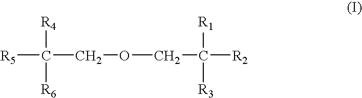
- first object of the present invention can be achieved by polymer having, as repeating unit of backbone, one to four pentaerythritol acrylate monomers represented by formula I or formula II, depicted as below, that is, homo-polymer from one monomer, co-polymer from two monomer, ter-polymer from three monomer, or tetra-polymer from four monomer:
- R1, R 2 , R 3 , R 4 , R 5 and R6 are
- R6 is CH 2 OH; or R1, R2, R3, and R4 are
- R5, and R6 are CH 2 OH; or R1, R2, and R3 are
- R4, R5, and R6 are CH 2 OH; or R1, and R2 are
- R3, R4, R5, and R6 are CH 2 OH;
- R7, R8, R9, and R10 is
- Poly(pentaerythritol acrylate) for encapsulation of organic or polymeric light-emitting device polymerized from the monomers dipicted as formula I or II, has superior adhesiveness to the glass or plastic substrate compared to conventional thin film material for encapsulation, and encapsulated organic or polymeric light-emitting device has superior flexibility.
- One to four monomer depicted as formula I or II, used for polymerization of poly(pentaerythritol acrylate) for encapsulation of organic or polymeric light-emitting device, according to the present invention may be used in the range from 0.1 to 99.9 wt % based on total weight of reactant.
- the first object of the present invention also can be achieved by physically mixed polymer blend of said poly(pentaerythritol acrylate) and other polymers.
- Polymers other than poly(pentaerythritol acrylate) may be used in the polymer blend in the range from 0.1 to 99.0 wt % based on the total weight of the polymer blend.
- the thin film material for encapsulation may be further comprise moisture absorbent, for example, magnesium. calcium, silica gel, zeolite or alkali metal.
- moisture absorbent for example, magnesium. calcium, silica gel, zeolite or alkali metal.
- the other object of the present invention is to providing a method for encapsulating organic or polymeric light-emitting device using said poly(pentaerythritol acrylate).
- the encapsulation method is divided into wet process and dry process.
- the wet process comprises the steps of mixing poly(pentaerythritol acrylate) monomer(s) represented by formula 1 or formula 2, and optical or thermal polymerization initiator in the range of 0.01 to 99 wt % of based on the total weight of a mixture; coating the mixture on the organic or polymeric light-emitting device using said poly(pentaerythritol acrylate) by direct spin coating, bar coating, spreading or immersing the device into the mixture; and initiating polymerization step by irradiating ultraviolet ray to the mixture or heating the mixture.
- the wet process may be accomplished by adding polymer(s) other than poly(pentaerythritol acrylate) in the range of 0.01 to 99 wt % based on the total weight of polymer, or by adding moisture absorbents, such as magnesium, calcium, silica gel, zeolite or other alkali metal.
- moisture absorbents such as magnesium, calcium, silica gel, zeolite or other alkali metal.
- the dry process comprises the steps of mixing poly(pentaerythritol acrylate) monomer(s) represented by formula 1 or formula 2, and optical or thermal polymerization initiator in the range of 0.01 to 99 wt % of based on the total weight of a mixture; coating the mixture on the organic or polymeric light-emitting device using said poly(pentaerythritol acrylate) by PVD (physical vapor deposition) or CVD (chemical vapor deposition) method; and initiating polymerization step by irradiating ultraviolet ray to the the mixture or heating the mixture.
- the wet process may be accomplished by adding polymer(s) other than poly(pentaerythritol acrylate) in the range of 0.01 to 99 wt % based on the total weight of polymer.
- FIG. 1 is a drawing showing a cross-sectional view of light-emitting device encapsulated according to the present invention.
- FIG. 2 is a graph showing test results on the effect of lifetime elongation of light-emitting device encapsulated according to the present invention in comparison with the comparative example.
- transparent glass or plastic materials may be used as substrate( 1 ).
- ITO electrode( 2 ) was coated on the substrate( 1 ), thereafter, hole transporting layer( 3 ) was formed on the ITO electrode( 2 ).
- light-emitting layer( 4 ) and electron transporting layer( 5 ) were coated on the hole transporting layer( 3 ) by vacuum deposition process.
- Representative electron transportating material having light emitting property for light-emitting layer( 4 ) and electron transporting layer( 5 ) is Alq3 (tris(8-quinolinolato)aluminum).
- metal electrode for anode was deposited on the center of the light-emitting layer( 4 ) and electron transporting layer( 5 ).
- the layers ( 3 ) and ( 5 ) can be omitted.
- a light emitting device having a layered structure depicted in the FIG. 1 was prepared by following procedures. First, ITO electrode of 0.2 ⁇ m thickness was formed on a glass substrate, then, hole injection layer of 20 nm thickness composed of MTDATA (4,4′,4′′-tris(N-3(3-methylphenyl)-N-phenylamino)triphenylamine) and hole transporting layer of 40 nm thickness composed of NPB (N,N′-biphenyl-N,N′-bis(1-naphentyl)-(1,1′-biphenyl-4,4′-diamine) were formed in turn. Thereafter, green light emitting layer of 60 nm thickness was formed by vacuum deposition of Alq3. On the said light emitting layer, metal electrode for anode composed of 1.2 nm thick LiF and 70 nm thick Al was formed by vacuum deposition. Above described procedures can be established by conventional known process.
- liquid pentaerythrithol monomer 100 parts by weight of liquid pentaerythrithol monomer and 10 parts by weight of polymerization initiator(HSP188) was coated in 8 ⁇ 9 ⁇ m thickness on the said layered structure by conventional spin coating process under atmospheric condition. Then, at room temperature and under atmospheric pressure, polymerization reaction was initiated by radiating UV light of 500 mJ/cm2 intensity on the said coating of organic solution, so that a encapsulation thin film was formed.
- Said liquid pentaerythrithol monomer commercially available from SKUCB corp., is a multifunctional liquidous monomer containing a mixture of tri- and tetra-acrylates with a high degree of acrylic unsaturation, has viscosity at 25° C.
- Said initiator also commercially available from SKUCB corp. under the trademark HSP188, is an optical polymerization initiator belonging to a benzophenone family, and can initiate the optical polymerization when radiating energy greater than 100 mJ/cm2.
- a light emitting device having same structure with the above-made light emitting device except for not forming encapsulation thin film was prepared following the same procedure as above-mentioned method.
- the effect of the encapsulation according to the present invention on the elongation of the light emitting device was evaluated by measuring the luminescence change of the encapsulated light emitting device according to the present invention and non-encapsulated light emitting device of comparative example 1.
- lifetime is defined as time taken to decrease the luminescence to half of the initial luminescence.
- the initial luminescence of the light emitting device according to the example 1 of the present invention is equal to that of the comparative example 1, and, no decrease of the initial luminescence was occurred.
- the lifetime of the light emitting device according to the example 1 of the present invention is elongated much more than that of the comparative example 1. Namely, the lifetime of the light emitting device according to the example 1 of the present invention is much longer than that of the comparative example 1 by more than 3 times.
- the encapsulation step was performed under the atmospheric condition, however, the encapsulation step may be performed under the inert condition, under which condition, oxygen and moisture will be removed. Better result can be expected when the encapsulation step is performed under the inert condition.
- a light emitting device was prepared following the same procedure as Example 1, except for that PET plastic substrate was used instead of glass substrate, and that NPB layer of 100 nm thickness on the Al electode to improve the stability of the light emitting device. Same light emitting device as Comparative Example 1 was prepared as Comparative Example 2. The lifetime for light emitting devices of Example 2 and Comparative Example 2 were measured following the same procedure and under the same condition except for the temperature was room temperature.
- the encapsulated light emitting device according to the example 2 of the present invention has lifetime of 367 hours, but the non-encpsulated comparative example 2 has lifetime of 108 hours.
- the encapsulation thin film of the invention is valid for the plastic-based light emitting device, as well as glass-based light emitting device.
- the thin film for encapsulation of organic or polymeric light emitting device By using the thin film for encapsulation of organic or polymeric light emitting device according to the present invention, penetration of oxygen and moisture into the light emitting device, so that the lifetime of the light emitting device can be elongated.
- the light emitting device encapsulated by the thin film of the present invention has so superior flexibility that the encapsulated device can be applied in the manufacturing of the flexible display.
- the encapsulation method of the present invention does not need a separate expensive equipment, in practice, such as vacuum pump, and may form protection film in simple manner, thus, the manufacturing process is simple, so that the productivity can be improved.
Abstract
Description

wherein:
or R1, R2, R3, R4, and R5 are
and R6 is CH2OH; or R1, R2, R3, and R4 are
and R5, and R6 are CH2OH; or R1, R2, and R3 are
and R4, R5, and R6 are CH2OH; or R1, and R2 are
and R3, R4, R5, and R6 are CH2OH;

wherein:
and the remainder of the group are CH2OH.
| TABLE 1 | ||||
| Initial | lifetime | |||
| Sample | luminescence(cd/m2) | (hr) | ||
| Example 1 | 170 | 7.4 | ||
| Comparative | 170 | 2.3 | ||
| Example 1 | ||||
Claims (3)
Priority Applications (1)
| Application Number | Priority Date | Filing Date | Title |
|---|---|---|---|
| US11/979,303 US20080114117A1 (en) | 2002-01-08 | 2007-11-01 | Thin film material using pentaerythritol acrylate for encapsulation of organic or polymeric light emitting device, and encapsulation method for LED using the same |
Applications Claiming Priority (4)
| Application Number | Priority Date | Filing Date | Title |
|---|---|---|---|
| KR2002-45479 | 2002-08-01 | ||
| KR20020045479 | 2002-08-01 | ||
| KR10-2003-0047638A KR100503828B1 (en) | 2002-08-01 | 2003-07-12 | Thin Film Material using Pentaerithritol acrylate for Encapsulation of Organic or Polymeric Electronic Light Emitting Device, and Encapsulation Method for LED |
| KR2003-47638 | 2003-07-12 |
Related Child Applications (1)
| Application Number | Title | Priority Date | Filing Date |
|---|---|---|---|
| US11/979,303 Division US20080114117A1 (en) | 2002-01-08 | 2007-11-01 | Thin film material using pentaerythritol acrylate for encapsulation of organic or polymeric light emitting device, and encapsulation method for LED using the same |
Publications (2)
| Publication Number | Publication Date |
|---|---|
| US20040024105A1 US20040024105A1 (en) | 2004-02-05 |
| US7307119B2 true US7307119B2 (en) | 2007-12-11 |
Family
ID=31190427
Family Applications (2)
| Application Number | Title | Priority Date | Filing Date |
|---|---|---|---|
| US10/628,253 Active 2024-12-15 US7307119B2 (en) | 2002-01-08 | 2003-07-29 | Thin film material using pentaerythritol acrylate for encapsulation of organic or polymeric light emitting device, and encapsulation method for LED using the same |
| US11/979,303 Abandoned US20080114117A1 (en) | 2002-01-08 | 2007-11-01 | Thin film material using pentaerythritol acrylate for encapsulation of organic or polymeric light emitting device, and encapsulation method for LED using the same |
Family Applications After (1)
| Application Number | Title | Priority Date | Filing Date |
|---|---|---|---|
| US11/979,303 Abandoned US20080114117A1 (en) | 2002-01-08 | 2007-11-01 | Thin film material using pentaerythritol acrylate for encapsulation of organic or polymeric light emitting device, and encapsulation method for LED using the same |
Country Status (1)
| Country | Link |
|---|---|
| US (2) | US7307119B2 (en) |
Cited By (5)
| Publication number | Priority date | Publication date | Assignee | Title |
|---|---|---|---|---|
| CN102651456A (en) * | 2012-03-27 | 2012-08-29 | 京东方科技集团股份有限公司 | Thin-film packaging component, photoelectronic device and packaging method of photoelectronic device |
| US9070838B2 (en) | 2011-06-10 | 2015-06-30 | Samsung Electronics Co., Ltd. | Optoelectronic device and stacking structure |
| US20170062762A1 (en) | 2015-08-31 | 2017-03-02 | Kateeva, Inc. | Di- and Mono(Meth)Acrylate Based Organic Thin Film Ink Compositions |
| US9909022B2 (en) | 2014-07-25 | 2018-03-06 | Kateeva, Inc. | Organic thin film ink compositions and methods |
| US11844234B2 (en) | 2017-04-21 | 2023-12-12 | Kateeva, Inc. | Compositions and techniques for forming organic thin films |
Families Citing this family (16)
| Publication number | Priority date | Publication date | Assignee | Title |
|---|---|---|---|---|
| US7112351B2 (en) * | 2002-02-26 | 2006-09-26 | Sion Power Corporation | Methods and apparatus for vacuum thin film deposition |
| KR100475849B1 (en) * | 2002-04-17 | 2005-03-10 | 한국전자통신연구원 | Organic electroluminescent devices having encapsulation thin film formed by wet processing and methods for manufacturing the same |
| FR2875995B1 (en) * | 2004-09-24 | 2014-10-24 | Oberthur Card Syst Sa | METHOD FOR MOUNTING AN ELECTRONIC COMPONENT ON A SUPPORT, PREFERABLY MOU, AND ELECTRONIC ENTITY THUS OBTAINED, SUCH AS A PASSPORT |
| FR2924940B1 (en) * | 2007-12-13 | 2012-10-19 | Oreal | COSMETIC COMPOSITION COMPRISING MACADAMIA OIL AND A WAX. |
| US20130226268A1 (en) | 2010-07-26 | 2013-08-29 | Merck Patent Gmbh | Nanocrystals in devices |
| WO2012110178A1 (en) | 2011-02-14 | 2012-08-23 | Merck Patent Gmbh | Device and method for treatment of cells and cell tissue |
| JP6356060B2 (en) | 2011-03-24 | 2018-07-11 | メルク パテント ゲーエムベーハー | Organic ionic functional materials |
| US9496502B2 (en) | 2011-05-12 | 2016-11-15 | Merck Patent Gmbh | Organic ionic compounds, compositions and electronic devices |
| US9290618B2 (en) | 2011-08-05 | 2016-03-22 | Sabic Global Technologies B.V. | Polycarbonate compositions having enhanced optical properties, methods of making and articles comprising the polycarbonate compositions |
| WO2013116697A1 (en) * | 2012-02-03 | 2013-08-08 | Sabic Innovative Plastics Ip B.V. | Light emitting diode device and method for production thereof containing conversion material chemistry |
| EP2819981B1 (en) | 2012-02-29 | 2016-12-21 | SABIC Global Technologies B.V. | Process for producing low sulfur bisphenol a, processes for producing polycarbonate, articles made from polycarbonate |
| WO2014066784A1 (en) | 2012-10-25 | 2014-05-01 | Sabic Innovative Plastics Ip B.V. | Light emitting diode devices, method of manufacture, uses thereof |
| WO2014191943A1 (en) | 2013-05-29 | 2014-12-04 | Sabic Innovative Plastics Ip B.V. | Illuminating devices with color stable thermoplastic light-transmitting articles |
| CN105470401B (en) * | 2015-11-24 | 2017-12-08 | 武汉理工大学 | A kind of preparation method of the perovskite solar cell based on silk rod blade coating |
| EP3455326B1 (en) | 2016-05-11 | 2021-02-24 | Merck Patent GmbH | Compositions for electrochemical cells |
| CN111129362B (en) * | 2019-12-31 | 2021-04-27 | 武汉华星光电半导体显示技术有限公司 | Organic light emitting diode and method for manufacturing the same |
Citations (11)
| Publication number | Priority date | Publication date | Assignee | Title |
|---|---|---|---|---|
| US4371566A (en) * | 1980-09-10 | 1983-02-01 | Panelgraphic Corporation | Abrasion resistant coating composition |
| US4414278A (en) * | 1982-04-22 | 1983-11-08 | E. I. Du Pont De Nemours And Company | Crosslinked triacrylate polymer beads |
| US4478876A (en) * | 1980-12-18 | 1984-10-23 | General Electric Company | Process of coating a substrate with an abrasion resistant ultraviolet curable composition |
| JPS644605A (en) * | 1987-06-27 | 1989-01-09 | Daiso Co Ltd | Thermosetting molding material |
| US5734225A (en) | 1996-07-10 | 1998-03-31 | International Business Machines Corporation | Encapsulation of organic light emitting devices using siloxane or siloxane derivatives |
| KR100215768B1 (en) | 1997-06-14 | 1999-08-16 | 구자홍 | Organic Electroluminescence Device |
| US6268695B1 (en) | 1998-12-16 | 2001-07-31 | Battelle Memorial Institute | Environmental barrier material for organic light emitting device and method of making |
| WO2001088041A1 (en) * | 2000-05-17 | 2001-11-22 | Dynic Corporation | Moisture absorbing formed article |
| WO2002055612A1 (en) * | 2001-01-15 | 2002-07-18 | Dai Nippon Printing Co., Ltd. | Coating composition, coating film thereof, antireflection coating, antireflection film, image display, and intermediate product |
| US6470594B1 (en) * | 2001-09-21 | 2002-10-29 | Eastman Kodak Company | Highly moisture-sensitive electronic device element and method for fabrication utilizing vent holes or gaps |
| US6673385B1 (en) * | 2000-05-31 | 2004-01-06 | Advanced Cardiovascular Systems, Inc. | Methods for polymeric coatings stents |
Family Cites Families (3)
| Publication number | Priority date | Publication date | Assignee | Title |
|---|---|---|---|---|
| JP4260882B2 (en) * | 1995-09-12 | 2009-04-30 | ダウ グローバル テクノロジーズ インコーポレイティド | Ethynyl-substituted aromatic compounds, their synthesis, polymers and uses |
| US6226890B1 (en) * | 2000-04-07 | 2001-05-08 | Eastman Kodak Company | Desiccation of moisture-sensitive electronic devices |
| US6646080B2 (en) * | 2000-09-14 | 2003-11-11 | Dsm N.V. | Coating compositions for plastic substrates |
-
2003
- 2003-07-29 US US10/628,253 patent/US7307119B2/en active Active
-
2007
- 2007-11-01 US US11/979,303 patent/US20080114117A1/en not_active Abandoned
Patent Citations (13)
| Publication number | Priority date | Publication date | Assignee | Title |
|---|---|---|---|---|
| US4371566A (en) * | 1980-09-10 | 1983-02-01 | Panelgraphic Corporation | Abrasion resistant coating composition |
| US4478876A (en) * | 1980-12-18 | 1984-10-23 | General Electric Company | Process of coating a substrate with an abrasion resistant ultraviolet curable composition |
| US4414278A (en) * | 1982-04-22 | 1983-11-08 | E. I. Du Pont De Nemours And Company | Crosslinked triacrylate polymer beads |
| JPS644605A (en) * | 1987-06-27 | 1989-01-09 | Daiso Co Ltd | Thermosetting molding material |
| US5734225A (en) | 1996-07-10 | 1998-03-31 | International Business Machines Corporation | Encapsulation of organic light emitting devices using siloxane or siloxane derivatives |
| KR100215768B1 (en) | 1997-06-14 | 1999-08-16 | 구자홍 | Organic Electroluminescence Device |
| US6268695B1 (en) | 1998-12-16 | 2001-07-31 | Battelle Memorial Institute | Environmental barrier material for organic light emitting device and method of making |
| WO2001088041A1 (en) * | 2000-05-17 | 2001-11-22 | Dynic Corporation | Moisture absorbing formed article |
| US6673436B2 (en) * | 2000-05-17 | 2004-01-06 | Dynic Corporation | Moisture absorbing formed article |
| US6673385B1 (en) * | 2000-05-31 | 2004-01-06 | Advanced Cardiovascular Systems, Inc. | Methods for polymeric coatings stents |
| WO2002055612A1 (en) * | 2001-01-15 | 2002-07-18 | Dai Nippon Printing Co., Ltd. | Coating composition, coating film thereof, antireflection coating, antireflection film, image display, and intermediate product |
| US6949284B2 (en) * | 2001-01-15 | 2005-09-27 | Dai Nippon Printing Co., Ltd. | Coating composition, it's coating layer, antireflection coating, antireflection film, image display and intermediate product |
| US6470594B1 (en) * | 2001-09-21 | 2002-10-29 | Eastman Kodak Company | Highly moisture-sensitive electronic device element and method for fabrication utilizing vent holes or gaps |
Cited By (7)
| Publication number | Priority date | Publication date | Assignee | Title |
|---|---|---|---|---|
| US9070838B2 (en) | 2011-06-10 | 2015-06-30 | Samsung Electronics Co., Ltd. | Optoelectronic device and stacking structure |
| CN102651456A (en) * | 2012-03-27 | 2012-08-29 | 京东方科技集团股份有限公司 | Thin-film packaging component, photoelectronic device and packaging method of photoelectronic device |
| CN102651456B (en) * | 2012-03-27 | 2015-06-24 | 京东方科技集团股份有限公司 | Thin-film packaging component, photoelectronic device and packaging method of photoelectronic device |
| US9909022B2 (en) | 2014-07-25 | 2018-03-06 | Kateeva, Inc. | Organic thin film ink compositions and methods |
| US20170062762A1 (en) | 2015-08-31 | 2017-03-02 | Kateeva, Inc. | Di- and Mono(Meth)Acrylate Based Organic Thin Film Ink Compositions |
| US10190018B2 (en) | 2015-08-31 | 2019-01-29 | Kateeva, Inc. | Di- and mono(meth)acrylate based organic thin film ink compositions |
| US11844234B2 (en) | 2017-04-21 | 2023-12-12 | Kateeva, Inc. | Compositions and techniques for forming organic thin films |
Also Published As
| Publication number | Publication date |
|---|---|
| US20080114117A1 (en) | 2008-05-15 |
| US20040024105A1 (en) | 2004-02-05 |
Similar Documents
| Publication | Publication Date | Title |
|---|---|---|
| US20080114117A1 (en) | Thin film material using pentaerythritol acrylate for encapsulation of organic or polymeric light emitting device, and encapsulation method for LED using the same | |
| JP7203903B2 (en) | Sealant for organic electroluminescence display elements | |
| US7442428B2 (en) | Gas barrier substrate | |
| CN101766055A (en) | Organic electroluminescent device and method for manufacturing the same | |
| CN1265261A (en) | Emissive display using organic light emitting diodes | |
| JP2014203707A (en) | Method of manufacturing organic el display and organic el display | |
| JP3674819B2 (en) | Color filter and organic multicolor light emitting display element | |
| CN109689700B (en) | Composition comprising a metal oxide and a metal oxide | |
| JP7253542B2 (en) | Sealant for organic electroluminescence display elements | |
| TWI582099B (en) | A compound, a desiccant, a sealing structure, and an organic EL element | |
| JP2004537833A (en) | Electrode composition | |
| WO2005091682A1 (en) | Organic el element and process for producing the same | |
| US20040147701A1 (en) | Molecular chemical compounds with structures allowing electron displacement and capable of emitting photoluminescent radiation, and photoluminescence quenching device employing the same | |
| KR100503828B1 (en) | Thin Film Material using Pentaerithritol acrylate for Encapsulation of Organic or Polymeric Electronic Light Emitting Device, and Encapsulation Method for LED | |
| JP2004303562A (en) | Substrate for organic electroluminescent element | |
| KR20030089749A (en) | Organic electroluminescent devices having encapsulation thin film comprising polyamide and methods for manufacturing the same | |
| JP2014067599A (en) | Organic el display, and method of manufacturing the same | |
| WO2021100710A1 (en) | Composition, cured body, sealing material for organic electroluminescent display element, and organic electroluminescent display device | |
| CN102593372A (en) | Flexible top-emitting organic electroluminescent device having ultra-smooth anode | |
| WO2023238270A1 (en) | Light-emitting device | |
| KR100494846B1 (en) | Encapsulated organic light emitting device and method for fabrication thereof | |
| CN100446292C (en) | Organic electrically execiting light-emitting device | |
| KR100554161B1 (en) | Encapsulation thin film materials obtained from tetraoxaspiro or dioxane monomer and encapsulation methods using the same | |
| TW202219232A (en) | Composition for electronic device sealing, method for forming electronic device sealing film, and electronic device sealing film | |
| JP2020138477A (en) | Laminate, method for producing laminate, and organic electroluminescence display device |
Legal Events
| Date | Code | Title | Description |
|---|---|---|---|
| AS | Assignment |
Owner name: ELECTRONICS AND TELECOMMUNICATIONS RESEARCH INSTIT Free format text: ASSIGNMENT OF ASSIGNORS INTEREST;ASSIGNORS:KIM, GI HEON;OH, JI YOUNG;YANG, YONG SUK;AND OTHERS;REEL/FRAME:014339/0573 Effective date: 20030716 |
|
| STCF | Information on status: patent grant |
Free format text: PATENTED CASE |
|
| FEPP | Fee payment procedure |
Free format text: PAYOR NUMBER ASSIGNED (ORIGINAL EVENT CODE: ASPN); ENTITY STATUS OF PATENT OWNER: SMALL ENTITY Free format text: PAYER NUMBER DE-ASSIGNED (ORIGINAL EVENT CODE: RMPN); ENTITY STATUS OF PATENT OWNER: SMALL ENTITY |
|
| FEPP | Fee payment procedure |
Free format text: PAYER NUMBER DE-ASSIGNED (ORIGINAL EVENT CODE: RMPN); ENTITY STATUS OF PATENT OWNER: SMALL ENTITY Free format text: PAYOR NUMBER ASSIGNED (ORIGINAL EVENT CODE: ASPN); ENTITY STATUS OF PATENT OWNER: SMALL ENTITY |
|
| FPAY | Fee payment |
Year of fee payment: 4 |
|
| FPAY | Fee payment |
Year of fee payment: 8 |
|
| MAFP | Maintenance fee payment |
Free format text: PAYMENT OF MAINTENANCE FEE, 12TH YR, SMALL ENTITY (ORIGINAL EVENT CODE: M2553); ENTITY STATUS OF PATENT OWNER: SMALL ENTITY Year of fee payment: 12 |