US7307335B2 - Semiconductor device having MOS varactor and methods for fabricating the same - Google Patents
Semiconductor device having MOS varactor and methods for fabricating the same Download PDFInfo
- Publication number
- US7307335B2 US7307335B2 US11/048,715 US4871505A US7307335B2 US 7307335 B2 US7307335 B2 US 7307335B2 US 4871505 A US4871505 A US 4871505A US 7307335 B2 US7307335 B2 US 7307335B2
- Authority
- US
- United States
- Prior art keywords
- metal
- gate electrode
- semiconductor
- layer
- metal gate
- Prior art date
- Legal status (The legal status is an assumption and is not a legal conclusion. Google has not performed a legal analysis and makes no representation as to the accuracy of the status listed.)
- Active, expires
Links
- 239000004065 semiconductor Substances 0.000 title claims abstract description 130
- 238000000034 method Methods 0.000 title abstract description 24
- 229910052751 metal Inorganic materials 0.000 claims abstract description 127
- 239000002184 metal Substances 0.000 claims abstract description 127
- 239000000758 substrate Substances 0.000 claims abstract description 30
- 239000003990 capacitor Substances 0.000 claims abstract description 21
- 239000010936 titanium Substances 0.000 claims description 7
- NRTOMJZYCJJWKI-UHFFFAOYSA-N Titanium nitride Chemical compound [Ti]#N NRTOMJZYCJJWKI-UHFFFAOYSA-N 0.000 claims description 5
- 239000000463 material Substances 0.000 claims description 4
- RTAQQCXQSZGOHL-UHFFFAOYSA-N Titanium Chemical compound [Ti] RTAQQCXQSZGOHL-UHFFFAOYSA-N 0.000 claims description 3
- MZLGASXMSKOWSE-UHFFFAOYSA-N tantalum nitride Chemical compound [Ta]#N MZLGASXMSKOWSE-UHFFFAOYSA-N 0.000 claims description 3
- 229910052719 titanium Inorganic materials 0.000 claims description 3
- WFKWXMTUELFFGS-UHFFFAOYSA-N tungsten Chemical compound [W] WFKWXMTUELFFGS-UHFFFAOYSA-N 0.000 claims description 3
- 229910052721 tungsten Inorganic materials 0.000 claims description 3
- 239000010937 tungsten Substances 0.000 claims description 3
- 238000004519 manufacturing process Methods 0.000 abstract description 6
- 239000010410 layer Substances 0.000 description 168
- VYPSYNLAJGMNEJ-UHFFFAOYSA-N Silicium dioxide Chemical compound O=[Si]=O VYPSYNLAJGMNEJ-UHFFFAOYSA-N 0.000 description 15
- 239000012535 impurity Substances 0.000 description 10
- 125000006850 spacer group Chemical group 0.000 description 10
- 238000000059 patterning Methods 0.000 description 9
- 229910052581 Si3N4 Inorganic materials 0.000 description 7
- 239000011229 interlayer Substances 0.000 description 7
- 239000000377 silicon dioxide Substances 0.000 description 7
- HQVNEWCFYHHQES-UHFFFAOYSA-N silicon nitride Chemical compound N12[Si]34N5[Si]62N3[Si]51N64 HQVNEWCFYHHQES-UHFFFAOYSA-N 0.000 description 7
- 238000005530 etching Methods 0.000 description 6
- XUIMIQQOPSSXEZ-UHFFFAOYSA-N Silicon Chemical compound [Si] XUIMIQQOPSSXEZ-UHFFFAOYSA-N 0.000 description 5
- 238000000206 photolithography Methods 0.000 description 5
- 229910052710 silicon Inorganic materials 0.000 description 5
- 239000010703 silicon Substances 0.000 description 5
- 238000005468 ion implantation Methods 0.000 description 4
- 235000012239 silicon dioxide Nutrition 0.000 description 4
- PXHVJJICTQNCMI-UHFFFAOYSA-N Nickel Chemical compound [Ni] PXHVJJICTQNCMI-UHFFFAOYSA-N 0.000 description 3
- 239000003989 dielectric material Substances 0.000 description 3
- 150000002500 ions Chemical class 0.000 description 3
- 230000015572 biosynthetic process Effects 0.000 description 2
- 238000000151 deposition Methods 0.000 description 2
- 230000003647 oxidation Effects 0.000 description 2
- 238000007254 oxidation reaction Methods 0.000 description 2
- 229910021420 polycrystalline silicon Inorganic materials 0.000 description 2
- 229920005591 polysilicon Polymers 0.000 description 2
- 238000009825 accumulation Methods 0.000 description 1
- 239000010941 cobalt Substances 0.000 description 1
- 229910017052 cobalt Inorganic materials 0.000 description 1
- GUTLYIVDDKVIGB-UHFFFAOYSA-N cobalt atom Chemical compound [Co] GUTLYIVDDKVIGB-UHFFFAOYSA-N 0.000 description 1
- 238000007796 conventional method Methods 0.000 description 1
- 230000007423 decrease Effects 0.000 description 1
- 238000010438 heat treatment Methods 0.000 description 1
- 239000011810 insulating material Substances 0.000 description 1
- 238000002955 isolation Methods 0.000 description 1
- 238000002844 melting Methods 0.000 description 1
- 230000008018 melting Effects 0.000 description 1
- 229910044991 metal oxide Inorganic materials 0.000 description 1
- 150000004706 metal oxides Chemical class 0.000 description 1
- 229910052759 nickel Inorganic materials 0.000 description 1
- 150000004767 nitrides Chemical class 0.000 description 1
- 229910021332 silicide Inorganic materials 0.000 description 1
- FVBUAEGBCNSCDD-UHFFFAOYSA-N silicide(4-) Chemical compound [Si-4] FVBUAEGBCNSCDD-UHFFFAOYSA-N 0.000 description 1
- 229910052814 silicon oxide Inorganic materials 0.000 description 1
- 239000000126 substance Substances 0.000 description 1
Images


Classifications
-
- H—ELECTRICITY
- H01—ELECTRIC ELEMENTS
- H01L—SEMICONDUCTOR DEVICES NOT COVERED BY CLASS H10
- H01L27/00—Devices consisting of a plurality of semiconductor or other solid-state components formed in or on a common substrate
- H01L27/02—Devices consisting of a plurality of semiconductor or other solid-state components formed in or on a common substrate including semiconductor components specially adapted for rectifying, oscillating, amplifying or switching and having at least one potential-jump barrier or surface barrier; including integrated passive circuit elements with at least one potential-jump barrier or surface barrier
- H01L27/04—Devices consisting of a plurality of semiconductor or other solid-state components formed in or on a common substrate including semiconductor components specially adapted for rectifying, oscillating, amplifying or switching and having at least one potential-jump barrier or surface barrier; including integrated passive circuit elements with at least one potential-jump barrier or surface barrier the substrate being a semiconductor body
- H01L27/08—Devices consisting of a plurality of semiconductor or other solid-state components formed in or on a common substrate including semiconductor components specially adapted for rectifying, oscillating, amplifying or switching and having at least one potential-jump barrier or surface barrier; including integrated passive circuit elements with at least one potential-jump barrier or surface barrier the substrate being a semiconductor body including only semiconductor components of a single kind
- H01L27/0805—Capacitors only
- H01L27/0808—Varactor diodes
-
- H—ELECTRICITY
- H01—ELECTRIC ELEMENTS
- H01R—ELECTRICALLY-CONDUCTIVE CONNECTIONS; STRUCTURAL ASSOCIATIONS OF A PLURALITY OF MUTUALLY-INSULATED ELECTRICAL CONNECTING ELEMENTS; COUPLING DEVICES; CURRENT COLLECTORS
- H01R13/00—Details of coupling devices of the kinds covered by groups H01R12/70 or H01R24/00 - H01R33/00
- H01R13/44—Means for preventing access to live contacts
- H01R13/447—Shutter or cover plate
- H01R13/453—Shutter or cover plate opened by engagement of counterpart
- H01R13/4534—Laterally sliding shutter
-
- H—ELECTRICITY
- H01—ELECTRIC ELEMENTS
- H01L—SEMICONDUCTOR DEVICES NOT COVERED BY CLASS H10
- H01L27/00—Devices consisting of a plurality of semiconductor or other solid-state components formed in or on a common substrate
- H01L27/02—Devices consisting of a plurality of semiconductor or other solid-state components formed in or on a common substrate including semiconductor components specially adapted for rectifying, oscillating, amplifying or switching and having at least one potential-jump barrier or surface barrier; including integrated passive circuit elements with at least one potential-jump barrier or surface barrier
- H01L27/04—Devices consisting of a plurality of semiconductor or other solid-state components formed in or on a common substrate including semiconductor components specially adapted for rectifying, oscillating, amplifying or switching and having at least one potential-jump barrier or surface barrier; including integrated passive circuit elements with at least one potential-jump barrier or surface barrier the substrate being a semiconductor body
- H01L27/08—Devices consisting of a plurality of semiconductor or other solid-state components formed in or on a common substrate including semiconductor components specially adapted for rectifying, oscillating, amplifying or switching and having at least one potential-jump barrier or surface barrier; including integrated passive circuit elements with at least one potential-jump barrier or surface barrier the substrate being a semiconductor body including only semiconductor components of a single kind
- H01L27/0805—Capacitors only
- H01L27/0811—MIS diodes
-
- H—ELECTRICITY
- H01—ELECTRIC ELEMENTS
- H01L—SEMICONDUCTOR DEVICES NOT COVERED BY CLASS H10
- H01L29/00—Semiconductor devices adapted for rectifying, amplifying, oscillating or switching, or capacitors or resistors with at least one potential-jump barrier or surface barrier, e.g. PN junction depletion layer or carrier concentration layer; Details of semiconductor bodies or of electrodes thereof ; Multistep manufacturing processes therefor
- H01L29/66—Types of semiconductor device ; Multistep manufacturing processes therefor
- H01L29/86—Types of semiconductor device ; Multistep manufacturing processes therefor controllable only by variation of the electric current supplied, or only the electric potential applied, to one or more of the electrodes carrying the current to be rectified, amplified, oscillated or switched
- H01L29/92—Capacitors with potential-jump barrier or surface barrier
- H01L29/93—Variable capacitance diodes, e.g. varactors
-
- H—ELECTRICITY
- H01—ELECTRIC ELEMENTS
- H01L—SEMICONDUCTOR DEVICES NOT COVERED BY CLASS H10
- H01L29/00—Semiconductor devices adapted for rectifying, amplifying, oscillating or switching, or capacitors or resistors with at least one potential-jump barrier or surface barrier, e.g. PN junction depletion layer or carrier concentration layer; Details of semiconductor bodies or of electrodes thereof ; Multistep manufacturing processes therefor
- H01L29/66—Types of semiconductor device ; Multistep manufacturing processes therefor
- H01L29/86—Types of semiconductor device ; Multistep manufacturing processes therefor controllable only by variation of the electric current supplied, or only the electric potential applied, to one or more of the electrodes carrying the current to be rectified, amplified, oscillated or switched
- H01L29/92—Capacitors with potential-jump barrier or surface barrier
- H01L29/94—Metal-insulator-semiconductors, e.g. MOS
-
- H—ELECTRICITY
- H01—ELECTRIC ELEMENTS
- H01R—ELECTRICALLY-CONDUCTIVE CONNECTIONS; STRUCTURAL ASSOCIATIONS OF A PLURALITY OF MUTUALLY-INSULATED ELECTRICAL CONNECTING ELEMENTS; COUPLING DEVICES; CURRENT COLLECTORS
- H01R13/00—Details of coupling devices of the kinds covered by groups H01R12/70 or H01R24/00 - H01R33/00
- H01R13/62—Means for facilitating engagement or disengagement of coupling parts or for holding them in engagement
- H01R13/629—Additional means for facilitating engagement or disengagement of coupling parts, e.g. aligning or guiding means, levers, gas pressure electrical locking indicators, manufacturing tolerances
Definitions
- the present invention generally relates to semiconductor devices and methods for fabricating the same. More particularly, the present invention generally relates to semiconductor devices having a metal-oxide semiconductor (MOS) varactor and methods for fabricating the same.
- MOS metal-oxide semiconductor
- a varactor is a voltage-variable capacitor used in analog integrated circuit such as a voltage controlled oscillator (VCO) which is one of the most important circuit blocks for radio frequency (RF) front-end.
- VCO voltage controlled oscillator
- the varactor requires a wide tuning range and a high Q value.
- the varactor integrated in a semiconductor device is generally a junction varactor or a MOS varactor.
- the tuning range in a junction varactor is usually narrower than that of a MOS varactor and does not improve preferably as a CMOS device scales down. Hence, as semiconductor devices become highly integrated, the MOS varactor is more likely becoming a choice in a high frequency integrated circuit.
- U.S. Pat. No. 5,038,184 discloses a conventional method of fabricating a MOS varactor.
- the MOS varactor includes an active semiconductor layer and a gate electrode.
- a capacitor dielectric layer is interposed between the active semiconductor layer and the gate electrode. Therefore, when voltage is applied to the gate electrode, electrical charge accumulates on or depletes from the active semiconductor layer, and accordingly varies the capacitance of the varactor.
- the varactor reaches a maximum capacitance “Cmax”. As electrical charge is fully depleted from the active semiconductor layer, the varactor reaches a minimum capacitance “Cmin”. The ratio of “Cmax” to “Cmin” determines the tuning range.
- the conventional varactor generally employs poly silicon as a gate electrode. Therefore, as electrical charge accumulates in the active semiconductor layer, poly depletion occurs in the gate electrode. The poly depletion in the gate electrode lowers the value of “Cmax”, which decreases the tuning range of the varactor. To increase the tuning range of the varactor, the poly depletion must be suppressed in the gate electrode.
- semiconductor integrated circuits require various resistors.
- a high frequency integrated circuit requires a reliable metal resistor.
- the metal resistor is fabricated by forming and patterning a metal film. A photomask is required to pattern the metal film. The use of an additional photomask increases the manufacturing cost of the semiconductor device.
- the invention is directed to a semiconductor device.
- the semiconductor device includes a semiconductor substrate, a MOS varactor having a metal gate electrode provided on the semiconductor substrate, an active semiconductor plate interposed between the metal gate electrode and the semiconductor substrate, and a capacitor dielectric layer interposed between the metal gate electrode and the active semiconductor plate, a metal resistor disposed on the same plane as the metal gate electrode and being of a same material as the metal gate electrode, and a lower insulating layer insulating the MOS varactor from the semiconductor substrate.
- One embodiment of a method for manufacturing a semiconductor device includes forming a lightly doped semiconductor layer on the lower insulating layer, sequentially forming a dielectric layer and a metal layer on the lightly doped semiconductor layer, forming a metal gate electrode, a capacitor dielectric layer, and an active semiconductor plate having extended portions by patterning the metal layer, the dielectric layer, and the lightly doped semiconductor layer within a first region of the lower insulating layer, forming a metal resistor on the same plane as the metal gate electrode by patterning the metal layer within a second region of the lower insulating layer at the same time the metal layer, the dielectric layer, and the lightly doped semiconductor layer within the first region of the lower insulating layer are patterned, and forming highly doped regions within the active semiconductor plate by implanting impurity ions into the active semiconductor plate, using the metal gate electrode as an ion implantation mask.
- Another embodiment of a method for manufacturing a semiconductor device includes forming a lower insulating layer on a semiconductor substrate, forming a lightly doped semiconductor layer on the lower insulating layer, forming an active semiconductor plate by patterning the lightly doped semiconductor layer within a first region of the lower insulating layer, sequentially forming a dielectric layer and a metal layer on the semiconductor substrate having the active semiconductor plate, forming a metal gate electrode on the active semiconductor plate by sequentially patterning the dielectric layer and the metal layer within the first region of the lower insulating layer, forming a semiconductor resistor by patterning the lightly doped semiconductor layer within a second region of the lower insulating layer at the same time the lightly doped semiconductor layer within the first region of the lower insulating layer are pattern, forming a metal resistor on the semiconductor resistor by sequentially patterning the metal layer and the dielectric layer within the second region of the lower insulating layer at the same time sequentially patterning the metal layer and the dielectric layer within the first region of the lower insulating layer,
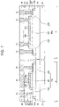
- FIG. 1 is a layout view of a semiconductor device having a MOS varactor according to an embodiment of the present invention.
- FIGS. 2 through 7 are cross-sectional views taken along line I-I of FIG. 1 to illustrate a method of fabricating a semiconductor device according to the embodiment of the present invention.
- A indicates a first region on a semiconductor substrate 21
- B indicates a second region on semiconductor substrate 21 .
- a MOS varactor is formed in first region “A”.
- the MOS varactor includes a metal gate electrode 29 a provided on semiconductor substrate 21 , an active semiconductor plate 25 a interposed between metal gate electrode 29 a and semiconductor substrate 21 , and a capacitor dielectric layer 27 a interposed between metal gate electrode 29 a and active semiconductor plate 25 a . Further, a lower insulating layer 23 is interposed between active semiconductor plate 25 a and semiconductor substrate 21 to insulate the MOS varactor from semiconductor substrate 21 .
- Metal gate electrode 29 a is a metal layer of titanium (Ti), tantalum nitride (TaN), titanium nitride (TiN), or tungsten (W). Further, metal gate electrode 29 a is in contact with capacitor dielectric layer 27 a.
- Capacitor dielectric layer 27 a is formed of silicon dioxide (SiO 2 ), but may also be formed of any other high-k dielectric material such as silicon nitride (SiN). The higher the dielectric constant of capacitor dielectric layer 27 a , the wider the tuning range of the MOS varactor. Metal gate electrode 29 a and capacitor dielectric layer 27 a are aligned with each other.
- Active semiconductor plate 25 a includes extended portions.
- extended portions means the portions of active semiconductor plate 25 a extending away from the alignment of the metal gate electrode 27 a and capacitor dielectric layer 27 a .
- the length of the active semiconductor plate is longer than the capacitor dielectric layer 27 a and metal gate electrode 29 a . Therefore, high concentrations of impurities are implanted in the extended portions to form a ground electrode.
- active semiconductor plate 25 a includes lightly doped region 24 l and highly doped regions 24 h . Highly doped regions 24 h is preferably used as the ground electrodes for active semiconductor plate 25 a.
- Lower insulating layer 23 is provided on semiconductor substrate 21 . That is, lower insulating layer 23 is formed by depositing an insulating layer on semiconductor substrate 21 . An oxidation process or a shallow trench isolation (STI) process may be used in the formation of the insulating layer. Lower insulating layer 23 formed by the oxidation or the STI process is generally referred to as a field oxide layer. Preferably, lower insulating layer 23 is a field oxide layer formed by the STI process.
- STI shallow trench isolation
- a metal resistor 29 b is provided on second region “B” of semiconductor substrate 21 .
- Metal resistor 29 b is provided on the same plane as metal gate electrode 29 a . Further, metal resistor 29 b is made of the same material as metal gate electrode 29 a.
- a semiconductor resistor 25 b is interposed between metal resistor 29 b and semiconductor substrate 21 .
- Semiconductor resistor 25 b is provided on the same plane as active semiconductor plate 25 a .
- Semiconductor resistor 25 b also includes extended portions, which extend beyond metal resistor 29 b .
- Semiconductor resistor 25 b also includes lightly doped region 26 l and highly doped regions 26 h . Highly doped regions 26 h are preferably used as electrodes for semiconductor resistor 25 b.
- a patterned dielectric layer 27 b is interposed between metal resistor 29 b and semiconductor resistor 25 b .
- Patterned dielectric layer 27 b is made of the same material as capacitor dielectric layer 27 a.
- First spacers 31 a cover sidewalls of metal gate electrode 29 a and capacitor dielectric layer 27 a .
- First spacers 31 a also cover sidewalls of metal resistor 29 b and patterned dielectric layer 27 b .
- second spacers 31 b cover sidewalls of active semiconductor plate 25 a and semiconductor resistor 25 b.
- Self-aligned silicide layers (or salicide layers) 33 are provided on the extension portions of active semiconductor plate 25 a and semiconductor resistor 25 b .
- Metal interconnection lines 41 are disposed above metal gate electrode 29 a and extension portions of active semiconductor plate 25 a .
- Metal interconnection lines 41 are disposed across both sides of metal resistor 29 b and semiconductor resistor 25 b .
- metal interconnection lines 41 are electrically connected to salicide layers 33 , metal gate electrode 29 a , and metal resistor 29 b through a plurality of via holes 37 .
- the plurality of via holes 37 are preferably used to electrically connect metal gate electrode 29 a with metal interconnection line 41 .
- Spaces between metal interconnection line 41 and the plurality of via holes 37 are filled with an interlayer insulating layer 35 and an upper insulating layer 39 .
- a metal gate electrode is used to form the varactor, which prevents poly depletion. Further, the metal resistor is formed at the same time the metal gate electrode is formed, which integrates a reliable metal resistor in a semiconductor device without the need of an additional photomask.
- a lower insulating layer 23 is formed on a semiconductor substrate 21 .
- Lower insulating layer 23 is formed by depositing an insulating material on semiconductor substrate 21 .
- lower insulating layer 23 is formed by a STI process. That is, semiconductor substrate 21 is patterned to form a trench. An insulating layer fills the trench, and the insulating layer is planarized to form lower insulating layer 23 .
- lightly doped layer 25 is formed on lower insulating layer 23 .
- Lightly doped layer 25 is preferably lightly doped silicon layer.
- a silicon layer is formed on lower insulating layer 23 , and then low concentration of impurities is implanted into the silicon layer by an ion implantation process to form a lightly doped silicon layer.
- the silicon layer is a poly silicon layer.
- Dielectric layer 27 is formed of silicon dioxide (SiO 2 ), or may be formed of any other high-k dielectric material such as silicon nitride (SiN). Dielectric layer 27 is preferably formed of a stacked layer of silicon dioxide and silicon nitride.
- Metal layer 29 is formed of metal nitride such as a tantalum nitride (TaN) or a titanium nitride (TiN), or a metal having a high melting point such as tungsten (W).
- Metal layer 29 is preferably formed of a stacked layer of Ti and TiN.
- metal layer 29 , dielectric layer 27 , and lightly doped layer 25 are patterned within first region “A” to form a metal gate electrode 29 a , a capacitor dielectric layer 27 a , and an active semiconductor plate 25 a having extended portions.
- metal layer 29 , dielectric layer 27 , and lightly doped layer 25 are patterned as follows.
- Metal layer 29 and dielectric layer 27 within first region “A” are sequentially patterned using a photolithography process and an etching process to form metal gate electrode 29 a and capacitor dielectric layer 27 a .
- metal layer 29 within second region “B” is patterned to form a metal resistor 29 b and a patterned dielectric layer 27 b .
- lightly doped layer 25 is patterned by a photolithography process and an etching process to form an active semiconductor plate 25 a and a semiconductor resistor 25 b.
- metal layer 29 , dielectric layer 27 , and lightly doped semiconductor layer 25 are continuously patterned using sequential photolithography and etching processes to form active semiconductor plate 25 a .
- metal layer 29 and dielectric layer 27 in second region “B” are simultaneously formed and patterned. That is, patterned metal layer 29 and patterned dielectric layer 27 may be patterned using sequential photolithography and etching processes to form metal gate electrode 29 a and capacitor dielectric layer 27 a . Further, metal layer 29 , dielectric layer 27 , and lightly doped semiconductor layer 25 within second region “B” are patterned in the same manner. On the other hand, if semiconductor resistor 25 b is not required, the process of continuously patterning metal layer 29 , dielectric layer 27 , and lightly doped semiconductor layer 25 within second region “B” may be omitted.
- Active semiconductor plate 25 a and semiconductor resistor 25 b may be formed prior to the formation of dielectric layer 27 . That is, after forming lightly doped semiconductor layer 25 , lightly doped semiconductor layer 25 is patterned by a photolithography process and an etching process to form active semiconductor plate 25 a and semiconductor resistor 25 b . Then, dielectric layer 27 and metal layer 29 are sequentially formed. Then, metal layer 29 and dielectric layer 27 are sequentially patterned to form metal gate electrode 29 a and capacitor dielectric layer 27 a . At the same time, metal resistor 29 b and patterned dielectric layer 27 b may be formed.
- a spacer insulating layer (not shown) is formed on metal gate electrode 29 a , active semiconductor plate 25 a , metal resistor 29 b , and patterned dielectric layer 27 b .
- the spacer insulating layer may be of silicon nitride, or a stacked layer of silicon oxide and silicon nitride.
- the spacer insulating layer is etched to form first spacers 31 a covering sidewalls of metal gate electrode 29 a and capacitor dielectric layer 27 a .
- second spacers 31 b are formed to cover sidewalls of active semiconductor plate 25 a and semiconductor resistor 25 b.
- Impurity ions are implanted into active semiconductor plate 25 a and semiconductor resistor 25 b , using spacers 31 a , metal gate electrode 29 a , and metal resistor 29 b as an ion implantation mask to form highly doped regions 24 h , 26 h .
- highly doped regions 24 h , 26 h are formed, lightly doped regions 24 l , 26 l are formed under metal gate electrode 29 a and metal resistor 29 b , respectively.
- Highly doped regions 24 h formed within active semiconductor plate 25 a are preferably used as a ground electrode.
- Highly doped regions 24 h , 26 h are preferably doped with the same type of impurities as those of lightly doped regions 24 l , 26 l . That is, in the case where lightly doped regions 24 l , 26 l are doped with N-type impurities, highly doped regions 24 h , 26 h are also doped with N-type impurities. Oppositely, in the case where lightly doped regions 24 l , 26 l are doped with P-type impurities, highly doped regions 24 h , 26 h are also doped with P-type impurities.
- a metal layer of nickel (Ni), cobalt (Co), or titanium (Ti) is formed on highly doped regions 24 h , 26 h . Then, the metal layer is subjected to heat treatment to form salicide layers 33 . Salicide layers 33 are self-aligned on highly doped regions 24 h , 26 h . After forming salicide layers 33 , any remaining residual metal layer is removed.
- Interlayer insulating layer 35 is formed on salicide layers 33 .
- Interlayer insulating layer 35 is preferably silicon dioxide (SiO 2 ) or some other low-k dielectric material.
- Interlayer insulating layer 35 is patterned to form a plurality of via holes 37 to expose salicide layers 33 , metal gate electrode 29 a , and metal resistor 29 b . Then, a metal layer fills the plurality of via holes 37 . Then, the metal layer is planarized to expose the top surface of interlayer insulating layer.
- metal layer is planarized by a blanket etching or a chemical mechanical planarization (CMP) process.
- An upper metal layer is formed on the plurality via holes 37 , and patterned to form metal interconnection lines 41 over via holes 37 .
- Metal interconnection line 41 electrically connected to metal gate electrode 29 a is used as a signal line.
- an upper insulating layer 39 is formed on semiconductor substrate having metal interconnection lines 41 and then planarized to fill spaces between metal interconnection lines 41 .
- metal interconnection lines 41 are preferably formed by a damascene process. That is, upper insulating layer 39 is formed on semiconductor substrate having the plurality of via holes 37 . Then, upper insulating layer 39 is patterned to form grooves above the plurality of via holes 37 . Thereafter, grooves are filled with an upper conductive layer, and then the upper conductive layer is planarized to form metal interconnection lines 41 in the grooves.
- the plurality of via holes 37 and metal interconnection lines 41 are also preferably formed by a dual-damascene process. That is, upper insulating layer 39 is formed on interlayer insulating layer 35 . Then, interlayer insulating layer 35 and upper insulating layer 39 are patterned to form via holes through which salicide layers 33 , gate electrode 29 a , and metal resistor 29 b are exposed to form the grooves crossing above the via holes. Thereafter, the via holes and the grooves are filled with an upper metal layer, and then the upper metal layer is planarized to form via holes 37 and metal interconnection lines 41 .
Abstract
Description
Claims (8)
Priority Applications (1)
| Application Number | Priority Date | Filing Date | Title |
|---|---|---|---|
| US11/941,192 US7611956B2 (en) | 2004-02-12 | 2007-11-16 | Semiconductor device having MOS varactor and methods for fabricating the same |
Applications Claiming Priority (2)
| Application Number | Priority Date | Filing Date | Title |
|---|---|---|---|
| KR1020040009380A KR100593444B1 (en) | 2004-02-12 | 2004-02-12 | Semiconductor device having MOS varistor and method for manufacturing same |
| KR2004-9380 | 2004-02-12 |
Related Child Applications (1)
| Application Number | Title | Priority Date | Filing Date |
|---|---|---|---|
| US11/941,192 Division US7611956B2 (en) | 2004-02-12 | 2007-11-16 | Semiconductor device having MOS varactor and methods for fabricating the same |
Publications (2)
| Publication Number | Publication Date |
|---|---|
| US20050179113A1 US20050179113A1 (en) | 2005-08-18 |
| US7307335B2 true US7307335B2 (en) | 2007-12-11 |
Family
ID=34836726
Family Applications (2)
| Application Number | Title | Priority Date | Filing Date |
|---|---|---|---|
| US11/048,715 Active 2025-06-14 US7307335B2 (en) | 2004-02-12 | 2005-02-03 | Semiconductor device having MOS varactor and methods for fabricating the same |
| US11/941,192 Expired - Fee Related US7611956B2 (en) | 2004-02-12 | 2007-11-16 | Semiconductor device having MOS varactor and methods for fabricating the same |
Family Applications After (1)
| Application Number | Title | Priority Date | Filing Date |
|---|---|---|---|
| US11/941,192 Expired - Fee Related US7611956B2 (en) | 2004-02-12 | 2007-11-16 | Semiconductor device having MOS varactor and methods for fabricating the same |
Country Status (3)
| Country | Link |
|---|---|
| US (2) | US7307335B2 (en) |
| KR (1) | KR100593444B1 (en) |
| CN (1) | CN100449758C (en) |
Cited By (4)
| Publication number | Priority date | Publication date | Assignee | Title |
|---|---|---|---|---|
| US20100117133A1 (en) * | 2007-04-05 | 2010-05-13 | Chartered Semiconductor Manufacturing, Ltd. | Mos varactors with large tuning range |
| US20110143459A1 (en) * | 2004-03-19 | 2011-06-16 | Fujitsu Semiconductor Limited | Semiconductor substrate and method of fabricating semiconductor device |
| US20130168817A1 (en) * | 2011-11-07 | 2013-07-04 | Renesas Electronics Corporation | Semiconductor device and method for manufacturing the same |
| US20180198000A1 (en) * | 2015-10-30 | 2018-07-12 | Globalfoundries Inc. | Semiconductor structure including a varactor and method for the formation thereof |
Families Citing this family (20)
| Publication number | Priority date | Publication date | Assignee | Title |
|---|---|---|---|---|
| KR100615099B1 (en) * | 2005-02-28 | 2006-08-22 | 삼성전자주식회사 | Semiconductor device including resistor and method of fabricating the same |
| US7560798B2 (en) * | 2006-02-27 | 2009-07-14 | International Business Machines Corporation | High performance tapered varactor |
| US8450832B2 (en) * | 2007-04-05 | 2013-05-28 | Globalfoundries Singapore Pte. Ltd. | Large tuning range junction varactor |
| TW200849759A (en) * | 2007-06-08 | 2008-12-16 | Univ Chang Gung | Cascade EMP protection circuit |
| US7741187B2 (en) * | 2007-09-20 | 2010-06-22 | Chartered Semiconductor Manufacturing, Ltd. | Lateral junction varactor with large tuning range |
| TWI445241B (en) * | 2008-03-21 | 2014-07-11 | Univ Chang Gung | Electromagnetic pulse protection circuit with filtering function |
| US8605404B2 (en) | 2008-06-06 | 2013-12-10 | Chang Gung University | Cascade electromagnetic pulse protection circuit for high frequency application |
| US9111779B2 (en) * | 2008-08-07 | 2015-08-18 | Texas Instruments Incorporated | IC resistor formed with integral heatsinking structure |
| US20100052072A1 (en) * | 2008-08-28 | 2010-03-04 | Taiwan Semiconductor Manufacturing Company, Ltd. | Dual gate structure on a same chip for high-k metal gate technology |
| CN102064175B (en) * | 2009-11-11 | 2013-05-22 | 中国科学院微电子研究所 | Semiconductor structure and manufacturing method thereof |
| CN102244000B (en) * | 2011-06-23 | 2016-07-06 | 上海华虹宏力半导体制造有限公司 | Semiconductor device, varactor and forming method thereof |
| CN102420258A (en) * | 2011-07-12 | 2012-04-18 | 上海华力微电子有限公司 | Structure of metal-insulator-metal MOS (Metal Oxide Semiconductor) capacitor and manufacturing method of structure |
| CN103035480A (en) * | 2011-10-10 | 2013-04-10 | 中芯国际集成电路制造(上海)有限公司 | Semiconductor device and manufacturing method thereof |
| TWI550885B (en) * | 2012-10-31 | 2016-09-21 | 天鈺科技股份有限公司 | Semiconductor capacitor and semiconductor capacitor device using same |
| US9012966B2 (en) | 2012-11-21 | 2015-04-21 | Qualcomm Incorporated | Capacitor using middle of line (MOL) conductive layers |
| US9502586B1 (en) * | 2015-09-14 | 2016-11-22 | Qualcomm Incorporated | Backside coupled symmetric varactor structure |
| US10263065B2 (en) | 2015-11-04 | 2019-04-16 | Globalfoundries Inc. | Metal resistor forming method using ion implantation |
| US10333007B2 (en) * | 2017-06-19 | 2019-06-25 | Qualcomm Incorporated | Self-aligned contact (SAC) on gate for improving metal oxide semiconductor (MOS) varactor quality factor |
| US11121129B2 (en) * | 2018-07-31 | 2021-09-14 | Taiwan Semiconductor Manufacturing Company, Ltd. | Semiconductor device |
| CN110112223B (en) * | 2019-05-20 | 2022-05-20 | 西安理工大学 | TSV (through silicon via) -based accumulation type MOS (metal oxide semiconductor) varactor and preparation method thereof |
Citations (14)
| Publication number | Priority date | Publication date | Assignee | Title |
|---|---|---|---|---|
| US3590340A (en) * | 1967-02-27 | 1971-06-29 | Hitachi Ltd | Breakdown preventing circuit and an integrated device thereof for a semiconductor device having an insulate gate electrode |
| US4285001A (en) * | 1978-12-26 | 1981-08-18 | Board Of Trustees Of Leland Stanford Jr. University | Monolithic distributed resistor-capacitor device and circuit utilizing polycrystalline semiconductor material |
| US5038184A (en) * | 1989-11-30 | 1991-08-06 | Xerox Corporation | Thin film varactors |
| US5210438A (en) * | 1989-05-18 | 1993-05-11 | Fujitsu Limited | Semiconductor resistance element and process for fabricating same |
| US5489547A (en) * | 1994-05-23 | 1996-02-06 | Texas Instruments Incorporated | Method of fabricating semiconductor device having polysilicon resistor with low temperature coefficient |
| US6172378B1 (en) * | 1999-05-03 | 2001-01-09 | Silicon Wave, Inc. | Integrated circuit varactor having a wide capacitance range |
| US6191018B1 (en) * | 1999-01-04 | 2001-02-20 | Taiwan Semiconductor Manufacturing Company | Method for selective resistivity adjustment of polycide lines for enhanced design flexibility and improved space utilization in sub-micron integrated circuits |
| US6246084B1 (en) * | 1997-12-05 | 2001-06-12 | Hyundai Electronics Industries Co., Ltd. | Method for fabricating semiconductor device comprising capacitor and resistor |
| KR20010064440A (en) | 1999-12-29 | 2001-07-09 | 박종섭 | Method for forming NMOS type varactor |
| US6518642B2 (en) * | 2001-06-06 | 2003-02-11 | Samsung Electronics Co., Ltd. | Integrated circuit having a passive device integrally formed therein |
| US20030047782A1 (en) * | 2001-09-07 | 2003-03-13 | Hisashi Hasegawa | Complementary MOS semiconductor device |
| US20030127691A1 (en) * | 2002-01-07 | 2003-07-10 | Honeywell International Inc. | Varactor with improved tuning range |
| US6603172B1 (en) * | 1996-06-17 | 2003-08-05 | Matsushita Electric Industrial Co., Ltd. | Semiconductor device and method of manufacturing the same |
| US20030183880A1 (en) * | 2002-03-27 | 2003-10-02 | Yoshiro Goto | Semiconductor device covering transistor and resistance with capacitor material |
Family Cites Families (5)
| Publication number | Priority date | Publication date | Assignee | Title |
|---|---|---|---|---|
| US5965912A (en) * | 1997-09-03 | 1999-10-12 | Motorola, Inc. | Variable capacitor and method for fabricating the same |
| KR100317538B1 (en) | 1999-12-06 | 2001-12-24 | 김윤규, 정주영, 심옥진, 정몽헌 | Low temperature heat treatment and calcium compound used pollution deposit treating method |
| KR20010086499A (en) | 2000-03-02 | 2001-09-13 | 윤종용 | Method of forming semiconductor device with soi substrate |
| US6423632B1 (en) * | 2000-07-21 | 2002-07-23 | Motorola, Inc. | Semiconductor device and a process for forming the same |
| US7034653B2 (en) | 2004-01-30 | 2006-04-25 | Agere Systems Inc. | Semiconductor resistor |
-
2004
- 2004-02-12 KR KR1020040009380A patent/KR100593444B1/en active IP Right Grant
-
2005
- 2005-02-03 US US11/048,715 patent/US7307335B2/en active Active
- 2005-02-08 CN CNB2005100783515A patent/CN100449758C/en not_active Expired - Fee Related
-
2007
- 2007-11-16 US US11/941,192 patent/US7611956B2/en not_active Expired - Fee Related
Patent Citations (14)
| Publication number | Priority date | Publication date | Assignee | Title |
|---|---|---|---|---|
| US3590340A (en) * | 1967-02-27 | 1971-06-29 | Hitachi Ltd | Breakdown preventing circuit and an integrated device thereof for a semiconductor device having an insulate gate electrode |
| US4285001A (en) * | 1978-12-26 | 1981-08-18 | Board Of Trustees Of Leland Stanford Jr. University | Monolithic distributed resistor-capacitor device and circuit utilizing polycrystalline semiconductor material |
| US5210438A (en) * | 1989-05-18 | 1993-05-11 | Fujitsu Limited | Semiconductor resistance element and process for fabricating same |
| US5038184A (en) * | 1989-11-30 | 1991-08-06 | Xerox Corporation | Thin film varactors |
| US5489547A (en) * | 1994-05-23 | 1996-02-06 | Texas Instruments Incorporated | Method of fabricating semiconductor device having polysilicon resistor with low temperature coefficient |
| US6603172B1 (en) * | 1996-06-17 | 2003-08-05 | Matsushita Electric Industrial Co., Ltd. | Semiconductor device and method of manufacturing the same |
| US6246084B1 (en) * | 1997-12-05 | 2001-06-12 | Hyundai Electronics Industries Co., Ltd. | Method for fabricating semiconductor device comprising capacitor and resistor |
| US6191018B1 (en) * | 1999-01-04 | 2001-02-20 | Taiwan Semiconductor Manufacturing Company | Method for selective resistivity adjustment of polycide lines for enhanced design flexibility and improved space utilization in sub-micron integrated circuits |
| US6172378B1 (en) * | 1999-05-03 | 2001-01-09 | Silicon Wave, Inc. | Integrated circuit varactor having a wide capacitance range |
| KR20010064440A (en) | 1999-12-29 | 2001-07-09 | 박종섭 | Method for forming NMOS type varactor |
| US6518642B2 (en) * | 2001-06-06 | 2003-02-11 | Samsung Electronics Co., Ltd. | Integrated circuit having a passive device integrally formed therein |
| US20030047782A1 (en) * | 2001-09-07 | 2003-03-13 | Hisashi Hasegawa | Complementary MOS semiconductor device |
| US20030127691A1 (en) * | 2002-01-07 | 2003-07-10 | Honeywell International Inc. | Varactor with improved tuning range |
| US20030183880A1 (en) * | 2002-03-27 | 2003-10-02 | Yoshiro Goto | Semiconductor device covering transistor and resistance with capacitor material |
Cited By (8)
| Publication number | Priority date | Publication date | Assignee | Title |
|---|---|---|---|---|
| US20110143459A1 (en) * | 2004-03-19 | 2011-06-16 | Fujitsu Semiconductor Limited | Semiconductor substrate and method of fabricating semiconductor device |
| US8513130B2 (en) * | 2004-03-19 | 2013-08-20 | Fujitsu Semiconductor Limited | Semiconductor substrate and method of fabricating semiconductor device |
| US20100117133A1 (en) * | 2007-04-05 | 2010-05-13 | Chartered Semiconductor Manufacturing, Ltd. | Mos varactors with large tuning range |
| US7994563B2 (en) * | 2007-04-05 | 2011-08-09 | Global Foudries Singapore PTE. Ltd. | MOS varactors with large tuning range |
| US20130168817A1 (en) * | 2011-11-07 | 2013-07-04 | Renesas Electronics Corporation | Semiconductor device and method for manufacturing the same |
| US8829649B2 (en) * | 2011-11-07 | 2014-09-09 | Renesas Electronics Corporation | Semiconductor device having a resistive element including a TaSiN layer |
| US20180198000A1 (en) * | 2015-10-30 | 2018-07-12 | Globalfoundries Inc. | Semiconductor structure including a varactor and method for the formation thereof |
| US10886419B2 (en) * | 2015-10-30 | 2021-01-05 | Globalfoundries Inc. | Semiconductor structure including a varactor and method for the formation thereof |
Also Published As
| Publication number | Publication date |
|---|---|
| US7611956B2 (en) | 2009-11-03 |
| CN1716606A (en) | 2006-01-04 |
| KR100593444B1 (en) | 2006-06-28 |
| US20050179113A1 (en) | 2005-08-18 |
| CN100449758C (en) | 2009-01-07 |
| US20080081426A1 (en) | 2008-04-03 |
| KR20050081229A (en) | 2005-08-18 |
Similar Documents
| Publication | Publication Date | Title |
|---|---|---|
| US7307335B2 (en) | Semiconductor device having MOS varactor and methods for fabricating the same | |
| US8835251B2 (en) | Formation of high sheet resistance resistors and high capacitance capacitors by a single polysilicon process | |
| US7915134B2 (en) | Method of integration of a MIM capacitor with a lower plate of metal gate material formed on an STI region or a silicide region formed in or on the surface of a doped well with a high K dielectric material | |
| US7855120B2 (en) | Methods for forming resistors including multiple layers for integrated circuit devices | |
| US7884409B2 (en) | Semiconductor device and method of fabricating the same | |
| US20110062505A1 (en) | Semiconductor device with capacitor and fuse and its manufacture | |
| KR101246348B1 (en) | MOS varactor fabricating method | |
| US7638389B2 (en) | Semiconductor device capacitor fabrication method | |
| US6291307B1 (en) | Method and structure to make planar analog capacitor on the top of a STI structure | |
| US7312119B2 (en) | Stacked capacitor and method of fabricating same | |
| US6281073B1 (en) | Method for fabricating dynamic random access memory cell | |
| US7060575B2 (en) | Semiconductor device having transistor and method of manufacturing the same | |
| US7989301B2 (en) | Semiconductor device with bipolar transistor and method of fabricating the same | |
| US20090032856A1 (en) | Memory device and manufacturing method thereof | |
| KR100596879B1 (en) | Method for fabricating polyresistor of semiconductor device | |
| KR101264077B1 (en) | MOS varactor | |
| KR20050071119A (en) | Method for fabricating polyresistor of semiconductor device | |
| JPH1154700A (en) | Semiconductor device and its manufacture | |
| KR20100079293A (en) | Capacitor and method of manufacturing the same |
Legal Events
| Date | Code | Title | Description |
|---|---|---|---|
| AS | Assignment |
Owner name: SAMSUNG ELECTRONICS CO., LTD., KOREA, REPUBLIC OF Free format text: ASSIGNMENT OF ASSIGNORS INTEREST;ASSIGNORS:KIM, DAE-HYUN;OH, HAN-SU;REEL/FRAME:016246/0273 Effective date: 20050126 |
|
| STCF | Information on status: patent grant |
Free format text: PATENTED CASE |
|
| FEPP | Fee payment procedure |
Free format text: PAYOR NUMBER ASSIGNED (ORIGINAL EVENT CODE: ASPN); ENTITY STATUS OF PATENT OWNER: LARGE ENTITY |
|
| FPAY | Fee payment |
Year of fee payment: 4 |
|
| FPAY | Fee payment |
Year of fee payment: 8 |
|
| MAFP | Maintenance fee payment |
Free format text: PAYMENT OF MAINTENANCE FEE, 12TH YEAR, LARGE ENTITY (ORIGINAL EVENT CODE: M1553); ENTITY STATUS OF PATENT OWNER: LARGE ENTITY Year of fee payment: 12 |