US7327176B2 - Delay circuit and delay synchronization loop device - Google Patents
Delay circuit and delay synchronization loop device Download PDFInfo
- Publication number
- US7327176B2 US7327176B2 US11/544,599 US54459906A US7327176B2 US 7327176 B2 US7327176 B2 US 7327176B2 US 54459906 A US54459906 A US 54459906A US 7327176 B2 US7327176 B2 US 7327176B2
- Authority
- US
- United States
- Prior art keywords
- signal
- output
- circuit
- phase
- delay
- Prior art date
- Legal status (The legal status is an assumption and is not a legal conclusion. Google has not performed a legal analysis and makes no representation as to the accuracy of the status listed.)
- Expired - Fee Related
Links
Images


Classifications
-
- H—ELECTRICITY
- H03—ELECTRONIC CIRCUITRY
- H03K—PULSE TECHNIQUE
- H03K5/00—Manipulating of pulses not covered by one of the other main groups of this subclass
- H03K5/13—Arrangements having a single output and transforming input signals into pulses delivered at desired time intervals
- H03K5/133—Arrangements having a single output and transforming input signals into pulses delivered at desired time intervals using a chain of active delay devices
-
- H—ELECTRICITY
- H03—ELECTRONIC CIRCUITRY
- H03K—PULSE TECHNIQUE
- H03K5/00—Manipulating of pulses not covered by one of the other main groups of this subclass
- H03K5/13—Arrangements having a single output and transforming input signals into pulses delivered at desired time intervals
- H03K5/135—Arrangements having a single output and transforming input signals into pulses delivered at desired time intervals by the use of time reference signals, e.g. clock signals
-
- H—ELECTRICITY
- H03—ELECTRONIC CIRCUITRY
- H03L—AUTOMATIC CONTROL, STARTING, SYNCHRONISATION, OR STABILISATION OF GENERATORS OF ELECTRONIC OSCILLATIONS OR PULSES
- H03L7/00—Automatic control of frequency or phase; Synchronisation
- H03L7/06—Automatic control of frequency or phase; Synchronisation using a reference signal applied to a frequency- or phase-locked loop
- H03L7/08—Details of the phase-locked loop
- H03L7/081—Details of the phase-locked loop provided with an additional controlled phase shifter
- H03L7/0812—Details of the phase-locked loop provided with an additional controlled phase shifter and where no voltage or current controlled oscillator is used
- H03L7/0818—Details of the phase-locked loop provided with an additional controlled phase shifter and where no voltage or current controlled oscillator is used the controlled phase shifter comprising coarse and fine delay or phase-shifting means
-
- H—ELECTRICITY
- H03—ELECTRONIC CIRCUITRY
- H03L—AUTOMATIC CONTROL, STARTING, SYNCHRONISATION, OR STABILISATION OF GENERATORS OF ELECTRONIC OSCILLATIONS OR PULSES
- H03L7/00—Automatic control of frequency or phase; Synchronisation
- H03L7/06—Automatic control of frequency or phase; Synchronisation using a reference signal applied to a frequency- or phase-locked loop
- H03L7/08—Details of the phase-locked loop
- H03L7/085—Details of the phase-locked loop concerning mainly the frequency- or phase-detection arrangement including the filtering or amplification of its output signal
- H03L7/087—Details of the phase-locked loop concerning mainly the frequency- or phase-detection arrangement including the filtering or amplification of its output signal using at least two phase detectors or a frequency and phase detector in the loop
-
- H—ELECTRICITY
- H03—ELECTRONIC CIRCUITRY
- H03K—PULSE TECHNIQUE
- H03K5/00—Manipulating of pulses not covered by one of the other main groups of this subclass
- H03K2005/00013—Delay, i.e. output pulse is delayed after input pulse and pulse length of output pulse is dependent on pulse length of input pulse
- H03K2005/00019—Variable delay
- H03K2005/00058—Variable delay controlled by a digital setting
-
- H—ELECTRICITY
- H03—ELECTRONIC CIRCUITRY
- H03K—PULSE TECHNIQUE
- H03K5/00—Manipulating of pulses not covered by one of the other main groups of this subclass
- H03K2005/00013—Delay, i.e. output pulse is delayed after input pulse and pulse length of output pulse is dependent on pulse length of input pulse
- H03K2005/0015—Layout of the delay element
- H03K2005/00234—Layout of the delay element using circuits having two logic levels
- H03K2005/00241—Layout of the delay element using circuits having two logic levels using shift registers
-
- H—ELECTRICITY
- H03—ELECTRONIC CIRCUITRY
- H03K—PULSE TECHNIQUE
- H03K5/00—Manipulating of pulses not covered by one of the other main groups of this subclass
- H03K2005/00013—Delay, i.e. output pulse is delayed after input pulse and pulse length of output pulse is dependent on pulse length of input pulse
- H03K2005/0015—Layout of the delay element
- H03K2005/00234—Layout of the delay element using circuits having two logic levels
- H03K2005/00247—Layout of the delay element using circuits having two logic levels using counters
-
- H—ELECTRICITY
- H03—ELECTRONIC CIRCUITRY
- H03K—PULSE TECHNIQUE
- H03K5/00—Manipulating of pulses not covered by one of the other main groups of this subclass
- H03K2005/00013—Delay, i.e. output pulse is delayed after input pulse and pulse length of output pulse is dependent on pulse length of input pulse
- H03K2005/0015—Layout of the delay element
- H03K2005/00234—Layout of the delay element using circuits having two logic levels
- H03K2005/00273—Layout of the delay element using circuits having two logic levels using digital comparators
Definitions
- This invention relates to a delay circuit and, more particularly, to a delay circuit preferably applied to a delay locked loop (DLL).
- DLL delay locked loop
- FIG. 21 schematically shows an illustrative structure of a DLL (delay lock loop) used e.g. in a conventional DDRII/I-SDRAM (Double Delta Rate II-Synchronous DRAM).
- the DLL is made up by two control circuits and two coarse delay lines CDL 10 having a variable delay time.
- the control circuit is composed of a phase detector (P/D) 12 , also termed a phase comparator, and a counter 13 .
- P/D phase detector
- An output of a receiver 11 which receives complementary clock signals CLK and CLKB, is supplied to the coarse delay line CDL 10 , output pairs O 0 and E 0 of which are supplied to a fine delay line FDL 15 , composed of a phase interpolator, for phase adjustment.
- a multiplexer 17 receives output data signals, not shown, in parallel, and selects and outputs the output data signal to a data terminal DQ, in synchronization with each of the rising edge and the falling edge of a clock signal CLK_ 0 , output from the fine delay line FDL 15 . Meanwhile, a reference numeral 17 in FIG.
- a dummy circuit 18 is a dummy multiplexer for producing a delay equivalent to the delay time of the multiplexer 17 in the feedback route in the DLL circuit.
- the dummy circuit 18 outputs a feedback clock signal CLK_FDB which rises based on a rising edge of the clock signal CLK_ 0 and which falls based on a falling edge of the clock signal CLK_ 0 .
- an input of the phase detector (P/D) 12 may be an internal signal I 0 and a dummy buffer of the delay time equivalent to that of the input buffer 11 may be provided between the dummy circuit 18 and the phase detector (P/D) 12 .
- the feedback clock signal CLK_FDB may be delayed by the dummy circuit 18 by a delay value equivalent to the delay time of the input buffer 11 .
- the phase detector (P/D) 12 compares the phase of the feedback clock signal CLK_FDB, output from the dummy circuit 18 , with the phase of the input signal CLK (e.g. phase of the rising edge), and counts the result of comparison from the phase detector (P/D) 12 , with a counter 13 , with the phase lead being UP and the phase delay being DOWN).
- a selection circuit 14 decodes the count result by the counter 13 to generate a control signal, used for variably setting the delay time in the coarse delay line CDL 10 .
- the phase interpolator of the fine delay line FDL 15 outputs an output signal of the phase (delay) prescribed by division of the phase difference (delay) of the inputs O 0 and E 0 . It is noted that a pair of signals, entered to the phase interpolator, are represented by an even signal (E 0 of FIG. 21 ) and an odd signal (O 0 of FIG. 21 ).
- the propagation time of the data output DQ is synchronized with an integer number times one clock cycle time tCK of the input clock signal CLK. For example, if one clock period tCK is longer, as shown in FIG. 3A , the synchronization of the data DQ with the clock signal CLK is attained in one clock cycle (referred to as “1T mode”).
- the shorter the propagation time the lesser become the timing variations relative to the variations in the power supply, that is, jitter.
- the timing variations the following relation is valid:
- FIG. 23 is a diagram showing a structure of a conventional coarse delay line (CDL) used in the DLL circuit shown e.g. in FIG. 21 .
- the CDL shown in FIG. 23 , reference is made e.g. to the following Patent Publication 1.
- the CDL includes a delay line circuit, composed of inverters 201 , 202 , . . . and 217 , and first to eighth tristate inverters 221 to 228 which receive outputs of the odd-numbered stage inverters 201 , 203 , 205 , . . . , and 215 respectively.
- Outputs of the first and third stage tristate inverters 221 and 223 are connected in common and supplied to the ninth tristate inverter 229 .
- Outputs of the second and fourth stage tristate inverters 222 and 224 are connected in common and supplied to the tenth tristate inverter 230 .
- Outputs of the fifth and seventh tri-state inverters 225 and 227 are connected in common and supplied to the eleventh tri-state inverter 231
- outputs of the sixth and eighth tri-state inverters 226 and 228 are connected in common and supplied to the twelfth tri-state inverter 232 .
- Outputs of the ninth and eleventh tri-state inverters 229 and 231 are connected in common and supplied to the eleventh tri-state inverter 233 , while outputs of the tenth and twelfth tri-state inverters 230 and 232 are connected in common and supplied to an inverter 234 .
- the inverters 233 and 234 output an even output E 0 and an odd output O 0 , respectively.
- the eleventh and twelfth tri-state inverters 231 and 232 have output control terminals for receiving the result of logical sum operations of RF_ 4 and RF _ 8 by an OR circuit 243 and the result of logical sum operations of RF_ 6 and RF_ 10 by an OR circuit 244 respectively, while the ninth and tenth tri-state inverters 229 and 230 have output control terminals for receiving the result of logical sum operations of RF_ 12 and RF_ 16 by an OR circuit 241 and the result of logical sum operations of RF_ 14 and RF_ 18 by an OR circuit 242 respectively.
- the specifications of e.g. the DDR (Double Data Rate)-II/I are such that the data output DQ is synchronized with both edges of a clock signal, and that the duty ratio of 45 to 55% is allowed for the input clock signal CLK.
- the DDR Double Data Rate
- the DDR Double Data Rate
- the duty ratio of 45 to 55% is allowed for the input clock signal CLK.
- the conventional coarse delay line CDL shown in FIGS. 21 and 23 , it is not possible to set the rise or fall of the output clock signal independently from the rising edge and the falling edge of the input clock signal.
- fine delay lines (FDL) 15 1 and 15 2 are provided in association with the coarse delay lines for rising edge adjustment CDL(R) 10 1 and with the coarse delay lines for falling edge adjustment CDL(L) 10 2 , and there is provided a multiplexer circuit 16 for multiplexing two outputs of the fine delay lines (FDL) 15 1 and 15 2 into one signal.
- An output clock signal CLK_ 0 from the multiplexer circuit 16 is supplied to the data multiplexer 17 which outputs two data (readout data) per clock cycle from a data output terminal DQ, in synchronism with a rising edge and the falling edge of the clock signal CLK_ 0 .
- the reference numeral 17 in FIG. 22 indicates a data output route for e.g. the multiplexer and the output buffer.
- JP-P2003-101409A Japanese Patent Kokai Publication No. JP-P2003-101409A ( FIG. 20 )
- the timing of the rise and the fall of the output clock signal CLK_ 0 is determined on the basis of the rise and the fall of the input clock signal CLK, while there lacks the function of prescribing the timing of the rise and the fall of the output clock signal based on the fall and the rise of an input clock signal.
- DLL synchronous delay loop
- a delay circuit in accordance with one aspect of the present invention, comprising a first delay line circuit having a plurality of stages of delay units, a second delay line circuit having a plurality of stages of delay units, a plurality of transfer circuits provided in association with respective stages of the delay units of the first delay line circuit, the transfer circuits receiving outputs of the stages of the delay units of the first delay line circuit to control the transfer of the outputs of the delay units to associated stages of the delay units of the second delay line circuit, the delay units of respective stages of the first delay line circuit inverting input signals to the delay units and outputting the inverted signals, each stage delay unit of the second delay line circuit including a logic circuit receiving an output signal of the transfer circuit associated with the delay unit in question and an output signal of the delay unit preceding the delay unit in question and for outputting the result of logical operations on the input signals to a downstream side.
- an edge of an input signal, supplied to an input end of the first delay line circuit and propagated through the first delay line circuit, is supplied, through the transfer circuit selected by the input control signal, to one of the delay units forming the second delay line circuit which is associated with the selected transfer circuit.
- the edge being propagated from the delay unit through the second delay line circuit towards an output so as to be output from an output end of the second delay line circuit.
- An edge of the output signal from the output end of the second delay line circuit is delayed from the timing of the associated edge of the input signal by an amount prescribed by the number of stages of the first and second delay line circuits forming a propagation path determined by the selected transfer circuit and by the delay time of the transfer circuits.
- one of a plurality of the transfer circuits receiving outputs of odd-numbered stages of delay units of the first delay line circuit is selected by a corresponding control signal.
- One of a plurality of transfer circuits receiving outputs of even-numbered stages of delay units of the first delay line circuit is selected by a corresponding control signal.
- the rise timing and the fall timing of an output signal of the second delay line circuit are variably set with respect to the rising and fall of the signal supplied to the first delay line circuit.
- a delay circuit in another aspect of the present invention comprises a delay line circuit including a plurality of stages of delay units, a first switch on/off controlled based on an input control signal, and a second switch connected to an output of the delay unit of the stage number corresponding to the control signal, and turned on at a time point when the transition edge of the rise or fall of the input signal supplied to the delay line circuit and propagated has traversed a number of stages corresponding to the selection control signal, with the second switch causing transition of a common node from one logic value to the other logic value through the first switch in the on-state, a signal generating circuit connected to the common node to generate a rising signal or a falling signal responsive to the transition of the common node, and a control circuit responsive to an input signal supplied to the delay line circuit to set the common node to the one logic value by the other transition, that is, the falling or rising, of the input signal.
- one ends of a plurality of the second switches are connected to outputs of plural delay units of respective different stages of the delay line circuit so as to be on/off controlled are connected common to the common node, and the first switch receiving the control signal and on/off controlled, is provided across the power supply and the other end of each of the plural second switches.
- the delay unit of the delay line circuit may be formed by an inverter circuit, a series circuit composed of the second switches connected to outputs of the odd-numbered delay units and the first switches associated with the second switches may be connected to a first common node provided for odd-numbered stages, a series circuit composed of the second switches connected to the outputs of the even-numbered delay units and the first switches associated with the second switches may be connected to a second common node provided for even-numbered stages.
- the signal generating circuit may be provided for each of the first and second common nodes, and the delay of the rising and the delay of the output from the rising and fall of the input, respectively, may be variable.
- Another delay synchronous loop (DLL) device includes a variable delay circuit receiving an input signal, variably delaying the rise timing and the fall timing of the input signal to output the resultant signal, a multiplexing circuit for outputting an output signal, the pulse width of which is determined by the rising and the fall of the signal delayed by the variable delay circuit, and a control circuit for comparing the rising phase and the falling phase of the input signal to the rising phase and the falling phase of the output signal to variably control the delay time of the variable delay circuit based on the result of phase comparison.
- DLL delay synchronous loop
- the multiplexing circuit for switching between decision of the rise timing and the fall timing of the output signal based on the rise and the fall of a signal output from the variable delay circuit and decision of the rise timing and the fall timing of the output signal based on the fall and the rise of the signal output from the variable delay circuit, in accordance with the input mode decision signal.
- the control circuit varies the rise timing and the fall timing of the output signal in the variable delay circuit, based on the result of phase comparison of the rise of the input signal and the output signal and the fall of the input signal and the output signal, or varies the fall timing and the rise timing of the output signal in the variable delay circuit, based on the result of phase comparison of the rise of the input signal and the output signal and the fall of the input signal and the output signal, in accordance with the input mode decision signal.
- a delay locked loop device for generating an internal clock signal synchronized with an input clock signal comprises:
- first phase detection circuit for comparing the rising phase of the input clock signal and the rising phase of the internal clock signal
- second phase detection circuit for comparing the falling phase of the input clock signal and the falling phase of the internal clock signal
- first and second variable delay circuits having delays thereof varied by the results of phase comparison in the first and second phase detection circuits, the rising and fall of the internal clock signal, obtained on multiplexing outputs of the first and second variable delay circuits, being adjustable independently of each other
- mode decision circuit for determining the clock period and an initial delay value by comparison
- a first selection circuit for selecting for control of which of the first and second variable delay circuits the result of phase comparison by the first and second variable delay circuits is to be used
- a second selection circuit for switching, in multiplexing signals output from the first and second variable delay circuits to generate the internal clock signal, between the use of the rise and the fall of signals output from the first and second variable delay circuits for the rising of the internal clock signal and the use of the rise and the fall of signals output from the first and second variable delay circuits for the fall of the internal clock signal, based on the result of mode decision.
- a delay locked loop device for generating an internal clock signal synchronized with an input clock signal comprises:
- the first phase detection circuit includes changing means for comparing the phase of rising of the internal clock signals to the phase of fall of the input clock signal by the result of mode decision.
- the second phase detection circuit includes changing means for comparing the phase of falling of the internal clock signals to the phase of rising of the reference clock signal by the result of mode decision. There is provided means for inverting the phase of the internal clock by the result of mode decision.
- At least one of the first and second phase detectors may be formed by a circuit for detecting the duty ratio of the internal clock signal.
- at least one of the first and second phase detectors may be formed by a circuit for detecting the duty ratio of the internal clock signal and a selector circuit controlled by the result of mode decision and the input duty ratio detection enable signal to select for control of which one of the first and second variable delay circuits the results of decision by the first and second phase detection circuits and by the duty ratio detection circuit are used.
- low jitter and a small area may be realized in the development of the high-speed synchronous semiconductor device.
- switching between e.g. the 1T mode and the 1.5T mode is possible in the high speed synchronous semiconductor device, and an optimum synchronous mode may be realized, by a simplified structure, in accordance with the operating frequency.
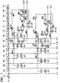
- FIG. 1 is a diagram showing the configuration of an embodiment of a delay circuit according to the present invention.
- FIG. 2 is a timing diagram for illustrating the embodiment of the delay circuit according to the present invention.
- FIGS. 3A to C are timing diagrams for illustrating the operating mode of the DLL, where FIG. 3A shows a 1T mode, FIG. 3B shows a 2T mode and FIG. 3C shows a 1.5T mode.
- FIG. 4 is a diagram showing the configuration of an embodiment of the DLL according to the present invention.
- FIG. 5 is a diagram showing the configuration of an embodiment of a delay line circuit (CDL) according to the present invention.
- FIG. 6 is a diagram showing the configuration of another embodiment of a delay line circuit (CDL) according to the present invention.
- CDL delay line circuit
- FIG. 7 is a diagram showing the configuration of still another embodiment of a delay line circuit (CDL) according to the present invention.
- CDL delay line circuit
- FIG. 8 is a diagram showing the configuration of a second embodiment of the DLL according to the present invention.
- FIG. 9 is a diagram showing the configuration of a selector in the second embodiment of the DLL according to the present invention.
- FIG. 10 is a diagram showing the configuration a multiplexer in the second embodiment of the DLL according to the present invention.
- FIG. 11 is a diagram showing the configuration of a mode decision circuit in the second embodiment of the DLL according to the present invention.
- FIG. 12 is a timing diagram for illustrating the operation of the 1T mode in the second embodiment of the DLL according to the present invention.
- FIG. 13 is a timing diagram for illustrating the operation of the 1.5T mode in the second embodiment of the DLL according to the present invention.
- FIG. 14 is a diagram showing the configuration of a third embodiment of the DLL according to the present invention.
- FIG. 15 is a diagram showing the configuration of a selector in the third embodiment of the DLL according to the present invention.
- FIG. 16 is a diagram showing the configuration of a duty ratio detection circuit in the third embodiment of the DLL according to the present invention.
- FIG. 17 is a diagram showing the configuration of a fourth embodiment of the DLL of the present invention.
- FIG. 18 is a diagram showing the configuration of a fifth embodiment of the DLL of the present invention.
- FIG. 19 is a diagram showing the configuration of a phase detector in the fifth embodiment of the DLL of the present invention.
- FIG. 20 is a diagram showing the configuration of a dummy circuit (BUF-SW) in the fifth embodiment of the DLL of the present invention.
- FIG. 21 is a diagram showing the configuration of a conventional DLL (synchronous delay loop).
- FIG. 22 is a diagram showing the configuration of the conventional DLL.
- FIG. 23 is a diagram showing the configuration of a conventional delay line circuit.
- the present invention comprises a delay line circuit in which the propagation path for the rising edge and that for the falling edge of an input signal are independently selected to provide for a variable duty ratio.
- a delay circuit includes a first delay line circuit having a plurality of stages of delay units (inverters 101 , 102 , 103 , . . . , 110 , . . . ), a second delay line circuit having a plurality of stages of delay units (NANDS 111 , 112 , 113 , . . . , 110 , . . . ), and a plurality of transfer circuits ( 131 , 132 , 133 , . . . , 141 , . . . ) provided in association with respective stages of the delay units of the first delay line circuit.
- the transfer circuits performs control as to whether or not the transfer of the outputs (I 1 , I 2 , I 3 , . . . ) of the output delay units is to be made to associated stages of the delay units of the second delay line circuit.
- the delay units ( 111 , 112 , 113 , . . . ) of the respective stages of the second delay line circuit receive outputs of the transfer circuits ( 131 , 132 , 133 , . . . ) provided in association with respective stages of the delay units and outputs (O 1 , O 2 , O 3 , O 4 , . . . ) of the delay units ( 112 , 113 , 114 , 115 . . . ) preceding to the delay units in question to send output signals to the following stage delay unit or output ends (O 0 ).
- One of a plurality of the transfer circuits ( 131 , 133 , 135 , 137 , . . . ), which respectively receive outputs (I 0 , I 2 , I 4 , I 6 , . . . ) of even-numbered stages of delay units of the first delay line circuit, is selected by a control signal (R_ 2 , R_ 6 , R_ 10 , . . . ) associated with the transfer circuit.
- One of a plurality of transfer circuits ( 132 , 134 , 136 , 138 , . . . ), which respectively receive outputs (I 1 , I 3 , I 5 , I 7 , . . .
- the rise timing and the fall timing of an output signal O 1 of the second delay line circuit are variably set with respect to the rising and fall of the signal I 0 supplied to the first delay line circuit.
- the code of the set of control signals, supplied to the transfer circuits of the even-numbered and odd-numbered stages is preferably the thermometer code.
- a modified embodiment of the present invention at least includes a delay circuit, having a plural number of stages of delay units, such as 111 to 115 of FIG. 7 , a first switch which receives a selection control signal and is controlled to be on or off, such as N 12 of FIG. 7 , and a second switch, such as N 11 of FIG. 7 , which is connected to an output of a delay unit of the stage number in the delay units of the delay circuit, corresponding to the aforementioned selection control signal, and which is turned on at a time point one of the rise and falling edges of the input signal, supplied to and propagated through the delay circuit, has traversed the number of stages corresponding to the selection control signal, to set a common node, such as MFE 11 of FIG.
- the modified embodiment of the present invention also includes a signal generating circuit, which is composed by such as transistors P 21 , P 22 and an inverter INV 7 of FIG. 7 , and generates a rise or falling edge signal responsive to transition of the common node from the first logic value to the second logic value, and a control circuit composed by such as AND 2 , inverter INV 8 and transistor P 25 of FIG. 7 , which sets the common node to the original first logic value responsive to the other of the rise and falling edges of the input signal supplied to the delay circuit.
- a signal generating circuit which is composed by such as transistors P 21 , P 22 and an inverter INV 7 of FIG. 7 , and generates a rise or falling edge signal responsive to transition of the common node from the first logic value to the second logic value
- a control circuit composed by such as AND 2 , inverter INV 8 and transistor P 25 of FIG. 7 , which sets the common node to the original first logic value responsive to the other of the rise and falling edges of the input signal
- the delay circuit it is also possible for the delay circuit to have such a circuit configuration in which the delay units of the delay circuit are constituted by inverters, the second set of switches and the first set of the switches are connected common to the common nodes for odd-numbered stages (MFE 11 and MFO 11 ), for the outputs of the delay units of the odd-numbered stages, the second set of switches and the first set of the switches are connected common to the common nodes for even-numbered stages (MRE 11 and MRO 11 ), for the outputs of the delay units of the even-numbered stages, and delay of the rise and fall timing of the output are variably adjusted from the rise and fall timing of the input.
- MFE 11 and MFO 11 common nodes for odd-numbered stages
- MRE 11 and MRO 11 the common nodes for even-numbered stages
- delay of the rise and fall timing of the output are variably adjusted from the rise and fall timing of the input.
- a delay synchronous loop (DLL) device includes a variable delay circuit ( 10 ) which receives an input signal and which variably delays the rise and fall timing of the input signal to output the resultant signal, a multiplexing circuit ( 92 ) for outputting an output signal the pulse width of which is prescribed by the rise and fall of the signal delayed by the variable delay circuit 10 , and a control circuit ( 12 and 13 ) for comparing the rise phase and the fall phase of the input signal with the rise phase and the fall phase of the output signal to variably control the delay time of the variable delay circuit based on the result of the phase comparison.
- the multiplexing circuit ( 92 ) includes a circuit for switching between the decision of the rise timing and the fall timing of the output signal based on the rise and the fall of the signal output from the variable delay circuit and the decision of the rise timing and the fall timing of the output signal based on the fall and the rise of the signal output from the variable delay circuit, in accordance with the input mode decision signal.
- the control circuit varies the rise timing and the fall timing of the output signal in the variable delay circuit ( 10 ), based on the result of phase comparison of the rise of the input signal and the rise of the output signal CLK_FDB and between the rise of the input clock signal and the rise of the output signal, or varies the fall timing and the rise timing of the output signal in the variable delay circuit ( 10 ), based on the result of phase comparison of the rise of the input signal and the rise of the output signal CLK_FDB and between the fall of the input signal and the fall of the output signal.
- the present embodiment includes a mode decision circuit 91 for checking the operating mode, based on the result of phase comparison output from the phase detector, determining the value of the mode decision signal and outputting the so determined signal value.
- a mode decision circuit 91 for checking the operating mode, based on the result of phase comparison output from the phase detector, determining the value of the mode decision signal and outputting the so determined signal value.
- a duty ratio detection circuit ( 93 ) for detecting the duty ratio of the feedback clock signal CLK_FDB in the DLL to output a duty ratio detection signal.
- the multiplexing circuit ( 92 ) switches between the decision of the rise timing and the fall timing of the output signal based on the rise and the fall of the signal output from the variable delay circuit ( 10 ), and the decision of the fall timing and the rise timing based on the fall and the rise of the signal output from the variable delay circuit, in accordance with the input mode decision signal M_SEL controlling the operating mode.
- the control circuit may also include a selector circuit ( 90 a ) for selecting two of the first result of phase comparison PD_R 0 of the rise of the input clock signal CLK and the rise of the feedback clock signal CLK_FDB in the first phase detector ( 12 1 ), second result of phase comparison PD_F 0 of the fall of the input clock signal CLK and the fall of the feedback clock signal CLK_FDB in the second phase detector ( 12 2 ) and the duty ratio detection enable signal, based on a duty ratio detection enable signal DCCen and the mode decision signal M_SEL, to vary the delay value of the rise timing and the fall timing of the output signal in the variable delay circuit ( 10 ).
- a selector circuit 90 a ) for selecting two of the first result of phase comparison PD_R 0 of the rise of the input clock signal CLK and the rise of the feedback clock signal CLK_FDB in the first phase detector ( 12 1 ), second result of phase comparison PD_F 0 of the fall of the input clock signal CLK and the fall of the feedback
- the selector ( 90 a ) varies the delay value of the rise timing and the fall timing of the output signal in the variable delay circuit ( 10 ), in accordance with the first result of phase comparison PD_R 0 and the second result of phase comparison PD_F 0 , or varies the delay value of the rise timing and the fall timing of the output signal in the variable delay circuit ( 10 ), in accordance with the second result of phase comparison PD_R 0 and the first result of phase comparison PD_F 0 , based on the mode decision signal M_SEL.
- the selector ( 90 a ) varies the delay value of the rise timing and the fall timing of the output signal in the variable delay circuit ( 10 ), in accordance with the first result of phase comparison PD_R 0 and PD_DCC, or varies the delay value of the rise timing and the fall timing of the output signal in the variable delay circuit ( 10 ), in accordance with the PD_DCC and PD_R 0 , based on the mode decision signal M_SEL.
- a further embodiment of the present invention shown in FIG. 18 , includes a first delay circuit ( 10 1 ) having a variable delay time and outputting a signal corresponding to an input clock signal the rising of which has been delayed, a second delay circuit ( 10 2 ) having a variable delay time and outputting a signal corresponding to an input clock signal the falling of which has been delayed, a third delay circuit ( 15 1 ) receiving an output signal of the first delay circuit ( 10 1 ) and finely adjusting the phase of the signal to output the resultant signal, a fourth delay circuit ( 15 2 ) receiving an output signal of the second delay circuit ( 10 2 ) and finely adjusting the phase of the signal to output the resultant signal.
- the further embodiment also includes a multiplexing circuit ( 92 ) receiving and multiplexing an output signal of the third delay circuit and an output signal of the fourth delay circuit to output a sole output clock signal, in which the multiplexing circuit outputs, in accordance with an input mode decision signal M_SEL, an output clock signal CLK_ 0 , the rise timing and the fall timing of which are prescribed based on the rising and the fall of the input clock signal, respectively, or an output clock signal CLK_ 0 , the fall timing and the rise timing of which are prescribed based on the rising and the fall of the input clock signal, respectively.
- the present modification also includes a dummy circuit ( 95 ) for delay adjustment, for generating a feedback clock signal CLK_FDB in phase with the output clock signal and a feedback clock signal CLK_FDB antiphase to the output clock signal, based on the transition of the output clock signal CLK_ 0 , and for selecting one of the feedback clock signals as the feedback clock signal CLK_FDB, based on the mode decision signal, a first phase detector ( 94 1 ) for comparing the phase of the rising edges of the input clock CLK and the feedback clock signal CLK_FDB to output a non-inverted result of phase comparison and an inverted result of phase comparison to output one of the non-inverted result of phase comparison and the inverted result of phase comparison as the first result of phase comparison PD_R 0 based on the mode decision signal, a second phase detector ( 94 2 ) for comparing the phase of the falling edges of the input clock signal and the feedback clock signal to output a non-inverted result of phase comparison and an inverted result of phase comparison to output one
- FIG. 1 shows a structure of a delay circuit embodying the present invention.
- I 0 and O 0 denote an input and an output, respectively, while R_ 2 , R_ 6 , R_ 10 , R_ 14 and R_ 18 are rise control signals and F_ 4 , F_ 8 , F_ 12 , F_ 16 and F_ 20 are fall control signals.
- the delay circuit of the present embodiment includes a first delay line circuit, composed of plural cascaded inverters 101 , 102 , . . . , and 110 , a second delay line circuit, composed of plural cascaded NAND circuits 111 , 112 , 113 , . . . , and 121 , and a set of transfer circuits, composed of plural NAND circuits 131 to 141 .
- the NAND circuits 131 , 133 , 135 , 137 , . . . have first input ends connected to even-numbered stage inputs I 0 , I 2 , I 4 , I 6 , . . . , of the first delay line circuit, respectively, while having second input ends connected to the rise control signals R_ 2 , R_ 6 , R_ 10 , R_ 14 , . . . , respectively, and having output ends connected to first input ends of the NAND circuits 111 , 113 , 115 , 117 , . . . of the second delay line circuit respectively.
- the second input ends of the NAND circuits 111 , 113 , 115 , 117 , . . . of the second delay line circuit are connected to outputs O 1 , O 3 , O 5 , O 7 , . . . of the preceding stage NAND circuits 112 , 114 , 116 , 118 , . . . , respectively.
- the NAND circuits 132 , 134 , 136 , 138 , . . . have first input ends connected to odd-numbered stage outputs I 1 , I 3 , I 5 , I 7 , . . . , of the first delay line circuit, respectively, while having second input ends connected to the fall control signals F_ 4 , F_ 8 , F_ 12 , F_ 16 , . . . , and having output ends connected to first input ends of the NAND circuits 112 , 114 , 116 , 118 , . . . of the second delay line circuit respectively.
- the outputs O 0 to O 10 of the respective delay units of the second delay line circuit are set to the rise timing and the fall timing shown in FIG. 2 .
- the numbers affixed to the rising and falling edges of the operating waveform of FIG. 2 denote the numbers of stages of the gates as from the rise and fall of the input I 0 (the number of gates of the first delay line circuit, transfer circuit and the second delay line circuit).
- a rising edge supplied from the input I 0 , is inverted by the inverter 101 and becomes the falling edge (see fall ‘1’ of I 1 of FIG. 2 ), and is further inverted by the inverter 102 to become a rising edge.
- the control signal R_ 6 is High
- the NAND circuit 133 is responsive to rising transition of the node I 2 from Low to High to change its output from High to Low.
- the output O 2 of the NAND circuit 113 forming the delay unit of the second delay line circuit, is responsive thereto and goes High from Low. That is, the output O 2 rises with a delay of four delay time units as from the rising edge of the input I 0 (see rise of O 2 of FIG. 2 ‘4’).
- An output of the NAND circuit 132 which receives the control signal F_ 4 of Low level, is High, such that the output O 1 of the NAND circuit 112 undergoes a transition from High to Low responsive to the transition of the output O 2 from Low to High.
- the output O 1 falls with a delay of five delay time units as from the rising edge of the input I 0 (see fall of O 1 of FIG. 2 ‘5’).
- An output of the NAND circuit 131 which receives the control signal R_ 2 of Low level, is High, such that the output O 0 of the NAND circuit 111 undergoes a transition from Low to High responsive to the transition of the output O 1 from High to Low.
- the output O 0 rises with a delay of six delay time units as from the rising edge of the input I 0 (see fall of O 0 of FIG. 2 ‘6’).
- the rising edge supplied from the input I 0 to the first delay line circuit is sent to the output O 0 with a delay of the sum of the delay time (2 ⁇ td) for two stages of the delay elements (inverters) of the first delay line circuit, the delay time (td) of the transfer circuit 133 at the signal turning point and the delay time (3 ⁇ td) for three stages of the delay elements (NANDs) of the second delay line circuit.
- the NAND circuit 135 which receives the signal as input, has its output transferred from High to Low, responsive to rising transition from Low to High of the input I 4 , such that the output O 4 of the NAND circuit 115 transfers from Low to High.
- the output 4 rises with a delay of six delay time units as from the rising edge of the input I 0 (see rise of O 4 of FIG. 2 ‘6’).
- the output of the NAND circuit 134 is High.
- the NAND circuit 114 is responsive to rising transition of the output O 4 to cause transition of the output O 3 from High to Low. That is, the output O 3 falls with a delay of seven time units from the rising edge of the input I 0 (see fall of O 3 of FIG. 2 ‘7’).
- the outputs O 6 , O 8 and O 10 of the second delay line circuit rise with a delay of 8, 10 and 12 delay time units as from the rising edge of the input I 0
- the outputs O 5 , O 7 and O 9 of the second delay line circuit rise with a delay of 9, 11 and 13 delay time units as from the rising edge of the input I 0 (see FIG. 2 ).
- the falling edge supplied from the input I 0 (see fall of I 0 of FIG. 2 ‘0’) is inverted by the inverter 101 to become a rising edge (see rising of I 1 of FIG. 2 ‘1’).
- the rising edge is further inverted by the inverters 102 to 107 to become a rising edge at I 7 .
- the NAND circuit 138 Since the control signal F_ 16 is High, the NAND circuit 138 , supplied with the output I 7 , as input, is responsive to the rising transition of the output I 7 from the Low level to the High level, and causes the transition of the output from the High level to the Low level.
- the output O 7 of the NAND circuit 118 transfers from the Low level to the High level.
- the output O 7 rises with a delay of 9 delay time units from the falling edge of the input I 0 (see rising of O 7 of FIG. 2 ‘9’).
- the NAND circuit 137 Since the control signal R_ 14 is High, the NAND circuit 137 , supplied with the output I 6 , as input, is responsive to the falling transition of the output I 6 from the High level to the Low level, to cause the transition of the output from the Low level to the High level.
- the output O 6 of the NAND circuit 116 is responsive to transition of the output O 7 from the Low level to the High level to transfer from the High level to the Low level.
- the output O 6 falls to a Low level with a delay of ten delay time units from the falling edge of the input I 0 (see falling of O 6 of FIG. 2 ‘10’).
- the output of the NAND circuit 136 supplied with the output I 5 , as input, is Low 1 , such that the output O 5 of the NAND circuit 116 is responsive to transition of the output O 6 from the High level to the Low level to transfer from the Low level to the High level. That is, the output O 5 rises to a High level with a delay of 11 delay time units from the falling edge of the input I 0 (see falling of O 5 of FIG. 2 ‘11’).
- the NAND circuit 135 Since the control signal R_ 10 is High, the NAND circuit 135 , supplied with the output I 4 , as input, is responsive to the falling transition of the output I 4 from the High level to the Low level, to cause the transition of the output from the Low level to the High level.
- the output O 4 of the NAND circuit 115 transfers from the High level to the Low level responsive-to transition of the output O 5 from the Low level to the High level,.
- the output O 4 falls to a Low level with a delay of 12 delay time units from the falling edge of the input I 0 (see falling of O 4 of FIG. 2 ‘12’).
- the outputs O 3 and O 1 rise to a High level with a delay of 13 and 15 delay time units from the falling edge of the input I 0 .
- the outputs O 2 and O 0 fall to a Low level with a delay of 14 and 16 delay time units as from the falling edge of the input I 0 , respectively.
- the falling edge supplied from the input I 0 to the first delay line circuit is sent to the output O 0 with a delay of the sum of the delay time (7 ⁇ td) for seven stages of the delay elements (inverters) of the first delay line circuit, the delay time (td) of the transfer circuit 139 at the signal turning point and the delay time (8 ⁇ td) for eight stages of the delay elements (NANDs) of the second delay line circuit, that is, with a delay of 16 delay time units (16 ⁇ td).
- the NAND circuit 140 Since the control signal F_ 20 is High, the NAND circuit 140 , supplied with the output I 9 , as input, is responsive to the transition of the output I 9 from the Low level to the High level, to cause the transition of the output from the High level to the Low level.
- the output O 9 of the NAND circuit 120 transfers from the Low level to the High level.
- the output O 9 rises with a delay of 11 delay time units from the falling edge of the input I 0 (see rising of O 9 of FIG. 2 ‘11’).
- the NAND circuit 139 Since the control signal R_ 18 is High, the NAND circuit 139 , supplied with the output I 8 , as input, is responsive to the transition of the output I 8 from the High level to the Low level, to cause the transition of the output from the Low level to the High level.
- the output O 9 of the NAND circuit 119 is responsive to transition of the output O 9 from the Low level to the High level to cause transition of the output O 8 from the High level to the Low level. That is, the output O 8 falls to the Low level with a delay of 12 delay time units from the falling edge of the input I 0 (see rising of O 8 of FIG. 2 ‘12’).
- the NAND circuit 141 Since the control signal R_ 22 is High, the NAND circuit 141 , supplied with the output I 10 , as input, is responsive to the transition of the output I 10 from the High level to the Low level, to cause the transition of the output from the Low level to the High level.
- the output O 6 of the NAND circuit 116 is responsive to transition of the output O 7 from the Low level to the High level, transfers from the High level to the Low level.
- the NAND circuit 121 receives an output of the NAND circuit 141 and O 11 (fixed potential: High level) as inputs and, responsive to the falling of the output of the NAND circuit 141 , causes the output O 10 to fall from a High level to a Low level with a delay of 12 delay time units from the falling edge of the input I 0 (see falling of O 10 of FIG. 2 ‘12’).
- an output signal from O 1 is such a signal in which the rising edge thereof is delayed by 6 delay time units from the rising of the input I 0 and in which the falling edge thereof is delayed by 16 delay time units from the fall of the input I 0 .
- the delay time as from the rising of the input I 0 until the rising of the signal from the output O 0 and the delay time as from the fall of the input I 0 until the fall of the signal from the output O 0 may be varied independently of each other. That is, the pulse width and hence the duty ratio may be varied. Meanwhile, the number of stages of the delay units in the first and second delay line circuits is arbitrary.
- the delay circuit shown in FIG. 1 , realizes the 1.5T mode, by a simplified structure, and may be conveniently used in the DLL.
- FIG. 4 shows an illustrative structure of the DLL employing a delay circuit of the present embodiment.
- the DLL includes a first delay circuit 10 A (CDL) which receives an input clock signal and which has variable delays of the rising edge and the falling edge of an output signal, a second delay circuit 15 1 (FDL) which receives rising edges (O 0 _R and E 0 _R) of clock signals output from the first delay circuit 10 A (CDL) to make fine adjustment of the output signal, and a third delay circuit 15 2 (FDL) which receives falling edges (O 0 _F and E 0 _F) of clock signals output from the first delay circuit 10 A (CDL) to make fine adjustment of the output signal.
- CDL first delay circuit 10 A
- FDL second delay circuit 15 1
- FDL third delay circuit 15 2
- the DLL also includes a multiplexer 16 (MUX) which receives and multiplexes an output signal of the second delay circuit 15 1 and an output signal of the third delay circuit 15 2 and a multiplexer 17 (data multiplexer) which receives a clock signal CLK_ 0 from the multiplexer 16 (MUX) and converts read data input in parallel into serial data in synchronization with the rise and fall of the clock signal to output the resulting serial data to a data output terminal DQ.
- the reference numeral 17 denotes a data output path made up e.g. by a data multiplexer and an output buffer.
- the DLL also includes a dummy circuit 18 (dummy multiplexer) having a delay time equivalent to the delay time of the multiplexer 17 , a first phase detector PD(R) 12 1 which receives an input clock signal CLK and an output of the dummy circuit 18 and detects the phase difference of the rising edges of the two input signals, and a second phase detector PD(R) 12 2 which receives an input clock signal CLK and an output of the dummy circuit 18 and detects the phase difference of the falling edges of the two input signals.
- a dummy circuit 18 dummy multiplexer
- the DLL also includes a first counter 13 1 for performing up/down counting of the result of phase comparison (UP/DOWN) output from the first phase detector 12 1 PD(R), a second counter 13 2 for performing up/down counting of the result of phase comparison (UP/DOWN) output from the second phase detector 12 2 PD(R), a first selection circuit 14 1 SEL(R) for outputting a control signal for adjusting the rise timing in the first selection circuit 10 A based on a count output of the first counter 13 1 and a second selection circuit 14 2 SEL(F) for outputting a control signal for adjusting the fall timing in the first selection circuit 10 A based on a count output of the second counter 13 2 .
- the second delay circuit 15 1 may be composed by a known type of a phase interpolator for outputting an output signal of a phase corresponding to the division of a phase difference between rising edges of two signals (O 0 -R, E 0 -R).
- the third delay circuit 15 2 may be composed by a known type of a phase interpolator for outputting an output signal of a phase corresponding to the division of a phase difference between falling edges of two signals (O 0 -F, E 0 -F).
- a structure of the FDL see e.g. FIG. 1 of the aforementioned Patent Publication 1. It is noted that a dummy circuit of a delay time equivalent to the delay of the input buffer 11 may be provided between the dummy circuit 18 and the inputs of the phase detectors 12 1 and 12 2 .
- the first delay circuit 10 A (R/F) is composed by a delay circuit of the embodiment shown in FIG. 1 .
- the propagation paths of the input I 0 ⁇ output O 0 of the rising edges and the falling edges of the input I 0 expressed by the number of gate stages from the rise and fall of the input I 0 , in the operating waveform of FIG. 2 , are of 6 and 16 stages, respectively. That is, the duty ratio can be variably set by varying the selected control signal.
- a data output from the data output terminal DQ by the rising edge of the clock signal CLK may be synchronized with the fall of the clock signal of the next cycle, while a data output from the data output terminal DQ by the falling edge of the clock signal CLK may be synchronized with the rise of the clock signal of the next cycle.
- the 1.5T mode of FIG. 3C may be realized with the sole delay circuit 10 A. Meanwhile, not only the 1.5T mode but also x.5, where x is a number such that x>0, may also be realized in the present embodiment.
- two second delay line circuits of FIG. 1 are connected to the first delay line circuit made up by inverters 101 to 110 , as shown in FIG. 5 .
- the present embodiment includes, as shown in FIG.
- a first delay line circuit ( 101 to 110 ), having plural stages of the delay units (inverters), a first group of transfer circuits ( 121 to 129 ), a second delay line circuit ( 111 to 119 ) composed of plural delay units (NAND circuits), a second group of transfer circuits ( 141 to 147 ), and a third delay circuit ( 131 to 137 ) composed of plural delay units (NAND circuits).
- the number of stages of the delay unit in the respective delay circuits is arbitrary.
- the first group of transfer circuits ( 121 to 129 ) and the second group of transfer circuits ( 141 to 147 ) are alternately supplied with a fall control signal (F_J) and with a rise control signal (R_I), as in the circuit shown in FIG. 1 .
- the second delay line circuit and the third delay circuit output signals (O 0 _R, O 0 _F and E 0 _R, E 0 _F) which rise and fall with a delay of gate stages prescribed by the selected control signal from the rising edge and the falling edge from the input IO.
- the delay circuit of FIG. 5 is applied to the delay circuit 10 A shown in FIG.
- the structure shown in FIG. 5 is effective to simplify and reduce the size of the circuit.
- the duty cycle may be made variable.
- the 1.5T mode may be realized to reduce the jitter without substantially increasing the area of the DLL delay circuit or the operating current.
- the circuit block surrounded by a broken line in FIG. 5 two inverters of the first delay line circuit, two NANDs of the associated second and third delay circuits and two transfer circuits of each of the first and second groups of the transfer circuits) are made up by 36 transistors.
- FIG. 6 shows the circuit configuration according to a further embodiment of the present invention.
- the NAND circuits 131 to 141 of the first group of transfer circuits of FIG. 1 are composed by NOR circuits 171 to 181 and the NAND circuits 111 to 121 of the second group of transfer circuits are composed by NOR circuits 151 to 161 .
- the rise control signals /R_ 2 , /R_ 6 , /R_ 10 , /R_ 14 and /R_ 18 and the fall control signals /F_ 4 , /F_ 8 , /F_ 12 , /F_ 16 and /F_ 20 are all active at a Low level.
- the operation of the delay circuit, shown in FIG. 6 is basically the same as that shown in FIG. 1 .
- FIG. 7 shows the configuration of the other embodiment of a coarse delay line (CDL) according to the present invention.
- the coarse delay line (CDL) includes a multiplexer which receives signals of preset inverter stages of the delay circuit composed of a plural number of inverter delay element stages and which selects an edge at a selected inverter stage number of the inverter stages, out of the edges propagated in the delay circuit, based on the input selection control signal, to output the so selected edge.
- the rise control signals /R_ 5 , /R_ 7 , /R_ 9 , /R_ 11 , . . . and the fall control signals /F_ 4 , /F_ 6 , /F_ 8 and /F_ 10 , forming selection control signals for the multiplexer, are formed by binary codes. From the outputs of the odd inverter stages 11 , 13 , 15 , 17 , . . .
- the delay circuit CDL includes a sole delay circuit having plural stages of inverter files 101 to 105 .
- a Nch transistor N 11 which has a gate connected to an output I 1 of the delay circuit and which is controlled to be turned on or off, and a Nch transistor N 12 which has a gate supplied with a control signal F_ 4 and which is controlled to be turned on or off, are connected in series across the ground and a common node MFE 11 , whilst a Nch transistor 51 which has a gate connected to the input I 5 and which is controlled to be turned on or off, and a Nch transistor N 52 which has a gate supplied with the control signal F_ 8 and which is controlled to be turned on or off, are connected in series across the ground and the common node MFE 11 .
- Pch transistor P 22 which has a source connected to the power supply via Pch transistor P 21 in the on-state, and has a gate connected to the common node MFE 11 .
- the Pch transistor P 22 has a drain connected to a common node MFE 2 , and an inverter INV 7 which has an input connected to the common node MFE 2 and outputs an even falling signal E 0 _F.
- Pch transistor P 24 which has a source connected to the power supply via Pch transistor P 23 in the on-state and has a gate connected to the common node MFO 11 .
- the Pch transistor P 24 has a drain connected to the common node MFO 2 , and an inverter INV 6 which has an input connected to the common node MFO 2 and outputs an odd falling signal O 0 _F.
- AND 2 a second AND circuit having inputs connected to outputs of inverters INV 6 , INV 7 and the signal I 0 .
- Pch transistors P 25 and P 26 are provided between the power supply and the common nodes MFE 11 and MFO 11 .
- An output of the AND 2 is inverted by an inverter INV 8 and supplied to the gates of the Nch transistors N 3 and N 4 .
- Nch transistors N 3 and N 4 across the common node MFE 2 and the ground and across the common node MFO 2 and the ground, respectively.
- An output of the AND 2 is supplied to the gates of the Nch transistors N 3 and N 4 .
- a Nch transistor 21 which has a gate connected to an even number stage output I 2 of the delay circuit and which is controlled to be on or off, is connected in series across the ground and the common node MRE 11 , whilst a Nch transistor 61 which has a gate connected to the input I 6 and which is controlled to be on or off, and a Nch transistor 62 which has a gate supplied with the control signal R_ 9 and which is controlled to be on or off, are connected in series across the ground and the common node MRE 11 .
- a Pch transistor P 12 which has a source connected to the power supply via Pch transistor P 11 in the on state and having a gate connected to the common node MRE 11 .
- the drain of the Pch transistor P 12 is connected to the common node MRE 2 .
- An even rising signal E 0 _R is output from an inverter INV 5 , inverting the output of an inverter INV 2 which has an input connected to the common node MRE 2 .
- a Pch transistor P 14 which has a source connected to the power supply via Pch transistor P 13 in the on-state, and also has a gate connected to the common node MRO 11 .
- the drain of the Pch transistor P 14 is connected to the common node MRO 2 , and an odd rising signal O 0 _R is output from an inverter INV 5 which inverts an output of an inverter INV 1 which has an input connected to the common node MRO 2 t.
- AND 1 a first AND circuit having inputs connected to outputs of the inverters INV 1 and INV 2 and the input I 0 .
- Pch transistors P 15 and P 16 across the power supply and the common nodes MRE 11 and MRO 11 .
- An output of the AND 1 is inverted by inverter INV 3 and supplied to the gates of the Pch transistors P 15 and P 16 .
- Nch transistors N 1 and N 2 across the common node MRE 2 and the ground and across the common node MRO 2 and the ground, respectively.
- An output of the AND 1 is supplied to the gates of the Nch transistors N 1 and N 2 .
- the structure downstream of the output I 9 of the delay circuit is such that connection is made via switch to the common nodes MFE 11 and MFO 11 via switch through a series circuit of transistors having gates connected to outputs of every fourth odd inverter stage and a transistor having a gate coupled to a control signal.
- the structure downstream of the output I 10 of the delay circuit is such that connection is made via switch to the common nodes MFE 11 and MFO 11 through a series circuit of transistors having gates connected to outputs of every four odd inverter stage and a transistor having a gate coupled to a control signal.
- the common node MFE 11 is discharged, at a time point when the falling edge is propagated through 7 inverter stages 101 to 107 in the delay circuit, through the Nch transistor N 71 , the gate of which is supplied with the falling edge of the output I 7 , and the Nch transistor N 72 , the gate of which is supplied with the control signal F_ 10 in the High level.
- the duty ratio may be varied by varying the phase of the rise time.
- the rising phase and the fall phase of the output signal may be varied independently of each other to vary the duty ratio.
- the circuit structure for generating a signal supplied to the FDL of FIG. 4 is taken as an example for explanation. It is noted that each one of the rising edges and the falling edges may be selected. In such case, the circuit structure is such a one in which the signal E 0 _R and the signal EO_F, for example, are output.
- the 1.5T mode can be realized. That is, the above circuit helps reduce the current consumption as well as the chip area of the semiconductor memory devices, such as DDRII/I-SDRAM.
- the frequency can be changed instantaneously to realize frequency modulation.
- PLL source frequency synthesizer
- FIG. 8 shows the configuration of a further embodiment of the present invention.
- the components which are the same as those shown in FIG. 22 are indicated by the same reference numerals.
- the elements which are the same as those of the conventional DLL circuit shown in FIG. 22 are not explained here in order to avoid redundancy.
- a first phase detector P/D(R) 12 1 compares the phase of the rising edge of the input clock signal CLK with the phase of the rising edge of the feedback clock signal CLK_FDB of the DLL circuit, also termed ‘internal clock signal’, and outputs a first phase comparison result signal PD_R 0 to a selector 90 .
- a second first phase detector P/D(F) 12 2 compares the phase of the falling edge of the input clock signal CLK with the phase of the falling edge of the feedback clock signal CLK_FDB, and outputs a second phase comparison result signal PD_F 0 to the selector 90 .
- the selector 90 receives a mode decision signal M_SEL, output from a mode decision circuit 91 , as a switching control signal, and determines to which of first and second counters 13 1 and 13 2 the first phase comparison result signal PD_R 0 is to be supplied.
- the selector 90 also manages control to send the second phase comparison result signal PD_F 0 to the counter different from the counter supplied with the first phase comparison result signal PD_R 0 .
- the mode decision circuit 91 takes in the first phase comparison result signal PD_R 0 and/or the second phase comparison result signal PD_F 0 , based on an input mode latch signal LAT, and decides on the operating mode, based on one or the combination of the two signals, to output the mode decision signal M_SEL
- the 1.5T mode and 1T mode are realized when the mode decision signal M_SEL is High and Low, respectively.
- the first CDL 15 1 delays the rising edge of the clock signal, output from the buffer 11 , by delay time determined by the control signal, and outputs a pair of signals O 0 _R and E 0 _R rising with different phase for the duration of unit phases, such as, foe example, for two inverter stages.
- the second CDL 15 2 delays the falling edge of the clock signal, output from the buffer 11 , by delay time determined by the control signal, and outputs a pair of signals O 0 _F and E 0 _F rising with different phase for the duration of unit phases, such as, for example, for two inverter stages.
- a multiplexer circuit 92 includes a multiplexer, not shown, and a selection circuit, also not shown, for multiplexing a signal CLK_R output from the first CDL 15 1 and a signal CLK_F output from the second CDL 15 2 , to a sole clock signal.
- the selection circuit manages control to switch between input signal edges, prescribing the rising edge and the falling edge of the clock signal CLK_ 0 , based on the input mode decision signal M_SEL.
- the rise timing of the clock signal CLK_ 0 is determined by the transition of one of the signals CLK_R and CLK_ 0 , as selected by the selection circuit, based on the mode decision signal M_SEL, while the fall timing of the clock signal CLK_ 0 is determined by the transition of the other of the signals CLK_R and CLK_ 0 .
- a configuration of the selector 90 , multiplexer circuit 92 and the mode decision circuit 91 of FIG. 9 is hereinafter explained.
- FIG. 9 shows an illustrative structure of the selector 90 including multiplexers 901 and 902 each having first and second input terminals for receiving the first phase comparison result signal PD_R 0 and the second phase comparison result signal PD_F 0 .
- the multiplexer 901 selects and outputs the first phase comparison result signal PD_R 0 , supplied to the first input terminal thereof, as an output signal PD_R, while the multiplexer 902 selects and outputs the second phase comparison result signal PD_F 0 , supplied to the second input terminal thereof, as an output signal PD_F.
- the multiplexer 901 selects and outputs the second phase comparison result signal PD_F 0 , supplied to the second input terminal thereof, as an output signal PD_R, while the multiplexer 902 selects and outputs the first phase comparison result signal PD_R 0 , supplied to the first input terminal thereof, as an output signal PD_F.
- FIG. 10 shows the configuration of the multiplexer circuit 92 .
- the multiplexer circuit 92 includes two multiplexers 921 and 922 , each including first and second input terminals for receiving the signal CLK_R output from the first CDL 15 1 d and the signal CLK_F output from the first CDL 15 2 , and an SR flip-flop 923 which has a set terminal connected to an output of the multiplexer 921 and a reset terminal connected to an output of the multiplexer 922 .
- the multiplexer 921 selects and outputs the signal CLK_R supplied to the first input terminal, while the multiplexer 922 selects and outputs the signal CLK_F supplied to the second input terminal.
- the SR flip-flop 923 is set by the rising edge of the output of the multiplexer 921 to provide for the High level of the output CLK_ 0 , while being reset by the rising edge of the output of the multiplexer 922 to provide for the Low level of the output CLK_ 0 .
- the multiplexer circuit 92 outputs a clock pulse signal CLK_ 0 having the rise and fall prescribed by the rise of the signals CLK_R and CLK_F.
- the multiplexer 921 selects and outputs the signal CLK_F, input to the second input terminal thereof, while the multiplexer 922 selects and outputs the signal CLK_R, input to the first input terminal thereof.
- the SR flip-flop 923 is set by the rising of the output from the multiplexer 921 (rising of the signal CLK_F) to provide for a High level of the signal CLK_ 0 , while being reset by the rising of the output from the multiplexer 922 (rising of the signal CLK_R) to provide for a Low level of the signal CLK_ 0 .
- the multiplexer circuit 92 outputs a clock signal CLK_ 0 , the rising and fall of which are prescribed by the rise of the signal CLK_F (a signal corresponding to the input clock signal CLK the fall of which has been delayed) and by the rise of the signal CLK_R (a signal corresponding to the input clock signal CLK the rise of which has been delayed).
- the multiplexer circuit 92 switches between a mode (1T mode) which, when the mode decision signal M_SEL is Low, generates the rising of the output signal CLK_ 0 from the rise of the CLK_R output from the first CDL 15 1 (hence from the rise of the input clock signal CLK), while generating the fall of the output signal CLK_ 0 from the rise of the signal CLK_F output from the second CDL 15 2 (hence from the fall of the input clock signal CLK), and a mode (1.5T mode) which, when the mode decision signal M_SEL is High, generates the fall of the output signal CLK_ 0 from the rise of the CLK_R output from the first CDL 15 1 (hence from the rise of the input clock signal CLK), while generating the fall of the output signal CLK_ 0 from the fall of the signal CLK_F output from the second CDL 15 2 (hence from the fall of the input clock signal CLK).
- a mode (1T mode) which, when the mode decision signal M_SEL is Low, generate
- FIG. 11 shows the configuration of the mode decision circuit 91 including a D type flip-flop 911 .
- the first phase comparison result signal PD_R 0 is sampled by the rise of a mode latch signal LAT and output as the mode decision signal M_SEL.
- a one-shot pulse generated by e.g. a power-on-reset circuit, provided outside of the DLL circuit, on power up of the device, or during the initializing operation, such as on resetting.
- FIGS. 12 and 13 are timing diagrams for illustrating the operation of the embodiment shown in FIG. 8 .
- FIG. 12 is a timing chart showing the operation when the mode decision signal M_SEL is Low. The operation corresponds to the 1T mode operation explained with reference to FIG. 3A .
- the 1T mode operation of the present embodiment is now explained with reference to FIGS. 12 and 8 .
- the clock signal CLK_FDB is generated with a delay proper to the circuit as from the clock signal CLK.
- the first phase detector 12 1 compares the phase of the rising edge of the clock signal CLK_FDB to the phase of the clock signal CLK and, if, with the first phase comparison result signal PD_R 0 , the phase of the clock signal CLK_FDB lags or leads the phase of the clock signal CLK, a High level and a Low level are output as the phase comparison result signal PD_R 0 , respectively.
- the mode latch signal LAT is output as a one-shot pulse.
- the mode decision circuit 91 latches the first phase comparison result signal PD_R 0 to output the mode decision signal M_SEL.
- the first phase comparison result signal PD_R 0 is Low when the mode latch signal LAT is output (when the one-shot pulse rises). That is, referring to FIG. 12 , the clock signal CLK_FDB, fed back to the first phase detector 12 1 rises ahead of the rise timing of the clock signal of the next cycle to cycle of the clock signal CLK with which the rising edge of the clock signal CLK_FDB was formed. Thus, the first phase detector 12 1 outputs the Low level as the first phase comparison result signal PD_R 0 .
- the mode decision circuit 91 which samples the first phase comparison result signal PD_R 0 with the rising edge of the mode latch signal LAT, outputs a Low level as the mode decision signal M_SEL to realize the 1T mode.
- the selector 90 outputs the first phase comparison result signal PD_R 0 and the second phase comparison result signal PD_F 0 to the first counter (R) 13 1 and to the second counter (R) 13 2 , respectively.
- a control signal from the first CDL(F) 10 1 has its delay value controlled so that the rising of the feedback clock signal CLK_FDB is in phase with the rising of the input clock signal CLK.
- a control signal from the second CDL(F) 10 2 has its delay value controlled so that the fall of the feedback clock signal CLK_FDB is in phase with the fall of the input clock signal CLK.
- the first FDL(F) 15 1 outputs an output signal CLK_R, with the finely adjusted rising phase, based on the phase difference between the rising edges of the two signals O 0 _R and E 0 _R, output from the first CDL(F) 10 1 .
- the second FDL(F) 15 2 outputs an output signal CLK_F, with the finely adjusted rising phase, based on the phase difference between the rising edges of the two signals O 0 _F and E 0 _F, output from the second CDL(F) 10 2 .
- the multiplexer circuit 92 performs switching control so that the rise timing of the clock signal CLK_R, delay-adjusted by the first FDL(F) 15 1 , will be used for the rising of the clock signal CLK_ 0 , and so that the rise timing of the clock signal CLK_F, delay-adjusted by the second FDL(F) 15 2 , will be used for the fall of the clock signal CLK_ 0 .
- the delay value is adjusted by the first CDL(F) 10 1 so that the falling edge of the feedback clock signal CLK_FDB, fed back to the phase detector 12 1 , will be coincident with the rising edge of e.g. the next cycle clock signal CLK in the 1T mode, and so that the falling edge of the feedback clock signal CLK_FDB will be coincident with the falling edge of e.g. the second next cycle clock signal CLK in the 1T mode.
- FIG. 13 is a timing chart illustrating the operation of the circuit of FIG. 8 in which the mode decision signal M_SEL is at a High level. This operation is the 1.5T operation explained with reference to FIG. 3C . The period of the clock signal CLK is shorter than that for the 1T mode shown in FIG. 12 . Referring to FIGS. 13 and 8 , the operation for the 1.5T mode in the present embodiment is explained.
- the mode latch signal LAT is output only once during e.g. the initializing operation of the DLL circuit.
- the mode decision circuit 91 latches the first phase comparison result signal PD_R 0 to output the mode decision signal M_SEL.
- the first phase comparison result signal PD_R 0 is in a High level during e.g. the initializing operation of the DLL circuit. That is, since the clock signal period is shorter, as shown in FIG. 13 , the feedback clock signal CLK_FDB, fed back to the phase detector 12 1 , rises with a lag as from the rising of the input clock signal CLK of the clock cycle next following the cycle of the input clock signal CLK by which the clock signal CLK_FDB was formed.
- the phase comparison result signal PD_R 0 is at a High level, and the mode decision circuit 91 outputs a High level as a mode decision signal M_SEL to set up the 1.5T mode.
- the selector 90 is switched so that the first phase comparison result signal PD_R 0 and the second phase comparison result signal PD_F 0 will be output to the second counter 13 2 and to the first counter 13 1 , based on the mode decision signal M_SEL of the High level, respectively.
- the CDL (R) 10 1 Based on the control signal, output from the first counter 13 1 (R), the CDL (R) 10 1 has its delay time controlled so that the fall of the feedback clock signal CLK_FDB will be in phase with the rise of the clock signal CLK. Based on the control signal, output from the first counter 13 1 (R), the CDL (F) 10 2 has its delay time controlled so that the rising of the feedback clock signal CLK_FDB will be in phase with the fall of the clock signal CLK.
- the first counter 13 1 (R) varies the delay time of the first CDL 10 1 (R), based on the second phase comparison result signal PD_F 0 from the second phase detector 12 2 , detecting the falling phase difference between the feedback clock signal CLK_FDB and the input clock signal CLK, while the second counter 13 2 (F) varies the delay time of the second CDL 102 (F), based on the first phase comparison result signal PD_R 0 from the first phase detector 12 1 , adapted for detecting the rising phase difference between the feedback clock signal CLK_FDB and the input clock signal CLK.
- the multiplexer circuit 92 generates the rising edge of the clock signal CLK_ 0 , using the clock signal CLK_F, delay-adjusted by the FDL 15 2 (F), while generating the falling edge of the clock signal CLK_ 0 , using the clock signal CLK_R, delay-adjusted by the first FDL 15 1 (R).
- the fall timing of the output clock signal CLK_ 0 is adjusted by the first CDL 10 1 , (R) and the first FDL 15 1 (R), while the rise timing of the output clock signal CLK_ 0 is adjusted by the second CDL 10 2 (F) and the second FDL 15 2 (R).
- the first CDL 10 1 (R) has a delay value set based on the output PD_F 0 of the second phase detector 12 2 (result of falling edge phase detection of the input clock signal CLK and the feedback clock signal CLK_FDB), while the second CDL 10 2 (F) has a delay value set based on the output PD_R 0 of the first phase detector 12 1 (result of rising edge phase detection of the input clock signal CLK and the feedback clock signal CLK_FDB).
- the delay length from the fall of the clock signal CLK until the rising of the feedback clock signal CLK_FDB may be shorter by one-half clock cycle, by the 1T mode, as shown in FIG. 13 , thereby reducing the delay variation caused by noise, that is, jitter.
- the mode decision circuit 91 shown in FIG. 11 , a mode decision is executed, using only the phase comparison result signal PD_R 0 , in order to realize the least functions.
- the mode decision circuit 91 is, of course, not limited to this configuration.
- the mode decision circuit 91 may be configured for latching the logical sum of the first phase comparison result signal PD_R 0 and the second phase comparison result signal PD_F 0 .
- the mode decision circuit 91 may be configured for executing the mode decision by carrying out preset logical calculations of the first phase comparison result signal PD_R 0 and the second phase comparison result signal PD_F 0 with other control signals.
- FIG. 14 shows the configuration of another embodiment of the DLL circuit according to the present invention.
- the present embodiment shown in FIG. 14 , includes a duty ratio detection circuit 93 (DCC), in addition to the structure of the embodiment shown in FIG. 8 .
- DCC duty ratio detection circuit 93
- the duty ratio detection circuit 93 receives the feedback clock signal CLK_FDB to detect the duty ratio to output a duty ratio detection signal PD_DCC to a selector 90 a.
- the selector 90 a is controlled by the mode decision signal M_SEL and by an input DCC enable signal DCCen, which validates the result of duty ratio detection, and selects two signals from the first phase comparison result signal PD_R 0 , second phase comparison result signal PD_F 0 and the detection signal PD_DCC, to transmit the selected signals to the first counter 13 1 (R) and the second counter 13 2 (F).
- FIG. 15 shows the configuration of the selector 90 a shown in FIG. 14 .
- the selector 90 a includes two multiplexers 901 , 902 , supplied at first and second input terminals thereof with the first and second phase comparison result signal PD_R 0 and PD_F 0 .
- the multiplexers 901 and 902 select and output PD_R 0 and PD_F 0 when the mode decision signal M_SEL is at a Low level.
- the selector 90 a further include an AND circuit 903 which receives the mode decision signal M_SEL and the DCC enable signal DCCen, an AND circuit 904 which receives an inverted version of the mode decision signal M_SEL and the DCC enable signal DCCen, a multiplexer 905 which has first and second input terminals supplied with an output of the multiplexer 901 and with the duty ratio detection signal PD_DCC, and a multiplexer 906 which has first and second input terminals supplied with an output of the multiplexer 902 and with the duty ratio detection signal PD_DCC.
- an AND circuit 903 which receives the mode decision signal M_SEL and the DCC enable signal DCCen
- an AND circuit 904 which receives an inverted version of the mode decision signal M_SEL and the DCC enable signal DCCen
- a multiplexer 905 which has first and second input terminals supplied with an output of the multiplexer 901 and with the duty ratio detection signal PD_DCC
- a multiplexer 906 which has first and second input
- FIG. 16 shows the configuration of the duty ratio detection circuit DCC 93 of FIG. 14 .
- the duty ratio detection circuit DCC 93 includes a charge pump circuit 931 and a comparator circuit 932 .
- the charge pump circuit 931 charges a capacitance, not shown (such as an internal node, e.g. a gate capacitance) during the High level period of the feedback clock signal CLK_FDB, and discharges the capacitance during the Low level period thereof.
- the comparator circuit 932 compares the terminal voltage of the capacitance of the charge pump circuit 931 to a preset reference voltage and outputs the result on which voltage is higher as a duty ratio detection signal PC_DCC.
- the detection circuit may be configured for discharging (charging) a first capacitance (such as an internal node, e.g. a gate capacitance) during the High level period of the feedback clock signal CLK_FDB, discharging (charging) a second capacitance of the same capacitance value as the first capacitance during the Low level period of the feedback clock signal CLK_FDB, verifying which of the two capacitances is at a High level and outputting the duty ratio detection signal PD_DCC.
- a first capacitance such as an internal node, e.g. a gate capacitance
- a second capacitance of the same capacitance value as the first capacitance during the Low level period of the feedback clock signal CLK_FDB
- verifying which of the two capacitances is at a High level and outputting the duty ratio detection signal PD_DCC.
- the duty ratio detection circuit DCC 93 may be formed using any other suitable known circuits.
- the multiplexer 905 selects the PD_DCC and, otherwise, the multiplexer 906 selects an output of the multiplexer 901 .
- the multiplexer 906 selects the PD_DCC and, otherwise, a fourth multiplexer 909 selects an output of the multiplexer 902 .
- the selector 90 a directly issues outputs of the multiplexers 901 and 902 as signals PD_R and PD_F, as in the selector 90 shown in FIG. 9 .
- the operation is similar to that of the embodiment explained with reference to FIG. 8 .
- duty correction may be carried out automatically by making adjustment for phase-matching the rising edge of the feedback clock signal CLK_FDB to the rising edge of the clock signal CLK, and by employing the duty ratio detection signal PD_DCC for the fall of the clock signal CLK.
- the falling edge of the feedback clock signal CLK_FDB may be phase-matched to the falling edge of the clock signal CLK-FDB, and the duty ratio detection signal PD_DCC may be used for the rising edge of the clock signal CLK.
- the clock signal CLK_FDB is phase-matched to both the rise and falling edges of the clock signal CLK.
- the operation of the present embodiment will now be described.
- the operation for a case where the DCC enable signal DCCen is at a Low level is the same as the operation of the embodiment shown in FIG. 8 . That is, in the selector 90 a of FIG. 15 , the outputs of the AND circuits 903 and 904 are Low, with the operation of the selector being the same as that of the selector 90 of FIG. 9 .
- the first phase comparison result signal PD_R 0 and the second phase comparison result signal PD_F 0 are used for controlling the first CDL 10 1 (R) and the second CDL 10 2 (F), respectively.
- the rise timing of the feedback clock signal CLK_FDB is adjusted by the first CDL 10 1 (R)
- the fall timing of the feedback clock signal CLK_FDB is adjusted by the second CDL 10 2 (F).
- the second phase comparison result signal PD_F 0 and the first phase comparison result signal PD_R 0 are used for controlling the first CDL10 (R) and the second CDL 10 2 (F), respectively.
- the rise timing of the feedback clock signal CLK_FDB is adjusted by the second CDL 10 2 (F), which delays the fall of the input clock signal CLK, while the fall timing of the clock signal CLK_FDB is adjusted by the first CDL 10 1 (R), which delays the rising of the input clock signal CLK.
- the multiplexer 905 issues an output of the multiplexer 901 , that is, the first phase comparison result signal PD_R 0 , as output signal PD_R, while the multiplexer 906 issues PD_DCC as output signal PD_F. That is, the first phase comparison result signal PD_R 0 is used for controlling the first CDL 10 1 (R), while the duty ratio detection signal PD_DCC is used for controlling the second CDL 10 2 (F).
- the rise timing of the clock signal CLK_FDB is adjusted by the first CDL 10 1 (R), while the fall timing of the clock signal CLK_FDB is adjusted by the second CDL 10 2 (F).
- the multiplexer 905 issues PD_DCC, as output signal PD_R, while the multiplexer 906 issues an output of the multiplexer 902 , that is, the first phase comparison result signal PD_R 0 , as output signal PD_F. That is, the duty ratio detection signal PD_DCC is used for controlling the first CDL 10 1 (R), while the first phase comparison result signal PD_R 0 is used for controlling the second CDL 10 2 (F).
- the rise timing of the feedback clock signal CLK_FDB is adjusted by the first CDL 10 1 (R), while the fall timing of the clock signal CLK_FD is adjusted by the first CDL 10 1 (R).
- the operation of the 1T mode and the 1.5T mode may be realized even in case of addition of the duty ratio adjustment function by the duty ratio detection circuit DCC 93 .
- the second phase detector 12 2 is omitted from the structure of FIG. 14 , and the duty ratio detection signal PD_DCC from the duty ratio detection circuit DCC 93 is used for adjusting the rising.
- FIGS. 14 and 15 The structure shown in FIGS. 14 and 15 is changed to a structure in which the duty ratio detection signal PD_DCC is connected to an input terminal PD_F 0 of the selector 90 a , whereby the operation similar to that when the DCCen is High at all times is achieved.
- the operation of the present embodiment is similar to that of the above embodiment, explained with reference to FIGS. 14 and 15 , in which DCCen is at High level.
- FIG. 18 shows the configuration of a further embodiment of the present invention.
- the selector 90 a used in the previous embodiment, is omitted, the output level of phase detectors 94 1 , 94 2 is adapted to be reversible, the feedback clock signal CLK_FDB, as the subject of comparison, is also adapted to be reversible, and which of the rising and the fall of the clock signal is to be the other subject of comparison may be selectable by the mode decision signal M_SEL.
- FIG. 19 shows the configuration of the first phase detector 94 1 of FIG. 18 .
- the first phase detector 94 1 includes a phase detector 941 for detecting the phase difference between the input clock signal CLK and the feedback clock signal CLK_FDB to output complementary (i.e. non-inverted and inverted) phase comparison detection signals, and a multiplexer 942 for selecting one of the non-inverted and inverted phase comparison detection signals, output from the phase detector 941 , by the mode decision signal M_SEL, to output the selected signal as the phase comparison result signal PD_R 0 .
- the structure of the second phase detectors 94 2 is similar to that of the first detector described above. However, the second phase detectors 94 2 receives an inverted version of the feedback clock signal CLK_PDB, and outputs the phase comparison result signal PD_F 0 .
- the first and second phase detectors 94 1 , 94 2 When the mode decision signal M_SEL is at Low level, the first and second phase detectors 94 1 , 94 2 output non-inverted phase comparison result signals as PD_R 0 and PD_F 0 , respectively. When the mode decision signal M_SEL is at High level, the first and second phase detectors 94 1 , 94 2 output inverted phase comparison result signals as PD_R 0 and PD_F 0 , respectively.
- FIG. 20 shows the configuration of a dummy circuit 95 (a buffer and a switch circuit).
- a buffer circuit 951 By the edge of the clock signal CLK 0 , a buffer circuit 951 generates rise and fall signals.
- the multiplexer 952 selects one of these signals by the mode decision signal M_SEL. When the mode decision signal M_SEL is Low, the multiplexer 952 selects the rising edge to output it as a signal CLK_FDB and, when the mode decision signal M_SEL is Low, the multiplexer 952 selects the falling edge to output it as a signal CLK_FDB
- the first and second phase detectors 94 1 and 94 2 When the mode decision signal M_SEL is Low, the first and second phase detectors 94 1 and 94 2 output the rising edge phase comparison result signal PD_R 0 of phase comparison of the clock signal CLK and the feedback clock signal CLK_FDB and the falling edge phase comparison result signal PD_F 0 of phase comparison of the clock signal CLK and the feedback clock signal CLK_FDB, to the first and second counters 13 1 , and 13 2 , respectively.
- the first and second counters 13 1 , 13 2 adjust the delay time of the first and second CDL 10 1 (R) and CDL 10 2 (F).
- the multiplexer circuit 92 outputs a signal CLK_ 0 , the rising and the fall of which are prescribed by a signal corresponding to the input clock signal CLK the rising and falling edges of which have been delay-adjusted by the first CDL 10 1 , and the second CDL 10 2 and by the first FDL 15 1 and the second FDL 15 2 .
- the buffer switch 95 forming a dummy circuit of the input and output buffers, outputs a signal CLK_FBD which rises with the rising edge of the signal CLK_ 0 when the mode decision signal M_SEL is at low level.
- the first and second phase detectors 94 1 and 94 2 respectively output to the first and second counters 13 1 and 13 2 an inverted version PD_R 0 of the phase comparison result signal of the rising edges of the clock signal CLK and the feedback clock signal CLK_FDB and an inverted version PD_F 0 of the phase comparison result signal of the falling edges of the clock signal CLK and the feedback clock signal CLK_FDB.
- the delay values of the rising and falling edges of the first CDL 10 1 and the second CDL 10 2 are adjusted based on count values of the first and second counters 13 1 and 13 2 .
- the multiplexer circuit 92 outputs an output clock signal CLK_ 0 which rises based on the falling edge of the input clock signal CLK (output of the second FDL 15 2 ) and which falls based on the rising edge of the input clock signal CLK (output of the second FDL 15 1 ).
- the buffer switch 95 constituting a dummy circuit for compensating the delay time of e.g. the input buffer 11 or the output buffer 17 of the DLL circuit in a feedback loop of the DLL circuit, selects an inverted output of the buffer 951 when the mode decision signal M_SEL is High, and outputs, as the feedback clock signal CLK_FDB, a signal which falls with the rising edge of the output clock signal CLK_ 0 and which rises with the falling edge of the output clock signal CLK_ 0 .
- the feedback clock signal CLK_FDB is antiphase with respect to the output clock signal CLK_ 0 , the rising and the fall of which are prescribed by the fall and the rising of the input clock signal.
- the mode in which the delay value in the first CDL 10 1 (R) is adjusted so that the rising edge of the feedback clock signal CLK_FDB is coincident with the rising phase of the input clock signal CLK and the delay value in the second CDL 10 2 (F) is adjusted so that the falling phase of the feedback clock signal CLK_FDB is coincident with the falling phase of the input clock signal CLK is switched to the mode in which the delay value in the second CDL 10 2 (F) is adjusted so that the rising edge of the feedback clock signal CLK_FDB is coincident with the falling edge of the input clock signal CLK and the delay value in the first CDL 10 1 (R) is adjusted so that the falling edge of the feedback clock signal CLK_FDB (generated based on the rising of the output clock signal CLK_ 0 ) is coincident with the rising phase of the input clock signal CLK, and vice versa.
- the delay time of the rising and fall transition edges of an output signal as from the corresponding transition edges of an input signal may be variably set, by a simplified structure, whereby the increase in the power consumption or the circuit size may be reduced to a minimum.
- low jitter and a small area may be realized in the development of a high-speed synchronous semiconductor storage device, such as DDRII/I-SDRAM.
- the 1T mode may be switched to the 1.5T mode and vice versa with a sole DLL circuit by a simplified structure.
Abstract
Description
-
- where P∞Q means that P is proportionate to B.
Claims (14)
Priority Applications (1)
| Application Number | Priority Date | Filing Date | Title |
|---|---|---|---|
| US11/544,599 US7327176B2 (en) | 2003-07-31 | 2006-10-10 | Delay circuit and delay synchronization loop device |
Applications Claiming Priority (4)
| Application Number | Priority Date | Filing Date | Title |
|---|---|---|---|
| JP2003-283709 | 2003-07-31 | ||
| JP2003283709A JP3859624B2 (en) | 2003-07-31 | 2003-07-31 | Delay circuit and delay locked loop device |
| US10/901,220 US7135906B2 (en) | 2003-07-31 | 2004-07-29 | Delay circuit and delay synchronization loop device |
| US11/544,599 US7327176B2 (en) | 2003-07-31 | 2006-10-10 | Delay circuit and delay synchronization loop device |
Related Parent Applications (1)
| Application Number | Title | Priority Date | Filing Date |
|---|---|---|---|
| US10/901,220 Division US7135906B2 (en) | 2003-07-31 | 2004-07-29 | Delay circuit and delay synchronization loop device |
Publications (2)
| Publication Number | Publication Date |
|---|---|
| US20070030043A1 US20070030043A1 (en) | 2007-02-08 |
| US7327176B2 true US7327176B2 (en) | 2008-02-05 |
Family
ID=34101066
Family Applications (5)
| Application Number | Title | Priority Date | Filing Date |
|---|---|---|---|
| US10/901,220 Expired - Fee Related US7135906B2 (en) | 2003-07-31 | 2004-07-29 | Delay circuit and delay synchronization loop device |
| US11/544,598 Expired - Fee Related US7271638B2 (en) | 2003-07-31 | 2006-10-10 | Delay circuit and delay synchronization loop device |
| US11/544,599 Expired - Fee Related US7327176B2 (en) | 2003-07-31 | 2006-10-10 | Delay circuit and delay synchronization loop device |
| US11/580,111 Expired - Fee Related US7348823B2 (en) | 2003-07-31 | 2006-10-13 | Delay circuit and delay synchronization loop device |
| US12/027,766 Abandoned US20080136485A1 (en) | 2003-07-31 | 2008-02-07 | Delay circuit and delay synchronization loop device |
Family Applications Before (2)
| Application Number | Title | Priority Date | Filing Date |
|---|---|---|---|
| US10/901,220 Expired - Fee Related US7135906B2 (en) | 2003-07-31 | 2004-07-29 | Delay circuit and delay synchronization loop device |
| US11/544,598 Expired - Fee Related US7271638B2 (en) | 2003-07-31 | 2006-10-10 | Delay circuit and delay synchronization loop device |
Family Applications After (2)
| Application Number | Title | Priority Date | Filing Date |
|---|---|---|---|
| US11/580,111 Expired - Fee Related US7348823B2 (en) | 2003-07-31 | 2006-10-13 | Delay circuit and delay synchronization loop device |
| US12/027,766 Abandoned US20080136485A1 (en) | 2003-07-31 | 2008-02-07 | Delay circuit and delay synchronization loop device |
Country Status (5)
| Country | Link |
|---|---|
| US (5) | US7135906B2 (en) |
| JP (1) | JP3859624B2 (en) |
| CN (2) | CN100362742C (en) |
| DE (1) | DE102004036455B4 (en) |
| TW (1) | TWI256197B (en) |
Cited By (7)
| Publication number | Priority date | Publication date | Assignee | Title |
|---|---|---|---|---|
| US20070210843A1 (en) * | 2006-03-09 | 2007-09-13 | Yasuhiro Takai | Dll circuit and semiconductor device having the same |
| US20090189656A1 (en) * | 2008-01-25 | 2009-07-30 | Himax Technologies Limited | Delay-locked loop and a stabilizing method thereof |
| US20090195279A1 (en) * | 2008-02-05 | 2009-08-06 | Feng Lin | Delay locked loop circuit and method |
| US20100052751A1 (en) * | 2008-09-04 | 2010-03-04 | Elpida Memory, Inc | Dll circuit and control method therefor |
| US20100102860A1 (en) * | 2008-10-23 | 2010-04-29 | Samsung Electronics Co., Ltd. | Wideband delay-locked loop (dll) circuit |
| US20100226188A1 (en) * | 2009-03-03 | 2010-09-09 | Jun Bae Kim | First delay locking method, delay-locked loop, and semiconductor memory device including the same |
| US20130332793A1 (en) * | 2011-02-02 | 2013-12-12 | Micron Technology, Inc. | Advanced converters for memory cell sensing and methods |
Families Citing this family (105)
| Publication number | Priority date | Publication date | Assignee | Title |
|---|---|---|---|---|
| US8385476B2 (en) * | 2001-04-25 | 2013-02-26 | Texas Instruments Incorporated | Digital phase locked loop |
| US8056572B2 (en) * | 2001-06-04 | 2011-11-15 | Evrio, Inc. | System for rapid concealment and shelter including angular frames and warfighter covers |
| JP3859624B2 (en) * | 2003-07-31 | 2006-12-20 | エルピーダメモリ株式会社 | Delay circuit and delay locked loop device |
| DE10345236B3 (en) * | 2003-09-29 | 2005-03-10 | Infineon Technologies Ag | Delay regulation circuit for clock-controlled integrated circuit, e.g. semiconductor memory, has input clock signal frequency reduced before subjecting it to variable delay and restoring original clock signal frequency |
| WO2005039051A1 (en) * | 2003-10-17 | 2005-04-28 | Fujitsu Limited | Semiconductor device and voltage controlled oscillation circuit |
| KR100605604B1 (en) * | 2003-10-29 | 2006-07-28 | 주식회사 하이닉스반도체 | Delay locked loop and its cotrol method |
| US7405597B1 (en) | 2005-06-30 | 2008-07-29 | Transmeta Corporation | Advanced repeater with duty cycle adjustment |
| US7142018B2 (en) | 2004-06-08 | 2006-11-28 | Transmeta Corporation | Circuits and methods for detecting and assisting wire transitions |
| US7336103B1 (en) | 2004-06-08 | 2008-02-26 | Transmeta Corporation | Stacked inverter delay chain |
| US7304503B2 (en) * | 2004-06-08 | 2007-12-04 | Transmeta Corporation | Repeater circuit with high performance repeater mode and normal repeater mode, wherein high performance repeater mode has fast reset capability |
| US7498846B1 (en) | 2004-06-08 | 2009-03-03 | Transmeta Corporation | Power efficient multiplexer |
| US7656212B1 (en) * | 2004-06-08 | 2010-02-02 | Robert Paul Masleid | Configurable delay chain with switching control for tail delay elements |
| US7071747B1 (en) | 2004-06-15 | 2006-07-04 | Transmeta Corporation | Inverting zipper repeater circuit |
| KR100645461B1 (en) * | 2004-06-30 | 2006-11-15 | 주식회사 하이닉스반도체 | A digital delay locked loop able to correct duty cycle and its cotrol method |
| US7173468B2 (en) * | 2004-09-27 | 2007-02-06 | Synopsys, Inc. | Multiple-input, single-exit delay line architecture |
| TWI268473B (en) * | 2004-11-04 | 2006-12-11 | Realtek Semiconductor Corp | Display controlling device and controlling method |
| US7592842B2 (en) * | 2004-12-23 | 2009-09-22 | Robert Paul Masleid | Configurable delay chain with stacked inverter delay elements |
| US7282971B2 (en) * | 2004-12-30 | 2007-10-16 | Stmicroelectronics Pvt. Ltd. | Digital delay lock loop |
| KR100696957B1 (en) * | 2005-03-31 | 2007-03-20 | 주식회사 하이닉스반도체 | Duty cycle correction circuit, delay locked loop circuit and their methods |
| US7190202B1 (en) * | 2005-04-05 | 2007-03-13 | Xilink, Inc. | Trim unit having less jitter |
| US7254505B2 (en) * | 2005-06-29 | 2007-08-07 | Avago Technologies General Ip (Singapore) Pte. Ltd. | Method and apparatus for calibrating delay lines |
| US7644331B2 (en) * | 2005-07-27 | 2010-01-05 | Avago Technologies General Ip (Singapore) Pte. Ltd. | System and method for testing and debugging analog circuits in a memory controller |
| US7626435B2 (en) * | 2005-07-27 | 2009-12-01 | Avago Technologies General Ip (Singapore) Pte. Ltd. | High resolution delay line architecture |
| KR100711547B1 (en) * | 2005-08-29 | 2007-04-27 | 주식회사 하이닉스반도체 | Delay Locked Loop |
| KR100714874B1 (en) * | 2005-09-27 | 2007-05-07 | 삼성전자주식회사 | Delay line circuit having adjustable delay step and delay cell for the same |
| US7449930B2 (en) | 2005-09-29 | 2008-11-11 | Hynix Semiconductor Inc. | Delay locked loop circuit |
| JP4721872B2 (en) * | 2005-10-26 | 2011-07-13 | 株式会社アドバンテスト | Delay lock loop circuit, timing generator, semiconductor test apparatus, semiconductor integrated circuit, and delay amount calibration method |
| KR101125018B1 (en) * | 2005-12-12 | 2012-03-28 | 삼성전자주식회사 | Digital Delay cell and Delay line circuit having the same |
| KR100838376B1 (en) * | 2006-08-24 | 2008-06-13 | 주식회사 하이닉스반도체 | DLL circuit capable of preventing malfunctioning caused by VDD change. |
| JP2008099002A (en) * | 2006-10-12 | 2008-04-24 | Elpida Memory Inc | Dll circuit |
| US7716510B2 (en) | 2006-12-19 | 2010-05-11 | Micron Technology, Inc. | Timing synchronization circuit with loop counter |
| US7388795B1 (en) * | 2006-12-28 | 2008-06-17 | Intel Corporation | Modular memory controller clocking architecture |
| KR100919243B1 (en) * | 2007-01-17 | 2009-09-30 | 삼성전자주식회사 | Delay locked loop circuit having coarse lock time adapted frequency bandwidth and semiconductor memory device including thereof |
| KR100857436B1 (en) * | 2007-01-24 | 2008-09-10 | 주식회사 하이닉스반도체 | DLL Circuit and Method for Controlling the Same |
| US7459949B2 (en) | 2007-01-30 | 2008-12-02 | Mosaid Technologies Incorporated | Phase detector circuit and method therefor |
| KR100863001B1 (en) * | 2007-02-09 | 2008-10-13 | 주식회사 하이닉스반도체 | Delayed Locked Loop Circuit with Duty Cycle Correction and Control Method of the same |
| US7656745B2 (en) | 2007-03-15 | 2010-02-02 | Micron Technology, Inc. | Circuit, system and method for controlling read latency |
| JP4551431B2 (en) * | 2007-09-18 | 2010-09-29 | 富士通株式会社 | Variable delay circuit, delay time control method, and unit circuit |
| JP5448324B2 (en) * | 2007-10-23 | 2014-03-19 | ピーエスフォー ルクスコ エスエイアールエル | DLL circuit, semiconductor device including the same, and data processing system |
| GB0804337D0 (en) * | 2008-03-07 | 2008-04-16 | Cambridge Silicon Radio Ltd | Dual phase detector phase-locked loop |
| KR100954108B1 (en) * | 2008-09-02 | 2010-04-27 | 주식회사 하이닉스반도체 | Delay locked loop circuit |
| US8401140B2 (en) * | 2008-09-05 | 2013-03-19 | Freescale Semiconductor, Inc. | Phase/frequency detector for a phase-locked loop that samples on both rising and falling edges of a reference signal |
| JP5458546B2 (en) * | 2008-10-27 | 2014-04-02 | 富士通セミコンダクター株式会社 | Delay clock generator |
| US7969813B2 (en) | 2009-04-01 | 2011-06-28 | Micron Technology, Inc. | Write command and write data timing circuit and methods for timing the same |
| US9209912B2 (en) * | 2009-11-18 | 2015-12-08 | Silicon Laboratories Inc. | Circuit devices and methods for re-clocking an input signal |
| JP5413151B2 (en) * | 2009-11-25 | 2014-02-12 | 富士通セミコンダクター株式会社 | Digital delay circuit and method for controlling digital delay circuit |
| US8120407B1 (en) * | 2009-12-18 | 2012-02-21 | Altera Corporation | Techniques for varying phase shifts in periodic signals |
| US8350596B1 (en) * | 2010-03-26 | 2013-01-08 | Altera Corporation | Clock loss detection circuit for PLL clock switchover |
| US8542045B2 (en) | 2010-06-07 | 2013-09-24 | Samsung Electronics Co., Ltd. | Duty correcting circuit, delay-locked loop circuit and method of correcting duty |
| GB201015729D0 (en) | 2010-09-20 | 2010-10-27 | Novelda As | Pulse generator |
| GB201015730D0 (en) | 2010-09-20 | 2010-10-27 | Novelda As | Continuous time cross-correlator |
| WO2012070152A1 (en) * | 2010-11-26 | 2012-05-31 | 富士通株式会社 | Semiconductor device, and information processing device |
| KR20120088136A (en) * | 2011-01-31 | 2012-08-08 | 에스케이하이닉스 주식회사 | Synchronization circuit |
| US8984320B2 (en) | 2011-03-29 | 2015-03-17 | Micron Technology, Inc. | Command paths, apparatuses and methods for providing a command to a data block |
| JP2012217065A (en) * | 2011-04-01 | 2012-11-08 | Fujitsu Ltd | Variable delay circuit |
| US8509011B2 (en) | 2011-04-25 | 2013-08-13 | Micron Technology, Inc. | Command paths, apparatuses, memories, and methods for providing internal commands to a data path |
| US8552783B2 (en) * | 2011-06-10 | 2013-10-08 | International Business Machines Corporation | Programmable delay generator and cascaded interpolator |
| JP2013042353A (en) * | 2011-08-16 | 2013-02-28 | Elpida Memory Inc | Semiconductor device |
| US8552776B2 (en) | 2012-02-01 | 2013-10-08 | Micron Technology, Inc. | Apparatuses and methods for altering a forward path delay of a signal path |
| JP2013200830A (en) * | 2012-03-26 | 2013-10-03 | Toshiba Corp | Memory system |
| JP5876364B2 (en) * | 2012-04-13 | 2016-03-02 | ラピスセミコンダクタ株式会社 | Semiconductor memory and data reading method |
| KR101965397B1 (en) * | 2012-05-25 | 2019-04-03 | 에스케이하이닉스 주식회사 | Semiconductor Apparatus |
| US9166579B2 (en) | 2012-06-01 | 2015-10-20 | Micron Technology, Inc. | Methods and apparatuses for shifting data signals to match command signal delay |
| US9054675B2 (en) * | 2012-06-22 | 2015-06-09 | Micron Technology, Inc. | Apparatuses and methods for adjusting a minimum forward path delay of a signal path |
| US9001594B2 (en) | 2012-07-06 | 2015-04-07 | Micron Technology, Inc. | Apparatuses and methods for adjusting a path delay of a command path |
| US9329623B2 (en) | 2012-08-22 | 2016-05-03 | Micron Technology, Inc. | Apparatuses, integrated circuits, and methods for synchronizing data signals with a command signal |
| US9219410B2 (en) * | 2012-09-14 | 2015-12-22 | Analog Devices, Inc. | Charge pump supply with clock phase interpolation |
| US8913448B2 (en) | 2012-10-25 | 2014-12-16 | Micron Technology, Inc. | Apparatuses and methods for capturing data in a memory |
| US9325542B2 (en) * | 2012-11-21 | 2016-04-26 | Globalfoundries Inc. | Power-scalable skew compensation in source-synchronous parallel interfaces |
| US8786339B2 (en) * | 2012-12-03 | 2014-07-22 | Micron Technology, Inc. | Apparatuses and methods for delaying signals using a delay line with homogenous architecture and integrated measure initialization circuitry |
| KR102041471B1 (en) * | 2012-12-24 | 2019-11-07 | 에스케이하이닉스 주식회사 | Semiconductor apparatus |
| US9734097B2 (en) | 2013-03-15 | 2017-08-15 | Micron Technology, Inc. | Apparatuses and methods for variable latency memory operations |
| US9727493B2 (en) | 2013-08-14 | 2017-08-08 | Micron Technology, Inc. | Apparatuses and methods for providing data to a configurable storage area |
| US9183904B2 (en) | 2014-02-07 | 2015-11-10 | Micron Technology, Inc. | Apparatuses, memories, and methods for facilitating splitting of internal commands using a shared signal path |
| US9508417B2 (en) | 2014-02-20 | 2016-11-29 | Micron Technology, Inc. | Methods and apparatuses for controlling timing paths and latency based on a loop delay |
| US9530473B2 (en) | 2014-05-22 | 2016-12-27 | Micron Technology, Inc. | Apparatuses and methods for timing provision of a command to input circuitry |
| US9531363B2 (en) | 2015-04-28 | 2016-12-27 | Micron Technology, Inc. | Methods and apparatuses including command latency control circuit |
| US9813067B2 (en) | 2015-06-10 | 2017-11-07 | Micron Technology, Inc. | Clock signal and supply voltage variation tracking |
| TWI563264B (en) * | 2015-06-11 | 2016-12-21 | Faraday Tech Corp | On-chip apparatus and method for jitter measurement |
| US9564909B1 (en) * | 2015-09-22 | 2017-02-07 | Rambus Inc. | Method and circuit for delay adjustment monotonicity in a delay line |
| US9584105B1 (en) * | 2016-03-10 | 2017-02-28 | Analog Devices, Inc. | Timing generator for generating high resolution pulses having arbitrary widths |
| US10153758B2 (en) * | 2016-04-20 | 2018-12-11 | SK Hynix Inc. | Efficient digital duty cycle adjusters |
| US9601170B1 (en) | 2016-04-26 | 2017-03-21 | Micron Technology, Inc. | Apparatuses and methods for adjusting a delay of a command signal path |
| US9865317B2 (en) | 2016-04-26 | 2018-01-09 | Micron Technology, Inc. | Methods and apparatuses including command delay adjustment circuit |
| KR102521756B1 (en) * | 2016-06-22 | 2023-04-14 | 삼성전자주식회사 | Delay circuit of semiconductor memory device, semiconductor memory device and method of operating the same |
| US9997220B2 (en) | 2016-08-22 | 2018-06-12 | Micron Technology, Inc. | Apparatuses and methods for adjusting delay of command signal path |
| KR20180051108A (en) * | 2016-11-08 | 2018-05-16 | 에스케이하이닉스 주식회사 | Input buffer circuit |
| US10409319B2 (en) | 2017-04-17 | 2019-09-10 | Intel Corporation | System, apparatus and method for providing a local clock signal for a memory array |
| US10224938B2 (en) | 2017-07-26 | 2019-03-05 | Micron Technology, Inc. | Apparatuses and methods for indirectly detecting phase variations |
| US10333532B2 (en) * | 2017-09-07 | 2019-06-25 | Micron Technology, Inc. | Apparatuses and methods for detecting a loop count in a delay-locked loop |
| JP7027977B2 (en) * | 2018-03-13 | 2022-03-02 | 富士通株式会社 | Oscillation circuit and control method of oscillation circuit |
| US10475492B1 (en) * | 2018-07-27 | 2019-11-12 | Macronix International Co., Ltd. | Circuit and method for read latency control |
| US10623174B1 (en) * | 2018-12-12 | 2020-04-14 | Xilinx, Inc. | Low latency data transfer technique for mesochronous divided clocks |
| CN114008921A (en) * | 2019-06-21 | 2022-02-01 | 株式会社索思未来 | Variable delay circuit and semiconductor integrated circuit |
| KR20210070140A (en) * | 2019-12-04 | 2021-06-14 | 에스케이하이닉스 주식회사 | Semiconductor device and semiconductor system |
| US10944385B1 (en) | 2020-01-17 | 2021-03-09 | Qualcomm Incorporated | Delay circuit that accurately maintains input duty cycle |
| US11004499B1 (en) * | 2020-05-08 | 2021-05-11 | Winbond Electronics Corp. | Latency control circuit and method |
| CN112291120B (en) * | 2020-12-29 | 2021-06-15 | 苏州裕太微电子有限公司 | Delay line structure and correction method of delay jitter thereof |
| JP2023023090A (en) * | 2021-08-04 | 2023-02-16 | 株式会社アドバンテスト | Device |
| KR20230046355A (en) | 2021-09-29 | 2023-04-06 | 삼성전자주식회사 | High resolution phase correcting circuit and phase interpolating device |
| KR20230052554A (en) * | 2021-10-13 | 2023-04-20 | 삼성전자주식회사 | Delay circuit and clock error correction device including the same |
| JPWO2023145242A1 (en) * | 2022-01-31 | 2023-08-03 | ||
| US11942950B2 (en) * | 2022-06-23 | 2024-03-26 | Elite Semiconductor Microelectronics Technology Inc. | Input clock buffer and clock signal buffereing method |
| US11916558B1 (en) * | 2022-12-13 | 2024-02-27 | Qualcomm Incorporated | DDR phy parallel clock paths architecture |
| CN116938198A (en) * | 2023-07-20 | 2023-10-24 | 上海奎芯集成电路设计有限公司 | Pulse rising and falling edge delay circuit and pulse rising and falling edge delay chip |
Citations (16)
| Publication number | Priority date | Publication date | Assignee | Title |
|---|---|---|---|---|
| US5920510A (en) | 1996-09-20 | 1999-07-06 | Hitachi, Ltd. | Semiconductor device capable of holding signals independent of the pulse width of an external clock and a computer system including the semiconductor device |
| US5923613A (en) | 1998-03-18 | 1999-07-13 | Etron Technology, Inc. | Latched type clock synchronizer with additional 180°-phase shift clock |
| US6034901A (en) | 1996-04-23 | 2000-03-07 | Kabushiki Kaisha Toshiba | Clock control circuit |
| JP2000151372A (en) | 1998-11-17 | 2000-05-30 | Oki Electric Ind Co Ltd | Transmission delay method/device and phase-locked loop |
| US6078199A (en) | 1997-12-17 | 2000-06-20 | Lg Semicon Co., Ltd. | Negatively delayed signal generating circuit for compensating duty rate |
| US20010017558A1 (en) | 1998-08-06 | 2001-08-30 | Satoru Hanzawa | Semiconductor integrated circuit having a clock recovery circuit |
| US6313676B1 (en) | 1999-03-16 | 2001-11-06 | Kabushiki Kaisha Toshiba | Synchronous type semiconductor integrated circuit having a delay monitor controlled by a delay control signal obtained in a delay measuring mode |
| US6396322B1 (en) | 2000-05-31 | 2002-05-28 | Hyundai Electronics Industries Co., Ltd. | Delay locked loop of a DDR SDRAM |
| JP2002158566A (en) | 2000-11-21 | 2002-05-31 | Nec Corp | Fixed-length delay generating circuit |
| JP2003091331A (en) | 2001-09-19 | 2003-03-28 | Elpida Memory Inc | Interpolating circuit, dll circuit and semiconductor integrated circuit |
| JP2003101409A (en) | 2001-09-19 | 2003-04-04 | Elpida Memory Inc | Semiconductor integrated circuit device and delay-locked loop device |
| US6812799B2 (en) | 2002-08-29 | 2004-11-02 | Micron Technology, Inc. | Synchronous mirror delay (SMD) circuit and method including a ring oscillator for timing coarse and fine delay intervals |
| US6853225B2 (en) * | 2001-12-21 | 2005-02-08 | Hynix Semiconductor Inc. | Delay locked loop circuit with duty cycle correction function |
| US6906566B2 (en) * | 2001-10-09 | 2005-06-14 | Micron Technology, Inc. | Dual-phase delay-locked loop circuit and method |
| US6956418B2 (en) * | 2003-04-29 | 2005-10-18 | Hynix Semiconductor Inc. | Delay locked loop device |
| US7161397B2 (en) * | 2004-06-30 | 2007-01-09 | Hynix Semiconductor Inc. | Digital delay locked loop capable of correcting duty cycle and its method |
Family Cites Families (12)
| Publication number | Priority date | Publication date | Assignee | Title |
|---|---|---|---|---|
| US5459422A (en) * | 1993-06-02 | 1995-10-17 | Advanced Micro Devices, Inc. | Edge selective delay circuit |
| US5859552A (en) * | 1995-10-06 | 1999-01-12 | Lsi Logic Corporation | Programmable slew rate control circuit for output buffer |
| US5963074A (en) * | 1997-06-18 | 1999-10-05 | Credence Systems Corporation | Programmable delay circuit having calibratable delays |
| US6175605B1 (en) * | 1998-03-25 | 2001-01-16 | Vanguard International Semiconductor Corporation | Edge triggered delay line, a multiple adjustable delay line circuit, and an application of same |
| US6137334A (en) * | 1998-07-06 | 2000-10-24 | Micron Technology, Inc. | Logic circuit delay stage and delay line utilizing same |
| US6037901A (en) * | 1999-05-17 | 2000-03-14 | Caterpillar Inc. | System and method for communicating information for fleets of earthworking machines |
| JP2002290217A (en) * | 2001-03-28 | 2002-10-04 | Fujitsu Ltd | Delay circuit, semiconductor integrated circuit device including the delay circuit, and delay method |
| US6798259B2 (en) * | 2001-08-03 | 2004-09-28 | Micron Technology, Inc. | System and method to improve the efficiency of synchronous mirror delays and delay locked loops |
| US6759911B2 (en) * | 2001-11-19 | 2004-07-06 | Mcron Technology, Inc. | Delay-locked loop circuit and method using a ring oscillator and counter-based delay |
| US6642760B1 (en) * | 2002-03-29 | 2003-11-04 | Rambus, Inc. | Apparatus and method for a digital delay locked loop |
| KR100486268B1 (en) * | 2002-10-05 | 2005-05-03 | 삼성전자주식회사 | Delay locked loop circuit for correcting duty cycle internally and duty cycle correction method thereof |
| JP3859624B2 (en) * | 2003-07-31 | 2006-12-20 | エルピーダメモリ株式会社 | Delay circuit and delay locked loop device |
-
2003
- 2003-07-31 JP JP2003283709A patent/JP3859624B2/en not_active Expired - Fee Related
-
2004
- 2004-07-28 DE DE102004036455A patent/DE102004036455B4/en not_active Expired - Fee Related
- 2004-07-29 US US10/901,220 patent/US7135906B2/en not_active Expired - Fee Related
- 2004-07-29 TW TW093122679A patent/TWI256197B/en not_active IP Right Cessation
- 2004-08-02 CN CNB2004100556894A patent/CN100362742C/en not_active Expired - Fee Related
- 2004-08-02 CN CN2006101624239A patent/CN101043214B/en not_active Expired - Fee Related
-
2006
- 2006-10-10 US US11/544,598 patent/US7271638B2/en not_active Expired - Fee Related
- 2006-10-10 US US11/544,599 patent/US7327176B2/en not_active Expired - Fee Related
- 2006-10-13 US US11/580,111 patent/US7348823B2/en not_active Expired - Fee Related
-
2008
- 2008-02-07 US US12/027,766 patent/US20080136485A1/en not_active Abandoned
Patent Citations (17)
| Publication number | Priority date | Publication date | Assignee | Title |
|---|---|---|---|---|
| US6034901A (en) | 1996-04-23 | 2000-03-07 | Kabushiki Kaisha Toshiba | Clock control circuit |
| US5920510A (en) | 1996-09-20 | 1999-07-06 | Hitachi, Ltd. | Semiconductor device capable of holding signals independent of the pulse width of an external clock and a computer system including the semiconductor device |
| US6078199A (en) | 1997-12-17 | 2000-06-20 | Lg Semicon Co., Ltd. | Negatively delayed signal generating circuit for compensating duty rate |
| US5923613A (en) | 1998-03-18 | 1999-07-13 | Etron Technology, Inc. | Latched type clock synchronizer with additional 180°-phase shift clock |
| US20010017558A1 (en) | 1998-08-06 | 2001-08-30 | Satoru Hanzawa | Semiconductor integrated circuit having a clock recovery circuit |
| JP2000151372A (en) | 1998-11-17 | 2000-05-30 | Oki Electric Ind Co Ltd | Transmission delay method/device and phase-locked loop |
| US6313676B1 (en) | 1999-03-16 | 2001-11-06 | Kabushiki Kaisha Toshiba | Synchronous type semiconductor integrated circuit having a delay monitor controlled by a delay control signal obtained in a delay measuring mode |
| US6396322B1 (en) | 2000-05-31 | 2002-05-28 | Hyundai Electronics Industries Co., Ltd. | Delay locked loop of a DDR SDRAM |
| JP2002158566A (en) | 2000-11-21 | 2002-05-31 | Nec Corp | Fixed-length delay generating circuit |
| JP2003091331A (en) | 2001-09-19 | 2003-03-28 | Elpida Memory Inc | Interpolating circuit, dll circuit and semiconductor integrated circuit |
| JP2003101409A (en) | 2001-09-19 | 2003-04-04 | Elpida Memory Inc | Semiconductor integrated circuit device and delay-locked loop device |
| US6750688B2 (en) * | 2001-09-19 | 2004-06-15 | Elpida Memory, Inc. | Semiconductor integrated circuit device and delay-locked loop device |
| US6906566B2 (en) * | 2001-10-09 | 2005-06-14 | Micron Technology, Inc. | Dual-phase delay-locked loop circuit and method |
| US6853225B2 (en) * | 2001-12-21 | 2005-02-08 | Hynix Semiconductor Inc. | Delay locked loop circuit with duty cycle correction function |
| US6812799B2 (en) | 2002-08-29 | 2004-11-02 | Micron Technology, Inc. | Synchronous mirror delay (SMD) circuit and method including a ring oscillator for timing coarse and fine delay intervals |
| US6956418B2 (en) * | 2003-04-29 | 2005-10-18 | Hynix Semiconductor Inc. | Delay locked loop device |
| US7161397B2 (en) * | 2004-06-30 | 2007-01-09 | Hynix Semiconductor Inc. | Digital delay locked loop capable of correcting duty cycle and its method |
Cited By (23)
| Publication number | Priority date | Publication date | Assignee | Title |
|---|---|---|---|---|
| US7642826B2 (en) * | 2006-03-09 | 2010-01-05 | Elpida Memory, Inc. | DLL circuit and semiconductor device having the same |
| US20070210843A1 (en) * | 2006-03-09 | 2007-09-13 | Yasuhiro Takai | Dll circuit and semiconductor device having the same |
| US20090189656A1 (en) * | 2008-01-25 | 2009-07-30 | Himax Technologies Limited | Delay-locked loop and a stabilizing method thereof |
| US7692462B2 (en) * | 2008-01-25 | 2010-04-06 | Himax Technologies Limited | Delay-locked loop and a stabilizing method thereof |
| US8026750B2 (en) * | 2008-02-05 | 2011-09-27 | Micron Technology, Inc. | Delay locked loop circuit and method |
| US20090195279A1 (en) * | 2008-02-05 | 2009-08-06 | Feng Lin | Delay locked loop circuit and method |
| US8305120B2 (en) * | 2008-02-05 | 2012-11-06 | Micron Technology, Inc. | Delay locked loop circuit and method |
| US20120230135A1 (en) * | 2008-02-05 | 2012-09-13 | Feng Lin | Delay locked loop circuit and method |
| US7755404B2 (en) * | 2008-02-05 | 2010-07-13 | Micron Technology, Inc. | Delay locked loop circuit and method |
| US8183901B2 (en) * | 2008-02-05 | 2012-05-22 | Micron Technology, Inc. | Delay locked loop circuit and method |
| US20100271889A1 (en) * | 2008-02-05 | 2010-10-28 | Feng Lin | Delay locked loop circuit and method |
| US20120008439A1 (en) * | 2008-02-05 | 2012-01-12 | Feng Lin | Delay locked loop circuit and method |
| US7830189B2 (en) * | 2008-09-04 | 2010-11-09 | Elpida Memory, Inc. | DLL circuit and control method therefor |
| US20100052751A1 (en) * | 2008-09-04 | 2010-03-04 | Elpida Memory, Inc | Dll circuit and control method therefor |
| US20110169538A1 (en) * | 2008-10-23 | 2011-07-14 | Samsung Electronics Co., Ltd. | Wideband delay-locked loop (dll) circuit |
| US7936195B2 (en) * | 2008-10-23 | 2011-05-03 | Samsung Electronics Co., Ltd. | Wideband delay-locked loop (DLL) circuit |
| US8054117B2 (en) | 2008-10-23 | 2011-11-08 | Samsung Electronics Co., Ltd. | Wideband delay-locked loop (DLL) circuit |
| US8179177B2 (en) | 2008-10-23 | 2012-05-15 | Samsung Electronics Co., Ltd. | Wideband delay-locked loop (DLL) circuit |
| US20100102860A1 (en) * | 2008-10-23 | 2010-04-29 | Samsung Electronics Co., Ltd. | Wideband delay-locked loop (dll) circuit |
| US7936196B2 (en) * | 2009-03-03 | 2011-05-03 | Samsung Electronics Co., Ltd. | First delay locking method, delay-locked loop, and semiconductor memory device including the same |
| US20100226188A1 (en) * | 2009-03-03 | 2010-09-09 | Jun Bae Kim | First delay locking method, delay-locked loop, and semiconductor memory device including the same |
| US20130332793A1 (en) * | 2011-02-02 | 2013-12-12 | Micron Technology, Inc. | Advanced converters for memory cell sensing and methods |
| US8782474B2 (en) * | 2011-02-02 | 2014-07-15 | Micron Technology, Inc. | Advanced converters for memory cell sensing and methods |
Also Published As
| Publication number | Publication date |
|---|---|
| US20080136485A1 (en) | 2008-06-12 |
| US20070030045A1 (en) | 2007-02-08 |
| US7348823B2 (en) | 2008-03-25 |
| CN101043214A (en) | 2007-09-26 |
| US20050024107A1 (en) | 2005-02-03 |
| DE102004036455A1 (en) | 2005-05-12 |
| JP2005051673A (en) | 2005-02-24 |
| TW200518465A (en) | 2005-06-01 |
| CN100362742C (en) | 2008-01-16 |
| TWI256197B (en) | 2006-06-01 |
| US7271638B2 (en) | 2007-09-18 |
| US20070030040A1 (en) | 2007-02-08 |
| US7135906B2 (en) | 2006-11-14 |
| CN1581690A (en) | 2005-02-16 |
| US20070030043A1 (en) | 2007-02-08 |
| JP3859624B2 (en) | 2006-12-20 |
| DE102004036455B4 (en) | 2010-01-21 |
| CN101043214B (en) | 2012-05-09 |
Similar Documents
| Publication | Publication Date | Title |
|---|---|---|
| US7327176B2 (en) | Delay circuit and delay synchronization loop device | |
| KR100436604B1 (en) | Clock Control Circuit and Clock Control Method | |
| US6791386B2 (en) | Clock controlling method and circuit with a multi-phase multiplication clock generating circuit | |
| US6674314B2 (en) | Interpolating circuit, DLL circuit and semiconductor integrated circuit | |
| US6392456B1 (en) | Analog mixed digital DLL | |
| US6742133B2 (en) | Clock controlling method and clock control circuit | |
| US6750692B2 (en) | Circuit and method for generating internal clock signal | |
| US20030052719A1 (en) | Digital delay line and delay locked loop using the digital delay line | |
| JP4237211B2 (en) | Delay locked loop device | |
| KR20130140912A (en) | Phase shifting in dll/pll | |
| KR20140147990A (en) | Clock Generator of using Delay-Locked Loop | |
| US20030080783A1 (en) | Pulse processing circuit and frequency multiplier circuit | |
| KR100794999B1 (en) | Delay Locked Loop Apparatus | |
| KR100487637B1 (en) | A digital delay line |
Legal Events
| Date | Code | Title | Description |
|---|---|---|---|
| FEPP | Fee payment procedure |
Free format text: PAYOR NUMBER ASSIGNED (ORIGINAL EVENT CODE: ASPN); ENTITY STATUS OF PATENT OWNER: LARGE ENTITY |
|
| STCF | Information on status: patent grant |
Free format text: PATENTED CASE |
|
| FPAY | Fee payment |
Year of fee payment: 4 |
|
| AS | Assignment |
Owner name: ELPIDA MEMORY INC., JAPAN Free format text: SECURITY AGREEMENT;ASSIGNOR:PS4 LUXCO S.A.R.L.;REEL/FRAME:032414/0261 Effective date: 20130726 |
|
| AS | Assignment |
Owner name: PS4 LUXCO S.A.R.L., LUXEMBOURG Free format text: ASSIGNMENT OF ASSIGNORS INTEREST;ASSIGNOR:ELPIDA MEMORY, INC.;REEL/FRAME:032899/0588 Effective date: 20130726 |
|
| FPAY | Fee payment |
Year of fee payment: 8 |
|
| AS | Assignment |
Owner name: PS5 LUXCO S.A.R.L., LUXEMBOURG Free format text: ASSIGNMENT OF ASSIGNORS INTEREST;ASSIGNOR:PS4 LUXCO S.A.R.L.;REEL/FRAME:039818/0506 Effective date: 20130829 Owner name: LONGITUDE SEMICONDUCTOR S.A.R.L., LUXEMBOURG Free format text: CHANGE OF NAME;ASSIGNOR:PS5 LUXCO S.A.R.L.;REEL/FRAME:039793/0880 Effective date: 20131112 |
|
| AS | Assignment |
Owner name: LONGITUDE LICENSING LIMITED, IRELAND Free format text: ASSIGNMENT OF ASSIGNORS INTEREST;ASSIGNOR:LONGITUDE SEMICONDUCTOR S.A.R.L.;REEL/FRAME:046867/0248 Effective date: 20180731 |
|
| FEPP | Fee payment procedure |
Free format text: MAINTENANCE FEE REMINDER MAILED (ORIGINAL EVENT CODE: REM.); ENTITY STATUS OF PATENT OWNER: LARGE ENTITY |
|
| LAPS | Lapse for failure to pay maintenance fees |
Free format text: PATENT EXPIRED FOR FAILURE TO PAY MAINTENANCE FEES (ORIGINAL EVENT CODE: EXP.); ENTITY STATUS OF PATENT OWNER: LARGE ENTITY |
|
| STCH | Information on status: patent discontinuation |
Free format text: PATENT EXPIRED DUE TO NONPAYMENT OF MAINTENANCE FEES UNDER 37 CFR 1.362 |
|
| FP | Lapsed due to failure to pay maintenance fee |
Effective date: 20200205 |