US7342428B2 - Pulse-on-edge circuit - Google Patents
Pulse-on-edge circuit Download PDFInfo
- Publication number
- US7342428B2 US7342428B2 US11/563,758 US56375806A US7342428B2 US 7342428 B2 US7342428 B2 US 7342428B2 US 56375806 A US56375806 A US 56375806A US 7342428 B2 US7342428 B2 US 7342428B2
- Authority
- US
- United States
- Prior art keywords
- control signal
- coupled
- pull
- transistor
- circuit
- Prior art date
- Legal status (The legal status is an assumption and is not a legal conclusion. Google has not performed a legal analysis and makes no representation as to the accuracy of the status listed.)
- Expired - Fee Related
Links
Images


Classifications
-
- H—ELECTRICITY
- H03—ELECTRONIC CIRCUITRY
- H03K—PULSE TECHNIQUE
- H03K5/00—Manipulating of pulses not covered by one of the other main groups of this subclass
- H03K5/153—Arrangements in which a pulse is delivered at the instant when a predetermined characteristic of an input signal is present or at a fixed time interval after this instant
- H03K5/1534—Transition or edge detectors
Definitions
- the present invention relates generally to electronic circuits; and more particularly to pulse-on-edge circuit.
- the invention is a negative pulse on edge circuit including a first pull up transistor having its gate terminal coupled to a delayed control signal; a second pull up transistor having its gate terminal coupled to an inverted delayed control signal, wherein the first and second pull up transistors are coupled together at a first terminal and coupled to a power source at a second terminal; a first and second pull down transistors coupled in series between the first pull up transistor and a low voltage bias, wherein the gate of the first pull down transistor is coupled to the delayed control signal and the gate of the second pull down transistor is coupled to an inverted control signal; and a third and fourth pull down transistors coupled in series between the second pull up transistor and the low voltage bias, wherein the gate of the third pull down transistor is coupled to a control signal and the gate of the fourth pull down transistor is coupled to the inverted delayed control signal and wherein an output pulse signal is generated from the coupled first terminals of the first and second pull up transistors.
- the invention is a positive pulse on edge circuit including a first pull down transistor having its gate terminal coupled to a delayed control signal; a second pull down transistor having its gate terminal coupled to an inverted delayed control signal, wherein the first and second pull down transistors are coupled together at a first terminal and coupled to a low voltage bias at a second terminal; a first and second pull up transistors coupled in series between the first pull down transistor and a power supply, wherein the gate of the first pull up transistor is coupled to an inverted control signal and the gate of the second pull up transistor is coupled to the delayed control signal; and a third and fourth pull up transistors coupled in series between the second pull down transistor and the power supply, wherein the gate of the third pull up transistor is coupled to the inverted delayed control signal and the gate of the fourth pull up transistor is coupled to a control signal and wherein an output pulse signal is generated from the coupled first terminals of the first and second pull down transistors.
- the invention is a method for bypassing a filter.
- the method includes generating an inverted control signal, a delayed control signal and an inverted delayed control signal from a control signal; generating a pulse signal from the control signal, the inverted control signal, the delayed control signal and the inverted delayed control signal; and controlling a switch across the filter by the generated pulse signal to bypass the filter.
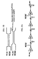
- FIGS. 1A and 1B are an exemplary oscillator biased by a bias generator and a corresponding timing diagram, respectively;
- FIGS. 2A and 2B are an exemplary pulse generator circuit that takes the power down signal as its input and generates a filter bypass pulse signal and a corresponding timing diagram, respectively;
- FIGS. 3A and 3B are an exemplary pulse generator circuit that includes a PMOS transistor that operates as a switch and a corresponding timing diagram, respectively;
- FIG. 4A is an exemplary negative pulse-on-edge circuit, according to one embodiment of the present invention and FIG. 4B depicts a corresponding timing diagram;
- FIGS. 5A and 5B are an exemplary timing delay circuit and a corresponding timing diagram, respectively;
- FIGS. 6A and 6B are an exemplary timing delay circuit and a corresponding timing diagram, respectively;
- FIG. 7A is an exemplary circuit where a positive control signal needs to be generated on rising and falling edge of a control signal and FIG. 7B is a corresponding timing diagram;
- FIG. 8A is an exemplary positive pulse-on-edge circuit that generates an up pulse on each transition of power down signal and FIG. 8B depicts a corresponding timing diagram.
- the present invention is a circuit that takes a single phase clock or control signal as its input and generates a negative pulse on each positive and negative edge of the input signal. In one embodiment, the circuit generates a positive pulse on each edge.
- the circuit according to the invention may be used to generate a pulse that controls a shorting switch to quickly discharge and charge a capacitor, for example, the capacitor of a bias filter.
- the invention allows the bias circuit to start up and shut down quickly, while allowing the filter to remain intact during normal operation.
- the pulse-on-edge circuit may be triggered by a power-down/power-up signal.
- the pulse-on-edge circuit is likewise suitable for various other electronic circuit applications. Accordingly, the described exemplary embodiment of the pulse-on-edge circuit in a bias filter is by way of example only and not by way of limitation.
- FIG. 1A shows an exemplary amplifier being biased by a bias generator.
- the bias generator is controlled by a power down signal A that turns the bias generator off to save power in the power down mode.
- An RC filter is used to limit the noise on the bias voltage to provide a cleaner signal C for the amplifier.
- the noise filter when used on the bias line, in general, it affects the amount of time it takes for the circuit to power up and power down, that is, for the bias voltage to reach its full value at the power up mode and reach its low value at the power down.
- the filter needs to have a low corner frequency. The lower the corner frequency of the filter, the longer it takes to power up and power down the bias voltage. Nevertheless, it is often desirable for the bias voltage to settle quickly to its final state.
- FIG. 1B illustrates an exemplary timing diagram for the circuit of FIG. 1A .
- Node B then quickly transitions from Voff to a desired bias voltage Vbias.
- transition from Voff to Vbias at C occurs slowly as it takes a while to discharge/charge capacitor C through R.
- FIG. 2A shows a pulse generator circuit that takes the power down signal as its input and generates a filter bypass pulse signal, according to one embodiment of the present invention.
- FIG. 2B illustrates an exemplary timing diagram for the circuit of FIG. 2A .
- Node B then quickly transitions from Voff to desired bias voltage Vbias.
- FIG. 3A shows an exemplary pulse generator circuit that includes a PMOS transistor M 3 that operates as a switch. Additionally, the oscillator is shown as a differential oscillator formed by cross-connected NMOS transistors M 1 and M 2 .
- FIG. 3B illustrates an exemplary timing diagram for the circuit of FIG. 3A . As shown in the timing diagram of FIG. 3B , the filter bypass signal D is generated on rising and falling edges of Power down signal A, that is, a down pulse on each transition of A. This ensures the amplifier will power up and power down quickly. In this exemplary case, a PMOS transistor that requires a low voltage to turn on is used as the bypass switch.
- FIG. 4A is an exemplary negative pulse-on-edge circuit, according to one embodiment of the present invention and FIG. 4B depicts a corresponding timing diagram.
- the PMOS transistors M 5 and M 6 are driven by PD_slow and NPD_slow (complement of PD_slow) signals, respectively to pull the node Vpulse having a capacitor Cpar coupled thereto.
- Signals PD_fast, NPD_fast, PD_slow, and NPD_slow drive NMOS transistors M 4 , M 1 , M 3 , and M 2 , respectively.
- PD_slow signal driving the gate of M 5 may be generated from NPD_slow using an inventor.
- the inverter is formed by PMOS transistor M 7 and NMOS transistor M 8 , along with a current source Idc.
- signals NPD_fast, PD_slow, and NPD_slow are generated from PD_fast (power up) signal by a couple of inventors and one or more delay elements, for example RC delays, as shown in FIG. 5A .
- FIG. 5B illustrates a corresponding timing diagram of the inventor-delay of FIG. 5A .
- FIG. 6A shows one exemplary implementation of the RC delay elements, according to one embodiment of the present invention and FIG. 6B depicts a corresponding timing diagram.
- NMOS and PMOS transistors Mr 1 and Mr 2 with narrow width and long channel are used for resistance.
- NMOS and PMOS transistors Mc 1 and Mc 2 with wide width and long channel length are used for Capacitance.
- NPD_slow is low turning the PMOS transistor M 8 off and preventing ldc from passing through M 7 , M 5 which are also off.
- M 3 , M 4 are on, but M 1 , M 2 are off.
- M 6 is also on, pulling Vpulse to VDD.
- region 2 where PD_slow is high, M 3 is turned on, M 1 also turns on overcoming M 6 and pulling Vpulse to GND, because M 1 and M 3 are larger than M 6 .
- M 4 turns off, because PD_fast is low.
- NPD_slow turns M 2 on, but M 4 is already off because PD_fast is low. M 3 and M 6 are also turned off, while M 8 turns on, allowing current to reflect through M 5 . Vpulse node becomes a high impedance node and M 5 is forced into linear region, pulling Vpulse to VDD once again, as shown in the timing diagram.
- M 2 is already on because NPD_slow is high, M 4 also turns on, while M 1 turns off. As a result, Vpulse is pulled down, as shown in the timing diagram of FIG. 4B .
- FIG. 7A illustrates a circuit where a positive control signal, such as the filter bypass signal, needs to be generated on rising and falling edge of a control signal, such as the power down signal, according to one embodiment of the invention.
- a positive control signal such as the filter bypass signal
- a control signal such as the power down signal
- FIG. 7B depicts a corresponding timing diagram for the circuit of FIG. 7A .
- FIG. 8A depicts an exemplary positive pulse-on-edge circuit that generates an up pulse on each transition of the power down (PD) signal.
- FIG. 8B shows a corresponding timing diagram for the circuit of FIG. 8A . The operation of this circuit is similar to the negative pulse-on-edge circuit of FIG. 6A .
- PD_slow is high and thus prevents Idc from passing through transistors M 8 , M 7 , M 5 which are turned off.
- M 3 , M 4 are on, but M 1 , M 2 are off.
- M 6 is on, pulling Vpulse to VDD.
- M 3 is already turned on by a low NPD_slow, M 1 also turns on overcoming M 6 and pulling Vpulse to VDD, because M 1 , M 3 are larger than M 6 .
- M 4 is also turned off by a high NPD_fast.
- M 2 is turned on by a low PD_slow, and M 4 is already off, because NPD_fast is already high.
- M 3 , M 6 turn off and M 8 turns on, allowing current to reflect through M 5 . Accordingly, Vpulse node becomes a high impedance node, M 5 is forced into linear region, pulling Vpulse to GND once again.
- M 2 is already on, M 4 turns on, M 1 turns off, and Vpulse is pulled up to VDD, as shown in the timing diagram.
Abstract
Description
Claims (8)
Priority Applications (1)
| Application Number | Priority Date | Filing Date | Title |
|---|---|---|---|
| US11/563,758 US7342428B2 (en) | 2005-01-06 | 2006-11-28 | Pulse-on-edge circuit |
Applications Claiming Priority (3)
| Application Number | Priority Date | Filing Date | Title |
|---|---|---|---|
| US64223105P | 2005-01-06 | 2005-01-06 | |
| US11/095,238 US7170326B2 (en) | 2005-01-06 | 2005-03-30 | Pulse-on-edge circuit |
| US11/563,758 US7342428B2 (en) | 2005-01-06 | 2006-11-28 | Pulse-on-edge circuit |
Related Parent Applications (1)
| Application Number | Title | Priority Date | Filing Date |
|---|---|---|---|
| US11/095,238 Continuation US7170326B2 (en) | 2005-01-06 | 2005-03-30 | Pulse-on-edge circuit |
Publications (2)
| Publication Number | Publication Date |
|---|---|
| US20070170965A1 US20070170965A1 (en) | 2007-07-26 |
| US7342428B2 true US7342428B2 (en) | 2008-03-11 |
Family
ID=36639680
Family Applications (2)
| Application Number | Title | Priority Date | Filing Date |
|---|---|---|---|
| US11/095,238 Expired - Fee Related US7170326B2 (en) | 2005-01-06 | 2005-03-30 | Pulse-on-edge circuit |
| US11/563,758 Expired - Fee Related US7342428B2 (en) | 2005-01-06 | 2006-11-28 | Pulse-on-edge circuit |
Family Applications Before (1)
| Application Number | Title | Priority Date | Filing Date |
|---|---|---|---|
| US11/095,238 Expired - Fee Related US7170326B2 (en) | 2005-01-06 | 2005-03-30 | Pulse-on-edge circuit |
Country Status (1)
| Country | Link |
|---|---|
| US (2) | US7170326B2 (en) |
Families Citing this family (4)
| Publication number | Priority date | Publication date | Assignee | Title |
|---|---|---|---|---|
| US7915933B2 (en) * | 2006-11-30 | 2011-03-29 | Mosaid Technologies Incorporated | Circuit for clamping current in a charge pump |
| TWI499215B (en) * | 2012-10-17 | 2015-09-01 | Mstar Semiconductor Inc | Charging/discharging circuit and pll utilizing the charging/discharging circuit |
| CN105161798B (en) * | 2015-07-01 | 2017-12-26 | 东南大学 | The SCF and preparation method of silicon substrate low-leakage current cantilever beam grid |
| CN108123708B (en) * | 2016-11-29 | 2021-06-08 | 中芯国际集成电路制造(上海)有限公司 | Pull-up circuit for IO circuit |
Citations (4)
| Publication number | Priority date | Publication date | Assignee | Title |
|---|---|---|---|---|
| US5270580A (en) * | 1991-07-29 | 1993-12-14 | Fujitsu Limited | Pulse generator circuit for producing simultaneous complementary output pulses |
| US5519344A (en) * | 1994-06-30 | 1996-05-21 | Proebsting; Robert J. | Fast propagation technique in CMOS integrated circuits |
| US6060931A (en) | 1998-05-06 | 2000-05-09 | Stahl; George J. | Repetitive pulse generator with wide pulse duration, amplitude, frequency and duty cycle characteristics |
| US6320437B1 (en) | 1998-10-30 | 2001-11-20 | Mosaid Technologies, Inc. | Duty cycle regulator |
-
2005
- 2005-03-30 US US11/095,238 patent/US7170326B2/en not_active Expired - Fee Related
-
2006
- 2006-11-28 US US11/563,758 patent/US7342428B2/en not_active Expired - Fee Related
Patent Citations (4)
| Publication number | Priority date | Publication date | Assignee | Title |
|---|---|---|---|---|
| US5270580A (en) * | 1991-07-29 | 1993-12-14 | Fujitsu Limited | Pulse generator circuit for producing simultaneous complementary output pulses |
| US5519344A (en) * | 1994-06-30 | 1996-05-21 | Proebsting; Robert J. | Fast propagation technique in CMOS integrated circuits |
| US6060931A (en) | 1998-05-06 | 2000-05-09 | Stahl; George J. | Repetitive pulse generator with wide pulse duration, amplitude, frequency and duty cycle characteristics |
| US6320437B1 (en) | 1998-10-30 | 2001-11-20 | Mosaid Technologies, Inc. | Duty cycle regulator |
Also Published As
| Publication number | Publication date |
|---|---|
| US7170326B2 (en) | 2007-01-30 |
| US20060145742A1 (en) | 2006-07-06 |
| US20070170965A1 (en) | 2007-07-26 |
Similar Documents
| Publication | Publication Date | Title |
|---|---|---|
| US6466078B1 (en) | Reduced static phase error CMOS PLL charge pump | |
| US5896043A (en) | Level shift circuit | |
| US7471105B2 (en) | Level shifter and level shifting method for higher speed and lower power | |
| US4739193A (en) | Drive circuit with limited signal transition rate for RFI reduction | |
| US6154078A (en) | Semiconductor buffer circuit with a transition delay circuit | |
| US20240039519A1 (en) | Deglitcher with integrated non-overlap function | |
| US7342428B2 (en) | Pulse-on-edge circuit | |
| KR20040018139A (en) | Control circuit for dc/dc converter | |
| US5598111A (en) | Delay circuit for digital signal processing | |
| US7142024B2 (en) | Power on reset circuit | |
| US7514985B2 (en) | Fast turn on and off speed in PLL cascoded charge pump | |
| US5952851A (en) | Boosted voltage driver | |
| US20140266361A1 (en) | Duty cycle correction circuit | |
| EP1352472B1 (en) | Circuit for receiving and driving a clock-signal | |
| US20060033554A1 (en) | Charge pump circuit | |
| JP2006295362A (en) | Applied voltage control circuit for voltage controlled oscillator circuit | |
| US8736311B2 (en) | Semiconductor integrated circuit | |
| KR100416378B1 (en) | Phase splitter circuit | |
| EP0468210B1 (en) | Circuit for driving a floating circuit in response to a digital signal | |
| US6628151B1 (en) | Self-regulating high voltage ramp up circuit | |
| KR100349356B1 (en) | Power on reset circuit | |
| JPH08102643A (en) | Variable delay circuit, ring oscillation circuit using the delay circuit and pll circuit using the oscillation circuit | |
| JPH0427729B2 (en) | ||
| US7492141B2 (en) | Resonant inverter exhibiting depressed duty variation | |
| KR100316982B1 (en) | Semiconductor memory device having push-pull type output circuit formed by two n-channel mos transistors |
Legal Events
| Date | Code | Title | Description |
|---|---|---|---|
| FPAY | Fee payment |
Year of fee payment: 4 |
|
| REMI | Maintenance fee reminder mailed | ||
| AS | Assignment |
Owner name: BANK OF AMERICA, N.A., AS COLLATERAL AGENT, NORTH CAROLINA Free format text: PATENT SECURITY AGREEMENT;ASSIGNOR:BROADCOM CORPORATION;REEL/FRAME:037806/0001 Effective date: 20160201 Owner name: BANK OF AMERICA, N.A., AS COLLATERAL AGENT, NORTH Free format text: PATENT SECURITY AGREEMENT;ASSIGNOR:BROADCOM CORPORATION;REEL/FRAME:037806/0001 Effective date: 20160201 |
|
| LAPS | Lapse for failure to pay maintenance fees | ||
| STCH | Information on status: patent discontinuation |
Free format text: PATENT EXPIRED DUE TO NONPAYMENT OF MAINTENANCE FEES UNDER 37 CFR 1.362 |
|
| FP | Lapsed due to failure to pay maintenance fee |
Effective date: 20160311 |
|
| AS | Assignment |
Owner name: AVAGO TECHNOLOGIES GENERAL IP (SINGAPORE) PTE. LTD., SINGAPORE Free format text: ASSIGNMENT OF ASSIGNORS INTEREST;ASSIGNOR:BROADCOM CORPORATION;REEL/FRAME:041706/0001 Effective date: 20170120 Owner name: AVAGO TECHNOLOGIES GENERAL IP (SINGAPORE) PTE. LTD Free format text: ASSIGNMENT OF ASSIGNORS INTEREST;ASSIGNOR:BROADCOM CORPORATION;REEL/FRAME:041706/0001 Effective date: 20170120 |
|
| AS | Assignment |
Owner name: BROADCOM CORPORATION, CALIFORNIA Free format text: TERMINATION AND RELEASE OF SECURITY INTEREST IN PATENTS;ASSIGNOR:BANK OF AMERICA, N.A., AS COLLATERAL AGENT;REEL/FRAME:041712/0001 Effective date: 20170119 |
|
| AS | Assignment |
Owner name: AVAGO TECHNOLOGIES INTERNATIONAL SALES PTE. LIMITE Free format text: MERGER;ASSIGNOR:AVAGO TECHNOLOGIES GENERAL IP (SINGAPORE) PTE. LTD.;REEL/FRAME:047195/0658 Effective date: 20180509 |
|
| AS | Assignment |
Owner name: AVAGO TECHNOLOGIES INTERNATIONAL SALES PTE. LIMITE Free format text: CORRECTIVE ASSIGNMENT TO CORRECT THE EFFECTIVE DATE OF MERGER PREVIOUSLY RECORDED ON REEL 047195 FRAME 0658. ASSIGNOR(S) HEREBY CONFIRMS THE THE EFFECTIVE DATE IS 09/05/2018;ASSIGNOR:AVAGO TECHNOLOGIES GENERAL IP (SINGAPORE) PTE. LTD.;REEL/FRAME:047357/0302 Effective date: 20180905 |
|
| AS | Assignment |
Owner name: AVAGO TECHNOLOGIES INTERNATIONAL SALES PTE. LIMITE Free format text: CORRECTIVE ASSIGNMENT TO CORRECT THE ERROR IN RECORDING THE MERGER PREVIOUSLY RECORDED AT REEL: 047357 FRAME: 0302. ASSIGNOR(S) HEREBY CONFIRMS THE ASSIGNMENT;ASSIGNOR:AVAGO TECHNOLOGIES GENERAL IP (SINGAPORE) PTE. LTD.;REEL/FRAME:048674/0834 Effective date: 20180905 |