US7428777B2 - Method of making a heatsink device - Google Patents
Method of making a heatsink device Download PDFInfo
- Publication number
- US7428777B2 US7428777B2 US11/168,616 US16861605A US7428777B2 US 7428777 B2 US7428777 B2 US 7428777B2 US 16861605 A US16861605 A US 16861605A US 7428777 B2 US7428777 B2 US 7428777B2
- Authority
- US
- United States
- Prior art keywords
- heatsink
- powder
- features
- forming
- coupling
- Prior art date
- Legal status (The legal status is an assumption and is not a legal conclusion. Google has not performed a legal analysis and makes no representation as to the accuracy of the status listed.)
- Expired - Fee Related, expires
Links
Images


Classifications
-
- H—ELECTRICITY
- H01—ELECTRIC ELEMENTS
- H01L—SEMICONDUCTOR DEVICES NOT COVERED BY CLASS H10
- H01L23/00—Details of semiconductor or other solid state devices
- H01L23/34—Arrangements for cooling, heating, ventilating or temperature compensation ; Temperature sensing arrangements
- H01L23/36—Selection of materials, or shaping, to facilitate cooling or heating, e.g. heatsinks
- H01L23/367—Cooling facilitated by shape of device
- H01L23/3672—Foil-like cooling fins or heat sinks
-
- F—MECHANICAL ENGINEERING; LIGHTING; HEATING; WEAPONS; BLASTING
- F28—HEAT EXCHANGE IN GENERAL
- F28F—DETAILS OF HEAT-EXCHANGE AND HEAT-TRANSFER APPARATUS, OF GENERAL APPLICATION
- F28F3/00—Plate-like or laminated elements; Assemblies of plate-like or laminated elements
- F28F3/02—Elements or assemblies thereof with means for increasing heat-transfer area, e.g. with fins, with recesses, with corrugations
-
- H—ELECTRICITY
- H01—ELECTRIC ELEMENTS
- H01L—SEMICONDUCTOR DEVICES NOT COVERED BY CLASS H10
- H01L21/00—Processes or apparatus adapted for the manufacture or treatment of semiconductor or solid state devices or of parts thereof
- H01L21/02—Manufacture or treatment of semiconductor devices or of parts thereof
- H01L21/04—Manufacture or treatment of semiconductor devices or of parts thereof the devices having at least one potential-jump barrier or surface barrier, e.g. PN junction, depletion layer or carrier concentration layer
- H01L21/48—Manufacture or treatment of parts, e.g. containers, prior to assembly of the devices, using processes not provided for in a single one of the subgroups H01L21/06 - H01L21/326
- H01L21/4814—Conductive parts
- H01L21/4871—Bases, plates or heatsinks
-
- H—ELECTRICITY
- H01—ELECTRIC ELEMENTS
- H01L—SEMICONDUCTOR DEVICES NOT COVERED BY CLASS H10
- H01L23/00—Details of semiconductor or other solid state devices
- H01L23/34—Arrangements for cooling, heating, ventilating or temperature compensation ; Temperature sensing arrangements
- H01L23/46—Arrangements for cooling, heating, ventilating or temperature compensation ; Temperature sensing arrangements involving the transfer of heat by flowing fluids
- H01L23/467—Arrangements for cooling, heating, ventilating or temperature compensation ; Temperature sensing arrangements involving the transfer of heat by flowing fluids by flowing gases, e.g. air
-
- F—MECHANICAL ENGINEERING; LIGHTING; HEATING; WEAPONS; BLASTING
- F28—HEAT EXCHANGE IN GENERAL
- F28F—DETAILS OF HEAT-EXCHANGE AND HEAT-TRANSFER APPARATUS, OF GENERAL APPLICATION
- F28F2215/00—Fins
- F28F2215/10—Secondary fins, e.g. projections or recesses on main fins
-
- H—ELECTRICITY
- H01—ELECTRIC ELEMENTS
- H01L—SEMICONDUCTOR DEVICES NOT COVERED BY CLASS H10
- H01L2224/00—Indexing scheme for arrangements for connecting or disconnecting semiconductor or solid-state bodies and methods related thereto as covered by H01L24/00
- H01L2224/01—Means for bonding being attached to, or being formed on, the surface to be connected, e.g. chip-to-package, die-attach, "first-level" interconnects; Manufacturing methods related thereto
- H01L2224/10—Bump connectors; Manufacturing methods related thereto
- H01L2224/15—Structure, shape, material or disposition of the bump connectors after the connecting process
- H01L2224/16—Structure, shape, material or disposition of the bump connectors after the connecting process of an individual bump connector
- H01L2224/161—Disposition
- H01L2224/16151—Disposition the bump connector connecting between a semiconductor or solid-state body and an item not being a semiconductor or solid-state body, e.g. chip-to-substrate, chip-to-passive
- H01L2224/16221—Disposition the bump connector connecting between a semiconductor or solid-state body and an item not being a semiconductor or solid-state body, e.g. chip-to-substrate, chip-to-passive the body and the item being stacked
- H01L2224/16225—Disposition the bump connector connecting between a semiconductor or solid-state body and an item not being a semiconductor or solid-state body, e.g. chip-to-substrate, chip-to-passive the body and the item being stacked the item being non-metallic, e.g. insulating substrate with or without metallisation
-
- H—ELECTRICITY
- H01—ELECTRIC ELEMENTS
- H01L—SEMICONDUCTOR DEVICES NOT COVERED BY CLASS H10
- H01L2224/00—Indexing scheme for arrangements for connecting or disconnecting semiconductor or solid-state bodies and methods related thereto as covered by H01L24/00
- H01L2224/01—Means for bonding being attached to, or being formed on, the surface to be connected, e.g. chip-to-package, die-attach, "first-level" interconnects; Manufacturing methods related thereto
- H01L2224/26—Layer connectors, e.g. plate connectors, solder or adhesive layers; Manufacturing methods related thereto
- H01L2224/31—Structure, shape, material or disposition of the layer connectors after the connecting process
- H01L2224/32—Structure, shape, material or disposition of the layer connectors after the connecting process of an individual layer connector
- H01L2224/321—Disposition
- H01L2224/32151—Disposition the layer connector connecting between a semiconductor or solid-state body and an item not being a semiconductor or solid-state body, e.g. chip-to-substrate, chip-to-passive
- H01L2224/32221—Disposition the layer connector connecting between a semiconductor or solid-state body and an item not being a semiconductor or solid-state body, e.g. chip-to-substrate, chip-to-passive the body and the item being stacked
- H01L2224/32225—Disposition the layer connector connecting between a semiconductor or solid-state body and an item not being a semiconductor or solid-state body, e.g. chip-to-substrate, chip-to-passive the body and the item being stacked the item being non-metallic, e.g. insulating substrate with or without metallisation
-
- H—ELECTRICITY
- H01—ELECTRIC ELEMENTS
- H01L—SEMICONDUCTOR DEVICES NOT COVERED BY CLASS H10
- H01L2224/00—Indexing scheme for arrangements for connecting or disconnecting semiconductor or solid-state bodies and methods related thereto as covered by H01L24/00
- H01L2224/73—Means for bonding being of different types provided for in two or more of groups H01L2224/10, H01L2224/18, H01L2224/26, H01L2224/34, H01L2224/42, H01L2224/50, H01L2224/63, H01L2224/71
- H01L2224/732—Location after the connecting process
- H01L2224/73201—Location after the connecting process on the same surface
- H01L2224/73203—Bump and layer connectors
- H01L2224/73204—Bump and layer connectors the bump connector being embedded into the layer connector
-
- H—ELECTRICITY
- H01—ELECTRIC ELEMENTS
- H01L—SEMICONDUCTOR DEVICES NOT COVERED BY CLASS H10
- H01L2224/00—Indexing scheme for arrangements for connecting or disconnecting semiconductor or solid-state bodies and methods related thereto as covered by H01L24/00
- H01L2224/73—Means for bonding being of different types provided for in two or more of groups H01L2224/10, H01L2224/18, H01L2224/26, H01L2224/34, H01L2224/42, H01L2224/50, H01L2224/63, H01L2224/71
- H01L2224/732—Location after the connecting process
- H01L2224/73251—Location after the connecting process on different surfaces
- H01L2224/73253—Bump and layer connectors
-
- H—ELECTRICITY
- H01—ELECTRIC ELEMENTS
- H01L—SEMICONDUCTOR DEVICES NOT COVERED BY CLASS H10
- H01L2924/00—Indexing scheme for arrangements or methods for connecting or disconnecting semiconductor or solid-state bodies as covered by H01L24/00
- H01L2924/0001—Technical content checked by a classifier
- H01L2924/00014—Technical content checked by a classifier the subject-matter covered by the group, the symbol of which is combined with the symbol of this group, being disclosed without further technical details
-
- H—ELECTRICITY
- H01—ELECTRIC ELEMENTS
- H01L—SEMICONDUCTOR DEVICES NOT COVERED BY CLASS H10
- H01L2924/00—Indexing scheme for arrangements or methods for connecting or disconnecting semiconductor or solid-state bodies as covered by H01L24/00
- H01L2924/15—Details of package parts other than the semiconductor or other solid state devices to be connected
- H01L2924/151—Die mounting substrate
- H01L2924/153—Connection portion
- H01L2924/1531—Connection portion the connection portion being formed only on the surface of the substrate opposite to the die mounting surface
- H01L2924/15311—Connection portion the connection portion being formed only on the surface of the substrate opposite to the die mounting surface being a ball array, e.g. BGA
-
- Y—GENERAL TAGGING OF NEW TECHNOLOGICAL DEVELOPMENTS; GENERAL TAGGING OF CROSS-SECTIONAL TECHNOLOGIES SPANNING OVER SEVERAL SECTIONS OF THE IPC; TECHNICAL SUBJECTS COVERED BY FORMER USPC CROSS-REFERENCE ART COLLECTIONS [XRACs] AND DIGESTS
- Y02—TECHNOLOGIES OR APPLICATIONS FOR MITIGATION OR ADAPTATION AGAINST CLIMATE CHANGE
- Y02P—CLIMATE CHANGE MITIGATION TECHNOLOGIES IN THE PRODUCTION OR PROCESSING OF GOODS
- Y02P80/00—Climate change mitigation technologies for sector-wide applications
- Y02P80/30—Reducing waste in manufacturing processes; Calculations of released waste quantities
-
- Y—GENERAL TAGGING OF NEW TECHNOLOGICAL DEVELOPMENTS; GENERAL TAGGING OF CROSS-SECTIONAL TECHNOLOGIES SPANNING OVER SEVERAL SECTIONS OF THE IPC; TECHNICAL SUBJECTS COVERED BY FORMER USPC CROSS-REFERENCE ART COLLECTIONS [XRACs] AND DIGESTS
- Y10—TECHNICAL SUBJECTS COVERED BY FORMER USPC
- Y10T—TECHNICAL SUBJECTS COVERED BY FORMER US CLASSIFICATION
- Y10T29/00—Metal working
- Y10T29/49—Method of mechanical manufacture
- Y10T29/49002—Electrical device making
- Y10T29/49117—Conductor or circuit manufacturing
- Y10T29/49124—On flat or curved insulated base, e.g., printed circuit, etc.
- Y10T29/4913—Assembling to base an electrical component, e.g., capacitor, etc.
- Y10T29/49144—Assembling to base an electrical component, e.g., capacitor, etc. by metal fusion
Definitions
- the present invention relates generally to the field of heat transfer and, in particular, the present invention relates to thermal management of electronic devices.
- heatsinks are used to transfer heat generated by electronic devices or groups of devices, such as transistors, as are commonly included on integrated circuit (IC) chips such as processor chips.
- IC integrated circuit
- FIG. 1 illustrates an information handling device according to one embodiment of the invention.
- FIG. 2A illustrates a side view of a processor assembly according to one embodiment of the invention.
- FIG. 2B illustrates an isometric view of a processor assembly according to one embodiment of the invention.
- FIG. 3 illustrates a top view of a heatsink according to one embodiment of the invention.
- FIG. 4 illustrates a flow chart of a method of forming a heatsink according to one embodiment of the invention.
- FIG. 5A illustrates an isometric view of a portion of a heatsink according to one embodiment of the invention.
- FIG. 5B illustrates a top view of a portion of a heatsink according to one embodiment of the invention.
- FIG. 5C illustrates a top view of a portion of a heatsink according to one embodiment of the invention.
- FIG. 6 illustrates an isometric view of a heatsink according to one embodiment of the invention.
- active side as used in this description is defined as the conventional horizontal, large plane or surface of a chip or die where electrical devices have typically been fabricated, regardless of the orientation of the chip or die.
- back side as used in this description is defined as a conventional horizontal, large plane or surface of a chip or die that generally does not contain active devices on its surface.
- vertical refers to a direction perpendicular to the horizontal as defined above. Prepositions, such as “on”, “higher”, “lower”, “above” and “below” are defined with respect to the conventional plane or surface being on the active side of the chip or die, regardless of the orientation of the chip or die.
- FIG. 1 is a block diagram of an information handling system 1 incorporating at least one heatsink in accordance with at least one embodiment of the invention.
- Information handling system 1 is merely one example of an electronic system in which the present invention can be used.
- information handling system 1 comprises a data processing system that includes a system bus 2 to couple the various components of the system.
- System bus 2 provides communications links among the various components of the information handling system 1 and can be implemented as a single bus, as a combination of busses, or in any other suitable manner.
- Electronic assembly 4 is coupled to system bus 2 .
- Electronic assembly 4 can include any circuit or combination of circuits.
- electronic assembly 4 includes a processor 6 which can be of any type.
- processor means any type of computational circuit, such as but not limited to a microprocessor, a microcontroller, a complex instruction set computing (CISC) microprocessor, a reduced instruction set computing (RISC) microprocessor, a very long instruction word (VLIW) microprocessor, a graphics processor, a digital signal processor (DSP), or any other type of processor or processing circuit.
- CISC complex instruction set computing
- RISC reduced instruction set computing
- VLIW very long instruction word
- DSP digital signal processor
- circuits that can be included in electronic assembly 4 are a custom circuit, an application-specific integrated circuit (ASIC), or the like, such as, for example, one or more circuits (such as a communications circuit 7 ) for use in wireless devices like cellular telephones, pagers, portable computers, two-way radios, and similar electronic systems.
- ASIC application-specific integrated circuit
- the IC can perform any other type of function.
- Information handling system 1 can also include an external memory 10 , which in turn can include one or more memory elements suitable to the particular application, such as a main memory 12 in the form of random access memory (RAM), one or more hard drives 14 , and/or one or more drives that handle removable media 16 such as floppy diskettes, compact disks (CD), digital video disk (DVD), and the like.
- main memory 12 include dynamic random access memory (DRAM), synchronous dynamic random access memory (SDRAM), double data rate synchronous dynamic random access memory (DDR SDRAM), rambus dynamic random access memory (RDRAM), flash memory, static random access memory (SRAM), etc.
- Information handling system 1 can also include a display device 8 , one or more speakers 9 , and a keyboard and/or controller 20 , which can include a mouse, trackball, game controller, voice-recognition device, or any other device that permits a system user to input information into and receive information from the information handling system 1 .
- a display device 8 can also include a mouse, trackball, game controller, voice-recognition device, or any other device that permits a system user to input information into and receive information from the information handling system 1 .
- a keyboard and/or controller 20 which can include a mouse, trackball, game controller, voice-recognition device, or any other device that permits a system user to input information into and receive information from the information handling system 1 .
- the present invention is found to be effective at transferring heat from IC surfaces, the invention is not limited to heat transfer from IC surfaces.
- the invention can be used in any setting where heat is to be conducted from one surface to another.
- the example of cooling an IC will be used.
- FIG. 2A shows a cross-sectional representation of a chip assembly 200 .
- the chip assembly can be termed a processor assembly.
- Chip assembly 200 includes an IC die 210 mounted in “flip-chip” orientation with its active side facing downward to couple with an upper surface of a substrate 220 , such as a circuit board, through solder balls or bumps 212 .
- Substrate 220 can be a one-layer board or a multi-layer board, and it can include additional contacts 222 on its opposite surface for mating with additional packaging structure (not shown).
- Die 210 generates its heat from internal structure, including wiring traces, that is located near its active side; however, a significant portion of the heat is dissipated through its back side 214 .
- Heat that is concentrated within the die is dissipated to a large surface that is in contact with the die in the form of an integrated heat spreader 230 that is typically formed of metal such as copper or aluminum.
- the integrated heat spreader 230 is formed into a partial enclosure, and serves as a package cover for the die 210 .
- a sealant 234 is further included to isolate and secure the integrated heat spreader 230 to the substrate 220 .
- a thermal interface material 240 is often provided between the die 210 and integrated heat spreader 230 .
- a heatsink 250 optionally having fins 252 is coupled to the integrated heat spreader 230 .
- Heatsink 250 dissipates heat into the ambient environment.
- a second thermal interface material 254 is further utilized to create a thermal pathway between the integrated heat spreader 230 and the heatsink 250 .
- a device such as a fan is connected adjacent to the heatsink 250 to circulate air and more effectively transfer heat away from the die 210 .
- the heatsink 250 shown in FIG. 2A is intended to be a general illustration of a heatsink. In the following detailed description, specific details of heatsinks and assemblies are illustrated for given embodiments of the invention.
- FIG. 2B shows an embodiment of an chip assembly 200 without an additional heatsink 250 attached as described above.
- the integrated heat spreader 230 is shown in an embodiment formed as a package cover. The edges of the integrated heat spreader 230 form an enclosure with the substrate 220 where the die (not shown) is substantially enclosed.
- an opening 232 is included in the integrated heat spreader 230 . In one embodiment, the opening 232 provides a relief for variations in pressure due to thermal changes in the die.
- FIG. 3 shows an embodiment of a heatsink 300 .
- the heatsink 300 includes a base portion 310 with a number of heat transfer features 320 coupled to the base portion 310 .
- the number of heat transfer features 320 includes a number of fins.
- the number of heat transfer features 320 are shaped in an arcuate shape as shown in FIG. 3 .
- the base portion 310 includes a center 312 and the number of heat transfer features 320 are arranged in a substantially radial pattern about the center 312 .
- the number of heat transfer features 320 are arranged with radial symmetry about the center 312 , but the heat transfer features 320 themselves are not necessarily oriented radially.
- a number of sub-features 330 are also shown. In one embodiment, a number of sub-features 330 are attached to at least one feature 320 . In one embodiment, a number of sub-features 330 are attached to each heat transfer features 320 . In one embodiment the number of sub-features 330 includes a number of sub-fins.
- fin is a broad term that encompasses several geometries that are generally long and substantially flat. Fin geometries are not necessarily straight. For example, fins include arcuate shapes as shown in FIG. 3 .
- features of the heatsink 300 are formed using a sintered powder manufacturing process.
- the sintered powder manufacturing process includes powder metallurgy.
- heat transfer features 320 and sub-features 330 are formed using a powder metallurgy process.
- the base portion 310 is formed using a powder metallurgy process.
- the base portion 310 , the heat transfer features 320 , and the sub-features 330 are formed integrally using a powder metallurgy process.
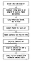
- FIG. 4 shows a flow diagram of a method according to one embodiment used to form at least a portion of a heatsink using a powder metallurgy process.
- a geometry for the heatsink is designed.
- a computer aided design (CAD) program such as AutoCAD, ProE, etc. is used to design the geometry of the heatsink.
- CAD computer aided design
- a form is constructed in a negative image of the heatsink.
- the form is constructed using data from the CAD geometry of the heatsink.
- a powder base material is placed within the form to substantially fill regions of the form that will become the eventual heatsink or heatsink component.
- the powder base material is further compacted into the form under pressure from a piston, or other compression device to promote filling of detailed features in the form. Selected embodiments do not include compaction of the powder base material.
- powdered base material include, but are not limited to aluminum, copper, magnesium, etc.
- a composite powder base material is used. Examples of composite powdered base material include, but are not limited to aluminum and aluminum oxide; copper and tungsten, etc.
- a form is used that is open on opposing longitudinal ends.
- the powder base material is compacted using a piston like device.
- the compacted unit is held together temporarily from the pressing operation by mechanisms such as cold welds at the particle contact points or by the presence of a binder material additive in the powder base material.
- a lubricant is used in the powder base material to further promote compaction.
- the compacted unit is then removed from the form prior to sintering.
- the lubricant further aids in removal of the unit of pressed powder particles from the form.
- the piston like device is further used to push the compacted unit out of the form through one of the open ends of the form.
- the unit of pressed powder particles is sintered to transform the powder into a solid unit.
- temperatures below a melting temperature of the powder base material are used to sinter the powder base material.
- powder particles diffuse together at contact points to form a solid connection between the individual powder particles. Processing conditions such as time, temperature, and sintering atmosphere are adjusted for sintering depending on the specific powder base materials being sintered.
- One advantage of manufacture using powder metallurgy includes the fine surface finish of the unit directly after the sintering process.
- Other processes such as casting require additional manufacturing steps after the unit is formed.
- cast parts require a machining operation after casting to remove unwanted protrusions left from the casting process.
- Another advantage of manufacture using powder metallurgy includes the ability to form detailed features.
- Features with intricate detail such as sub-features 330 illustrated in FIG. 3 cannot be formed using other less detail capable processes such as casting or extrusion.
- problems such as removal of the cast part from a casting mold prohibit formation of intricate features.
- powder metallurgy a component of a heatsink is compacted in a form, then pressed out of the form prior to sintering. Details such as sub-fins 330 are not broken off during removal of the unit of pressed powder particles from the form, and the intricate features are solidified during the sintering operation.
- Another advantage of manufacture using powder metallurgy includes the reduction of waste of raw materials. Because little or no machining is needed after formation of the heatsink or heatsink component, less material is wasted in the form of machining scraps.
- a composition of a composite powdered base material is only possible using powder metallurgy techniques.
- Some heat sink materials may be incompatible with each other using manufacturing techniques such as casting. Elements of a composite material for a casting process may not melt together due to differing melting temperatures, or unwanted chemical phases may develop in a casting process.
- powder metallurgy allows a wide range of composite materials that are not practical for formation using techniques such as casting.
- high melting temperature single component powders can also be formed using powder metallurgy techniques.
- casting formation of components using metals such as refractory metals is not practical due to the extremely high temperatures necessary to melt refractory metals.
- refractory metals include tungsten, titanium, vanadium, etc.
- powder metallurgy techniques can be uniquely used to form heatsink structures from selected metals such as refractory metals.
- high extrusion force materials can be formed using powder metallurgy techniques. Because powder metallurgy does not require extrusion forces to form solid structures, powder metallurgy techniques can be uniquely used to form heatsink structures from high hardness, or brittle materials that are difficult or impossible to extrude.
- a sintered heatsink or heatsink component is further coupled to a device such as a chip assembly. Further, in one embodiment, a device such as a chip assembly including a sintered heatsink or heatsink component is further coupled into a system such as an information handling system.
- FIG. 5A shows one configuration of a portion of a heatsink 500 .
- the portion of the heatsink 500 includes a fin 520 and a number of sub-fins 530 .
- One advantage of heatsink designs that use a number of sub-fins 530 includes increased surface area of the heatsink. As described above, several configurations of sub-fins 530 or sub-features cannot be formed using manufacturing methods such as casting or extrusion.
- FIG. 5A illustrates one embodiment of geometry of the number of sub-fins 530 .
- the following equations illustrate how the use of sub-fins 530 leads to a large increase in surface area of a resulting heatsink.
- FIG. 5A illustrates one embodiment of geometry of the number of sub-fins 530 .
- the following equations illustrate how the use of sub-fins 530 leads to a large increase in surface area of a resulting heatsink.
- sub-fins 530 include an arcuate profile 531 to enhance surface area in a given volume, other geometries of sub-fins or sub-features are also within the scope of the invention.
- FIG. 5B shows an example of a portion of a heatsink 502 .
- the portion of the heatsink 502 includes a fin 522 and a number of sub-fins 532 .
- the sub-fins 522 include a number of rectangular sub-fins.
- FIG. 5C likewise illustrates an example of a portion of a heatsink 504 .
- the portion of the heatsink 504 includes a fin 524 and a number of sub-fins 534 .
- the sub-fins 522 include a number of triangular sub-fins.
- FIG. 6 shows an embodiment of a heatsink 600 .
- the heatsink 600 includes a base portion 610 with a number of heat transfer features 620 coupled to the base portion 310 .
- the number of heat transfer features 620 includes a number of fins.
- the number of heat transfer features 620 are shaped in an arcuate shape as shown in FIG. 6 .
- the base portion 610 includes a center 312 and the number of heat transfer features 620 are arranged in a substantially radial pattern about the center 612 .
- the number of heat transfer features 620 are arranged with radial symmetry about the center 612 , but the heat transfer features 620 themselves are not necessarily oriented radially.
- all edges of the heat transfer features 620 are parallel to a longitudinal axis of the heatsink 300 .
- heat transfer features 620 are formed using a powder metallurgy process as described in embodiments above.
- the base portion 610 is formed using a powder metallurgy process as described in embodiments above.
- at least part of the base portion 610 and the heat transfer features 620 are formed integrally using a powder metallurgy process as described in embodiments above.
- the number of heat transfer features 620 located about the base portion 610 can be increased due to the use of powder metallurgy techniques as described in embodiments above. Powder metallurgy provides capabilities to increase the number of heat transfer features 620 similar to capabilities needed to form numbers of sub-features as described above.
- the base portion 610 includes an insert 614 within a part of the base portion 610 .
- the insert 614 includes a material of a different composition from the remaining base portion 610 or number of heat transfer features 620 .
- the insert 614 includes a material with a higher thermal conductivity than the remaining base portion 610 or number of heat transfer features 620 .
- the insert 614 includes copper. Factors for selection of the material and geometry for the insert 614 include thermal performance, weight, and cost for the thermal solution.
- One advantage of a composite heatsink 600 using an insert 614 includes the ability to achieve high thermal conductivity in the insert 614 using materials such as copper, while maintaining a low weight and low cost using other materials such as aluminum for the number of heat transfer features 620 .
- Methods of forming heatsinks as described above include advantages such as the ability to produce intricate detailed features that other manufacturing methods are not capable of. Other advantages include a reduction in process time and cost due to the absence of a need to machine components after initial fabrication.
- Embodiments of devices formed by the methods described above include features such as sub-fins and other detailed features that cannot be formed using other manufacturing processes. Further embodiments of devices formed by the methods described above include materials that cannot be formed using other manufacturing processes.
Abstract
A method and device for thermal conduction is provided. Methods of forming heatsinks are provided that include advantages such as the ability to produce intricate detailed features that other manufacturing methods are not capable of. Other advantages provided include a reduction in process time and cost due to the absence of a need to machine components after initial fabrication. Embodiments of heatsinks that are formed using methods provided include features such as sub-fins and other detailed features that cannot be formed using other manufacturing processes. Further embodiments of heatsinks that are formed using methods provided include materials that cannot be formed using other manufacturing processes.
Description
This application is a Divisional of U.S. application Ser. No. 10/610,348 filed Jun. 30, 2003 now U.S Pat. No. 6,937,473, which is incorporated herein by reference.
The present invention relates generally to the field of heat transfer and, in particular, the present invention relates to thermal management of electronic devices.
In one aspect of heat transfer technology, heatsinks are used to transfer heat generated by electronic devices or groups of devices, such as transistors, as are commonly included on integrated circuit (IC) chips such as processor chips.
In the field of electronic systems there is an incessant competitive pressure among manufacturers to drive the performance of their equipment up while driving down production costs. This is particularly true regarding forming electronic devices such as transistors in IC's, where each new generation of IC must provide increased performance, particularly in terms of an increased number of devices and higher clock frequencies, while generally being smaller or more compact in size. As the density and clock frequency of IC's increase, they accordingly generate a greater amount of heat. However, the performance and reliability of IC's are known to diminish as the temperature to which they are subjected increases, so it becomes increasingly important to adequately dissipate heat from IC environments.
With the advent of high performance IC's and their associated packages, electronic devices have required more innovative thermal management to dissipate heat. Increasing speed and power in processors, for example, generally carry with it a “cost” of increased heat in the microelectronic die that must be dissipated. What is needed is a device and method to more effectively cool microelectronic dies containing IC's such as processors. What is also needed is a device and method that is less expensive and easier to manufacture.
In the following detailed description of the invention reference is made to the accompanying drawings which form a part hereof, and in which are shown, by way of illustration, specific embodiments in which the invention may be practiced. In the drawings, like numerals describe substantially similar components throughout the several views. These embodiments are described in sufficient detail to enable those skilled in the art to practice the invention. Other embodiments may be utilized, and structural, logical, and electrical changes may be made, without departing from the scope of the present invention. The following detailed description is, therefore, not to be taken in a limiting sense, and the scope of the invention should be determined with reference to the appended claims, along with the full scope of equivalents to which such claims are entitled.
The term “active side” as used in this description is defined as the conventional horizontal, large plane or surface of a chip or die where electrical devices have typically been fabricated, regardless of the orientation of the chip or die. The term “back side” as used in this description is defined as a conventional horizontal, large plane or surface of a chip or die that generally does not contain active devices on its surface. The term “vertical” refers to a direction perpendicular to the horizontal as defined above. Prepositions, such as “on”, “higher”, “lower”, “above” and “below” are defined with respect to the conventional plane or surface being on the active side of the chip or die, regardless of the orientation of the chip or die.
An example of an information handling system using processor chips and thermal management devices is included to show an example of a higher level device application for the present invention. FIG. 1 is a block diagram of an information handling system 1 incorporating at least one heatsink in accordance with at least one embodiment of the invention. Information handling system 1 is merely one example of an electronic system in which the present invention can be used. In this example, information handling system 1 comprises a data processing system that includes a system bus 2 to couple the various components of the system. System bus 2 provides communications links among the various components of the information handling system 1 and can be implemented as a single bus, as a combination of busses, or in any other suitable manner.
Electronic assembly 4 is coupled to system bus 2. Electronic assembly 4 can include any circuit or combination of circuits. In one embodiment, electronic assembly 4 includes a processor 6 which can be of any type. As used herein, “processor” means any type of computational circuit, such as but not limited to a microprocessor, a microcontroller, a complex instruction set computing (CISC) microprocessor, a reduced instruction set computing (RISC) microprocessor, a very long instruction word (VLIW) microprocessor, a graphics processor, a digital signal processor (DSP), or any other type of processor or processing circuit.
Other types of circuits that can be included in electronic assembly 4 are a custom circuit, an application-specific integrated circuit (ASIC), or the like, such as, for example, one or more circuits (such as a communications circuit 7) for use in wireless devices like cellular telephones, pagers, portable computers, two-way radios, and similar electronic systems. The IC can perform any other type of function.
Information handling system 1 can also include an external memory 10, which in turn can include one or more memory elements suitable to the particular application, such as a main memory 12 in the form of random access memory (RAM), one or more hard drives 14, and/or one or more drives that handle removable media 16 such as floppy diskettes, compact disks (CD), digital video disk (DVD), and the like. Examples of main memory 12 include dynamic random access memory (DRAM), synchronous dynamic random access memory (SDRAM), double data rate synchronous dynamic random access memory (DDR SDRAM), rambus dynamic random access memory (RDRAM), flash memory, static random access memory (SRAM), etc.
Information handling system 1 can also include a display device 8, one or more speakers 9, and a keyboard and/or controller 20, which can include a mouse, trackball, game controller, voice-recognition device, or any other device that permits a system user to input information into and receive information from the information handling system 1.
Although the present invention is found to be effective at transferring heat from IC surfaces, the invention is not limited to heat transfer from IC surfaces. The invention can be used in any setting where heat is to be conducted from one surface to another. For ease of explanation, the example of cooling an IC will be used.
Die 210 generates its heat from internal structure, including wiring traces, that is located near its active side; however, a significant portion of the heat is dissipated through its back side 214. Heat that is concentrated within the die is dissipated to a large surface that is in contact with the die in the form of an integrated heat spreader 230 that is typically formed of metal such as copper or aluminum. In one embodiment, the integrated heat spreader 230 is formed into a partial enclosure, and serves as a package cover for the die 210. In one embodiment, a sealant 234 is further included to isolate and secure the integrated heat spreader 230 to the substrate 220. To improve the thermal conductivity between the die 210 and the integrated heat spreader 230, a thermal interface material 240 is often provided between the die 210 and integrated heat spreader 230.
In one embodiment, to further dissipate heat from the integrated heat spreader 230, a heatsink 250 optionally having fins 252 is coupled to the integrated heat spreader 230. Heatsink 250 dissipates heat into the ambient environment. In one embodiment a second thermal interface material 254 is further utilized to create a thermal pathway between the integrated heat spreader 230 and the heatsink 250. In one embodiment, a device such as a fan is connected adjacent to the heatsink 250 to circulate air and more effectively transfer heat away from the die 210.
The heatsink 250 shown in FIG. 2A is intended to be a general illustration of a heatsink. In the following detailed description, specific details of heatsinks and assemblies are illustrated for given embodiments of the invention.
A number of sub-features 330 are also shown. In one embodiment, a number of sub-features 330 are attached to at least one feature 320. In one embodiment, a number of sub-features 330 are attached to each heat transfer features 320. In one embodiment the number of sub-features 330 includes a number of sub-fins. One of ordinary skill in the art, having the benefit of the present disclosure will recognize that the term “fin” is a broad term that encompasses several geometries that are generally long and substantially flat. Fin geometries are not necessarily straight. For example, fins include arcuate shapes as shown in FIG. 3 . One of ordinary skill in the art, having the benefit of the present disclosure will recognize that other geometries of heat conducting features apart from fins can also be used in embodiments of heatsinks as shown. In one embodiment, all edges of the heat transfer features 320 and the number of sub-features 330 are parallel to a longitudinal axis of the heatsink 300.
In one embodiment, features of the heatsink 300 are formed using a sintered powder manufacturing process. In one embodiment, the sintered powder manufacturing process includes powder metallurgy. In one embodiment, heat transfer features 320 and sub-features 330 are formed using a powder metallurgy process. In one embodiment, the base portion 310 is formed using a powder metallurgy process. In one embodiment, the base portion 310, the heat transfer features 320, and the sub-features 330 are formed integrally using a powder metallurgy process.
In one embodiment a powder base material is placed within the form to substantially fill regions of the form that will become the eventual heatsink or heatsink component. In one embodiment, the powder base material is further compacted into the form under pressure from a piston, or other compression device to promote filling of detailed features in the form. Selected embodiments do not include compaction of the powder base material. Examples of powdered base material include, but are not limited to aluminum, copper, magnesium, etc. In one embodiment, a composite powder base material is used. Examples of composite powdered base material include, but are not limited to aluminum and aluminum oxide; copper and tungsten, etc. Although metal base materials are described, other base materials such as ceramic base materials are possible.
In one embodiment using compaction of the powder base material, a form is used that is open on opposing longitudinal ends. In one embodiment, the powder base material is compacted using a piston like device. In one operation, the compacted unit is held together temporarily from the pressing operation by mechanisms such as cold welds at the particle contact points or by the presence of a binder material additive in the powder base material. In one embodiment a lubricant is used in the powder base material to further promote compaction. In one embodiment, the compacted unit is then removed from the form prior to sintering. In one embodiment, the lubricant further aids in removal of the unit of pressed powder particles from the form. In one embodiment, the piston like device is further used to push the compacted unit out of the form through one of the open ends of the form.
In one operation the unit of pressed powder particles is sintered to transform the powder into a solid unit. In one embodiment temperatures below a melting temperature of the powder base material are used to sinter the powder base material. During one sintering operation, at a temperature below a melting temperature, powder particles diffuse together at contact points to form a solid connection between the individual powder particles. Processing conditions such as time, temperature, and sintering atmosphere are adjusted for sintering depending on the specific powder base materials being sintered.
One advantage of manufacture using powder metallurgy includes the fine surface finish of the unit directly after the sintering process. Other processes such as casting require additional manufacturing steps after the unit is formed. For example, cast parts require a machining operation after casting to remove unwanted protrusions left from the casting process.
Another advantage of manufacture using powder metallurgy includes the ability to form detailed features. Features with intricate detail such as sub-features 330 illustrated in FIG. 3 cannot be formed using other less detail capable processes such as casting or extrusion. In casting, problems such as removal of the cast part from a casting mold prohibit formation of intricate features. In contrast, in one embodiment using powder metallurgy, a component of a heatsink is compacted in a form, then pressed out of the form prior to sintering. Details such as sub-fins 330 are not broken off during removal of the unit of pressed powder particles from the form, and the intricate features are solidified during the sintering operation. Likewise, in an extrusion process, intricate features such as sub-fins 330 are broken or torn due to the forces needed to extrude the material through a die. No mechanical forces are used during a sintering operation of powder metallurgy.
Another advantage of manufacture using powder metallurgy includes the reduction of waste of raw materials. Because little or no machining is needed after formation of the heatsink or heatsink component, less material is wasted in the form of machining scraps.
In one embodiment a composition of a composite powdered base material is only possible using powder metallurgy techniques. Some heat sink materials may be incompatible with each other using manufacturing techniques such as casting. Elements of a composite material for a casting process may not melt together due to differing melting temperatures, or unwanted chemical phases may develop in a casting process. In contrast, powder metallurgy allows a wide range of composite materials that are not practical for formation using techniques such as casting.
Further, high melting temperature single component powders can also be formed using powder metallurgy techniques. For example, casting formation of components using metals such as refractory metals is not practical due to the extremely high temperatures necessary to melt refractory metals. Examples of refractory metals include tungsten, titanium, vanadium, etc. Because powder metallurgy does not require melting to form solid structures, powder metallurgy techniques can be uniquely used to form heatsink structures from selected metals such as refractory metals.
Likewise, high extrusion force materials can be formed using powder metallurgy techniques. Because powder metallurgy does not require extrusion forces to form solid structures, powder metallurgy techniques can be uniquely used to form heatsink structures from high hardness, or brittle materials that are difficult or impossible to extrude.
As shown in the flowchart of FIG. 4 , in selected higher level applications, a sintered heatsink or heatsink component is further coupled to a device such as a chip assembly. Further, in one embodiment, a device such as a chip assembly including a sintered heatsink or heatsink component is further coupled into a system such as an information handling system.
-
- a is the length between the pitch in the fin
- b is the height of the sub-fin
- c is the width of the fin.
- The surface area per pitch without the sub-fin, A=c×a
- The surface area per pitch with the sub-fin, A′=c×a+2(b×c)
- The percentage of the increase in surface area,
-
- If b=0.5a, then, the percentage of the increase in surface area will be 100%.
Given that heat dissipation, Hd α Areasurface the increase in the surface area increases heat dissipation efficiency.
- If b=0.5a, then, the percentage of the increase in surface area will be 100%.
Although specific examples of dimensions a, b, and c are given above, the values are intended only as an example. Likewise, although the sub-fins 530 include an arcuate profile 531 to enhance surface area in a given volume, other geometries of sub-fins or sub-features are also within the scope of the invention.
In one embodiment, heat transfer features 620 are formed using a powder metallurgy process as described in embodiments above. In one embodiment, the base portion 610 is formed using a powder metallurgy process as described in embodiments above. In one embodiment, at least part of the base portion 610 and the heat transfer features 620 are formed integrally using a powder metallurgy process as described in embodiments above.
In one embodiment the number of heat transfer features 620 located about the base portion 610 can be increased due to the use of powder metallurgy techniques as described in embodiments above. Powder metallurgy provides capabilities to increase the number of heat transfer features 620 similar to capabilities needed to form numbers of sub-features as described above.
In one embodiment, the base portion 610 includes an insert 614 within a part of the base portion 610. In one embodiment, the insert 614 includes a material of a different composition from the remaining base portion 610 or number of heat transfer features 620. In one embodiment, the insert 614 includes a material with a higher thermal conductivity than the remaining base portion 610 or number of heat transfer features 620. In one embodiment, the insert 614 includes copper. Factors for selection of the material and geometry for the insert 614 include thermal performance, weight, and cost for the thermal solution. One advantage of a composite heatsink 600 using an insert 614 includes the ability to achieve high thermal conductivity in the insert 614 using materials such as copper, while maintaining a low weight and low cost using other materials such as aluminum for the number of heat transfer features 620.
Methods of forming heatsinks as described above include advantages such as the ability to produce intricate detailed features that other manufacturing methods are not capable of. Other advantages include a reduction in process time and cost due to the absence of a need to machine components after initial fabrication. Embodiments of devices formed by the methods described above include features such as sub-fins and other detailed features that cannot be formed using other manufacturing processes. Further embodiments of devices formed by the methods described above include materials that cannot be formed using other manufacturing processes.
Although specific embodiments have been illustrated and described herein, it will be appreciated by those of ordinary skill in the art that any arrangement which is calculated to achieve the same purpose may be substituted for the specific embodiment shown. This application is intended to cover any adaptations or variations of embodiments described above. It is to be understood that the above description is intended to be illustrative, and not restrictive. Combinations of the above embodiments, and other embodiments will be apparent to those of skill in the art upon reviewing the above description. The scope of the invention includes any other applications in which the above structures and fabrication methods are used. The scope of the invention should be determined with reference to the appended claims, along with the full scope of equivalents to which such claims are entitled.
Claims (8)
1. A method of forming an information handling system, comprising:
forming a processor assembly including:
attaching a processor chip to a substrate;
coupling a package cover to the processor chip;
forming a heatsink, including:
constructing a heatsink form with a number of heatsink forming features and two opposing open ends;
placing an amount of powder into the heatsink form;
heating the amount of powder to a sintering temperature;
sintering the powder to form a bond between powder particles in the powder;
removing a heatsink unit from the heatsink form by pressing the heatsink unit out of the heatsink form through one of the open ends of the heatsink form, the heatsink unit being formed from the sintered powder;
coupling the heatsink unit to a surface of the package cover; and
connecting a bus between the processor chip and a dynamic random access memory.
2. The method of claim 1 , wherein constructing the heatsink form includes constructing a heatsink form with features for forming a number of radial fins.
3. The method of claim 1 , wherein constructing the heatsink form includes constructing a heatsink form with features for forming a number of radial fins and a number of sub-fins attached to at least one of the number of radial fins.
4. The method of claim 1 , wherein placing the amount of powder into the heatsink form includes placing an amount of metal powder into the heatsink form.
5. The method of claim 1 , wherein connecting a bus between the processor chip and a dynamic random access memory includes connecting a bus between the processor chip and a double data rate dynamic random access memory.
6. A method of forming an information handling system, comprising:
forming a processor assembly including:
attaching a processor chip to a substrate;
coupling a package cover to the processor chip;
coupling a heatsink unit to a surface of the package cover, wherein at least a portion of the heatsink is formed using powder sintering techniques using a heatsink form with a number of heatsink forming features and two opposing open ends and removing the heatsink from the heatsink form by pressing the heatsink out of the heatsink form through one of the open ends of the heatsink form; and
connecting a bus between the processor chip and a dynamic random access memory.
7. The method of claim 6 , wherein coupling the heatsink unit includes coupling a heatsink unit to a surface of the package cover, wherein at least a portion of the heatsink is formed using metal powder sintering techniques.
8. The method of claim 6 , wherein coupling the heatsink unit includes coupling a heatsink unit to the surface of the package cover, wherein the heatsink unit includes a number of radial fins and a number of sub-fins attached to at least one of the number of radial fins.
Priority Applications (1)
| Application Number | Priority Date | Filing Date | Title |
|---|---|---|---|
| US11/168,616 US7428777B2 (en) | 2003-06-30 | 2005-06-28 | Method of making a heatsink device |
Applications Claiming Priority (2)
| Application Number | Priority Date | Filing Date | Title |
|---|---|---|---|
| US10/610,348 US6937473B2 (en) | 2003-06-30 | 2003-06-30 | Heatsink device and method |
| US11/168,616 US7428777B2 (en) | 2003-06-30 | 2005-06-28 | Method of making a heatsink device |
Related Parent Applications (1)
| Application Number | Title | Priority Date | Filing Date |
|---|---|---|---|
| US10/610,348 Division US6937473B2 (en) | 2003-06-30 | 2003-06-30 | Heatsink device and method |
Publications (2)
| Publication Number | Publication Date |
|---|---|
| US20050255646A1 US20050255646A1 (en) | 2005-11-17 |
| US7428777B2 true US7428777B2 (en) | 2008-09-30 |
Family
ID=33541126
Family Applications (2)
| Application Number | Title | Priority Date | Filing Date |
|---|---|---|---|
| US10/610,348 Expired - Fee Related US6937473B2 (en) | 2003-06-30 | 2003-06-30 | Heatsink device and method |
| US11/168,616 Expired - Fee Related US7428777B2 (en) | 2003-06-30 | 2005-06-28 | Method of making a heatsink device |
Family Applications Before (1)
| Application Number | Title | Priority Date | Filing Date |
|---|---|---|---|
| US10/610,348 Expired - Fee Related US6937473B2 (en) | 2003-06-30 | 2003-06-30 | Heatsink device and method |
Country Status (1)
| Country | Link |
|---|---|
| US (2) | US6937473B2 (en) |
Cited By (1)
| Publication number | Priority date | Publication date | Assignee | Title |
|---|---|---|---|---|
| US20090321923A1 (en) * | 2008-06-30 | 2009-12-31 | Rajasekaran Swaminathan | Magnetic particle-based composite materials for semiconductor packages |
Families Citing this family (29)
| Publication number | Priority date | Publication date | Assignee | Title |
|---|---|---|---|---|
| US6671172B2 (en) * | 2001-09-10 | 2003-12-30 | Intel Corporation | Electronic assemblies with high capacity curved fin heat sinks |
| US6937473B2 (en) * | 2003-06-30 | 2005-08-30 | Intel Corporation | Heatsink device and method |
| US8020608B2 (en) * | 2004-08-31 | 2011-09-20 | Hewlett-Packard Development Company, L.P. | Heat sink fin with stator blade |
| US7286352B2 (en) * | 2005-04-15 | 2007-10-23 | Hewlett-Packard Development Company, L.P. | Thermally expanding base of heatsink to receive fins |
| US20070034173A1 (en) * | 2005-08-09 | 2007-02-15 | Lee Chang C | Upright heat dispensing fins of cylinder body |
| US7269013B2 (en) * | 2006-01-09 | 2007-09-11 | Fu Zhun Prexision Industry (Shan Zhen) Co., Ltd. | Heat dissipation device having phase-changeable medium therein |
| US7535099B2 (en) * | 2006-09-26 | 2009-05-19 | Intel Corporation | Sintered metallic thermal interface materials for microelectronic cooling assemblies |
| US20090014856A1 (en) * | 2007-07-10 | 2009-01-15 | International Business Machine Corporation | Microbump seal |
| US7845393B2 (en) * | 2007-11-06 | 2010-12-07 | Jiing Tung Tec. Metal Co., Ltd. | Thermal module |
| EP2202475B1 (en) * | 2008-12-23 | 2012-05-02 | Ching-Sung Kuo | Wing-spanning thermal-dissipating device |
| US7984250B2 (en) * | 2008-12-31 | 2011-07-19 | Intel Corporation | Dynamic updating of thresholds in accordance with operating conditons |
| US10103089B2 (en) * | 2010-03-26 | 2018-10-16 | Hamilton Sundstrand Corporation | Heat transfer device with fins defining air flow channels |
| US10041745B2 (en) | 2010-05-04 | 2018-08-07 | Fractal Heatsink Technologies LLC | Fractal heat transfer device |
| US10852069B2 (en) | 2010-05-04 | 2020-12-01 | Fractal Heatsink Technologies, LLC | System and method for maintaining efficiency of a fractal heat sink |
| US9228785B2 (en) | 2010-05-04 | 2016-01-05 | Alexander Poltorak | Fractal heat transfer device |
| US8295046B2 (en) * | 2010-07-19 | 2012-10-23 | Hamilton Sundstrand Corporation | Non-circular radial heat sink |
| CN103260923B (en) | 2010-12-07 | 2016-12-21 | 艾里逊变速箱公司 | Energy storage system for hybrid-power electric vehicle |
| JP5893838B2 (en) * | 2011-03-18 | 2016-03-23 | 新光電気工業株式会社 | Heat dissipation component, semiconductor package having the same, and method for manufacturing heat dissipation component |
| US11129299B2 (en) * | 2011-03-31 | 2021-09-21 | Tejas Network Limited | Heat sink |
| US20220120517A1 (en) * | 2011-05-12 | 2022-04-21 | Fractal Heatsink Technologies LLC | Fractal heat transfer device |
| TW201321710A (en) * | 2011-11-29 | 2013-06-01 | Foxsemicon Integrated Tech Inc | Heat sink and LED lamp using the same |
| JP2014103184A (en) * | 2012-11-19 | 2014-06-05 | Nippon Densan Corp | Heat sink and heat sink fan |
| CN103117275B (en) * | 2013-01-31 | 2015-08-19 | 华为技术有限公司 | A kind of chip-packaging structure and chip packaging method |
| JP5997207B2 (en) * | 2014-06-17 | 2016-09-28 | ファナック株式会社 | Control panel cooling device |
| WO2018013668A1 (en) | 2016-07-12 | 2018-01-18 | Alexander Poltorak | System and method for maintaining efficiency of a heat sink |
| US11031312B2 (en) | 2017-07-17 | 2021-06-08 | Fractal Heatsink Technologies, LLC | Multi-fractal heatsink system and method |
| US11488887B1 (en) * | 2020-03-05 | 2022-11-01 | Xilinx, Inc. | Thermal enablement of dies with impurity gettering |
| WO2022067589A1 (en) * | 2020-09-29 | 2022-04-07 | 华为技术有限公司 | Chip package and electronic device |
| FI130775B1 (en) * | 2020-11-13 | 2024-03-12 | Thermal Channel Tech Oy | Heat sink as well as apparatus and method of producing the same |
Citations (18)
| Publication number | Priority date | Publication date | Assignee | Title |
|---|---|---|---|---|
| US5413751A (en) * | 1993-04-14 | 1995-05-09 | Frank J. Polese | Method for making heat-dissipating elements for micro-electronic devices |
| US5673174A (en) | 1995-03-23 | 1997-09-30 | Nexar Technologies, Inc. | System permitting the external replacement of the CPU and/or DRAM SIMMs microchip boards |
| US5972737A (en) * | 1993-04-14 | 1999-10-26 | Frank J. Polese | Heat-dissipating package for microcircuit devices and process for manufacture |
| US6015008A (en) | 1997-07-14 | 2000-01-18 | Mitsubishi Electric Home Appliance Co., Ltd. | Heat radiating plate |
| US6183874B1 (en) * | 1996-06-14 | 2001-02-06 | Sumitomo Electric Industries, Ltd. | Substrate material for mounting a semiconductor device, substrate for mounting a semiconductor device, semiconductor device, and method of producing the same |
| US6196298B1 (en) | 1997-03-22 | 2001-03-06 | Imi Marston Limited | Heat sink |
| US6250127B1 (en) * | 1999-10-11 | 2001-06-26 | Polese Company, Inc. | Heat-dissipating aluminum silicon carbide composite manufacturing method |
| USD450306S1 (en) | 2001-05-18 | 2001-11-13 | Enlight Corporation | Heat sink |
| US6418020B1 (en) | 2001-03-30 | 2002-07-09 | Advanced Thermal Technologies | Heat dissipation device with ribbed fin plates |
| US6462413B1 (en) * | 1999-07-22 | 2002-10-08 | Polese Company, Inc. | LDMOS transistor heatsink package assembly and manufacturing method |
| USD464939S1 (en) | 2001-12-26 | 2002-10-29 | Thermal Integration Technology Inc. | Heat sink |
| US6505680B1 (en) | 2001-07-27 | 2003-01-14 | Hewlett-Packard Company | High performance cooling device |
| US20030024693A1 (en) | 2001-07-31 | 2003-02-06 | Petty Eric Hayes | Counter flow two pass active heat sink with heat spreader |
| US6569524B2 (en) * | 2000-06-23 | 2003-05-27 | Sumitomo Electric Industries, Ltd. | High thermal conductivity composite material, and method for producing the same |
| US6671172B2 (en) | 2001-09-10 | 2003-12-30 | Intel Corporation | Electronic assemblies with high capacity curved fin heat sinks |
| US6714415B1 (en) | 2003-03-13 | 2004-03-30 | Intel Corporation | Split fin heat sink |
| US20040264134A1 (en) | 2003-06-30 | 2004-12-30 | Cheng Kai Yong | Heatsink device and method |
| US7047639B1 (en) * | 2005-04-25 | 2006-05-23 | Actron Technology Corporation | Method for manufacturing a heat-dissipating structure of a rectifier |
-
2003
- 2003-06-30 US US10/610,348 patent/US6937473B2/en not_active Expired - Fee Related
-
2005
- 2005-06-28 US US11/168,616 patent/US7428777B2/en not_active Expired - Fee Related
Patent Citations (19)
| Publication number | Priority date | Publication date | Assignee | Title |
|---|---|---|---|---|
| US5972737A (en) * | 1993-04-14 | 1999-10-26 | Frank J. Polese | Heat-dissipating package for microcircuit devices and process for manufacture |
| US5413751A (en) * | 1993-04-14 | 1995-05-09 | Frank J. Polese | Method for making heat-dissipating elements for micro-electronic devices |
| US5673174A (en) | 1995-03-23 | 1997-09-30 | Nexar Technologies, Inc. | System permitting the external replacement of the CPU and/or DRAM SIMMs microchip boards |
| US6534190B1 (en) * | 1996-06-14 | 2003-03-18 | Sumitomo Electric Industries, Ltd. | Substrate material for mounting a semiconductor device, substrate for mounting a semiconductor device, semiconductor device, and method of producing the same |
| US6183874B1 (en) * | 1996-06-14 | 2001-02-06 | Sumitomo Electric Industries, Ltd. | Substrate material for mounting a semiconductor device, substrate for mounting a semiconductor device, semiconductor device, and method of producing the same |
| US6196298B1 (en) | 1997-03-22 | 2001-03-06 | Imi Marston Limited | Heat sink |
| US6015008A (en) | 1997-07-14 | 2000-01-18 | Mitsubishi Electric Home Appliance Co., Ltd. | Heat radiating plate |
| US6462413B1 (en) * | 1999-07-22 | 2002-10-08 | Polese Company, Inc. | LDMOS transistor heatsink package assembly and manufacturing method |
| US6250127B1 (en) * | 1999-10-11 | 2001-06-26 | Polese Company, Inc. | Heat-dissipating aluminum silicon carbide composite manufacturing method |
| US6569524B2 (en) * | 2000-06-23 | 2003-05-27 | Sumitomo Electric Industries, Ltd. | High thermal conductivity composite material, and method for producing the same |
| US6418020B1 (en) | 2001-03-30 | 2002-07-09 | Advanced Thermal Technologies | Heat dissipation device with ribbed fin plates |
| USD450306S1 (en) | 2001-05-18 | 2001-11-13 | Enlight Corporation | Heat sink |
| US6505680B1 (en) | 2001-07-27 | 2003-01-14 | Hewlett-Packard Company | High performance cooling device |
| US20030024693A1 (en) | 2001-07-31 | 2003-02-06 | Petty Eric Hayes | Counter flow two pass active heat sink with heat spreader |
| US6671172B2 (en) | 2001-09-10 | 2003-12-30 | Intel Corporation | Electronic assemblies with high capacity curved fin heat sinks |
| USD464939S1 (en) | 2001-12-26 | 2002-10-29 | Thermal Integration Technology Inc. | Heat sink |
| US6714415B1 (en) | 2003-03-13 | 2004-03-30 | Intel Corporation | Split fin heat sink |
| US20040264134A1 (en) | 2003-06-30 | 2004-12-30 | Cheng Kai Yong | Heatsink device and method |
| US7047639B1 (en) * | 2005-04-25 | 2006-05-23 | Actron Technology Corporation | Method for manufacturing a heat-dissipating structure of a rectifier |
Non-Patent Citations (1)
| Title |
|---|
| Research Disclosure "Thermal Cap with Direct Heat Sink" (Published Sep. 1986) Research Disclosure Database No. 269021, Research Disclosure Journal No. 26921. |
Cited By (4)
| Publication number | Priority date | Publication date | Assignee | Title |
|---|---|---|---|---|
| US20090321923A1 (en) * | 2008-06-30 | 2009-12-31 | Rajasekaran Swaminathan | Magnetic particle-based composite materials for semiconductor packages |
| US7906376B2 (en) * | 2008-06-30 | 2011-03-15 | Intel Corporation | Magnetic particle-based composite materials for semiconductor packages |
| US20110127663A1 (en) * | 2008-06-30 | 2011-06-02 | Rajasekaran Swaminathan | Magnetic particle-based composite materials for semiconductor packages |
| US8222730B2 (en) | 2008-06-30 | 2012-07-17 | Intel Corporation | Magnetic particle-based composite materials for semiconductor packages |
Also Published As
| Publication number | Publication date |
|---|---|
| US20050255646A1 (en) | 2005-11-17 |
| US20040264134A1 (en) | 2004-12-30 |
| US6937473B2 (en) | 2005-08-30 |
Similar Documents
| Publication | Publication Date | Title |
|---|---|---|
| US7428777B2 (en) | Method of making a heatsink device | |
| US7464462B2 (en) | Method of forming anisotropic heat spreading apparatus for semiconductor devices | |
| US7169650B2 (en) | Semi-solid metal injection methods for electronic assembly thermal interface | |
| US7327027B2 (en) | Thermal interface structure with integrated liquid cooling and methods | |
| US7886813B2 (en) | Thermal interface material with carbon nanotubes and particles | |
| US6987671B2 (en) | Composite thermal interface devices and methods for integrated circuit heat transfer | |
| US7704798B2 (en) | Electronic assemblies with hot spot cooling and methods relating thereto | |
| US6756669B2 (en) | Heat spreader with down set leg attachment feature | |
| KR20070120917A (en) | Thermal improvement for hotspots on dies in integrated circuit packages | |
| US7347354B2 (en) | Metallic solder thermal interface material layer and application of the same | |
| US10748833B2 (en) | Fan-out semiconductor package | |
| US20070124934A1 (en) | Water Block And Manufacturing Method Thereof | |
| US6479895B1 (en) | High performance air cooled heat sinks used in high density packaging applications | |
| US7082031B2 (en) | Heatsink device and method | |
| JP2004518536A (en) | Heat dissipation device by injection molding | |
| US20030051867A1 (en) | High heat flux heat sink and method of creating same | |
| US20210134698A1 (en) | Thermal interface structures for integrated circuit packages | |
| US20050269675A1 (en) | Internal package heat dissipator | |
| US20210143082A1 (en) | Plastic crystal thermal interface materials | |
| JP2002110874A (en) | Heat sink and its producing method | |
| JP2006210611A (en) | Heat sink equipped with radiation fin, and manufacturing method thereof | |
| US11721607B2 (en) | Integrated circuit assemblies having metal foam structures | |
| TWI384936B (en) | Manufacturing methods of heat dissipation apparatus and two-phase heat exchange device | |
| US20210398871A1 (en) | Integrated circuit heat spreader including sealant interface material | |
| WO2023250035A1 (en) | Metallic thermal interface materials and associated devices, systems, and methods |
Legal Events
| Date | Code | Title | Description |
|---|---|---|---|
| FEPP | Fee payment procedure |
Free format text: PAYOR NUMBER ASSIGNED (ORIGINAL EVENT CODE: ASPN); ENTITY STATUS OF PATENT OWNER: LARGE ENTITY |
|
| FPAY | Fee payment |
Year of fee payment: 4 |
|
| REMI | Maintenance fee reminder mailed | ||
| LAPS | Lapse for failure to pay maintenance fees | ||
| STCH | Information on status: patent discontinuation |
Free format text: PATENT EXPIRED DUE TO NONPAYMENT OF MAINTENANCE FEES UNDER 37 CFR 1.362 |
|
| FP | Lapsed due to failure to pay maintenance fee |
Effective date: 20160930 |