US7429790B2 - Semiconductor structure and method of manufacture - Google Patents
Semiconductor structure and method of manufacture Download PDFInfo
- Publication number
- US7429790B2 US7429790B2 US11/257,783 US25778305A US7429790B2 US 7429790 B2 US7429790 B2 US 7429790B2 US 25778305 A US25778305 A US 25778305A US 7429790 B2 US7429790 B2 US 7429790B2
- Authority
- US
- United States
- Prior art keywords
- substrate
- semiconductor
- mold lock
- flange
- electrical
- Prior art date
- Legal status (The legal status is an assumption and is not a legal conclusion. Google has not performed a legal analysis and makes no representation as to the accuracy of the status listed.)
- Active, expires
Links
Images


Classifications
-
- H—ELECTRICITY
- H01—ELECTRIC ELEMENTS
- H01L—SEMICONDUCTOR DEVICES NOT COVERED BY CLASS H10
- H01L23/00—Details of semiconductor or other solid state devices
- H01L23/12—Mountings, e.g. non-detachable insulating substrates
- H01L23/13—Mountings, e.g. non-detachable insulating substrates characterised by the shape
-
- H—ELECTRICITY
- H01—ELECTRIC ELEMENTS
- H01L—SEMICONDUCTOR DEVICES NOT COVERED BY CLASS H10
- H01L23/00—Details of semiconductor or other solid state devices
- H01L23/02—Containers; Seals
- H01L23/10—Containers; Seals characterised by the material or arrangement of seals between parts, e.g. between cap and base of the container or between leads and walls of the container
-
- H—ELECTRICITY
- H01—ELECTRIC ELEMENTS
- H01L—SEMICONDUCTOR DEVICES NOT COVERED BY CLASS H10
- H01L24/00—Arrangements for connecting or disconnecting semiconductor or solid-state bodies; Methods or apparatus related thereto
- H01L24/01—Means for bonding being attached to, or being formed on, the surface to be connected, e.g. chip-to-package, die-attach, "first-level" interconnects; Manufacturing methods related thereto
- H01L24/42—Wire connectors; Manufacturing methods related thereto
- H01L24/47—Structure, shape, material or disposition of the wire connectors after the connecting process
- H01L24/49—Structure, shape, material or disposition of the wire connectors after the connecting process of a plurality of wire connectors
-
- H—ELECTRICITY
- H01—ELECTRIC ELEMENTS
- H01L—SEMICONDUCTOR DEVICES NOT COVERED BY CLASS H10
- H01L2224/00—Indexing scheme for arrangements for connecting or disconnecting semiconductor or solid-state bodies and methods related thereto as covered by H01L24/00
- H01L2224/01—Means for bonding being attached to, or being formed on, the surface to be connected, e.g. chip-to-package, die-attach, "first-level" interconnects; Manufacturing methods related thereto
- H01L2224/42—Wire connectors; Manufacturing methods related thereto
- H01L2224/44—Structure, shape, material or disposition of the wire connectors prior to the connecting process
- H01L2224/45—Structure, shape, material or disposition of the wire connectors prior to the connecting process of an individual wire connector
- H01L2224/45001—Core members of the connector
- H01L2224/45099—Material
- H01L2224/451—Material with a principal constituent of the material being a metal or a metalloid, e.g. boron (B), silicon (Si), germanium (Ge), arsenic (As), antimony (Sb), tellurium (Te) and polonium (Po), and alloys thereof
- H01L2224/45101—Material with a principal constituent of the material being a metal or a metalloid, e.g. boron (B), silicon (Si), germanium (Ge), arsenic (As), antimony (Sb), tellurium (Te) and polonium (Po), and alloys thereof the principal constituent melting at a temperature of less than 400°C
- H01L2224/45111—Tin (Sn) as principal constituent
-
- H—ELECTRICITY
- H01—ELECTRIC ELEMENTS
- H01L—SEMICONDUCTOR DEVICES NOT COVERED BY CLASS H10
- H01L2224/00—Indexing scheme for arrangements for connecting or disconnecting semiconductor or solid-state bodies and methods related thereto as covered by H01L24/00
- H01L2224/01—Means for bonding being attached to, or being formed on, the surface to be connected, e.g. chip-to-package, die-attach, "first-level" interconnects; Manufacturing methods related thereto
- H01L2224/42—Wire connectors; Manufacturing methods related thereto
- H01L2224/44—Structure, shape, material or disposition of the wire connectors prior to the connecting process
- H01L2224/45—Structure, shape, material or disposition of the wire connectors prior to the connecting process of an individual wire connector
- H01L2224/45001—Core members of the connector
- H01L2224/45099—Material
- H01L2224/451—Material with a principal constituent of the material being a metal or a metalloid, e.g. boron (B), silicon (Si), germanium (Ge), arsenic (As), antimony (Sb), tellurium (Te) and polonium (Po), and alloys thereof
- H01L2224/45117—Material with a principal constituent of the material being a metal or a metalloid, e.g. boron (B), silicon (Si), germanium (Ge), arsenic (As), antimony (Sb), tellurium (Te) and polonium (Po), and alloys thereof the principal constituent melting at a temperature of greater than or equal to 400°C and less than 950°C
- H01L2224/45124—Aluminium (Al) as principal constituent
-
- H—ELECTRICITY
- H01—ELECTRIC ELEMENTS
- H01L—SEMICONDUCTOR DEVICES NOT COVERED BY CLASS H10
- H01L2224/00—Indexing scheme for arrangements for connecting or disconnecting semiconductor or solid-state bodies and methods related thereto as covered by H01L24/00
- H01L2224/01—Means for bonding being attached to, or being formed on, the surface to be connected, e.g. chip-to-package, die-attach, "first-level" interconnects; Manufacturing methods related thereto
- H01L2224/42—Wire connectors; Manufacturing methods related thereto
- H01L2224/44—Structure, shape, material or disposition of the wire connectors prior to the connecting process
- H01L2224/45—Structure, shape, material or disposition of the wire connectors prior to the connecting process of an individual wire connector
- H01L2224/45001—Core members of the connector
- H01L2224/45099—Material
- H01L2224/451—Material with a principal constituent of the material being a metal or a metalloid, e.g. boron (B), silicon (Si), germanium (Ge), arsenic (As), antimony (Sb), tellurium (Te) and polonium (Po), and alloys thereof
- H01L2224/45138—Material with a principal constituent of the material being a metal or a metalloid, e.g. boron (B), silicon (Si), germanium (Ge), arsenic (As), antimony (Sb), tellurium (Te) and polonium (Po), and alloys thereof the principal constituent melting at a temperature of greater than or equal to 950°C and less than 1550°C
- H01L2224/45144—Gold (Au) as principal constituent
-
- H—ELECTRICITY
- H01—ELECTRIC ELEMENTS
- H01L—SEMICONDUCTOR DEVICES NOT COVERED BY CLASS H10
- H01L2224/00—Indexing scheme for arrangements for connecting or disconnecting semiconductor or solid-state bodies and methods related thereto as covered by H01L24/00
- H01L2224/01—Means for bonding being attached to, or being formed on, the surface to be connected, e.g. chip-to-package, die-attach, "first-level" interconnects; Manufacturing methods related thereto
- H01L2224/42—Wire connectors; Manufacturing methods related thereto
- H01L2224/44—Structure, shape, material or disposition of the wire connectors prior to the connecting process
- H01L2224/45—Structure, shape, material or disposition of the wire connectors prior to the connecting process of an individual wire connector
- H01L2224/45001—Core members of the connector
- H01L2224/45099—Material
- H01L2224/451—Material with a principal constituent of the material being a metal or a metalloid, e.g. boron (B), silicon (Si), germanium (Ge), arsenic (As), antimony (Sb), tellurium (Te) and polonium (Po), and alloys thereof
- H01L2224/45138—Material with a principal constituent of the material being a metal or a metalloid, e.g. boron (B), silicon (Si), germanium (Ge), arsenic (As), antimony (Sb), tellurium (Te) and polonium (Po), and alloys thereof the principal constituent melting at a temperature of greater than or equal to 950°C and less than 1550°C
- H01L2224/45147—Copper (Cu) as principal constituent
-
- H—ELECTRICITY
- H01—ELECTRIC ELEMENTS
- H01L—SEMICONDUCTOR DEVICES NOT COVERED BY CLASS H10
- H01L2224/00—Indexing scheme for arrangements for connecting or disconnecting semiconductor or solid-state bodies and methods related thereto as covered by H01L24/00
- H01L2224/01—Means for bonding being attached to, or being formed on, the surface to be connected, e.g. chip-to-package, die-attach, "first-level" interconnects; Manufacturing methods related thereto
- H01L2224/42—Wire connectors; Manufacturing methods related thereto
- H01L2224/47—Structure, shape, material or disposition of the wire connectors after the connecting process
- H01L2224/48—Structure, shape, material or disposition of the wire connectors after the connecting process of an individual wire connector
- H01L2224/4805—Shape
- H01L2224/4809—Loop shape
- H01L2224/48091—Arched
-
- H—ELECTRICITY
- H01—ELECTRIC ELEMENTS
- H01L—SEMICONDUCTOR DEVICES NOT COVERED BY CLASS H10
- H01L2224/00—Indexing scheme for arrangements for connecting or disconnecting semiconductor or solid-state bodies and methods related thereto as covered by H01L24/00
- H01L2224/01—Means for bonding being attached to, or being formed on, the surface to be connected, e.g. chip-to-package, die-attach, "first-level" interconnects; Manufacturing methods related thereto
- H01L2224/42—Wire connectors; Manufacturing methods related thereto
- H01L2224/47—Structure, shape, material or disposition of the wire connectors after the connecting process
- H01L2224/48—Structure, shape, material or disposition of the wire connectors after the connecting process of an individual wire connector
- H01L2224/481—Disposition
- H01L2224/48151—Connecting between a semiconductor or solid-state body and an item not being a semiconductor or solid-state body, e.g. chip-to-substrate, chip-to-passive
- H01L2224/48221—Connecting between a semiconductor or solid-state body and an item not being a semiconductor or solid-state body, e.g. chip-to-substrate, chip-to-passive the body and the item being stacked
- H01L2224/48245—Connecting between a semiconductor or solid-state body and an item not being a semiconductor or solid-state body, e.g. chip-to-substrate, chip-to-passive the body and the item being stacked the item being metallic
- H01L2224/48247—Connecting between a semiconductor or solid-state body and an item not being a semiconductor or solid-state body, e.g. chip-to-substrate, chip-to-passive the body and the item being stacked the item being metallic connecting the wire to a bond pad of the item
-
- H—ELECTRICITY
- H01—ELECTRIC ELEMENTS
- H01L—SEMICONDUCTOR DEVICES NOT COVERED BY CLASS H10
- H01L2224/00—Indexing scheme for arrangements for connecting or disconnecting semiconductor or solid-state bodies and methods related thereto as covered by H01L24/00
- H01L2224/01—Means for bonding being attached to, or being formed on, the surface to be connected, e.g. chip-to-package, die-attach, "first-level" interconnects; Manufacturing methods related thereto
- H01L2224/42—Wire connectors; Manufacturing methods related thereto
- H01L2224/47—Structure, shape, material or disposition of the wire connectors after the connecting process
- H01L2224/48—Structure, shape, material or disposition of the wire connectors after the connecting process of an individual wire connector
- H01L2224/484—Connecting portions
- H01L2224/48463—Connecting portions the connecting portion on the bonding area of the semiconductor or solid-state body being a ball bond
- H01L2224/48464—Connecting portions the connecting portion on the bonding area of the semiconductor or solid-state body being a ball bond the other connecting portion not on the bonding area also being a ball bond, i.e. ball-to-ball
-
- H—ELECTRICITY
- H01—ELECTRIC ELEMENTS
- H01L—SEMICONDUCTOR DEVICES NOT COVERED BY CLASS H10
- H01L2224/00—Indexing scheme for arrangements for connecting or disconnecting semiconductor or solid-state bodies and methods related thereto as covered by H01L24/00
- H01L2224/01—Means for bonding being attached to, or being formed on, the surface to be connected, e.g. chip-to-package, die-attach, "first-level" interconnects; Manufacturing methods related thereto
- H01L2224/42—Wire connectors; Manufacturing methods related thereto
- H01L2224/47—Structure, shape, material or disposition of the wire connectors after the connecting process
- H01L2224/49—Structure, shape, material or disposition of the wire connectors after the connecting process of a plurality of wire connectors
-
- H—ELECTRICITY
- H01—ELECTRIC ELEMENTS
- H01L—SEMICONDUCTOR DEVICES NOT COVERED BY CLASS H10
- H01L2224/00—Indexing scheme for arrangements for connecting or disconnecting semiconductor or solid-state bodies and methods related thereto as covered by H01L24/00
- H01L2224/73—Means for bonding being of different types provided for in two or more of groups H01L2224/10, H01L2224/18, H01L2224/26, H01L2224/34, H01L2224/42, H01L2224/50, H01L2224/63, H01L2224/71
- H01L2224/732—Location after the connecting process
- H01L2224/73251—Location after the connecting process on different surfaces
- H01L2224/73265—Layer and wire connectors
-
- H—ELECTRICITY
- H01—ELECTRIC ELEMENTS
- H01L—SEMICONDUCTOR DEVICES NOT COVERED BY CLASS H10
- H01L2224/00—Indexing scheme for arrangements for connecting or disconnecting semiconductor or solid-state bodies and methods related thereto as covered by H01L24/00
- H01L2224/91—Methods for connecting semiconductor or solid state bodies including different methods provided for in two or more of groups H01L2224/80 - H01L2224/90
- H01L2224/92—Specific sequence of method steps
- H01L2224/922—Connecting different surfaces of the semiconductor or solid-state body with connectors of different types
- H01L2224/9222—Sequential connecting processes
- H01L2224/92242—Sequential connecting processes the first connecting process involving a layer connector
- H01L2224/92247—Sequential connecting processes the first connecting process involving a layer connector the second connecting process involving a wire connector
-
- H—ELECTRICITY
- H01—ELECTRIC ELEMENTS
- H01L—SEMICONDUCTOR DEVICES NOT COVERED BY CLASS H10
- H01L24/00—Arrangements for connecting or disconnecting semiconductor or solid-state bodies; Methods or apparatus related thereto
- H01L24/01—Means for bonding being attached to, or being formed on, the surface to be connected, e.g. chip-to-package, die-attach, "first-level" interconnects; Manufacturing methods related thereto
- H01L24/42—Wire connectors; Manufacturing methods related thereto
- H01L24/44—Structure, shape, material or disposition of the wire connectors prior to the connecting process
- H01L24/45—Structure, shape, material or disposition of the wire connectors prior to the connecting process of an individual wire connector
-
- H—ELECTRICITY
- H01—ELECTRIC ELEMENTS
- H01L—SEMICONDUCTOR DEVICES NOT COVERED BY CLASS H10
- H01L24/00—Arrangements for connecting or disconnecting semiconductor or solid-state bodies; Methods or apparatus related thereto
- H01L24/01—Means for bonding being attached to, or being formed on, the surface to be connected, e.g. chip-to-package, die-attach, "first-level" interconnects; Manufacturing methods related thereto
- H01L24/42—Wire connectors; Manufacturing methods related thereto
- H01L24/47—Structure, shape, material or disposition of the wire connectors after the connecting process
- H01L24/48—Structure, shape, material or disposition of the wire connectors after the connecting process of an individual wire connector
-
- H—ELECTRICITY
- H01—ELECTRIC ELEMENTS
- H01L—SEMICONDUCTOR DEVICES NOT COVERED BY CLASS H10
- H01L2924/00—Indexing scheme for arrangements or methods for connecting or disconnecting semiconductor or solid-state bodies as covered by H01L24/00
- H01L2924/01—Chemical elements
- H01L2924/01007—Nitrogen [N]
-
- H—ELECTRICITY
- H01—ELECTRIC ELEMENTS
- H01L—SEMICONDUCTOR DEVICES NOT COVERED BY CLASS H10
- H01L2924/00—Indexing scheme for arrangements or methods for connecting or disconnecting semiconductor or solid-state bodies as covered by H01L24/00
- H01L2924/01—Chemical elements
- H01L2924/01013—Aluminum [Al]
-
- H—ELECTRICITY
- H01—ELECTRIC ELEMENTS
- H01L—SEMICONDUCTOR DEVICES NOT COVERED BY CLASS H10
- H01L2924/00—Indexing scheme for arrangements or methods for connecting or disconnecting semiconductor or solid-state bodies as covered by H01L24/00
- H01L2924/01—Chemical elements
- H01L2924/01014—Silicon [Si]
-
- H—ELECTRICITY
- H01—ELECTRIC ELEMENTS
- H01L—SEMICONDUCTOR DEVICES NOT COVERED BY CLASS H10
- H01L2924/00—Indexing scheme for arrangements or methods for connecting or disconnecting semiconductor or solid-state bodies as covered by H01L24/00
- H01L2924/01—Chemical elements
- H01L2924/01025—Manganese [Mn]
-
- H—ELECTRICITY
- H01—ELECTRIC ELEMENTS
- H01L—SEMICONDUCTOR DEVICES NOT COVERED BY CLASS H10
- H01L2924/00—Indexing scheme for arrangements or methods for connecting or disconnecting semiconductor or solid-state bodies as covered by H01L24/00
- H01L2924/01—Chemical elements
- H01L2924/01027—Cobalt [Co]
-
- H—ELECTRICITY
- H01—ELECTRIC ELEMENTS
- H01L—SEMICONDUCTOR DEVICES NOT COVERED BY CLASS H10
- H01L2924/00—Indexing scheme for arrangements or methods for connecting or disconnecting semiconductor or solid-state bodies as covered by H01L24/00
- H01L2924/01—Chemical elements
- H01L2924/01028—Nickel [Ni]
-
- H—ELECTRICITY
- H01—ELECTRIC ELEMENTS
- H01L—SEMICONDUCTOR DEVICES NOT COVERED BY CLASS H10
- H01L2924/00—Indexing scheme for arrangements or methods for connecting or disconnecting semiconductor or solid-state bodies as covered by H01L24/00
- H01L2924/01—Chemical elements
- H01L2924/01029—Copper [Cu]
-
- H—ELECTRICITY
- H01—ELECTRIC ELEMENTS
- H01L—SEMICONDUCTOR DEVICES NOT COVERED BY CLASS H10
- H01L2924/00—Indexing scheme for arrangements or methods for connecting or disconnecting semiconductor or solid-state bodies as covered by H01L24/00
- H01L2924/01—Chemical elements
- H01L2924/01031—Gallium [Ga]
-
- H—ELECTRICITY
- H01—ELECTRIC ELEMENTS
- H01L—SEMICONDUCTOR DEVICES NOT COVERED BY CLASS H10
- H01L2924/00—Indexing scheme for arrangements or methods for connecting or disconnecting semiconductor or solid-state bodies as covered by H01L24/00
- H01L2924/01—Chemical elements
- H01L2924/01033—Arsenic [As]
-
- H—ELECTRICITY
- H01—ELECTRIC ELEMENTS
- H01L—SEMICONDUCTOR DEVICES NOT COVERED BY CLASS H10
- H01L2924/00—Indexing scheme for arrangements or methods for connecting or disconnecting semiconductor or solid-state bodies as covered by H01L24/00
- H01L2924/01—Chemical elements
- H01L2924/01042—Molybdenum [Mo]
-
- H—ELECTRICITY
- H01—ELECTRIC ELEMENTS
- H01L—SEMICONDUCTOR DEVICES NOT COVERED BY CLASS H10
- H01L2924/00—Indexing scheme for arrangements or methods for connecting or disconnecting semiconductor or solid-state bodies as covered by H01L24/00
- H01L2924/01—Chemical elements
- H01L2924/01047—Silver [Ag]
-
- H—ELECTRICITY
- H01—ELECTRIC ELEMENTS
- H01L—SEMICONDUCTOR DEVICES NOT COVERED BY CLASS H10
- H01L2924/00—Indexing scheme for arrangements or methods for connecting or disconnecting semiconductor or solid-state bodies as covered by H01L24/00
- H01L2924/01—Chemical elements
- H01L2924/0105—Tin [Sn]
-
- H—ELECTRICITY
- H01—ELECTRIC ELEMENTS
- H01L—SEMICONDUCTOR DEVICES NOT COVERED BY CLASS H10
- H01L2924/00—Indexing scheme for arrangements or methods for connecting or disconnecting semiconductor or solid-state bodies as covered by H01L24/00
- H01L2924/01—Chemical elements
- H01L2924/01074—Tungsten [W]
-
- H—ELECTRICITY
- H01—ELECTRIC ELEMENTS
- H01L—SEMICONDUCTOR DEVICES NOT COVERED BY CLASS H10
- H01L2924/00—Indexing scheme for arrangements or methods for connecting or disconnecting semiconductor or solid-state bodies as covered by H01L24/00
- H01L2924/01—Chemical elements
- H01L2924/01078—Platinum [Pt]
-
- H—ELECTRICITY
- H01—ELECTRIC ELEMENTS
- H01L—SEMICONDUCTOR DEVICES NOT COVERED BY CLASS H10
- H01L2924/00—Indexing scheme for arrangements or methods for connecting or disconnecting semiconductor or solid-state bodies as covered by H01L24/00
- H01L2924/01—Chemical elements
- H01L2924/01079—Gold [Au]
-
- H—ELECTRICITY
- H01—ELECTRIC ELEMENTS
- H01L—SEMICONDUCTOR DEVICES NOT COVERED BY CLASS H10
- H01L2924/00—Indexing scheme for arrangements or methods for connecting or disconnecting semiconductor or solid-state bodies as covered by H01L24/00
- H01L2924/01—Chemical elements
- H01L2924/01082—Lead [Pb]
-
- H—ELECTRICITY
- H01—ELECTRIC ELEMENTS
- H01L—SEMICONDUCTOR DEVICES NOT COVERED BY CLASS H10
- H01L2924/00—Indexing scheme for arrangements or methods for connecting or disconnecting semiconductor or solid-state bodies as covered by H01L24/00
- H01L2924/013—Alloys
- H01L2924/014—Solder alloys
-
- H—ELECTRICITY
- H01—ELECTRIC ELEMENTS
- H01L—SEMICONDUCTOR DEVICES NOT COVERED BY CLASS H10
- H01L2924/00—Indexing scheme for arrangements or methods for connecting or disconnecting semiconductor or solid-state bodies as covered by H01L24/00
- H01L2924/095—Indexing scheme for arrangements or methods for connecting or disconnecting semiconductor or solid-state bodies as covered by H01L24/00 with a principal constituent of the material being a combination of two or more materials provided in the groups H01L2924/013 - H01L2924/0715
- H01L2924/097—Glass-ceramics, e.g. devitrified glass
- H01L2924/09701—Low temperature co-fired ceramic [LTCC]
-
- H—ELECTRICITY
- H01—ELECTRIC ELEMENTS
- H01L—SEMICONDUCTOR DEVICES NOT COVERED BY CLASS H10
- H01L2924/00—Indexing scheme for arrangements or methods for connecting or disconnecting semiconductor or solid-state bodies as covered by H01L24/00
- H01L2924/10—Details of semiconductor or other solid state devices to be connected
- H01L2924/102—Material of the semiconductor or solid state bodies
- H01L2924/1025—Semiconducting materials
- H01L2924/10251—Elemental semiconductors, i.e. Group IV
- H01L2924/10253—Silicon [Si]
-
- H—ELECTRICITY
- H01—ELECTRIC ELEMENTS
- H01L—SEMICONDUCTOR DEVICES NOT COVERED BY CLASS H10
- H01L2924/00—Indexing scheme for arrangements or methods for connecting or disconnecting semiconductor or solid-state bodies as covered by H01L24/00
- H01L2924/10—Details of semiconductor or other solid state devices to be connected
- H01L2924/102—Material of the semiconductor or solid state bodies
- H01L2924/1025—Semiconducting materials
- H01L2924/1026—Compound semiconductors
- H01L2924/1032—III-V
- H01L2924/10329—Gallium arsenide [GaAs]
-
- H—ELECTRICITY
- H01—ELECTRIC ELEMENTS
- H01L—SEMICONDUCTOR DEVICES NOT COVERED BY CLASS H10
- H01L2924/00—Indexing scheme for arrangements or methods for connecting or disconnecting semiconductor or solid-state bodies as covered by H01L24/00
- H01L2924/10—Details of semiconductor or other solid state devices to be connected
- H01L2924/11—Device type
- H01L2924/12—Passive devices, e.g. 2 terminal devices
- H01L2924/1204—Optical Diode
- H01L2924/12044—OLED
-
- H—ELECTRICITY
- H01—ELECTRIC ELEMENTS
- H01L—SEMICONDUCTOR DEVICES NOT COVERED BY CLASS H10
- H01L2924/00—Indexing scheme for arrangements or methods for connecting or disconnecting semiconductor or solid-state bodies as covered by H01L24/00
- H01L2924/15—Details of package parts other than the semiconductor or other solid state devices to be connected
- H01L2924/151—Die mounting substrate
- H01L2924/1515—Shape
- H01L2924/15153—Shape the die mounting substrate comprising a recess for hosting the device
-
- H—ELECTRICITY
- H01—ELECTRIC ELEMENTS
- H01L—SEMICONDUCTOR DEVICES NOT COVERED BY CLASS H10
- H01L2924/00—Indexing scheme for arrangements or methods for connecting or disconnecting semiconductor or solid-state bodies as covered by H01L24/00
- H01L2924/15—Details of package parts other than the semiconductor or other solid state devices to be connected
- H01L2924/151—Die mounting substrate
- H01L2924/1517—Multilayer substrate
-
- H—ELECTRICITY
- H01—ELECTRIC ELEMENTS
- H01L—SEMICONDUCTOR DEVICES NOT COVERED BY CLASS H10
- H01L2924/00—Indexing scheme for arrangements or methods for connecting or disconnecting semiconductor or solid-state bodies as covered by H01L24/00
- H01L2924/15—Details of package parts other than the semiconductor or other solid state devices to be connected
- H01L2924/161—Cap
- H01L2924/1615—Shape
- H01L2924/16195—Flat cap [not enclosing an internal cavity]
-
- H—ELECTRICITY
- H01—ELECTRIC ELEMENTS
- H01L—SEMICONDUCTOR DEVICES NOT COVERED BY CLASS H10
- H01L2924/00—Indexing scheme for arrangements or methods for connecting or disconnecting semiconductor or solid-state bodies as covered by H01L24/00
- H01L2924/15—Details of package parts other than the semiconductor or other solid state devices to be connected
- H01L2924/181—Encapsulation
- H01L2924/183—Connection portion, e.g. seal
- H01L2924/18301—Connection portion, e.g. seal being an anchoring portion, i.e. mechanical interlocking between the encapsulation resin and another package part
-
- H—ELECTRICITY
- H01—ELECTRIC ELEMENTS
- H01L—SEMICONDUCTOR DEVICES NOT COVERED BY CLASS H10
- H01L2924/00—Indexing scheme for arrangements or methods for connecting or disconnecting semiconductor or solid-state bodies as covered by H01L24/00
- H01L2924/19—Details of hybrid assemblies other than the semiconductor or other solid state devices to be connected
- H01L2924/1901—Structure
- H01L2924/1904—Component type
- H01L2924/19041—Component type being a capacitor
-
- H—ELECTRICITY
- H01—ELECTRIC ELEMENTS
- H01L—SEMICONDUCTOR DEVICES NOT COVERED BY CLASS H10
- H01L2924/00—Indexing scheme for arrangements or methods for connecting or disconnecting semiconductor or solid-state bodies as covered by H01L24/00
- H01L2924/19—Details of hybrid assemblies other than the semiconductor or other solid state devices to be connected
- H01L2924/1901—Structure
- H01L2924/1904—Component type
- H01L2924/19042—Component type being an inductor
-
- H—ELECTRICITY
- H01—ELECTRIC ELEMENTS
- H01L—SEMICONDUCTOR DEVICES NOT COVERED BY CLASS H10
- H01L2924/00—Indexing scheme for arrangements or methods for connecting or disconnecting semiconductor or solid-state bodies as covered by H01L24/00
- H01L2924/19—Details of hybrid assemblies other than the semiconductor or other solid state devices to be connected
- H01L2924/1901—Structure
- H01L2924/1904—Component type
- H01L2924/19043—Component type being a resistor
Definitions
- This invention relates generally to semiconductor devices, and relates more particularly to packaging for semiconductor devices.
- RF power packages are typically used when a semiconductor device in the semiconductor chip dissipates a power greater than approximately ten watts and operates at a frequency greater than approximately one hundred MegaHertz (MHz).
- RF power packages often include an air gap inside for lower power loss and better RF performance.
- Ceramic insulators which are often called “frames,” that are brazed or soldered to a metal source substrate.
- the ceramic insulators are expensive and have poor mechanical tolerances.
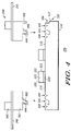
- FIG. 1 illustrates a top view of a semiconductor structure in accordance with an embodiment of the invention
- FIG. 2 illustrates a cross-sectional view of the semiconductor structure in FIG. 1 , as viewed along a section line 2 - 2 in FIG. 1 , in accordance with an embodiment of the invention
- FIG. 3 illustrates an exploded top view of the semiconductor structure in FIG. 1 during a later step of the assembly process in accordance with an embodiment of the invention
- FIG. 4 illustrates a cross-sectional view of the semiconductor structure in FIG. 3 , as viewed along a section line 4 - 4 in FIG. 3 , in accordance with an embodiment of the invention
- FIG. 5 illustrates a top view of the semiconductor structure in FIG. 3 during a later step of the assembly process in accordance with an embodiment of the invention
- FIG. 6 illustrates a cross-sectional view of the semiconductor structure in FIG. 5 , as viewed along a section line 6 - 6 in FIG. 5 , in accordance with an embodiment of the invention
- FIG. 7 illustrates a top view of the semiconductor structure in FIG. 5 during a later step of the assembly process in accordance with an embodiment of the invention
- FIG. 8 illustrates a cross-sectional view of the semiconductor structure in FIG. 7 , as viewed along a section line 8 - 8 in FIG. 7 , in accordance with an embodiment of the invention.
- FIG. 9 illustrates a flow chart of a method of assembling a semiconductor structure or semiconductor packaging system in accordance with an embodiment of the invention.
- Various embodiments of the present invention include a semiconductor structure or semiconductor packaging system and a process of assembly where a substrate or flange has one or more mold lock features for an adhesive.
- the mold lock features are a mechanical reinforcement for an organic adhesive bond between the substrate and an electrical isolator structure and improve the mechanical reliability of the organic adhesive bond.
- the electrical isolator structure also includes one or more protrusions.
- a portion of the electrical isolator structure protrudes into or mates with a recess of the mold lock features, and this mating can inhibit crack propagation along the interface between the organic adhesive and the electrical insulator structure and/or along the interface between the organic adhesive and the substrate.
- the portion of the electrical isolator structure protruding into the recess of the mold lock features can also increase the moisture leak path for ingress to the electronic component or semiconductor structure.
- Input/output leads are also molded or embedded into the plastic insulator frame, which can reduce piece-part costs, improve dimensional tolerances, and enable multiple lead structures.
- the substrate also has an organic adhesive dam and inhibits organic adhesive run-out or ingress.
- the substrate also has an alignment feature to improve the alignment between the substrate and the electrical isolator structure, which, in turn, improves electrical performance of the electronic component or semiconductor structure.
- some embodiments of the invention can include a process of assembly where: (1) a semiconductor chip is attached or coupled to the source flange having one or more mold lock features; (2) the electrical isolator structure with the leads mates with the mold lock features and snaps together with or otherwise couples to the substrate; (3) an organic adhesive between the electrical isolator structure and the substrate is cured to form a strong bond between these two pieces; (4) the semiconductor chip is wire bonded to the leads; and (5) a lid is bonded to the electrical isolator structure to create a hermetic enclosure or at least a gross leak enclosure.
- This process of assembly uses the mold lock features improve the mechanical reliability of the semiconductor structure or semiconductor packaging system. This process also permits the high temperature semiconductor chip or die attach to occur before attaching the electrical insulator structure to the substrate so that the high temperature die attach step does not degrade the bond between the electrical insulator structure and the substrate.
- FIG. 1 illustrates a top view of a semiconductor packaging system or semiconductor structure 100
- FIG. 2 illustrates a cross-sectional view of semiconductor structure 100 as viewed along a section line 2 - 2 in FIG. 1
- Semiconductor structure 100 includes a substrate 110 that has a surface 111 and a surface 112 opposite surface 111 .
- substrate 110 is referred to as a flange.
- substrate 110 serves as a heat sink or heat spreader.
- substrate 110 can comprise a thermally and/or electrically conductive material such as, for example, copper (Cu), copper-based composites, copper-based laminates, aluminum silicon carbide (AlSiC), copper graphite, diamond, and/or the like.
- copper-based composites include copper tungsten (CuW) and copper molybdenum (CuMo), and an example of a copper-based laminate is copper molybdenum copper (CuMoCu).
- mold lock feature 101 can improve the reliability of an organic adhesive-based or other adhesive-based bond between substrate 110 and an electrical isolator structure (also explained below).
- mold lock feature 101 comprises a recess having a rectangular, window-frame shape across surface 111 of substrate 110 and a parallelogram shape into surface 111 of substrate 110 .
- mold lock feature 101 can have a depth of approximately 100-400 micrometers ( ⁇ m) and a width of approximately 200-2,000 ⁇ m.
- Mold lock feature 101 can also be described as comprising four mold lock features or straight grooves coupled together to form a continuous ring, groove, or recess adjacent to a perimeter of substrate 110 .
- the recess of mold lock feature 101 can have other shapes, geometries, depths, and configurations.
- mold lock feature 101 can comprise a multitude of discrete recesses dispersed uniformly or non-uniformly adjacent to the perimeter of substrate 110 .
- the one or more separated recesses of mold lock feature 101 can be formed into substrate 110 during the stamping process used to form substrate 110 .
- Substrate 110 can be part of a lead frame structure or can be an individual element.
- the one or more recesses of mold lock feature 101 can also be one or more through-holes in substrate 110 .
- the recesses can be symmetric or asymmetric with each other.
- mold lock feature 101 can comprise at least one protrusion extending from surface 111 of substrate 110 .
- mold lock feature 101 can be a combination structure comprising one or more recesses and one or more protrusions.
- alignment feature 102 can be used to improve consistency in assembly by improving assembly tolerances, thus enhancing the electrical performance of semiconductor structure 100 .
- alignment feature 102 comprises a recess having a rectangular shape into surface 111 of substrate 110 and having a depth of approximately 100-400 micrometers ( ⁇ m) and a width of approximately 200-1,000 ⁇ m.
- FIG. 1 also illustrates alignment feature 102 comprising two features or grooves coupled together to form a continuous L-shaped groove across surface 111 of substrate 110 and adjacent to the perimeter of substrate 110 at two adjacent sides 116 and 117 of substrate 110 .
- alignment feature 102 forms a portion of side 117 of substrate 110 and a portion of an edge of surface 111 of substrate 110 .
- Alignment feature 102 can also have other shapes, geometries, depths, heights, and configurations, as explained previously for mold lock feature 101 .
- Surface 111 of substrate 110 can also have one or more of optional dams 103 and 104 .
- dams 103 and 104 can be used to inhibit adhesive run-out problems in semiconductor structure 100 and, accordingly, can be referred to as adhesive dams.
- dams 103 and 104 each comprises a recess having a rectangular window-frame shape across surface 111 of substrate 110 and having a triangular shape into surface 111 of substrate 110 .
- dams 103 and 104 can each have a depth of approximately 100-400 micrometers ( ⁇ m) and a width of approximately 200-1,000 ⁇ m.
- each of dams 103 and 104 also illustrates each of dams 103 and 104 to comprise four features or grooves coupled together to form a continuous ring or groove adjacent to the perimeter of substrate 110 .
- Dams 103 and 104 can also have other shapes, geometries, depths, heights, and configurations, as explained previously for mold lock feature 101 .
- substrate 110 has only one of dams 103 and 104 , and in another embodiment of semiconductor structure 100 , substrate does not have any of dams 103 or 104 .
- dams 103 and 104 and mold lock feature 101 can be concentric features. Mold lock feature 101 is located between dams 103 and 104 to prevent an adhesive (described below) from running-out too far across surface 111 of substrate 110 . Dam 104 is located between mold lock feature 101 and a center or central region of substrate 110 where one or more semiconductor chips (described below) are located.
- a portion of surface 111 of substrate 110 can include a layer 113 that overlies the electrically conductive material of substrate 110 .
- Layer 113 can be a metal layer or a solderable metal layer. When layer 113 is a solderable metal layer, layer 113 provides a solderable surface for substrate 110 .
- layer 113 can be a solderable surface comprised of nickel and gold.
- layer 113 can comprise a layer of gold and a layer of nickel between the layer of gold and the electrically conductive material of substrate 110 .
- layer 113 can comprise nickel cobalt (NiCo) and gold (Au).
- layer 113 can be plated onto substrate 110 and can also be located on other surfaces of substrate 110 , including surface 112 .
- layer 113 is located at a first portion of surface 111 of substrate 110 , and layer 113 is absent at a second portion of surface 111 of substrate 110 .
- the first portion can be a central portion of surface 111
- the second portion can be a perimeter portion of surface 111 .
- the perimeter portion of surface 111 is comprised of copper, nickel, or other core materials for substrate 110 that are more conducive to an epoxy or other non-solder adhesive joint, than a gold-based or silver-based surface like layer 113 .
- layer 113 can be selectively plated onto the central portion of surface 111 of substrate 110 such that layer 113 is not contiguous with mold lock feature 101 , alignment feature 102 , or dams 103 and 104 .
- Dam 104 can separate the first portion of surface 111 of substrate 110 from the second portion of surface 111 of substrate 110 .
- dams 103 and 104 , mold lock feature 101 , and alignment feature 102 are located in the second portion of surface 111 of substrate 110 and are devoid of a solderable surface.
- the second portion and thus, dams 103 and 104 , mold lock feature 101 , and alignment feature 102 are located between the first portion and the edges of surface 111 of substrate 110 .
- Substrate 110 can also include optional mounting holes or recesses 114 .
- FIG. 1 depicts two recesses, but the specific quantity of recesses may vary.
- Recesses 114 can be located at opposite sides 115 and 116 of substrate 110 . Recesses 114 can be used to secure semiconductor structure 100 to another substrate such as, for example, a chassis, a heat sink, or a printed circuit board (PC board).
- PC board printed circuit board
- Semiconductor structure 100 also includes at least one semiconductor chip 120 .
- FIG. 1 depicts four semiconductor chips, but the specific quantity of semiconductor chips may vary.
- Semiconductor chips 120 are located over the first portion (i.e., the central portion) of surface 111 of substrate 110 .
- semiconductor chips 120 are comprised of one or more materials suitable for radio frequency or other high frequency devices.
- semiconductor chips 120 are comprised of one or more materials suitable for high power devices.
- semiconductor chips 120 can comprise gallium arsenide (GaAs), silicon, (Si), gallium nitride (GaN), or the like. In most embodiments, semiconductor chips 120 can also be referred to as semiconductor die.
- Each of semiconductor chips 120 includes at least one semiconductor device 121 . Accordingly, semiconductor devices 121 are also located over surface 111 of substrate 110 . At least one of semiconductor devices 121 is an active device (i.e., a transistor) and not merely a passive device (i.e., a resistor, a capacitor, an inductor, etc.). In an embodiment where semiconductor chips 120 are comprised of silicon, semiconductor devices 121 can be laterally diffused metal oxide semiconductor (LDMOS) devices.
- LDMOS laterally diffused metal oxide semiconductor
- At least one of semiconductor devices 121 is an active device (i.e., a transistor) and not merely one or more passive devices (i.e., resistors, capacitors, inductors, etc.), but other ones of semiconductor devices 121 can be matching devices, such as, for example, integrated passive devices (IPDs) and metal-oxide-semiconductor capacitors (MOSCAPs).
- IPDs integrated passive devices
- MOSCAPs metal-oxide-semiconductor capacitors
- one or more of semiconductor chips 120 is replaced with one or more non-semiconductor components that are matching devices. Examples of these non-semiconductor components include IPDs and low temperature co-fired ceramic (LTCC) matching bricks.
- Each of semiconductor chips 120 can have solderable surfaces 122 and 223 comprised of gold (Au), silver (Ag), nickel cobalt gold (NiCoAu), nickel gold (NiAu), or the like. All of surfaces 122 and 223 can be solderable, or only a portion of surfaces 122 and 223 can be solderable. In another embodiment where solder interconnects are not used for semiconductor structure 100 , none of surface 122 is solderable.
- Semiconductor structure 100 also includes an adhesive 230 located between and coupling together semiconductor chips 120 and surface 111 of substrate 110 .
- adhesive 230 can be electrically conductive.
- adhesive 230 can electrically couple semiconductor chips 120 to substrate 110 , which can serve as an electrical lead for semiconductor devices 121 in semiconductor chips 120 .
- substrate 110 can be referred to as a source substrate or source flange when substrate 110 is an electrical lead for a source electrode of semiconductor devices 121 .
- adhesive 230 includes several discrete or individualized portions.
- adhesive 230 can be any suitable chip or die attach material such as a lead-based or non-lead-based solder.
- adhesive 230 can be referred to as a solder element.
- suitable non-lead-based solders include gold tin (AuSn), gold silicon (AuSi), or the like.
- adhesive 230 solders together a portion of layer 113 at surface 111 and surface 223 .
- adhesive 230 can be comprised of a material with a low coefficient of thermal expansion (CTE) such as gold silicon to more closely match the CTE of semiconductor chips 120 .
- adhesive 230 can be an electrically conductive or non-electrically conductive epoxy or a thermoset or thermoplastic polymer.
- Adhesive 230 can be formed on solderable surface 223 of semiconductor chips 120 or on layer 113 of surface 111 of substrate 110 using cladding, plating, screen printing, or solder ball techniques. Adhesive 230 can also be a perform. As explained below, adhesive 230 can also have a melting temperature and a reflow temperature that are higher than melting and reflow temperatures for other adhesives, or solders, that are used during later stages of the manufacturing or assembly process for semiconductor structure 100 .
- FIG. 3 illustrates an exploded top view of semiconductor structure 100 during a later step of the assembly process
- FIG. 4 illustrates a cross-sectional view of semiconductor structure 100 as viewed along a section line 4 - 4 in FIG. 3
- Semiconductor structure 100 additionally includes an electrical isolator structure 340 located over surface 111 of substrate 110 .
- electrical isolator structure 340 includes two electrical leads 341 and 342 .
- electrical isolator structure 340 can include more or less than two electrical leads.
- Electrical leads 341 and 342 are used to conduct electrical signals to and from semiconductor devices 121 in semiconductor chips 120 and into and out of semiconductor structure 100 .
- electrical leads 341 and 342 can be gate and drain leads, respectively, for gate and drain electrodes of semiconductor devices 121 .
- substrate 110 can serve as a source lead for source electrodes of semiconductor devices 121 .
- electrical leads 341 and 342 can comprise electrically conductive materials including, for example, copper, a copper alloy, and other electrically conductive materials identified previously for substrate 110 . Additionally, electrical leads 341 and 342 can comprise an iron-based alloy with nickel such as, for example, Alloy 42 , whose composition comprises forty-two percent nickel. Electrical leads 341 and 342 can also comprise an iron-based alloy with nickel and cobalt, as sold under the brand name Kovar® by CRS Holdings, Inc., a Delaware corporation.
- Electrical leads 341 and 342 can also include a solderable surface to make electrical leads 341 and 342 suitable for wire bonding or other interconnect schemes inside of semiconductor structure 100 and to make electrical leads 341 and 342 suitable for wire bonding or soldering outside of semiconductor structure 100 .
- the solderable surface of electrical leads 341 and 342 can comprise the same solderable materials identified for layer 113 of substrate 110 ( FIGS. 1 and 2 ) and solderable surfaces 122 and 223 of semiconductor chips 120 .
- Electrical isolator structure 340 also includes an organic-based element 343 molded to electrical leads 341 and 342 .
- organic-based element 343 can have the shape of a window frame, as illustrated in FIG. 3 .
- organic-based element 343 can be referred to as a frame, and electrical isolator structure 340 can be referred to as a frame structure.
- Organic-based element is comprised of an electrically insulative material such as, for example, a polymer, a thermoplastic, and/or a thermoset material. Accordingly, in some embodiments, organic-based element 343 can also be referred to as a plastic insulator frame.
- Organic-based element 343 can be formed by using an injection, transfer, or other molding process to mold organic-based element 343 to electrical leads 341 and 342 .
- the portion of organic-based element 343 located over leads 341 and 342 is optional and can be eliminated in some embodiments of semiconductor structure 100 .
- Electrical isolator structure 340 also includes an optional portion 444 over surface 111 of substrate 110 .
- Portion 444 is optional such that some embodiments of electrical isolator structure 340 do not include portion 444 .
- portion 444 is a portion of organic-based element 343 , but in other embodiments, portion 444 can be separate from organic-based element 343 .
- portion 444 is a protrusion from organic-based element 343 that is designed to mate with mold lock feature 101 in substrate 110 .
- portion 444 can comprise four protrusions coupled together to form a continuous window-frame shaped protrusion adjacent to the perimeter of substrate 110 and to a perimeter of organic-based element 343 .
- mold lock feature 101 is a protrusion from surface 111 of substrate 110
- the shape, configuration, geometry, and size of portion 444 can be modified accordingly such that portion 444 still mates with mold lock feature 101 .
- portion 444 is conformal to the shape, configuration, geometry, and size of mold lock feature 101 , but in other embodiments, portion 444 can have different shapes, configurations, geometries, and/or sizes and still mate with mold lock feature 101 .
- portion 444 can be a set of discrete protrusions adjacent to the perimeters of substrate 110 and organic-based element 343 .
- portion 444 can have a parallelogram cross-section, a pentagon cross-section, a triangular cross-section, or a semi-circular cross-section.
- portion 444 snaps together with mold lock feature 101 and anchors electrical isolator structure 340 to substrate 110 .
- portion 444 has a tight fit with mold lock feature 101 .
- portion 444 can be conformal or non-conformal to mold lock feature 101 .
- Electrical isolator structure 340 further includes an optional portion 445 over surface 111 of substrate 110 .
- Portion 445 is optional such that some embodiments of electrical isolator structure 340 do not include portion 445 .
- the bottom surface of organic-based element 343 can be smooth or planar.
- portion 445 is also a portion of organic-based element 343 , but in other embodiments, portion 445 can be separate from organic-based element 343 .
- portion 445 is a protrusion from organic-based element 343 that is designed to mate with alignment feature 102 in substrate 110 . Accordingly, when alignment feature 102 comprises two grooves coupled together to form an continuous L-shaped groove across surface 111 of substrate 110 , then portion 445 can comprise two protrusions coupled together to form a continuous L-shaped protrusion across surface 111 of substrate 110 and across organic-based element 343 .
- alignment feature 102 is a protrusion from surface 111 of substrate 110
- the shape, configuration, geometry, and size of portion 445 can be modified accordingly such that portion 445 still mates with alignment feature 102 .
- portion 445 relative to alignment feature 102 can be similar to the previously described characteristics of portion 444 relative to mold lock feature 101 , except that portion 445 and alignment feature 102 aid in the alignment of electrical isolator structure 340 to substrate 110 while portion 444 and mold lock feature 101 aid in forming a reliable joint between electrical isolator structure 340 and substrate 110 .
- alignment feature 102 and portion 445 can be eliminated where mold lock feature 101 and portion 444 provide both functions of alignment and increased joint reliability.
- Semiconductor structure 100 also includes an adhesive element 450 .
- Adhesive element 450 is located between electrical isolator structure 340 and surface 111 of substrate 110 , and adhesive element 450 couples together electrical isolator structure 340 and substrate 110 . More specifically, adhesive element 450 adheres together surface 111 of substrate 110 and organic-based element 343 of electrical isolator structure 340 .
- adhesive element 450 can comprise an epoxy material or other organic adhesives such as silicone, a pressure adhesive, or other thermoset or thermoplastic adhesives.
- Adhesive element 450 can have a shape similar to the window frame shape of organic-based element 343 .
- adhesive element 450 Prior to being activated, adhesive element 450 can be comprised of a single piece, or it can be comprised of two or more discrete pieces. If adhesive element 450 originates as two or more discrete pieces, the step of melting, reflowing, or activating adhesive element 450 preferably combines the pieces so that adhesive element 450 becomes a single, unitary element.
- adhesive element 450 is illustrated to be deposited on and adjacent to portion 444 of electrical isolator structure 340 .
- adhesive element 450 can be deposited on the entire bottom surface of electrical isolator structure 340 , including on portion 445 of electrical isolator structure 340 .
- adhesive element 450 can be deposited on a portion of surface 111 of substrate 110 .
- adhesive element 450 can be deposited on surface 111 before or after semiconductor chips 120 are attached or bonded to substrate 110 .
- adhesive element 450 can be deposited only in mold lock feature 101 .
- FIG. 5 illustrates a top view of semiconductor structure 100 during an even later step of the assembly process
- FIG. 6 illustrates a cross-sectional view of semiconductor structure 100 as viewed along a section line 6 - 6 in FIG. 5
- FIG. 6 several portions of electrical isolator structure 340 are mated with substrate 110 .
- portion 444 of electrical isolator structure 340 is mated with and located in mold lock feature 101 .
- portion 445 of electrical isolator structure 340 is mated with and located in alignment feature 102 .
- Portion 445 and alignment feature 102 provide more precise alignment of electrical isolator structure 340 and substrate 110 relative to each other, which can improve the electrical performance of semiconductor structure 100 .
- mold locks have been used in other semiconductor components, those other semiconductor components mold a polymer-based frame directly to the substrate. Accordingly, the mold locks are used for and during the molding process.
- mold lock feature 101 are not used for or during a molding process to create electrical isolator structure 340 or to couple electrical isolator structure 340 to substrate 110 .
- mold lock feature 101 and portions 444 are used in an adhesive-attach or an epoxy-attach process. In particular, mold lock feature 101 and portions 444 mechanically couple together electrical isolator structure 340 and substrate 110 and/or mechanically reinforce the interface between electrical isolator structure 340 and substrate 110 .
- adhesive element 450 adheres electrical isolator structure 340 to substrate 110 and vice versa.
- Adhesive element 450 chemically couples together electrical isolator structure 340 and substrate 110 .
- portion 444 of electrical isolator structure 340 is smaller than mold lock feature 101 such that a portion of adhesive element 450 is also located in mold lock feature 101 .
- portion 444 can be smaller than mold lock feature 101 in the vertical direction or z-axis perpendicular to surface 111 of substrate 110 , and/or portion 444 can be smaller than mold lock feature 101 in the horizontal direction or x- and/or y-axes parallel to surface 111 of substrate 110 .
- portion 444 in mold lock feature 101 can allow adhesive element 450 to seep or wick into mold lock feature 101 during the manufacturing or assembly of semiconductor structure 100 .
- a portion of adhesive element 450 is also located in dams 103 and 104 .
- adhesive element 450 stops at dashed lines 650 and within dams 103 and 104 .
- dams 103 and 104 inhibit adhesive run-out towards the perimeter of substrate 110 and towards semiconductor chips 120 , respectively.
- the process of coupling together electrical isolator structure 340 and substrate 110 can be performed in a vacuum to enhance the flow of adhesive element 450 into mold lock feature 101 and dams 103 and 104 .
- adhesive element 450 can also be located in alignment feature 102 .
- Semiconductor structure 100 additionally includes wire bonds 560 electrically coupling together semiconductor devices 121 in semiconductor chips 120 and electrical leads 341 and 342 .
- wire bonds 560 comprise electrically conductive materials, as known in the art, such as, for example, gold, aluminum silicon, aluminum manganese, copper, lead-based solders such as lead tin silver, or the like.
- wire bonds 560 are replaced with other electrical interconnect structures such as, for example, solder balls, flip-chip interconnects, tape automated bonding,(TAB), and the like.
- FIG. 7 illustrates a top view of semiconductor structure 100 during a subsequent step of the assembly process
- FIG. 8 illustrates a cross-sectional view of semiconductor structure 100 as viewed along a section line 8 - 8 in FIG. 7
- Semiconductor structure 100 includes a lid 770 located over substrate 110 , semiconductor chips 120 , and electrical isolator structure 340 .
- Lid 770 protects semiconductor chips 120 and wire bonds 560 from physical and environmental damage.
- Lid 770 can be coupled to organic-based element 343 and/or electrical leads 341 and 342 .
- lid 770 can be comprised of a liquid crystal polymer (LCP), ceramic, or other non-electrically conductive material.
- Lid 770 can have many different configurations, including a recess to accommodate higher wire bonds.
- Substrate 110 , organic-based element 343 of electrically isolated structure 340 , electrical leads 341 and 342 of electrically isolated structure 340 , adhesive element 450 , and lid 770 form at least a gross leakage sealed package having an air gap 880 in which semiconductor chips 120 and wire bonds 560 are located.
- semiconductor structure 100 is a hermetically sealed package.
- semiconductor devices 121 in semiconductor chips 120 are high power, radio frequency devices so the package is a high power, radio frequency package.
- air gap 880 can be comprised of other materials such as, for example, nitrogen or another inert gas.
- FIG. 9 illustrates a flow chart 900 of a method of assembling a semiconductor structure.
- the semiconductor structure of flow chart 900 can be similar to semiconductor packaging system or semiconductor structure 100 of FIGS. 1-8 and all of its various embodiments.
- Flow chart 900 includes a step 901 for providing a substrate having a surface and at least one mold lock feature.
- the substrate of step 901 can be similar to substrate 110 in FIGS. 1 and 2
- the surface and the mold lock feature of step 901 can be similar to surface 111 and mold lock feature 101 in FIGS. 1 and 2 .
- the substrate of step 901 can also include one or more dams, which can be similar to dams 103 and 104 in FIGS. 1 and 2 .
- the substrate of step 901 can include one or more alignment features, which can be similar to alignment feature 102 in FIGS. 1 and 2 .
- Flow chart 900 continues with a step 902 for using an adhesive to mount at least one semiconductor chip over the surface of the substrate.
- the adhesive and the semiconductor chip of step 902 can be similar to semiconductor chips 120 and adhesive 230 , respectively, in FIGS. 1 and 2 .
- step 902 can include mounting the matching element(s) to or over the surface of the substrate.
- the matching element(s) can be mounted before, simultaneously with, or after the semiconductor chip(s).
- step 903 for using an adhesive to mount an electrical isolator structure over the surface of the substrate, where a portion of the electrical isolator structure is located in the at least one mold lock feature.
- Step 903 can include mating and/or snapping the portion of the electrical isolator structure into the at least one mold lock feature, as explained previously with respect to FIG. 4 .
- the adhesive and the electrical isolator structure in step 902 can be similar to adhesive element 450 and electrical isolator structure 340 , respectively, in FIGS. 3 and 4 . Additionally, the portion of the electrical isolator structure in step 902 can be similar to portion 444 of electrical isolator structure 340 in FIG. 4 . As explained previously with respect to FIG. 6 , a portion of the adhesive in step 903 can be located in the at least one mold lock feature. In an embodiment where the substrate includes one or more dams, the dams can prevent or at least inhibit run-out problems for the adhesive of step 903 . In an. embodiment where the substrate of step 901 includes an alignment feature, step 902 can include mating a portion of the electrical isolator structure with, or positioning a portion of the electrical isolator structure in, the alignment feature.
- step 904 for electrically coupling the semiconductor chip to the electrical isolator structure.
- wire bonds 560 and other the interconnect structures described with reference to FIGS. 5 and 6 can be used during step 904 to electrically couple the semiconductor device of the semiconductor chip to the electrical leads of the electrical isolator structure.
- Flow chart 900 also includes a step 905 for attaching a lid to the electrical isolator structure to seal the at least one semiconductor chip therein.
- the lid of step 905 can be similar to lid 770 in FIGS. 7 and 8 .
- the lid hermetically or at least gross leak seals the semiconductor chip within the semiconductor structure.
- step 905 can use epoxy or other adhesives to attach the lid to the electrical isolator structure, or step 904 can use sonic, ultrasonic, thermal, or other welding techniques to accomplish the same.
- step 905 can attach the lid to the surface of the substrate.
- step 905 can be performed simultaneously with step 903 , or step 905 can be performed prior to step 903 .
- adhesive element 450 can be comprised of a solder material.
- embodiments and limitations disclosed herein are not dedicated to the public under the doctrine of dedication if the embodiments and/or limitations: (1) are not expressly claimed in the claims; and (2) are or are potentially equivalents of express elements and/or limitations in the claims under the doctrine of equivalents.
Abstract
Description
Claims (27)
Priority Applications (1)
| Application Number | Priority Date | Filing Date | Title |
|---|---|---|---|
| US11/257,783 US7429790B2 (en) | 2005-10-24 | 2005-10-24 | Semiconductor structure and method of manufacture |
Applications Claiming Priority (1)
| Application Number | Priority Date | Filing Date | Title |
|---|---|---|---|
| US11/257,783 US7429790B2 (en) | 2005-10-24 | 2005-10-24 | Semiconductor structure and method of manufacture |
Publications (2)
| Publication Number | Publication Date |
|---|---|
| US20070090514A1 US20070090514A1 (en) | 2007-04-26 |
| US7429790B2 true US7429790B2 (en) | 2008-09-30 |
Family
ID=37984586
Family Applications (1)
| Application Number | Title | Priority Date | Filing Date |
|---|---|---|---|
| US11/257,783 Active 2026-06-11 US7429790B2 (en) | 2005-10-24 | 2005-10-24 | Semiconductor structure and method of manufacture |
Country Status (1)
| Country | Link |
|---|---|
| US (1) | US7429790B2 (en) |
Cited By (20)
| Publication number | Priority date | Publication date | Assignee | Title |
|---|---|---|---|---|
| US20090236616A1 (en) * | 2008-03-19 | 2009-09-24 | Foxconn Technology Co., Ltd. | Led assembly with separated thermal and electrical structures thereof |
| US20100084762A1 (en) * | 2006-04-21 | 2010-04-08 | Hidenobu Nishikawa | Memory card |
| US20110115067A1 (en) * | 2009-11-18 | 2011-05-19 | Jen-Chung Chen | Semiconductor chip package with mold locks |
| US20110117232A1 (en) * | 2009-11-18 | 2011-05-19 | Jen-Chung Chen | Semiconductor chip package with mold locks |
| US8269244B2 (en) | 2010-06-28 | 2012-09-18 | Cree, Inc. | LED package with efficient, isolated thermal path |
| USD679842S1 (en) | 2011-01-03 | 2013-04-09 | Cree, Inc. | High brightness LED package |
| US8598602B2 (en) | 2009-01-12 | 2013-12-03 | Cree, Inc. | Light emitting device packages with improved heat transfer |
| US8610140B2 (en) | 2010-12-15 | 2013-12-17 | Cree, Inc. | Light emitting diode (LED) packages, systems, devices and related methods |
| US8648359B2 (en) | 2010-06-28 | 2014-02-11 | Cree, Inc. | Light emitting devices and methods |
| US8860043B2 (en) | 2009-06-05 | 2014-10-14 | Cree, Inc. | Light emitting device packages, systems and methods |
| US20150092379A1 (en) * | 2013-09-30 | 2015-04-02 | Mitsubishi Electric Corporation | Semiconductor device and method for manufacturing the same |
| US20150146399A1 (en) * | 2013-11-25 | 2015-05-28 | Lakshminarayan Viswanathan | Packaged semiconductor devices and methods of their fabrication |
| US9240390B2 (en) | 2013-06-27 | 2016-01-19 | Freescale Semiconductor, Inc. | Semiconductor packages having wire bond wall to reduce coupling |
| US9312817B2 (en) | 2012-07-20 | 2016-04-12 | Freescale Semiconductor, Inc. | Semiconductor package design providing reduced electromagnetic coupling between circuit components |
| US20160192535A1 (en) * | 2014-12-26 | 2016-06-30 | Denso Corporation | Electronic device and actuator using the same |
| US9401342B2 (en) | 2013-06-27 | 2016-07-26 | Freescale Semiconductor, Inc. | Semiconductor package having wire bond wall to reduce coupling |
| US9698116B2 (en) | 2014-10-31 | 2017-07-04 | Nxp Usa, Inc. | Thick-silver layer interface for a semiconductor die and corresponding thermal layer |
| US10199302B1 (en) | 2017-08-07 | 2019-02-05 | Nxp Usa, Inc. | Molded air cavity packages and methods for the production thereof |
| US10629518B2 (en) | 2018-08-29 | 2020-04-21 | Nxp Usa, Inc. | Internally-shielded microelectronic packages and methods for the fabrication thereof |
| US10998255B2 (en) | 2018-07-12 | 2021-05-04 | Nxp Usa, Inc. | Overmolded microelectronic packages containing knurled flanges and methods for the production thereof |
Families Citing this family (13)
| Publication number | Priority date | Publication date | Assignee | Title |
|---|---|---|---|---|
| US8039947B2 (en) * | 2006-05-17 | 2011-10-18 | Stats Chippac Ltd. | Integrated circuit package system with different mold locking features |
| WO2011119891A2 (en) * | 2010-03-25 | 2011-09-29 | Anwar Abdul Mohammed | High performance low cost open air cavity ceramic power packages for high temperature die attach processes |
| JP5602095B2 (en) * | 2011-06-09 | 2014-10-08 | 三菱電機株式会社 | Semiconductor device |
| US8698291B2 (en) | 2011-12-15 | 2014-04-15 | Freescale Semiconductor, Inc. | Packaged leadless semiconductor device |
| US8803302B2 (en) * | 2012-05-31 | 2014-08-12 | Freescale Semiconductor, Inc. | System, method and apparatus for leadless surface mounted semiconductor package |
| CN103151317B (en) * | 2013-02-21 | 2015-12-23 | 日月光半导体制造股份有限公司 | Semiconductor package and manufacture method thereof |
| DE102013220880B4 (en) * | 2013-10-15 | 2016-08-18 | Infineon Technologies Ag | An electronic semiconductor package having an electrically insulating, thermal interface structure on a discontinuity of an encapsulation structure, and a manufacturing method therefor, and an electronic device having the same |
| US20150257300A1 (en) * | 2014-03-10 | 2015-09-10 | Kabushiki Kaisha Toshiba | Electronic device |
| WO2015179733A1 (en) * | 2014-05-23 | 2015-11-26 | Materion Corporation | Air cavity package |
| US9859185B2 (en) * | 2016-01-28 | 2018-01-02 | Kyocera International, Inc. | Semiconductor packaging structure and package having stress release structure |
| WO2017201260A1 (en) * | 2016-05-20 | 2017-11-23 | Materion Corporation | Copper flanged air cavity packages for high frequency devices |
| NL2022669B1 (en) * | 2019-03-01 | 2020-09-15 | Ampleon Netherlands Bv | Packaged electronic device |
| WO2020261730A1 (en) * | 2019-06-25 | 2020-12-30 | Ngkエレクトロデバイス株式会社 | Package, and method for manufacturing power semiconductor module |
Citations (16)
| Publication number | Priority date | Publication date | Assignee | Title |
|---|---|---|---|---|
| US3778887A (en) * | 1970-12-23 | 1973-12-18 | Hitachi Ltd | Electronic devices and method for manufacturing the same |
| US4994897A (en) * | 1989-10-26 | 1991-02-19 | Motorola, Inc. | Multi-level semiconductor package |
| US5138430A (en) * | 1991-06-06 | 1992-08-11 | International Business Machines Corporation | High performance versatile thermally enhanced IC chip mounting |
| US5278446A (en) * | 1992-07-06 | 1994-01-11 | Motorola, Inc. | Reduced stress plastic package |
| US5378924A (en) * | 1992-09-10 | 1995-01-03 | Vlsi Technology, Inc. | Apparatus for thermally coupling a heat sink to a lead frame |
| JPH09107059A (en) * | 1995-10-11 | 1997-04-22 | Toshiba Corp | Semiconductor device and manufacture thereof |
| US5701034A (en) * | 1994-05-03 | 1997-12-23 | Amkor Electronics, Inc. | Packaged semiconductor die including heat sink with locking feature |
| US6072238A (en) | 1999-04-07 | 2000-06-06 | Motorola, Inc. | Semiconductor component |
| US6072211A (en) | 1998-08-03 | 2000-06-06 | Motorola, Inc. | Semiconductor package |
| US6261868B1 (en) | 1999-04-02 | 2001-07-17 | Motorola, Inc. | Semiconductor component and method for manufacturing the semiconductor component |
| US6511866B1 (en) | 2001-07-12 | 2003-01-28 | Rjr Polymers, Inc. | Use of diverse materials in air-cavity packaging of electronic devices |
| US6713849B2 (en) * | 2000-12-28 | 2004-03-30 | Hitachi, Ltd. | Semiconductor utilizing grooves in lead and tab portions of lead frame to prevent peel off between the lead frame and the resin |
| US6867367B2 (en) | 2003-01-29 | 2005-03-15 | Quantum Leap Packaging, Inc. | Package for integrated circuit die |
| US6943433B2 (en) * | 2002-03-06 | 2005-09-13 | Nichia Corporation | Semiconductor device and manufacturing method for same |
| US20060108673A1 (en) * | 2003-06-27 | 2006-05-25 | Germain Stephen S | Method for forming an encapsulated device and structure |
| US7224047B2 (en) * | 2004-12-18 | 2007-05-29 | Lsi Corporation | Semiconductor device package with reduced leakage |
-
2005
- 2005-10-24 US US11/257,783 patent/US7429790B2/en active Active
Patent Citations (16)
| Publication number | Priority date | Publication date | Assignee | Title |
|---|---|---|---|---|
| US3778887A (en) * | 1970-12-23 | 1973-12-18 | Hitachi Ltd | Electronic devices and method for manufacturing the same |
| US4994897A (en) * | 1989-10-26 | 1991-02-19 | Motorola, Inc. | Multi-level semiconductor package |
| US5138430A (en) * | 1991-06-06 | 1992-08-11 | International Business Machines Corporation | High performance versatile thermally enhanced IC chip mounting |
| US5278446A (en) * | 1992-07-06 | 1994-01-11 | Motorola, Inc. | Reduced stress plastic package |
| US5378924A (en) * | 1992-09-10 | 1995-01-03 | Vlsi Technology, Inc. | Apparatus for thermally coupling a heat sink to a lead frame |
| US5701034A (en) * | 1994-05-03 | 1997-12-23 | Amkor Electronics, Inc. | Packaged semiconductor die including heat sink with locking feature |
| JPH09107059A (en) * | 1995-10-11 | 1997-04-22 | Toshiba Corp | Semiconductor device and manufacture thereof |
| US6072211A (en) | 1998-08-03 | 2000-06-06 | Motorola, Inc. | Semiconductor package |
| US6261868B1 (en) | 1999-04-02 | 2001-07-17 | Motorola, Inc. | Semiconductor component and method for manufacturing the semiconductor component |
| US6072238A (en) | 1999-04-07 | 2000-06-06 | Motorola, Inc. | Semiconductor component |
| US6713849B2 (en) * | 2000-12-28 | 2004-03-30 | Hitachi, Ltd. | Semiconductor utilizing grooves in lead and tab portions of lead frame to prevent peel off between the lead frame and the resin |
| US6511866B1 (en) | 2001-07-12 | 2003-01-28 | Rjr Polymers, Inc. | Use of diverse materials in air-cavity packaging of electronic devices |
| US6943433B2 (en) * | 2002-03-06 | 2005-09-13 | Nichia Corporation | Semiconductor device and manufacturing method for same |
| US6867367B2 (en) | 2003-01-29 | 2005-03-15 | Quantum Leap Packaging, Inc. | Package for integrated circuit die |
| US20060108673A1 (en) * | 2003-06-27 | 2006-05-25 | Germain Stephen S | Method for forming an encapsulated device and structure |
| US7224047B2 (en) * | 2004-12-18 | 2007-05-29 | Lsi Corporation | Semiconductor device package with reduced leakage |
Cited By (32)
| Publication number | Priority date | Publication date | Assignee | Title |
|---|---|---|---|---|
| US20100084762A1 (en) * | 2006-04-21 | 2010-04-08 | Hidenobu Nishikawa | Memory card |
| US8599571B2 (en) * | 2006-04-21 | 2013-12-03 | Panasonic Corporation | Memory card |
| US7795628B2 (en) * | 2008-03-19 | 2010-09-14 | Foxconn Technology Co., Ltd. | LED assembly with separated thermal and electrical structures thereof |
| US20090236616A1 (en) * | 2008-03-19 | 2009-09-24 | Foxconn Technology Co., Ltd. | Led assembly with separated thermal and electrical structures thereof |
| US8598602B2 (en) | 2009-01-12 | 2013-12-03 | Cree, Inc. | Light emitting device packages with improved heat transfer |
| US8860043B2 (en) | 2009-06-05 | 2014-10-14 | Cree, Inc. | Light emitting device packages, systems and methods |
| US20110115067A1 (en) * | 2009-11-18 | 2011-05-19 | Jen-Chung Chen | Semiconductor chip package with mold locks |
| US20110117232A1 (en) * | 2009-11-18 | 2011-05-19 | Jen-Chung Chen | Semiconductor chip package with mold locks |
| US8269244B2 (en) | 2010-06-28 | 2012-09-18 | Cree, Inc. | LED package with efficient, isolated thermal path |
| US8878217B2 (en) | 2010-06-28 | 2014-11-04 | Cree, Inc. | LED package with efficient, isolated thermal path |
| US8648359B2 (en) | 2010-06-28 | 2014-02-11 | Cree, Inc. | Light emitting devices and methods |
| US8610140B2 (en) | 2010-12-15 | 2013-12-17 | Cree, Inc. | Light emitting diode (LED) packages, systems, devices and related methods |
| USD679842S1 (en) | 2011-01-03 | 2013-04-09 | Cree, Inc. | High brightness LED package |
| US9312817B2 (en) | 2012-07-20 | 2016-04-12 | Freescale Semiconductor, Inc. | Semiconductor package design providing reduced electromagnetic coupling between circuit components |
| US9240390B2 (en) | 2013-06-27 | 2016-01-19 | Freescale Semiconductor, Inc. | Semiconductor packages having wire bond wall to reduce coupling |
| US9978691B2 (en) | 2013-06-27 | 2018-05-22 | Nxp Usa, Inc. | Semiconductor packages having wire bond wall to reduce coupling |
| US9401342B2 (en) | 2013-06-27 | 2016-07-26 | Freescale Semiconductor, Inc. | Semiconductor package having wire bond wall to reduce coupling |
| US20150092379A1 (en) * | 2013-09-30 | 2015-04-02 | Mitsubishi Electric Corporation | Semiconductor device and method for manufacturing the same |
| US10104775B2 (en) * | 2013-09-30 | 2018-10-16 | Mitsubishi Electric Corporation | Semiconductor device and method for manufacturing the same |
| US20150146399A1 (en) * | 2013-11-25 | 2015-05-28 | Lakshminarayan Viswanathan | Packaged semiconductor devices and methods of their fabrication |
| US9099567B2 (en) * | 2013-11-25 | 2015-08-04 | Freescale Semiconductor, Inc. | Packaged semiconductor devices and methods of their fabrication |
| US9425161B2 (en) | 2013-11-25 | 2016-08-23 | Freescale Semiconductor, Inc. | Semiconductor device with mechanical lock features between a semiconductor die and a substrate |
| US9698116B2 (en) | 2014-10-31 | 2017-07-04 | Nxp Usa, Inc. | Thick-silver layer interface for a semiconductor die and corresponding thermal layer |
| CN105744801A (en) * | 2014-12-26 | 2016-07-06 | 株式会社电装 | Electronic device and actuator using the same |
| US20160192535A1 (en) * | 2014-12-26 | 2016-06-30 | Denso Corporation | Electronic device and actuator using the same |
| US10211707B2 (en) * | 2014-12-26 | 2019-02-19 | Denso Corporation | Electronic device and actuator using the same |
| CN105744801B (en) * | 2014-12-26 | 2019-11-15 | 株式会社电装 | Electronic device and the actuator for using the electronic device |
| US10199302B1 (en) | 2017-08-07 | 2019-02-05 | Nxp Usa, Inc. | Molded air cavity packages and methods for the production thereof |
| US10396006B2 (en) | 2017-08-07 | 2019-08-27 | Nxp Usa, Inc. | Molded air cavity packages and methods for the production thereof |
| US10529638B2 (en) | 2017-08-07 | 2020-01-07 | Nxp Usa, Inc. | Molded air cavity packages and methods for the production thereof |
| US10998255B2 (en) | 2018-07-12 | 2021-05-04 | Nxp Usa, Inc. | Overmolded microelectronic packages containing knurled flanges and methods for the production thereof |
| US10629518B2 (en) | 2018-08-29 | 2020-04-21 | Nxp Usa, Inc. | Internally-shielded microelectronic packages and methods for the fabrication thereof |
Also Published As
| Publication number | Publication date |
|---|---|
| US20070090514A1 (en) | 2007-04-26 |
Similar Documents
| Publication | Publication Date | Title |
|---|---|---|
| US7429790B2 (en) | Semiconductor structure and method of manufacture | |
| US7446411B2 (en) | Semiconductor structure and method of assembly | |
| US5578869A (en) | Components for housing an integrated circuit device | |
| TWI588919B (en) | Semiconductor package structure and manufacturing method thereof | |
| US7217594B2 (en) | Alternative flip chip in leaded molded package design and method for manufacture | |
| US7268426B2 (en) | High-frequency chip packages | |
| CN1717156B (en) | Electronic component packaging method, semiconductor module, and semiconductor device | |
| TWI469280B (en) | Semiconductor component and method of manufacture | |
| EP0933816A2 (en) | Hybrid module and methods for manufacturing and mounting thereof | |
| US8129225B2 (en) | Method of manufacturing an integrated circuit module | |
| US20120175755A1 (en) | Semiconductor device including a heat spreader | |
| US20140063757A1 (en) | Joint structure of package members, method for joining same, and package | |
| KR20170086828A (en) | Clip -bonded semiconductor chip package using metal bump and the manufacturing method thereof | |
| US20120235293A1 (en) | Semiconductor device including a base plate | |
| US20090127677A1 (en) | Multi-Terminal Package Assembly For Semiconductor Devices | |
| TW200416981A (en) | Package for housing semiconductor chip, and semiconductor device | |
| KR20020095053A (en) | Power module package improved heat radiating capability and method for manufacturing the same | |
| US20240096734A1 (en) | Leadframe spacer for double-sided power module | |
| US20050046035A1 (en) | Semiconductor device | |
| JP4412072B2 (en) | Electronic component mounting method, semiconductor module, and semiconductor device | |
| JP3816821B2 (en) | High frequency power module substrate and manufacturing method thereof | |
| WO1996030942A1 (en) | Components for housing an integrated circuit device | |
| JP4608409B2 (en) | High heat dissipation type electronic component storage package | |
| WO2012026516A1 (en) | Element-containing package and module provided therewith | |
| JP2017188635A (en) | Heat spreader structure element for power module |
Legal Events
| Date | Code | Title | Description |
|---|---|---|---|
| AS | Assignment |
Owner name: FREESCALE SEMICONDUCTOR, INC., TEXAS Free format text: ASSIGNMENT OF ASSIGNORS INTEREST;ASSIGNORS:CONDIE, BRIAN W.;VISWANATHAN, LAKSHMINARAYAN;WETZ, RICHARD W.;REEL/FRAME:017653/0084 Effective date: 20051021 |
|
| AS | Assignment |
Owner name: CITIBANK, N.A. AS COLLATERAL AGENT, NEW YORK Free format text: SECURITY AGREEMENT;ASSIGNORS:FREESCALE SEMICONDUCTOR, INC.;FREESCALE ACQUISITION CORPORATION;FREESCALE ACQUISITION HOLDINGS CORP.;AND OTHERS;REEL/FRAME:018855/0129 Effective date: 20061201 Owner name: CITIBANK, N.A. AS COLLATERAL AGENT,NEW YORK Free format text: SECURITY AGREEMENT;ASSIGNORS:FREESCALE SEMICONDUCTOR, INC.;FREESCALE ACQUISITION CORPORATION;FREESCALE ACQUISITION HOLDINGS CORP.;AND OTHERS;REEL/FRAME:018855/0129 Effective date: 20061201 |
|
| STCF | Information on status: patent grant |
Free format text: PATENTED CASE |
|
| AS | Assignment |
Owner name: CITIBANK, N.A., AS COLLATERAL AGENT,NEW YORK Free format text: SECURITY AGREEMENT;ASSIGNOR:FREESCALE SEMICONDUCTOR, INC.;REEL/FRAME:024397/0001 Effective date: 20100413 Owner name: CITIBANK, N.A., AS COLLATERAL AGENT, NEW YORK Free format text: SECURITY AGREEMENT;ASSIGNOR:FREESCALE SEMICONDUCTOR, INC.;REEL/FRAME:024397/0001 Effective date: 20100413 |
|
| FPAY | Fee payment |
Year of fee payment: 4 |
|
| AS | Assignment |
Owner name: CITIBANK, N.A., AS NOTES COLLATERAL AGENT, NEW YOR Free format text: SECURITY AGREEMENT;ASSIGNOR:FREESCALE SEMICONDUCTOR, INC.;REEL/FRAME:030633/0424 Effective date: 20130521 |
|
| AS | Assignment |
Owner name: CITIBANK, N.A., AS NOTES COLLATERAL AGENT, NEW YOR Free format text: SECURITY AGREEMENT;ASSIGNOR:FREESCALE SEMICONDUCTOR, INC.;REEL/FRAME:031591/0266 Effective date: 20131101 |
|
| AS | Assignment |
Owner name: FREESCALE SEMICONDUCTOR, INC., TEXAS Free format text: PATENT RELEASE;ASSIGNOR:CITIBANK, N.A., AS COLLATERAL AGENT;REEL/FRAME:037354/0225 Effective date: 20151207 Owner name: FREESCALE SEMICONDUCTOR, INC., TEXAS Free format text: PATENT RELEASE;ASSIGNOR:CITIBANK, N.A., AS COLLATERAL AGENT;REEL/FRAME:037356/0143 Effective date: 20151207 Owner name: FREESCALE SEMICONDUCTOR, INC., TEXAS Free format text: PATENT RELEASE;ASSIGNOR:CITIBANK, N.A., AS COLLATERAL AGENT;REEL/FRAME:037356/0553 Effective date: 20151207 |
|
| AS | Assignment |
Owner name: MORGAN STANLEY SENIOR FUNDING, INC., MARYLAND Free format text: ASSIGNMENT AND ASSUMPTION OF SECURITY INTEREST IN PATENTS;ASSIGNOR:CITIBANK, N.A.;REEL/FRAME:037486/0517 Effective date: 20151207 |
|
| AS | Assignment |
Owner name: MORGAN STANLEY SENIOR FUNDING, INC., MARYLAND Free format text: ASSIGNMENT AND ASSUMPTION OF SECURITY INTEREST IN PATENTS;ASSIGNOR:CITIBANK, N.A.;REEL/FRAME:037518/0292 Effective date: 20151207 |
|
| AS | Assignment |
Owner name: MORGAN STANLEY SENIOR FUNDING, INC., MARYLAND Free format text: SECURITY AGREEMENT SUPPLEMENT;ASSIGNOR:NXP B.V.;REEL/FRAME:038017/0058 Effective date: 20160218 |
|
| FPAY | Fee payment |
Year of fee payment: 8 |
|
| AS | Assignment |
Owner name: MORGAN STANLEY SENIOR FUNDING, INC., MARYLAND Free format text: SUPPLEMENT TO THE SECURITY AGREEMENT;ASSIGNOR:FREESCALE SEMICONDUCTOR, INC.;REEL/FRAME:039138/0001 Effective date: 20160525 |
|
| AS | Assignment |
Owner name: MORGAN STANLEY SENIOR FUNDING, INC., MARYLAND Free format text: CORRECTIVE ASSIGNMENT TO CORRECT THE REMOVE APPLICATION 12092129 PREVIOUSLY RECORDED ON REEL 038017 FRAME 0058. ASSIGNOR(S) HEREBY CONFIRMS THE SECURITY AGREEMENT SUPPLEMENT;ASSIGNOR:NXP B.V.;REEL/FRAME:039361/0212 Effective date: 20160218 |
|
| AS | Assignment |
Owner name: NXP, B.V., F/K/A FREESCALE SEMICONDUCTOR, INC., NETHERLANDS Free format text: RELEASE BY SECURED PARTY;ASSIGNOR:MORGAN STANLEY SENIOR FUNDING, INC.;REEL/FRAME:040925/0001 Effective date: 20160912 Owner name: NXP, B.V., F/K/A FREESCALE SEMICONDUCTOR, INC., NE Free format text: RELEASE BY SECURED PARTY;ASSIGNOR:MORGAN STANLEY SENIOR FUNDING, INC.;REEL/FRAME:040925/0001 Effective date: 20160912 |
|
| AS | Assignment |
Owner name: NXP B.V., NETHERLANDS Free format text: RELEASE BY SECURED PARTY;ASSIGNOR:MORGAN STANLEY SENIOR FUNDING, INC.;REEL/FRAME:040928/0001 Effective date: 20160622 |
|
| AS | Assignment |
Owner name: NXP USA, INC., TEXAS Free format text: CHANGE OF NAME;ASSIGNOR:FREESCALE SEMICONDUCTOR INC.;REEL/FRAME:040652/0180 Effective date: 20161107 |
|
| AS | Assignment |
Owner name: NXP USA, INC., TEXAS Free format text: CORRECTIVE ASSIGNMENT TO CORRECT THE NATURE OF CONVEYANCE LISTED CHANGE OF NAME SHOULD BE MERGER AND CHANGE PREVIOUSLY RECORDED AT REEL: 040652 FRAME: 0180. ASSIGNOR(S) HEREBY CONFIRMS THE MERGER AND CHANGE OF NAME;ASSIGNOR:FREESCALE SEMICONDUCTOR INC.;REEL/FRAME:041354/0148 Effective date: 20161107 |
|
| AS | Assignment |
Owner name: MORGAN STANLEY SENIOR FUNDING, INC., MARYLAND Free format text: CORRECTIVE ASSIGNMENT TO CORRECT THE REMOVE PATENTS 8108266 AND 8062324 AND REPLACE THEM WITH 6108266 AND 8060324 PREVIOUSLY RECORDED ON REEL 037518 FRAME 0292. ASSIGNOR(S) HEREBY CONFIRMS THE ASSIGNMENT AND ASSUMPTION OF SECURITY INTEREST IN PATENTS;ASSIGNOR:CITIBANK, N.A.;REEL/FRAME:041703/0536 Effective date: 20151207 |
|
| AS | Assignment |
Owner name: MORGAN STANLEY SENIOR FUNDING, INC., MARYLAND Free format text: CORRECTIVE ASSIGNMENT TO CORRECT THE REMOVE APPLICATION 12681366 PREVIOUSLY RECORDED ON REEL 039361 FRAME 0212. ASSIGNOR(S) HEREBY CONFIRMS THE SECURITY AGREEMENT SUPPLEMENT;ASSIGNOR:NXP B.V.;REEL/FRAME:042762/0145 Effective date: 20160218 Owner name: MORGAN STANLEY SENIOR FUNDING, INC., MARYLAND Free format text: CORRECTIVE ASSIGNMENT TO CORRECT THE REMOVE APPLICATION 12681366 PREVIOUSLY RECORDED ON REEL 038017 FRAME 0058. ASSIGNOR(S) HEREBY CONFIRMS THE SECURITY AGREEMENT SUPPLEMENT;ASSIGNOR:NXP B.V.;REEL/FRAME:042985/0001 Effective date: 20160218 |
|
| AS | Assignment |
Owner name: SHENZHEN XINGUODU TECHNOLOGY CO., LTD., CHINA Free format text: CORRECTIVE ASSIGNMENT TO CORRECT THE TO CORRECT THE APPLICATION NO. FROM 13,883,290 TO 13,833,290 PREVIOUSLY RECORDED ON REEL 041703 FRAME 0536. ASSIGNOR(S) HEREBY CONFIRMS THE THE ASSIGNMENT AND ASSUMPTION OF SECURITYINTEREST IN PATENTS.;ASSIGNOR:MORGAN STANLEY SENIOR FUNDING, INC.;REEL/FRAME:048734/0001 Effective date: 20190217 |
|
| AS | Assignment |
Owner name: NXP B.V., NETHERLANDS Free format text: RELEASE BY SECURED PARTY;ASSIGNOR:MORGAN STANLEY SENIOR FUNDING, INC.;REEL/FRAME:050744/0097 Effective date: 20190903 Owner name: NXP B.V., NETHERLANDS Free format text: RELEASE BY SECURED PARTY;ASSIGNOR:MORGAN STANLEY SENIOR FUNDING, INC.;REEL/FRAME:050745/0001 Effective date: 20190903 |
|
| AS | Assignment |
Owner name: MORGAN STANLEY SENIOR FUNDING, INC., MARYLAND Free format text: CORRECTIVE ASSIGNMENT TO CORRECT THE REMOVE APPLICATION 12298143 PREVIOUSLY RECORDED ON REEL 042985 FRAME 0001. ASSIGNOR(S) HEREBY CONFIRMS THE SECURITY AGREEMENT SUPPLEMENT;ASSIGNOR:NXP B.V.;REEL/FRAME:051029/0001 Effective date: 20160218 Owner name: MORGAN STANLEY SENIOR FUNDING, INC., MARYLAND Free format text: CORRECTIVE ASSIGNMENT TO CORRECT THE REMOVE APPLICATION 12298143 PREVIOUSLY RECORDED ON REEL 042762 FRAME 0145. ASSIGNOR(S) HEREBY CONFIRMS THE SECURITY AGREEMENT SUPPLEMENT;ASSIGNOR:NXP B.V.;REEL/FRAME:051145/0184 Effective date: 20160218 Owner name: MORGAN STANLEY SENIOR FUNDING, INC., MARYLAND Free format text: CORRECTIVE ASSIGNMENT TO CORRECT THE REMOVE APPLICATION 12298143 PREVIOUSLY RECORDED ON REEL 039361 FRAME 0212. ASSIGNOR(S) HEREBY CONFIRMS THE SECURITY AGREEMENT SUPPLEMENT;ASSIGNOR:NXP B.V.;REEL/FRAME:051029/0387 Effective date: 20160218 Owner name: MORGAN STANLEY SENIOR FUNDING, INC., MARYLAND Free format text: CORRECTIVE ASSIGNMENT TO CORRECT THE REMOVE APPLICATION 12298143 PREVIOUSLY RECORDED ON REEL 038017 FRAME 0058. ASSIGNOR(S) HEREBY CONFIRMS THE SECURITY AGREEMENT SUPPLEMENT;ASSIGNOR:NXP B.V.;REEL/FRAME:051030/0001 Effective date: 20160218 Owner name: MORGAN STANLEY SENIOR FUNDING, INC., MARYLAND Free format text: CORRECTIVE ASSIGNMENT TO CORRECT THE REMOVE APPLICATION12298143 PREVIOUSLY RECORDED ON REEL 042985 FRAME 0001. ASSIGNOR(S) HEREBY CONFIRMS THE SECURITY AGREEMENT SUPPLEMENT;ASSIGNOR:NXP B.V.;REEL/FRAME:051029/0001 Effective date: 20160218 Owner name: MORGAN STANLEY SENIOR FUNDING, INC., MARYLAND Free format text: CORRECTIVE ASSIGNMENT TO CORRECT THE REMOVE APPLICATION12298143 PREVIOUSLY RECORDED ON REEL 039361 FRAME 0212. ASSIGNOR(S) HEREBY CONFIRMS THE SECURITY AGREEMENT SUPPLEMENT;ASSIGNOR:NXP B.V.;REEL/FRAME:051029/0387 Effective date: 20160218 Owner name: MORGAN STANLEY SENIOR FUNDING, INC., MARYLAND Free format text: CORRECTIVE ASSIGNMENT TO CORRECT THE REMOVE APPLICATION12298143 PREVIOUSLY RECORDED ON REEL 042762 FRAME 0145. ASSIGNOR(S) HEREBY CONFIRMS THE SECURITY AGREEMENT SUPPLEMENT;ASSIGNOR:NXP B.V.;REEL/FRAME:051145/0184 Effective date: 20160218 |
|
| AS | Assignment |
Owner name: MORGAN STANLEY SENIOR FUNDING, INC., MARYLAND Free format text: CORRECTIVE ASSIGNMENT TO CORRECT THE REMOVE APPLICATION11759915 AND REPLACE IT WITH APPLICATION 11759935 PREVIOUSLY RECORDED ON REEL 037486 FRAME 0517. ASSIGNOR(S) HEREBY CONFIRMS THE ASSIGNMENT AND ASSUMPTION OF SECURITYINTEREST IN PATENTS;ASSIGNOR:CITIBANK, N.A.;REEL/FRAME:053547/0421 Effective date: 20151207 |
|
| MAFP | Maintenance fee payment |
Free format text: PAYMENT OF MAINTENANCE FEE, 12TH YEAR, LARGE ENTITY (ORIGINAL EVENT CODE: M1553); ENTITY STATUS OF PATENT OWNER: LARGE ENTITY Year of fee payment: 12 |
|
| AS | Assignment |
Owner name: NXP B.V., NETHERLANDS Free format text: CORRECTIVE ASSIGNMENT TO CORRECT THE REMOVEAPPLICATION 11759915 AND REPLACE IT WITH APPLICATION11759935 PREVIOUSLY RECORDED ON REEL 040928 FRAME 0001. ASSIGNOR(S) HEREBY CONFIRMS THE RELEASE OF SECURITYINTEREST;ASSIGNOR:MORGAN STANLEY SENIOR FUNDING, INC.;REEL/FRAME:052915/0001 Effective date: 20160622 |
|
| AS | Assignment |
Owner name: NXP, B.V. F/K/A FREESCALE SEMICONDUCTOR, INC., NETHERLANDS Free format text: CORRECTIVE ASSIGNMENT TO CORRECT THE REMOVEAPPLICATION 11759915 AND REPLACE IT WITH APPLICATION11759935 PREVIOUSLY RECORDED ON REEL 040925 FRAME 0001. ASSIGNOR(S) HEREBY CONFIRMS THE RELEASE OF SECURITYINTEREST;ASSIGNOR:MORGAN STANLEY SENIOR FUNDING, INC.;REEL/FRAME:052917/0001 Effective date: 20160912 |