US7468547B2 - RF-coupled digital isolator - Google Patents
RF-coupled digital isolator Download PDFInfo
- Publication number
- US7468547B2 US7468547B2 US11/877,333 US87733307A US7468547B2 US 7468547 B2 US7468547 B2 US 7468547B2 US 87733307 A US87733307 A US 87733307A US 7468547 B2 US7468547 B2 US 7468547B2
- Authority
- US
- United States
- Prior art keywords
- finger
- die
- main body
- digital isolator
- signal
- Prior art date
- Legal status (The legal status is an assumption and is not a legal conclusion. Google has not performed a legal analysis and makes no representation as to the accuracy of the status listed.)
- Expired - Fee Related
Links
Images


Classifications
-
- H—ELECTRICITY
- H01—ELECTRIC ELEMENTS
- H01L—SEMICONDUCTOR DEVICES NOT COVERED BY CLASS H10
- H01L23/00—Details of semiconductor or other solid state devices
- H01L23/48—Arrangements for conducting electric current to or from the solid state body in operation, e.g. leads, terminal arrangements ; Selection of materials therefor
- H01L23/488—Arrangements for conducting electric current to or from the solid state body in operation, e.g. leads, terminal arrangements ; Selection of materials therefor consisting of soldered or bonded constructions
- H01L23/495—Lead-frames or other flat leads
- H01L23/49575—Assemblies of semiconductor devices on lead frames
-
- H—ELECTRICITY
- H01—ELECTRIC ELEMENTS
- H01L—SEMICONDUCTOR DEVICES NOT COVERED BY CLASS H10
- H01L23/00—Details of semiconductor or other solid state devices
- H01L23/58—Structural electrical arrangements for semiconductor devices not otherwise provided for, e.g. in combination with batteries
- H01L23/64—Impedance arrangements
- H01L23/645—Inductive arrangements
-
- H—ELECTRICITY
- H01—ELECTRIC ELEMENTS
- H01L—SEMICONDUCTOR DEVICES NOT COVERED BY CLASS H10
- H01L23/00—Details of semiconductor or other solid state devices
- H01L23/58—Structural electrical arrangements for semiconductor devices not otherwise provided for, e.g. in combination with batteries
- H01L23/64—Impedance arrangements
- H01L23/66—High-frequency adaptations
-
- H—ELECTRICITY
- H01—ELECTRIC ELEMENTS
- H01L—SEMICONDUCTOR DEVICES NOT COVERED BY CLASS H10
- H01L24/00—Arrangements for connecting or disconnecting semiconductor or solid-state bodies; Methods or apparatus related thereto
- H01L24/01—Means for bonding being attached to, or being formed on, the surface to be connected, e.g. chip-to-package, die-attach, "first-level" interconnects; Manufacturing methods related thereto
- H01L24/42—Wire connectors; Manufacturing methods related thereto
- H01L24/47—Structure, shape, material or disposition of the wire connectors after the connecting process
- H01L24/49—Structure, shape, material or disposition of the wire connectors after the connecting process of a plurality of wire connectors
-
- H—ELECTRICITY
- H01—ELECTRIC ELEMENTS
- H01L—SEMICONDUCTOR DEVICES NOT COVERED BY CLASS H10
- H01L2224/00—Indexing scheme for arrangements for connecting or disconnecting semiconductor or solid-state bodies and methods related thereto as covered by H01L24/00
- H01L2224/01—Means for bonding being attached to, or being formed on, the surface to be connected, e.g. chip-to-package, die-attach, "first-level" interconnects; Manufacturing methods related thereto
- H01L2224/02—Bonding areas; Manufacturing methods related thereto
- H01L2224/04—Structure, shape, material or disposition of the bonding areas prior to the connecting process
- H01L2224/05—Structure, shape, material or disposition of the bonding areas prior to the connecting process of an individual bonding area
- H01L2224/0554—External layer
- H01L2224/0555—Shape
- H01L2224/05552—Shape in top view
- H01L2224/05554—Shape in top view being square
-
- H—ELECTRICITY
- H01—ELECTRIC ELEMENTS
- H01L—SEMICONDUCTOR DEVICES NOT COVERED BY CLASS H10
- H01L2224/00—Indexing scheme for arrangements for connecting or disconnecting semiconductor or solid-state bodies and methods related thereto as covered by H01L24/00
- H01L2224/01—Means for bonding being attached to, or being formed on, the surface to be connected, e.g. chip-to-package, die-attach, "first-level" interconnects; Manufacturing methods related thereto
- H01L2224/42—Wire connectors; Manufacturing methods related thereto
- H01L2224/47—Structure, shape, material or disposition of the wire connectors after the connecting process
- H01L2224/48—Structure, shape, material or disposition of the wire connectors after the connecting process of an individual wire connector
- H01L2224/481—Disposition
- H01L2224/48151—Connecting between a semiconductor or solid-state body and an item not being a semiconductor or solid-state body, e.g. chip-to-substrate, chip-to-passive
- H01L2224/48153—Connecting between a semiconductor or solid-state body and an item not being a semiconductor or solid-state body, e.g. chip-to-substrate, chip-to-passive the body and the item being arranged next to each other, e.g. on a common substrate
- H01L2224/48195—Connecting between a semiconductor or solid-state body and an item not being a semiconductor or solid-state body, e.g. chip-to-substrate, chip-to-passive the body and the item being arranged next to each other, e.g. on a common substrate the item being a discrete passive component
-
- H—ELECTRICITY
- H01—ELECTRIC ELEMENTS
- H01L—SEMICONDUCTOR DEVICES NOT COVERED BY CLASS H10
- H01L2224/00—Indexing scheme for arrangements for connecting or disconnecting semiconductor or solid-state bodies and methods related thereto as covered by H01L24/00
- H01L2224/01—Means for bonding being attached to, or being formed on, the surface to be connected, e.g. chip-to-package, die-attach, "first-level" interconnects; Manufacturing methods related thereto
- H01L2224/42—Wire connectors; Manufacturing methods related thereto
- H01L2224/47—Structure, shape, material or disposition of the wire connectors after the connecting process
- H01L2224/48—Structure, shape, material or disposition of the wire connectors after the connecting process of an individual wire connector
- H01L2224/481—Disposition
- H01L2224/48151—Connecting between a semiconductor or solid-state body and an item not being a semiconductor or solid-state body, e.g. chip-to-substrate, chip-to-passive
- H01L2224/48221—Connecting between a semiconductor or solid-state body and an item not being a semiconductor or solid-state body, e.g. chip-to-substrate, chip-to-passive the body and the item being stacked
- H01L2224/48225—Connecting between a semiconductor or solid-state body and an item not being a semiconductor or solid-state body, e.g. chip-to-substrate, chip-to-passive the body and the item being stacked the item being non-metallic, e.g. insulating substrate with or without metallisation
- H01L2224/48227—Connecting between a semiconductor or solid-state body and an item not being a semiconductor or solid-state body, e.g. chip-to-substrate, chip-to-passive the body and the item being stacked the item being non-metallic, e.g. insulating substrate with or without metallisation connecting the wire to a bond pad of the item
-
- H—ELECTRICITY
- H01—ELECTRIC ELEMENTS
- H01L—SEMICONDUCTOR DEVICES NOT COVERED BY CLASS H10
- H01L2224/00—Indexing scheme for arrangements for connecting or disconnecting semiconductor or solid-state bodies and methods related thereto as covered by H01L24/00
- H01L2224/01—Means for bonding being attached to, or being formed on, the surface to be connected, e.g. chip-to-package, die-attach, "first-level" interconnects; Manufacturing methods related thereto
- H01L2224/42—Wire connectors; Manufacturing methods related thereto
- H01L2224/47—Structure, shape, material or disposition of the wire connectors after the connecting process
- H01L2224/48—Structure, shape, material or disposition of the wire connectors after the connecting process of an individual wire connector
- H01L2224/481—Disposition
- H01L2224/48151—Connecting between a semiconductor or solid-state body and an item not being a semiconductor or solid-state body, e.g. chip-to-substrate, chip-to-passive
- H01L2224/48221—Connecting between a semiconductor or solid-state body and an item not being a semiconductor or solid-state body, e.g. chip-to-substrate, chip-to-passive the body and the item being stacked
- H01L2224/48225—Connecting between a semiconductor or solid-state body and an item not being a semiconductor or solid-state body, e.g. chip-to-substrate, chip-to-passive the body and the item being stacked the item being non-metallic, e.g. insulating substrate with or without metallisation
- H01L2224/48237—Connecting between a semiconductor or solid-state body and an item not being a semiconductor or solid-state body, e.g. chip-to-substrate, chip-to-passive the body and the item being stacked the item being non-metallic, e.g. insulating substrate with or without metallisation connecting the wire to a die pad of the item
-
- H—ELECTRICITY
- H01—ELECTRIC ELEMENTS
- H01L—SEMICONDUCTOR DEVICES NOT COVERED BY CLASS H10
- H01L2224/00—Indexing scheme for arrangements for connecting or disconnecting semiconductor or solid-state bodies and methods related thereto as covered by H01L24/00
- H01L2224/01—Means for bonding being attached to, or being formed on, the surface to be connected, e.g. chip-to-package, die-attach, "first-level" interconnects; Manufacturing methods related thereto
- H01L2224/42—Wire connectors; Manufacturing methods related thereto
- H01L2224/47—Structure, shape, material or disposition of the wire connectors after the connecting process
- H01L2224/49—Structure, shape, material or disposition of the wire connectors after the connecting process of a plurality of wire connectors
- H01L2224/491—Disposition
- H01L2224/4911—Disposition the connectors being bonded to at least one common bonding area, e.g. daisy chain
-
- H—ELECTRICITY
- H01—ELECTRIC ELEMENTS
- H01L—SEMICONDUCTOR DEVICES NOT COVERED BY CLASS H10
- H01L2224/00—Indexing scheme for arrangements for connecting or disconnecting semiconductor or solid-state bodies and methods related thereto as covered by H01L24/00
- H01L2224/01—Means for bonding being attached to, or being formed on, the surface to be connected, e.g. chip-to-package, die-attach, "first-level" interconnects; Manufacturing methods related thereto
- H01L2224/42—Wire connectors; Manufacturing methods related thereto
- H01L2224/47—Structure, shape, material or disposition of the wire connectors after the connecting process
- H01L2224/49—Structure, shape, material or disposition of the wire connectors after the connecting process of a plurality of wire connectors
- H01L2224/491—Disposition
- H01L2224/4912—Layout
- H01L2224/49171—Fan-out arrangements
-
- H—ELECTRICITY
- H01—ELECTRIC ELEMENTS
- H01L—SEMICONDUCTOR DEVICES NOT COVERED BY CLASS H10
- H01L2224/00—Indexing scheme for arrangements for connecting or disconnecting semiconductor or solid-state bodies and methods related thereto as covered by H01L24/00
- H01L2224/01—Means for bonding being attached to, or being formed on, the surface to be connected, e.g. chip-to-package, die-attach, "first-level" interconnects; Manufacturing methods related thereto
- H01L2224/42—Wire connectors; Manufacturing methods related thereto
- H01L2224/47—Structure, shape, material or disposition of the wire connectors after the connecting process
- H01L2224/49—Structure, shape, material or disposition of the wire connectors after the connecting process of a plurality of wire connectors
- H01L2224/491—Disposition
- H01L2224/4912—Layout
- H01L2224/49175—Parallel arrangements
-
- H—ELECTRICITY
- H01—ELECTRIC ELEMENTS
- H01L—SEMICONDUCTOR DEVICES NOT COVERED BY CLASS H10
- H01L24/00—Arrangements for connecting or disconnecting semiconductor or solid-state bodies; Methods or apparatus related thereto
- H01L24/01—Means for bonding being attached to, or being formed on, the surface to be connected, e.g. chip-to-package, die-attach, "first-level" interconnects; Manufacturing methods related thereto
- H01L24/42—Wire connectors; Manufacturing methods related thereto
- H01L24/47—Structure, shape, material or disposition of the wire connectors after the connecting process
- H01L24/48—Structure, shape, material or disposition of the wire connectors after the connecting process of an individual wire connector
-
- H—ELECTRICITY
- H01—ELECTRIC ELEMENTS
- H01L—SEMICONDUCTOR DEVICES NOT COVERED BY CLASS H10
- H01L2924/00—Indexing scheme for arrangements or methods for connecting or disconnecting semiconductor or solid-state bodies as covered by H01L24/00
- H01L2924/0001—Technical content checked by a classifier
- H01L2924/00014—Technical content checked by a classifier the subject-matter covered by the group, the symbol of which is combined with the symbol of this group, being disclosed without further technical details
-
- H—ELECTRICITY
- H01—ELECTRIC ELEMENTS
- H01L—SEMICONDUCTOR DEVICES NOT COVERED BY CLASS H10
- H01L2924/00—Indexing scheme for arrangements or methods for connecting or disconnecting semiconductor or solid-state bodies as covered by H01L24/00
- H01L2924/01—Chemical elements
- H01L2924/01005—Boron [B]
-
- H—ELECTRICITY
- H01—ELECTRIC ELEMENTS
- H01L—SEMICONDUCTOR DEVICES NOT COVERED BY CLASS H10
- H01L2924/00—Indexing scheme for arrangements or methods for connecting or disconnecting semiconductor or solid-state bodies as covered by H01L24/00
- H01L2924/01—Chemical elements
- H01L2924/01006—Carbon [C]
-
- H—ELECTRICITY
- H01—ELECTRIC ELEMENTS
- H01L—SEMICONDUCTOR DEVICES NOT COVERED BY CLASS H10
- H01L2924/00—Indexing scheme for arrangements or methods for connecting or disconnecting semiconductor or solid-state bodies as covered by H01L24/00
- H01L2924/01—Chemical elements
- H01L2924/01015—Phosphorus [P]
-
- H—ELECTRICITY
- H01—ELECTRIC ELEMENTS
- H01L—SEMICONDUCTOR DEVICES NOT COVERED BY CLASS H10
- H01L2924/00—Indexing scheme for arrangements or methods for connecting or disconnecting semiconductor or solid-state bodies as covered by H01L24/00
- H01L2924/01—Chemical elements
- H01L2924/01019—Potassium [K]
-
- H—ELECTRICITY
- H01—ELECTRIC ELEMENTS
- H01L—SEMICONDUCTOR DEVICES NOT COVERED BY CLASS H10
- H01L2924/00—Indexing scheme for arrangements or methods for connecting or disconnecting semiconductor or solid-state bodies as covered by H01L24/00
- H01L2924/01—Chemical elements
- H01L2924/0102—Calcium [Ca]
-
- H—ELECTRICITY
- H01—ELECTRIC ELEMENTS
- H01L—SEMICONDUCTOR DEVICES NOT COVERED BY CLASS H10
- H01L2924/00—Indexing scheme for arrangements or methods for connecting or disconnecting semiconductor or solid-state bodies as covered by H01L24/00
- H01L2924/01—Chemical elements
- H01L2924/01024—Chromium [Cr]
-
- H—ELECTRICITY
- H01—ELECTRIC ELEMENTS
- H01L—SEMICONDUCTOR DEVICES NOT COVERED BY CLASS H10
- H01L2924/00—Indexing scheme for arrangements or methods for connecting or disconnecting semiconductor or solid-state bodies as covered by H01L24/00
- H01L2924/01—Chemical elements
- H01L2924/01029—Copper [Cu]
-
- H—ELECTRICITY
- H01—ELECTRIC ELEMENTS
- H01L—SEMICONDUCTOR DEVICES NOT COVERED BY CLASS H10
- H01L2924/00—Indexing scheme for arrangements or methods for connecting or disconnecting semiconductor or solid-state bodies as covered by H01L24/00
- H01L2924/01—Chemical elements
- H01L2924/01033—Arsenic [As]
-
- H—ELECTRICITY
- H01—ELECTRIC ELEMENTS
- H01L—SEMICONDUCTOR DEVICES NOT COVERED BY CLASS H10
- H01L2924/00—Indexing scheme for arrangements or methods for connecting or disconnecting semiconductor or solid-state bodies as covered by H01L24/00
- H01L2924/01—Chemical elements
- H01L2924/01041—Niobium [Nb]
-
- H—ELECTRICITY
- H01—ELECTRIC ELEMENTS
- H01L—SEMICONDUCTOR DEVICES NOT COVERED BY CLASS H10
- H01L2924/00—Indexing scheme for arrangements or methods for connecting or disconnecting semiconductor or solid-state bodies as covered by H01L24/00
- H01L2924/01—Chemical elements
- H01L2924/01074—Tungsten [W]
-
- H—ELECTRICITY
- H01—ELECTRIC ELEMENTS
- H01L—SEMICONDUCTOR DEVICES NOT COVERED BY CLASS H10
- H01L2924/00—Indexing scheme for arrangements or methods for connecting or disconnecting semiconductor or solid-state bodies as covered by H01L24/00
- H01L2924/01—Chemical elements
- H01L2924/01078—Platinum [Pt]
-
- H—ELECTRICITY
- H01—ELECTRIC ELEMENTS
- H01L—SEMICONDUCTOR DEVICES NOT COVERED BY CLASS H10
- H01L2924/00—Indexing scheme for arrangements or methods for connecting or disconnecting semiconductor or solid-state bodies as covered by H01L24/00
- H01L2924/01—Chemical elements
- H01L2924/01082—Lead [Pb]
-
- H—ELECTRICITY
- H01—ELECTRIC ELEMENTS
- H01L—SEMICONDUCTOR DEVICES NOT COVERED BY CLASS H10
- H01L2924/00—Indexing scheme for arrangements or methods for connecting or disconnecting semiconductor or solid-state bodies as covered by H01L24/00
- H01L2924/013—Alloys
- H01L2924/014—Solder alloys
-
- H—ELECTRICITY
- H01—ELECTRIC ELEMENTS
- H01L—SEMICONDUCTOR DEVICES NOT COVERED BY CLASS H10
- H01L2924/00—Indexing scheme for arrangements or methods for connecting or disconnecting semiconductor or solid-state bodies as covered by H01L24/00
- H01L2924/10—Details of semiconductor or other solid state devices to be connected
- H01L2924/11—Device type
- H01L2924/12—Passive devices, e.g. 2 terminal devices
- H01L2924/1204—Optical Diode
-
- H—ELECTRICITY
- H01—ELECTRIC ELEMENTS
- H01L—SEMICONDUCTOR DEVICES NOT COVERED BY CLASS H10
- H01L2924/00—Indexing scheme for arrangements or methods for connecting or disconnecting semiconductor or solid-state bodies as covered by H01L24/00
- H01L2924/10—Details of semiconductor or other solid state devices to be connected
- H01L2924/11—Device type
- H01L2924/14—Integrated circuits
-
- H—ELECTRICITY
- H01—ELECTRIC ELEMENTS
- H01L—SEMICONDUCTOR DEVICES NOT COVERED BY CLASS H10
- H01L2924/00—Indexing scheme for arrangements or methods for connecting or disconnecting semiconductor or solid-state bodies as covered by H01L24/00
- H01L2924/15—Details of package parts other than the semiconductor or other solid state devices to be connected
- H01L2924/181—Encapsulation
-
- H—ELECTRICITY
- H01—ELECTRIC ELEMENTS
- H01L—SEMICONDUCTOR DEVICES NOT COVERED BY CLASS H10
- H01L2924/00—Indexing scheme for arrangements or methods for connecting or disconnecting semiconductor or solid-state bodies as covered by H01L24/00
- H01L2924/19—Details of hybrid assemblies other than the semiconductor or other solid state devices to be connected
- H01L2924/1901—Structure
- H01L2924/1904—Component type
- H01L2924/19041—Component type being a capacitor
-
- H—ELECTRICITY
- H01—ELECTRIC ELEMENTS
- H01L—SEMICONDUCTOR DEVICES NOT COVERED BY CLASS H10
- H01L2924/00—Indexing scheme for arrangements or methods for connecting or disconnecting semiconductor or solid-state bodies as covered by H01L24/00
- H01L2924/19—Details of hybrid assemblies other than the semiconductor or other solid state devices to be connected
- H01L2924/1901—Structure
- H01L2924/1904—Component type
- H01L2924/19042—Component type being an inductor
-
- H—ELECTRICITY
- H01—ELECTRIC ELEMENTS
- H01L—SEMICONDUCTOR DEVICES NOT COVERED BY CLASS H10
- H01L2924/00—Indexing scheme for arrangements or methods for connecting or disconnecting semiconductor or solid-state bodies as covered by H01L24/00
- H01L2924/19—Details of hybrid assemblies other than the semiconductor or other solid state devices to be connected
- H01L2924/191—Disposition
- H01L2924/19101—Disposition of discrete passive components
- H01L2924/19107—Disposition of discrete passive components off-chip wires
-
- H—ELECTRICITY
- H01—ELECTRIC ELEMENTS
- H01L—SEMICONDUCTOR DEVICES NOT COVERED BY CLASS H10
- H01L2924/00—Indexing scheme for arrangements or methods for connecting or disconnecting semiconductor or solid-state bodies as covered by H01L24/00
- H01L2924/30—Technical effects
- H01L2924/301—Electrical effects
- H01L2924/30105—Capacitance
-
- H—ELECTRICITY
- H01—ELECTRIC ELEMENTS
- H01L—SEMICONDUCTOR DEVICES NOT COVERED BY CLASS H10
- H01L2924/00—Indexing scheme for arrangements or methods for connecting or disconnecting semiconductor or solid-state bodies as covered by H01L24/00
- H01L2924/30—Technical effects
- H01L2924/301—Electrical effects
- H01L2924/30107—Inductance
-
- H—ELECTRICITY
- H01—ELECTRIC ELEMENTS
- H01L—SEMICONDUCTOR DEVICES NOT COVERED BY CLASS H10
- H01L2924/00—Indexing scheme for arrangements or methods for connecting or disconnecting semiconductor or solid-state bodies as covered by H01L24/00
- H01L2924/30—Technical effects
- H01L2924/301—Electrical effects
- H01L2924/3025—Electromagnetic shielding
Definitions
- Embodiments of the present invention relate to isolators, and more specifically, to digital isolators that preferably operate at RF frequencies.
- Isolation is important for various reasons. For example, isolation is important where common mode noise may be a problem. Isolation is also important where high-speed data transmission may be subject to interference due to magnetic fields, and the like. Additionally, isolation is important where the ground of two devices are not compatible. Further, isolation can be important to protect patients in medical applications. These are just a few examples, which are not meant to be limiting.
- an optical isolator also known as an opto-isolator, optocoupler, photocoupler, or photoMOS
- an optical isolator is a device that uses a relatively short optical transmission path to transfer a signal between elements of one or more circuit, typically a transmitter and a receiver, while keeping them electrically isolated.
- a disadvantage of optical isolators is that they can not typically operate at high speeds often desired in digital communications.
- optical isolators require an optical transmitting element and an optical detecting element, the size, cost and power consumption of such devices is often greater than desired.
- digital isolators have been developed. Some digital isolators are capacitively coupled. However, such devices are often larger than desired and/or are not compatible with integrated circuit fabrication techniques. Other digital isolator devices combine high speed CMOS and air-core or magnetic-core transformer technology to support high data speeds and low power. However, such transformers typically rely on windings that often cause the size and cost of the transformers to be greater than desired.
- an RF-coupled digital isolator includes a first leadframe portion and a second leadframe portion, which are electrically isolated from one another.
- the first and second leadframe portions are portions of a split leadframe.
- the first leadframe portion includes a first main body and a first finger.
- the second leadframe portion includes a second main body and a second finger.
- the first main body is connected to a first ground, and the second main body is connected to a second ground that is electrically isolated from the first ground.
- the first finger and the second finger are electrically isolated from one another by a plastic molding compound that forms a package for the digital isolator.
- the first finger acts as a primary of a transformer
- the second finger acts as a secondary of a transformer, when a radio frequency (RF) signal drives to the first finger.
- RF radio frequency
- the first finger and the second finger are substantially parallel to one another.
- the first and second fingers are substantially anti-parallel to one another.
- the first finger and the second finger are each substantially straight.
- the first and second fingers are curved, e.g., substantially spiral, yet still substantially parallel or anti-parallel to one another.
- a first die is mounted on the first main body, and a second die mounted on the second main body.
- a first bondwire connects the first die to the first finger
- a second bondwire connects the second die to the second finger.
- the first die includes an oscillator that generates the RF signal used to drive the first finger.
- the second die can include an amplifier that amplifies a signal generated by the second finger when the RF signal drives the first finger.
- the first die can also include a modulator, and the second die can also include a demodulator.
- the modulator within the first die can control the oscillator, based on one or more control signal provided to the first die.
- the demodulator can demodulate a signal output by the amplifier, and can provide a demodulated output signal to an output of the second die.
- FIG. 1A illustrates an RF-coupled digital isolator, according to an embodiment of the present invention.
- FIG. 1B illustrates an RF-coupled digital isolator, according to another embodiment of the present invention.
- FIG. 1C illustrates an RF-coupled digital isolator, according to a further embodiment of the present invention.
- FIG. 2 is a high level circuit diagram that illustrates some additional details of the digital isolators of FIGS. 1A-1C , and which models some of the various elements of FIGS. 1A-1C as equivalent circuit components.
- FIG. 3 is a high level circuit diagram that provides some additional details to the diagram of FIG. 2 , where simple binary modulation is used.
- FIG. 4A illustrates an RF-coupled digital isolator, according to an embodiment of the present invention, which can provide for full-duplex communication.
- FIG. 4B illustrates an RF-coupled digital isolator, according to another embodiment of the present invention, which can also provide for full-duplex communication.
- FIG. 5 illustrates an exemplary H-bridge circuit that can be implemented using the digital isolators of the present invention.
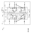
- FIG. 1A illustrates an RF-coupled digital isolator (often referred to hereafter simply as a digital isolator) 100 , according to an embodiment of the present invention.
- the digital isolator 100 includes a split leadframe 104 , including a first leadframe portion 104 a and a second leadframe portion 104 b .
- the leadframe portions 104 a and 104 b are encapsulated in an encapsulating material (e.g., plastic) to form a package 102 for the digital isolator.
- Each leadframe portion 104 a and 104 b can be made, for example, of a stamped or etched copper or steel alloy that is plated, but is not limited thereto.
- Each leadframe portion 104 a and 104 b includes a corresponding main body 110 a and 110 b and a corresponding finger 120 a and 120 b .
- the fingers 120 a and 120 b which are isolated from one another by package material (e.g., plastic molding compound), collectively provide a transformer, which may also be referred to as a “finger transformer”.
- the finger 120 a acts as a primary of the transformer
- the finger 120 b acts as a secondary of the transformer, when a radio frequency (RF) signal drives to the finger 120 a.
- RF radio frequency
- a die 130 a (also referred to as “die A”) is mounted on the main body 110 a of the leadframe portion 104 a
- a die 130 b (also referred to as “die B”) is mounted on the main body 110 b of the leadframe portion 104 b
- the die 130 a can include an integrated circuit that provides transmission capabilities, and thus may also be referred to as a transmitter die.
- the die 130 b can include an integrated circuit that provides receiving capabilities, and thus may also be referred to as a receiver die. It is also possible that each die 130 a and 130 b can provide for both transmitting and receiving capabilities, and thus may be transceiver dies. Such two way communications can be half-duplex.
- the die 130 a also includes a plurality of pads, represented by small squares within the die 130 a .
- the pads of the die 130 a are connected to components outside the die 130 a via bond wires, represented by bold lines.
- One of the pads of the die 130 a is connected to the finger 120 a by a bond wire 132 a .
- Another of the pads of the die 130 a is connected via a ground bond wire to the main body 110 a , which in turn is connected to a ground (i.e., Gnd_A) via another bond wire.
- a further pad of the die 130 a receives an input signal.
- Still another pad of the die 130 a receives a voltage (Vs_A) used to power the die 130 a.
- Vs_A voltage
- the die 130 b includes a plurality of pads, represented by small squares within the die 130 b , which are connected to components outside the die 130 b via bond wires, represented by bold lines.
- One of the pads of the die 130 b is connected to the finger 120 b by a bond wire 132 b .
- Another of the pads of the die 130 b is connected via a ground bond wire to the main body 110 b , which in turn is connected to a ground (i.e., Gnd_B) via another bond wire.
- Gnd_A and Gnd_B are electrically isolated from one another.
- a further pad of the die 130 b provides an output signal.
- Still another pad of the die 130 b receives a voltage (Vs_B) used to power the die 130 b .
- Vs_B voltage
- an RF-coupled digital isolator 100 ′ includes fingers 120 a and 120 b that are anti-parallel to one another, which causes them to be anti-phase (i.e., 180 degrees out of phase).
- a benefit of the fingers being anti-parallel to one another is that the parasitic capacitive coupling in the anti-parallel configuration increases signal transfer, due to the phrase relationships between the magnetic and coupling modes. In contrast, the parasitic capacitive coupling in the parallel configuration will reduce signal transfer.
- FIGS. 1A and 1B the fingers 120 a and 120 b are shown as being substantially straight, however that need not be the case, as can be appreciated from FIG. 1C . More specifically, FIG. 1C shows an embodiment of an RF-coupled digital isolator 100 ′′ where the fingers 120 a and 120 b are anti-parallel, but the fingers 120 a and 120 b are spiraling, which has the affect of increasing their mutual coupling inductance (and thus, increasing their coefficient of coupling).
- the fingers 120 a and 120 b in FIG. 1C can alternatively be parallel to one another. Similar or common reference numbers in the figures, including FIGS. 1A-1C , are used to reference similar components or elements.
- the distance between the fingers 120 a and 120 b , the shape of the fingers 120 a and 120 b , and the length of the fingers 120 a and 120 b affects the parasitic capacitance (C parasitic ) between the fingers and the coefficient of coupling (K).
- An exemplary distance between the fingers 120 a and 120 b is 10 milli-inches, but other distances are also within the scope of the present invention.
- the die A forces a current preferably in the GHz range into the finger 120 a , which returns into the leadframe main body 110 a and back into die A's ground bond wire.
- the fingers 120 a and 120 b which as mentioned above are isolated from one another, have a magnetic coupling and a mutual inductance.
- the parasitic capacitance is illustrated in FIG. 2 by the dashed line capacitor labeled C parasitic .
- the coefficient of coupling is illustrated by the “K” in FIG. 2 , indicating that there is a coefficient of coupling between the two fingers 120 a and 120 b (stated another way, there is a mutual inductance between the two fingers 120 a and 120 b ).
- the transfer advantageously increases with frequency. Accordingly, high operating frequencies are desired.
- the operating frequencies are preferably outside the frequency spectrums assigned to cell phones and Bluetooth devices. More specifically, it is desired that the operating frequency of the digital couplers of the present invention are greater than or less than 2.4 GHz. In specific embodiments, the operating frequency is nominally ⁇ 3 GHz.
- each of the fingers 120 a and 120 b is also shown as an inductor, also due to their inductive qualities.
- the die 130 a is also shown as including an oscillator 220 and a modulator 210 .
- the oscillator 220 produces an oscillating signal of ⁇ 3 GHz and ⁇ 3 milliamp peak-to-peak (mApp), although signals of lower or higher frequencies and/or lower or higher amplitudes are also possible and within the scope of the present invention.
- the modulator 210 receives one or more input signal lines, which instruct the modulator 210 how to control the oscillator 220 .
- simple binary modulation also known as “on/off modulation”
- the modulator 210 can be as simple as a buffer, as shown at 310 in FIG. 3 .
- Any other modulation technique that is known, or developed in the future, can alternatively be used, including, but not limited to, amplitude modulation, quadrature modulation, etc.
- the die 130 b is shown as including an RF amplifier 230 and a demodulator 240 .
- the RF amplifier 230 amplifies the signal received by the finger 120 b , and provides the amplified signal to the demodulator 240 .
- the type of demodulator used should correspond to the type of modulation provided by the modulator 210 .
- the demodulator 240 can include a rectifier 330 followed by a comparator 340 , as shown in FIG. 3 .
- FIG. 3 also illustrates that the rectifier 330 can include a diode D 1 and a capacitor C R , but is not limited thereto.
- each of the dies 130 a and 130 b optionally also includes a tuning capacitor, labeled C A and C B , used to tune the resonance of the circuit of each die.
- the parasitic capacitance (C parasitic ), mutual inductance (M), and coefficient of coupling (K) between the fingers 120 a and 120 b also affect the resonance. Accordingly, the dimensions of the fingers 120 a and 120 b , distance therebetween, and components of the circuits of each die 130 a and 130 b (including the values of tuning capacitors C A and C B ) can be selected to provide a desired resonance.
- a logic input signal provided to die A causes the oscillator 220 to oscillate and provide an RF signal to the finger transformer. More specifically, an oscillating signal is provided from the oscillator 220 , via the bond wire 132 a , to the finger 120 a .
- the oscillating current (and/or voltage) provided to the finger 120 a causes an oscillating current (and/or voltage) at the second finger 120 b , which is amplified by the amplifier 230 .
- the output of the amplifier 230 is demodulated by the demodulator 240 .
- the output of the finger transformer can recover ⁇ 45 millivolts peak-to-peak (mVpp). Presuming a Q of ⁇ 3 at each die 130 a and 130 b, ⁇ 400 mVpp can be recovered when resonating with capacitors C A and C B .
- the circuit shown in FIG. 2 can be used for one way transmission of a signal, e.g., from die A to die B, or for two way half-duplex communication.
- die A can also include an RF-amp and a demodulator
- die B can also include an oscillator and a modulator.
- a die similar to die B can also be mounted on the main body 110 a of the leadframe portion 104 a
- a die similar to die A can also be mounted on the main body 110 b of the leadframe portion 104 b .
- each lead frame portion 110 a and 110 b can include a die for transmitting signals and a separate die for receiving signals, or a common die can be for both transmitting and receiving signals.
- Each leadframe portion 104 a and 104 b need only include one finger, where half-duplex communication is used.
- the finger 120 a can be used for transmitting signals, as well as receiving signals, so long as the transmitting and receiving are occurring at different times, as is the case in half-duplex communication.
- each of the leadframe portions 104 a and 104 b can have an additional finger, as shown in FIGS. 4A and 4B .
- the leadframe portion 104 a is shown as also having a finger 420 a
- the leadframe portion 104 b is shown as also having a finger 420 b .
- the additional fingers 420 a and 420 b which are isolated from one another by package material (e.g., plastic molding compound) collectively provide a second transformer, which may also be referred to as a second “finger transformer”.
- FIGS. 4A and 4B differ from one another, in that in FIG. 4A each pair of fingers that form a finger transformer are parallel to one another, where in FIG.
- each pair of fingers that form a finger transformer are anti-parallel to one another. While the fingers in FIGS. 4A and 4B are shown as being substantially straight, that need not be the case, as can be appreciated from FIG. 1C discussed above.
- the fingers 120 a and 420 b when the fingers 120 a and 420 b are driven by RF signals, the fingers 120 a and 120 b act, respectively, as the primary and secondary of the first finger transformer, and the fingers 420 b and 420 a act, respectively, as the primary and secondary of the second finger transformer.
- the finger 120 a can be dedicated to transmitting signals and the finger 420 a can be dedicated to receiving signals, or vice versa.
- the finger 120 b can be dedicated to receiving signals, and the finger 420 b can be dedicated to transmitting signals, or vice versa. In this manner, full duplex communication can be provided.
- FIGS. 4A and 4B also show two dies 130 a and 430 a mounted on the leadframe portion 104 a , and two dies 130 b and 430 b mounted on the leadframe portion 104 b .
- One die on each leadframe portion can be used for produce signals used to drive a finger for transmission (e.g., including performing modulation), and the other die on the leadframe portion can be used, e.g., for amplifying and demodulating received signals.
- the dies shown on each leadframe portion can be combined so that each leadframe portion has mounted thereon a single die used for both receiving and transmitting functions. It is also within the scope of the present invention to add one or more additional finger(s) to each leadframe portion.
- each leadframe portion shown in FIGS. 4A and 4B can be separated into two leadframe portions, resulting in four separate leadframe portions, each having a finger.
- leadframe portions need not be symmetrical to one another, i.e., non-symmetrical layouts can also be used.
- the digital isolator can be formed in a ceramic package, such as but not limited to a hermetic ceramic package.
- a ceramic package can include a lead frame embedded in a paste layer between ceramic top and bottom covers.
- the leadframe portions 104 a and 104 b that include a corresponding finger 120 and main body 110 can be embedded between ceramic layers.
- the dies e.g., 130 a and 130 b
- air or some other gas can provide electrical isolation between a pair of fingers.
- the main bodies (e.g., 110 a and 110 b ) and fingers (e.g., 120 a and 120 b ) be formed directly on a ceramic layer using any of a variety of techniques, such as, but not limited to, chemical vapor deposition, sputtering, etching, photolithography, masking, etc.
- the dies (e.g., 130 a and 130 b ) can be connected to such a layer, which may or may not be the same layer on which the fingers 120 are formed. Again, air or some other gas can provide electrical isolation between a pair of fingers.
- the digital isolator can be formed as a hybrid integrated circuit.
- the main bodies (e.g., 110 a and 110 b ) and fingers (e.g., 120 a and 120 b ) can be formed on a printed circuit board, to which are attached the dies (e.g., 130 a and 130 b ).
- the dies e.g., 130 a and 130 b
- molding compound can provide electrical isolation and mechanical support between fingers.
- conductive traces and/or vias can be used in place of bond wires to connect dies to fingers, or bond wires can still be used.
- An advantage of certain embodiments of the present invention is that a digital isolator can be provided by producing a transformer using a split leadframe and plastic molding compound that are available in typically chip assembly processes.
- An advantage of certain embodiments of the present invention is that no windings are necessary to provide a transformer for a digital isolator, likely reducing the size and cost of a resulting digital isolator.
- Another advantage of certain embodiments of the present invention is that the designs discussed above work well at high frequencies above cell phone and Bluetooth spectrums, and such embodiments, if tuned appropriately, can also inherently reject frequencies in the cell phone and Bluetooth spectrums.
- the RF-coupled digital isolators of the present invention can be used for numerous different applications.
- the RF-coupled digital isolators can be used in a power H-bridge, e.g., in power supplies or motor controllers, e.g., as shown in FIG. 5 .
- Other implementation of an H-bridge are also possible, and within the scope of the present invention.
- the RF-coupled digital isolators can be used to communicate with switching power transistors and power lines. Further, the RF-coupled digital isolators of the present invention can be used for long distance communications (e.g., RS485). The RF-coupled digital isolators of the present invention can be especially useful for power switching of 50 W or greater. The RF-coupled digital isolators of the present invention can also be used to reduce dead time for DC to DC converters, e.g., to 10 nsec. These are just a few applications for the digital isolators of the present invention, which are not meant to be limiting.
Abstract
Description
Claims (21)
Priority Applications (5)
| Application Number | Priority Date | Filing Date | Title |
|---|---|---|---|
| US11/877,333 US7468547B2 (en) | 2007-05-11 | 2007-10-23 | RF-coupled digital isolator |
| CN200880015420XA CN101681901B (en) | 2007-05-11 | 2008-03-21 | RF-coupled digital isolator |
| PCT/US2008/057909 WO2008140861A1 (en) | 2007-05-11 | 2008-03-21 | Rf - coupled digital isolator |
| TW097112605A TWI460919B (en) | 2007-05-11 | 2008-04-08 | Rf-coupled digital isolator |
| US12/163,256 US8080865B2 (en) | 2007-05-11 | 2008-06-27 | RF-coupled digital isolator |
Applications Claiming Priority (3)
| Application Number | Priority Date | Filing Date | Title |
|---|---|---|---|
| US92885607P | 2007-05-11 | 2007-05-11 | |
| US97302007P | 2007-09-17 | 2007-09-17 | |
| US11/877,333 US7468547B2 (en) | 2007-05-11 | 2007-10-23 | RF-coupled digital isolator |
Related Child Applications (1)
| Application Number | Title | Priority Date | Filing Date |
|---|---|---|---|
| US12/163,256 Continuation US8080865B2 (en) | 2007-05-11 | 2008-06-27 | RF-coupled digital isolator |
Publications (2)
| Publication Number | Publication Date |
|---|---|
| US20080278255A1 US20080278255A1 (en) | 2008-11-13 |
| US7468547B2 true US7468547B2 (en) | 2008-12-23 |
Family
ID=39968982
Family Applications (2)
| Application Number | Title | Priority Date | Filing Date |
|---|---|---|---|
| US11/877,333 Expired - Fee Related US7468547B2 (en) | 2007-05-11 | 2007-10-23 | RF-coupled digital isolator |
| US12/163,256 Expired - Fee Related US8080865B2 (en) | 2007-05-11 | 2008-06-27 | RF-coupled digital isolator |
Family Applications After (1)
| Application Number | Title | Priority Date | Filing Date |
|---|---|---|---|
| US12/163,256 Expired - Fee Related US8080865B2 (en) | 2007-05-11 | 2008-06-27 | RF-coupled digital isolator |
Country Status (4)
| Country | Link |
|---|---|
| US (2) | US7468547B2 (en) |
| CN (1) | CN101681901B (en) |
| TW (1) | TWI460919B (en) |
| WO (1) | WO2008140861A1 (en) |
Cited By (29)
| Publication number | Priority date | Publication date | Assignee | Title |
|---|---|---|---|---|
| US8093983B2 (en) * | 2006-08-28 | 2012-01-10 | Avago Technologies Ecbu Ip (Singapore) Pte. Ltd. | Narrowbody coil isolator |
| US8772909B1 (en) | 2012-10-04 | 2014-07-08 | Vlt, Inc. | Isolator with integral transformer |
| US20140203870A1 (en) * | 2007-04-13 | 2014-07-24 | Advanced Analogic Technologies Incorporated | Power mosfets with improved efficiency for multi-channel class d audio amplifiers and packaging therefor |
| US8976561B2 (en) | 2012-11-14 | 2015-03-10 | Power Integrations, Inc. | Switch mode power converters using magnetically coupled galvanically isolated lead frame communication |
| US9019728B2 (en) | 2013-03-08 | 2015-04-28 | Power Integrations, Inc. | Power converter output voltage clamp and supply terminal |
| US9035435B2 (en) | 2012-11-14 | 2015-05-19 | Power Integrations, Inc. | Magnetically coupled galvanically isolated communication using lead frame |
| US9071146B2 (en) | 2013-03-13 | 2015-06-30 | Power Integrations, Inc. | AC voltage sensor with low power consumption |
| US9087713B2 (en) | 2012-10-12 | 2015-07-21 | Power Integrations, Inc. | Semiconductor device with shared region |
| US9136765B2 (en) | 2013-03-08 | 2015-09-15 | Power Integrations, Inc. | Techniques for controlling a power converter using multiple controllers |
| US9166486B2 (en) | 2013-03-08 | 2015-10-20 | Power Integrations, Inc. | Power converter using multiple controllers |
| US9166575B2 (en) | 2013-03-08 | 2015-10-20 | Power Integrations, Inc. | Low threshold voltage comparator |
| US9178411B2 (en) | 2013-01-22 | 2015-11-03 | Power Integrations, Inc. | Charging circuit for a power converter controller |
| US9246392B2 (en) | 2013-03-13 | 2016-01-26 | Power Integrations, Inc. | Switched mode power converter controller with ramp time modulation |
| US9261538B2 (en) | 2014-06-06 | 2016-02-16 | Solantro Semiconductor Corp. | Isolating interchip communication circuit and method |
| US9276479B2 (en) | 2013-01-22 | 2016-03-01 | Power Integrations, Inc. | Receive circuit for use in a power converter |
| US9331587B2 (en) | 2013-01-22 | 2016-05-03 | Power Integrations, Inc. | Power converter controller with multiple power sources |
| US9349717B2 (en) | 2012-11-14 | 2016-05-24 | Power Integrations, Inc. | Noise cancellation for a magnetically coupled communication link utilizing a lead frame |
| US9374011B2 (en) | 2013-01-22 | 2016-06-21 | Power Integrations, Inc. | Secondary controller for use in synchronous flyback converter |
| US9401657B2 (en) | 2013-03-13 | 2016-07-26 | Power Integrations, Inc. | Input voltage sensor responsive to load conditions |
| US9496926B2 (en) | 2013-05-24 | 2016-11-15 | Texas Instruments Incorporated | Galvanic isolator |
| US9508485B1 (en) | 2012-10-04 | 2016-11-29 | Vlt, Inc. | Isolator with integral transformer |
| US9704639B2 (en) | 2014-11-07 | 2017-07-11 | Solantro Semiconductor Corp. | Non-planar inductive electrical elements in semiconductor package lead frame |
| US9967984B1 (en) | 2015-01-14 | 2018-05-08 | Vlt, Inc. | Power adapter packaging |
| US10243442B1 (en) | 2017-11-22 | 2019-03-26 | Power Integrations, Inc. | Controller with frequency to on-time converter |
| US10264664B1 (en) | 2015-06-04 | 2019-04-16 | Vlt, Inc. | Method of electrically interconnecting circuit assemblies |
| US10805123B2 (en) | 2018-03-07 | 2020-10-13 | Texas Instruments Incorporated | Crosstalk generation and detection for digital isolators |
| US10854538B2 (en) | 2019-02-12 | 2020-12-01 | Texas Instruments Incorporated | Microelectronic device with floating pads |
| US11240070B1 (en) * | 2020-10-30 | 2022-02-01 | Feature Integration Technology Inc. | Digital isolator |
| US11706057B2 (en) | 2021-06-18 | 2023-07-18 | Nunami Inc. | Devices, systems, and methods for serial communication over a galvanically isolated channel |
Families Citing this family (26)
| Publication number | Priority date | Publication date | Assignee | Title |
|---|---|---|---|---|
| US8198951B2 (en) * | 2004-06-03 | 2012-06-12 | Silicon Laboratories Inc. | Capacitive isolation circuitry |
| US8427844B2 (en) | 2006-08-28 | 2013-04-23 | Avago Technologies Ecbu Ip (Singapore) Pte. Ltd. | Widebody coil isolators |
| US9105391B2 (en) | 2006-08-28 | 2015-08-11 | Avago Technologies General Ip (Singapore) Pte. Ltd. | High voltage hold-off coil transducer |
| US9019057B2 (en) | 2006-08-28 | 2015-04-28 | Avago Technologies General Ip (Singapore) Pte. Ltd. | Galvanic isolators and coil transducers |
| US7564292B2 (en) * | 2007-09-28 | 2009-07-21 | Alpha & Omega Semiconductor, Inc. | Device and method for limiting Di/Dt caused by a switching FET of an inductive switching circuit |
| US9723766B2 (en) * | 2010-09-10 | 2017-08-01 | Intersil Americas LLC | Power supply module with electromagnetic-interference (EMI) shielding, cooling, or both shielding and cooling, along two or more sides |
| US9143366B2 (en) | 2012-09-07 | 2015-09-22 | The Aerospace Corporation | Galvanic isolation interface for high-speed data link for spacecraft electronics, and method of using same |
| US9698728B2 (en) | 2012-12-13 | 2017-07-04 | Texas Instruments Incorporated | Digital isolator |
| US10840005B2 (en) | 2013-01-25 | 2020-11-17 | Vishay Dale Electronics, Llc | Low profile high current composite transformer |
| US10536309B2 (en) | 2014-09-15 | 2020-01-14 | Analog Devices, Inc. | Demodulation of on-off-key modulated signals in signal isolator systems |
| US10270630B2 (en) | 2014-09-15 | 2019-04-23 | Analog Devices, Inc. | Demodulation of on-off-key modulated signals in signal isolator systems |
| US9660848B2 (en) * | 2014-09-15 | 2017-05-23 | Analog Devices Global | Methods and structures to generate on/off keyed carrier signals for signal isolators |
| US9998301B2 (en) | 2014-11-03 | 2018-06-12 | Analog Devices, Inc. | Signal isolator system with protection for common mode transients |
| WO2016196189A1 (en) | 2015-05-31 | 2016-12-08 | Skyworks Solutions, Inc. | Shielded module having compression overmold |
| US10998124B2 (en) | 2016-05-06 | 2021-05-04 | Vishay Dale Electronics, Llc | Nested flat wound coils forming windings for transformers and inductors |
| US10205442B2 (en) * | 2016-08-08 | 2019-02-12 | Analog Devices Global | Galvanically isolated data isolator with improved common mode transient rejection |
| WO2018045007A1 (en) | 2016-08-31 | 2018-03-08 | Vishay Dale Electronics, Llc | Inductor having high current coil with low direct current resistance |
| CN106816295B (en) * | 2016-12-27 | 2019-04-26 | 德清崎辉机械科技有限公司 | A kind of external hanging type integrated-type small-power medical isolating transformer device |
| US9893759B1 (en) | 2017-04-25 | 2018-02-13 | Sprint Communications Company L.P. | Wireless relay antenna isolation |
| CN109712793B (en) * | 2017-10-25 | 2020-10-30 | 光宝科技新加坡私人有限公司 | Turnover type magnetic coupling packaging structure and lead frame assembly and manufacturing method thereof |
| US10345832B1 (en) * | 2018-05-14 | 2019-07-09 | Asm Ip Holding B.V. | Insulation system and substrate processing apparatus |
| US11329025B2 (en) * | 2020-03-24 | 2022-05-10 | Texas Instruments Incorporated | Multi-chip package with reinforced isolation |
| JP2021153239A (en) * | 2020-03-24 | 2021-09-30 | 株式会社東芝 | Isolator |
| US11205611B1 (en) * | 2020-06-15 | 2021-12-21 | Texas Instruments Incorporated | Leadframe capacitors |
| US11948724B2 (en) | 2021-06-18 | 2024-04-02 | Vishay Dale Electronics, Llc | Method for making a multi-thickness electro-magnetic device |
| US11711894B1 (en) | 2022-02-03 | 2023-07-25 | Analog Devices International Unlimited Company | Capacitively coupled resonators for high frequency galvanic isolators |
Citations (8)
| Publication number | Priority date | Publication date | Assignee | Title |
|---|---|---|---|---|
| US5162970A (en) | 1992-01-27 | 1992-11-10 | American Technical Ceramics Corporation | Miniature monolithic ceramic coupler for electronic circuits |
| US5428245A (en) * | 1994-05-06 | 1995-06-27 | National Semiconductor Corporation | Lead frame including an inductor or other such magnetic component |
| US5444600A (en) * | 1992-12-03 | 1995-08-22 | Linear Technology Corporation | Lead frame capacitor and capacitively-coupled isolator circuit using the same |
| JPH09260569A (en) | 1996-03-25 | 1997-10-03 | Toshiba Corp | Resin sealed semiconductor device |
| US6621140B1 (en) * | 2002-02-25 | 2003-09-16 | Rf Micro Devices, Inc. | Leadframe inductors |
| US20050271148A1 (en) | 2004-06-03 | 2005-12-08 | Timothy Dupuis | RF isolator with differential input/output |
| US7064442B1 (en) * | 2003-07-02 | 2006-06-20 | Analog Devices, Inc. | Integrated circuit package device |
| US20060214271A1 (en) * | 2005-03-23 | 2006-09-28 | Jeremy Loraine | Device and applications for passive RF components in leadframes |
Family Cites Families (7)
| Publication number | Priority date | Publication date | Assignee | Title |
|---|---|---|---|---|
| US7902627B2 (en) * | 2004-06-03 | 2011-03-08 | Silicon Laboratories Inc. | Capacitive isolation circuitry with improved common mode detector |
| US8441325B2 (en) * | 2004-06-03 | 2013-05-14 | Silicon Laboratories Inc. | Isolator with complementary configurable memory |
| FI20055402A0 (en) * | 2005-07-11 | 2005-07-11 | Nokia Corp | Inductor for multi-band radio frequency operation |
| US20070096269A1 (en) * | 2005-10-31 | 2007-05-03 | Mediatek Inc. | Leadframe for semiconductor packages |
| US7852186B2 (en) * | 2006-08-28 | 2010-12-14 | Avago Technologies Ecbu Ip (Singapore) Pte. Ltd. | Coil transducer with reduced arcing and improved high voltage breakdown performance characteristics |
| US7791900B2 (en) * | 2006-08-28 | 2010-09-07 | Avago Technologies General Ip (Singapore) Pte. Ltd. | Galvanic isolator |
| US8477856B2 (en) * | 2009-03-31 | 2013-07-02 | Analog Devices, Inc. | Multi-bit digital signal isolator |
-
2007
- 2007-10-23 US US11/877,333 patent/US7468547B2/en not_active Expired - Fee Related
-
2008
- 2008-03-21 WO PCT/US2008/057909 patent/WO2008140861A1/en active Application Filing
- 2008-03-21 CN CN200880015420XA patent/CN101681901B/en not_active Expired - Fee Related
- 2008-04-08 TW TW097112605A patent/TWI460919B/en not_active IP Right Cessation
- 2008-06-27 US US12/163,256 patent/US8080865B2/en not_active Expired - Fee Related
Patent Citations (13)
| Publication number | Priority date | Publication date | Assignee | Title |
|---|---|---|---|---|
| US5162970A (en) | 1992-01-27 | 1992-11-10 | American Technical Ceramics Corporation | Miniature monolithic ceramic coupler for electronic circuits |
| US5926358A (en) * | 1992-12-03 | 1999-07-20 | Linear Technology Corporation | Lead frame capacitor and capacitively-coupled isolator circuit using same |
| US5444600A (en) * | 1992-12-03 | 1995-08-22 | Linear Technology Corporation | Lead frame capacitor and capacitively-coupled isolator circuit using the same |
| US5589709A (en) * | 1992-12-03 | 1996-12-31 | Linear Technology Inc. | Lead frame capacitor and capacitively-coupled isolator circuit using same |
| US5650357A (en) * | 1992-12-03 | 1997-07-22 | Linear Technology Corporation | Process for manufacturing a lead frame capacitor and capacitively-coupled isolator circuit using same |
| US5945728A (en) * | 1992-12-03 | 1999-08-31 | Linear Technology Corporation | Lead frame capacitor and capacitively coupled isolator circuit |
| US5428245A (en) * | 1994-05-06 | 1995-06-27 | National Semiconductor Corporation | Lead frame including an inductor or other such magnetic component |
| JPH09260569A (en) | 1996-03-25 | 1997-10-03 | Toshiba Corp | Resin sealed semiconductor device |
| US6621140B1 (en) * | 2002-02-25 | 2003-09-16 | Rf Micro Devices, Inc. | Leadframe inductors |
| US20040214376A1 (en) | 2002-02-25 | 2004-10-28 | Nortel Networks Limited | Leadframe inductors |
| US7064442B1 (en) * | 2003-07-02 | 2006-06-20 | Analog Devices, Inc. | Integrated circuit package device |
| US20050271148A1 (en) | 2004-06-03 | 2005-12-08 | Timothy Dupuis | RF isolator with differential input/output |
| US20060214271A1 (en) * | 2005-03-23 | 2006-09-28 | Jeremy Loraine | Device and applications for passive RF components in leadframes |
Non-Patent Citations (5)
| Title |
|---|
| "3.3-V/5-V High Speed Isolators," ISO721, ISO721M, ISO722, ISO722M, Texas Instruments Incorporated (revised Feb. 2007), http://focus.ti.com/lit/ds/slls629d/slls629d.pdf. |
| "Digital Isolators," Silicon Laboratories, Inc. (2007), http://www.silabs.com/tgwWebApp/public/web-content/products/Digital-Power/Isolators/en/Si844x.htm. |
| "Dual Digital Isolator," IL711/712, NVE Corporation (Oct. 2002), http://home.nve.com/Downloads/il711-2t.pdf. |
| "Triple Channel Digital Isolators," ADuM1300/ADuM1301, Analog Devices (2003-2007), http://www.analog.com/UploadedFiles/Data-Sheets/ADUM1300-1301.pdf. |
| International Search Report and Written Opinion for PCT/US2008/057909. |
Cited By (54)
| Publication number | Priority date | Publication date | Assignee | Title |
|---|---|---|---|---|
| US8093983B2 (en) * | 2006-08-28 | 2012-01-10 | Avago Technologies Ecbu Ip (Singapore) Pte. Ltd. | Narrowbody coil isolator |
| US20140203870A1 (en) * | 2007-04-13 | 2014-07-24 | Advanced Analogic Technologies Incorporated | Power mosfets with improved efficiency for multi-channel class d audio amplifiers and packaging therefor |
| US9246449B2 (en) * | 2007-04-13 | 2016-01-26 | Advanced Analogic Technologies Incorporated | Power MOSFETs with improved efficiency for multi-channel class D audio amplifiers and packaging therefor |
| US8772909B1 (en) | 2012-10-04 | 2014-07-08 | Vlt, Inc. | Isolator with integral transformer |
| US9508485B1 (en) | 2012-10-04 | 2016-11-29 | Vlt, Inc. | Isolator with integral transformer |
| US9087713B2 (en) | 2012-10-12 | 2015-07-21 | Power Integrations, Inc. | Semiconductor device with shared region |
| US9831188B2 (en) | 2012-11-14 | 2017-11-28 | Power Integrations, Inc. | Noise cancellation for a magnetically coupled communication link utilizing a lead frame |
| US9275946B2 (en) | 2012-11-14 | 2016-03-01 | Power Integrations, Inc. | Switch mode power converters using magnetically coupled galvanically isolated lead frame communication |
| US9035435B2 (en) | 2012-11-14 | 2015-05-19 | Power Integrations, Inc. | Magnetically coupled galvanically isolated communication using lead frame |
| US10361632B2 (en) | 2012-11-14 | 2019-07-23 | Power Integrations, Inc. | Magnetically coupled galvanically isolated communication using lead frame |
| US10079543B2 (en) | 2012-11-14 | 2018-09-18 | Power Intergrations, Inc. | Magnetically coupled galvanically isolated communication using lead frame |
| US9349717B2 (en) | 2012-11-14 | 2016-05-24 | Power Integrations, Inc. | Noise cancellation for a magnetically coupled communication link utilizing a lead frame |
| US10224292B2 (en) | 2012-11-14 | 2019-03-05 | Power Integrations, Inc. | Noise cancellation for a magnetically coupled communication link utilizing a lead frame |
| US8976561B2 (en) | 2012-11-14 | 2015-03-10 | Power Integrations, Inc. | Switch mode power converters using magnetically coupled galvanically isolated lead frame communication |
| US9331004B2 (en) | 2012-11-14 | 2016-05-03 | Power Integrations, Inc. | Magnetically coupled galvanically isolated communication using lead frame |
| US11088621B2 (en) | 2013-01-22 | 2021-08-10 | Power Integrations, Inc. | Secondary controller for use in synchronous flyback converter |
| US10243471B2 (en) | 2013-01-22 | 2019-03-26 | Power Integrations, Inc. | Power converter controller with multiple power sources |
| US9331587B2 (en) | 2013-01-22 | 2016-05-03 | Power Integrations, Inc. | Power converter controller with multiple power sources |
| US11824453B2 (en) | 2013-01-22 | 2023-11-21 | Power Integrations, Inc. | Secondary controller for use in synchronous flyback converter |
| US9178411B2 (en) | 2013-01-22 | 2015-11-03 | Power Integrations, Inc. | Charging circuit for a power converter controller |
| US9374011B2 (en) | 2013-01-22 | 2016-06-21 | Power Integrations, Inc. | Secondary controller for use in synchronous flyback converter |
| US9276479B2 (en) | 2013-01-22 | 2016-03-01 | Power Integrations, Inc. | Receive circuit for use in a power converter |
| US9166486B2 (en) | 2013-03-08 | 2015-10-20 | Power Integrations, Inc. | Power converter using multiple controllers |
| US9136765B2 (en) | 2013-03-08 | 2015-09-15 | Power Integrations, Inc. | Techniques for controlling a power converter using multiple controllers |
| US9627985B2 (en) | 2013-03-08 | 2017-04-18 | Power Integrations, Inc. | Power converter output voltage clamp and supply terminal |
| US9166575B2 (en) | 2013-03-08 | 2015-10-20 | Power Integrations, Inc. | Low threshold voltage comparator |
| US9762129B2 (en) | 2013-03-08 | 2017-09-12 | Power Integrations, Inc. | Techniques for controlling a power converter using multiple controllers |
| US11309800B2 (en) | 2013-03-08 | 2022-04-19 | Power Integrations, Inc. | Techniques for controlling a power converter using multiple controllers |
| US10230305B2 (en) | 2013-03-08 | 2019-03-12 | Power Integrations, Inc. | Techniques for controlling a power converter using multiple controllers |
| US9019728B2 (en) | 2013-03-08 | 2015-04-28 | Power Integrations, Inc. | Power converter output voltage clamp and supply terminal |
| US9929656B2 (en) | 2013-03-08 | 2018-03-27 | Power Integrations, Inc. | Power converter using multiple controllers |
| US9246392B2 (en) | 2013-03-13 | 2016-01-26 | Power Integrations, Inc. | Switched mode power converter controller with ramp time modulation |
| US10158295B2 (en) | 2013-03-13 | 2018-12-18 | Power Integrations, Inc. | Switched mode power converter controller with ramp time modulation |
| US9866125B2 (en) | 2013-03-13 | 2018-01-09 | Power Integrations, Inc. | Input voltage sensor responsive to load conditions |
| US9837911B2 (en) | 2013-03-13 | 2017-12-05 | Power Integrations, Inc. | Switched mode power converter controller with ramp time modulation |
| US9401657B2 (en) | 2013-03-13 | 2016-07-26 | Power Integrations, Inc. | Input voltage sensor responsive to load conditions |
| US11349398B2 (en) | 2013-03-13 | 2022-05-31 | Power Integrations, Inc | Switched mode power converter controller with ramp time modulation |
| US10811977B2 (en) | 2013-03-13 | 2020-10-20 | Power Integrations, Inc. | Switched mode power converter controller with ramp time modulation |
| US9071146B2 (en) | 2013-03-13 | 2015-06-30 | Power Integrations, Inc. | AC voltage sensor with low power consumption |
| US10594162B2 (en) | 2013-05-24 | 2020-03-17 | Texas Instruments Incorporated | Galvanic isolator |
| US9496926B2 (en) | 2013-05-24 | 2016-11-15 | Texas Instruments Incorporated | Galvanic isolator |
| US9261538B2 (en) | 2014-06-06 | 2016-02-16 | Solantro Semiconductor Corp. | Isolating interchip communication circuit and method |
| US9704639B2 (en) | 2014-11-07 | 2017-07-11 | Solantro Semiconductor Corp. | Non-planar inductive electrical elements in semiconductor package lead frame |
| US10398040B1 (en) | 2015-01-14 | 2019-08-27 | Vlt, Inc. | Power adapter packaging |
| US9967984B1 (en) | 2015-01-14 | 2018-05-08 | Vlt, Inc. | Power adapter packaging |
| US10537015B1 (en) | 2015-06-04 | 2020-01-14 | Vlt, Inc. | Methods of forming modular assemblies |
| US10264664B1 (en) | 2015-06-04 | 2019-04-16 | Vlt, Inc. | Method of electrically interconnecting circuit assemblies |
| US11324107B1 (en) | 2015-06-04 | 2022-05-03 | Vicor Corporation | Panel molded electronic assemblies with multi-surface conductive contacts |
| US10243442B1 (en) | 2017-11-22 | 2019-03-26 | Power Integrations, Inc. | Controller with frequency to on-time converter |
| US10805123B2 (en) | 2018-03-07 | 2020-10-13 | Texas Instruments Incorporated | Crosstalk generation and detection for digital isolators |
| US10854538B2 (en) | 2019-02-12 | 2020-12-01 | Texas Instruments Incorporated | Microelectronic device with floating pads |
| US11538743B2 (en) | 2019-02-12 | 2022-12-27 | Texas Instruments Incorporated | Microelectronic device with floating pads |
| US11240070B1 (en) * | 2020-10-30 | 2022-02-01 | Feature Integration Technology Inc. | Digital isolator |
| US11706057B2 (en) | 2021-06-18 | 2023-07-18 | Nunami Inc. | Devices, systems, and methods for serial communication over a galvanically isolated channel |
Also Published As
| Publication number | Publication date |
|---|---|
| US8080865B2 (en) | 2011-12-20 |
| TWI460919B (en) | 2014-11-11 |
| US20080278255A1 (en) | 2008-11-13 |
| US20080278256A1 (en) | 2008-11-13 |
| CN101681901A (en) | 2010-03-24 |
| CN101681901B (en) | 2011-07-27 |
| WO2008140861A1 (en) | 2008-11-20 |
| TW200901551A (en) | 2009-01-01 |
Similar Documents
| Publication | Publication Date | Title |
|---|---|---|
| US7468547B2 (en) | RF-coupled digital isolator | |
| US10447230B2 (en) | Transformer of the balanced-unbalanced type | |
| US7683733B2 (en) | Balun transformer with improved harmonic suppression | |
| KR101119910B1 (en) | Mobile RFID Reader Transceiver System | |
| US8592944B2 (en) | Semiconductor electronic device with an integrated device with an integrated galvanic isolator element and related assembly process | |
| US9991721B2 (en) | System and method for inductive wireless signaling | |
| US6462620B1 (en) | RF power amplifier circuitry and method for amplifying signals | |
| US9761545B2 (en) | Isolator and method of manufacturing isolator | |
| US10997483B2 (en) | NFC antenna switch | |
| US6392488B1 (en) | Dual oxide gate device and method for providing the same | |
| US20050271148A1 (en) | RF isolator with differential input/output | |
| US9224534B2 (en) | Electromagnetic resonance coupler | |
| JP4592542B2 (en) | Semiconductor device | |
| EP1045442A2 (en) | Semiconductor integrated circuit | |
| KR101631364B1 (en) | Methods and devices for semiconductor chip configuration with a coupler | |
| US6362606B1 (en) | Method and apparatus for regulating a voltage | |
| JP4098562B2 (en) | Method and semiconductor structure to reduce energy loss in resonant circuit of passive transponder | |
| Javid et al. | A 650 kV/μs common-mode resilient CMOS galvanically isolated communication system | |
| US20090096532A1 (en) | Differential amplifier with single ended output | |
| CN109951210B (en) | Monolithic integrated full-isolation RS-232 transceiver | |
| US11621670B1 (en) | Capacitively-coupled stacked class-d oscillators for galvanic isolation | |
| TW201438413A (en) | Isolation communication technology using coupled oscillators/antennas | |
| US20220093581A1 (en) | Ic package providing isolated filter on lead-frame | |
| JP2006032805A (en) | Voltage control oscillation circuit and semiconductor integrated device and wireless communication device using the circuit | |
| US8373210B2 (en) | Semiconductor device and semiconductor device manufacturing method |
Legal Events
| Date | Code | Title | Description |
|---|---|---|---|
| AS | Assignment |
Owner name: INTERSIL AMERICAS INC., CALIFORNIA Free format text: ASSIGNMENT OF ASSIGNORS INTEREST;ASSIGNOR:HARVEY, BARRY;REEL/FRAME:020002/0856 Effective date: 20071022 |
|
| STCF | Information on status: patent grant |
Free format text: PATENTED CASE |
|
| AS | Assignment |
Owner name: MORGAN STANLEY & CO. INCORPORATED,NEW YORK Free format text: SECURITY AGREEMENT;ASSIGNORS:INTERSIL CORPORATION;TECHWELL, INC.;INTERSIL COMMUNICATIONS, INC.;AND OTHERS;REEL/FRAME:024329/0411 Effective date: 20100427 Owner name: MORGAN STANLEY & CO. INCORPORATED, NEW YORK Free format text: SECURITY AGREEMENT;ASSIGNORS:INTERSIL CORPORATION;TECHWELL, INC.;INTERSIL COMMUNICATIONS, INC.;AND OTHERS;REEL/FRAME:024329/0411 Effective date: 20100427 |
|
| FPAY | Fee payment |
Year of fee payment: 4 |
|
| AS | Assignment |
Owner name: INTERSIL AMERICAS LLC, CALIFORNIA Free format text: CHANGE OF NAME;ASSIGNOR:INTERSIL AMERICAS INC.;REEL/FRAME:033119/0484 Effective date: 20111223 |
|
| FPAY | Fee payment |
Year of fee payment: 8 |
|
| FEPP | Fee payment procedure |
Free format text: MAINTENANCE FEE REMINDER MAILED (ORIGINAL EVENT CODE: REM.); ENTITY STATUS OF PATENT OWNER: LARGE ENTITY |
|
| LAPS | Lapse for failure to pay maintenance fees |
Free format text: PATENT EXPIRED FOR FAILURE TO PAY MAINTENANCE FEES (ORIGINAL EVENT CODE: EXP.); ENTITY STATUS OF PATENT OWNER: LARGE ENTITY |
|
| STCH | Information on status: patent discontinuation |
Free format text: PATENT EXPIRED DUE TO NONPAYMENT OF MAINTENANCE FEES UNDER 37 CFR 1.362 |
|
| FP | Lapsed due to failure to pay maintenance fee |
Effective date: 20201223 |