US7511331B2 - Semiconductor device having side wall spacers - Google Patents
Semiconductor device having side wall spacers Download PDFInfo
- Publication number
- US7511331B2 US7511331B2 US12/007,420 US742008A US7511331B2 US 7511331 B2 US7511331 B2 US 7511331B2 US 742008 A US742008 A US 742008A US 7511331 B2 US7511331 B2 US 7511331B2
- Authority
- US
- United States
- Prior art keywords
- film
- side wall
- gate electrode
- oxide film
- semiconductor substrate
- Prior art date
- Legal status (The legal status is an assumption and is not a legal conclusion. Google has not performed a legal analysis and makes no representation as to the accuracy of the status listed.)
- Expired - Fee Related
Links
- 239000004065 semiconductor Substances 0.000 title claims abstract description 92
- 125000006850 spacer group Chemical group 0.000 title claims abstract description 84
- 239000000758 substrate Substances 0.000 claims abstract description 86
- 150000004767 nitrides Chemical class 0.000 claims abstract description 17
- 229910052581 Si3N4 Inorganic materials 0.000 claims description 56
- HQVNEWCFYHHQES-UHFFFAOYSA-N silicon nitride Chemical compound N12[Si]34N5[Si]62N3[Si]51N64 HQVNEWCFYHHQES-UHFFFAOYSA-N 0.000 claims description 56
- 230000005641 tunneling Effects 0.000 claims description 15
- 230000004888 barrier function Effects 0.000 abstract description 10
- VYPSYNLAJGMNEJ-UHFFFAOYSA-N Silicium dioxide Chemical compound O=[Si]=O VYPSYNLAJGMNEJ-UHFFFAOYSA-N 0.000 description 60
- 229910052814 silicon oxide Inorganic materials 0.000 description 60
- 238000005530 etching Methods 0.000 description 55
- 239000010410 layer Substances 0.000 description 45
- 238000000034 method Methods 0.000 description 38
- XUIMIQQOPSSXEZ-UHFFFAOYSA-N Silicon Chemical compound [Si] XUIMIQQOPSSXEZ-UHFFFAOYSA-N 0.000 description 26
- 229910052710 silicon Inorganic materials 0.000 description 26
- 239000010703 silicon Substances 0.000 description 26
- KRHYYFGTRYWZRS-UHFFFAOYSA-N Fluorane Chemical compound F KRHYYFGTRYWZRS-UHFFFAOYSA-N 0.000 description 22
- 238000004519 manufacturing process Methods 0.000 description 19
- 230000008569 process Effects 0.000 description 18
- 229910021420 polycrystalline silicon Inorganic materials 0.000 description 16
- 229920005591 polysilicon Polymers 0.000 description 16
- 229910021332 silicide Inorganic materials 0.000 description 16
- FVBUAEGBCNSCDD-UHFFFAOYSA-N silicide(4-) Chemical compound [Si-4] FVBUAEGBCNSCDD-UHFFFAOYSA-N 0.000 description 16
- BOTDANWDWHJENH-UHFFFAOYSA-N Tetraethyl orthosilicate Chemical compound CCO[Si](OCC)(OCC)OCC BOTDANWDWHJENH-UHFFFAOYSA-N 0.000 description 15
- 150000002500 ions Chemical class 0.000 description 12
- 239000000243 solution Substances 0.000 description 12
- 238000002955 isolation Methods 0.000 description 11
- 239000002184 metal Substances 0.000 description 11
- 229910052751 metal Inorganic materials 0.000 description 11
- 230000003647 oxidation Effects 0.000 description 11
- 238000007254 oxidation reaction Methods 0.000 description 11
- 238000005229 chemical vapour deposition Methods 0.000 description 10
- 229910021417 amorphous silicon Inorganic materials 0.000 description 9
- 239000011229 interlayer Substances 0.000 description 9
- 239000012535 impurity Substances 0.000 description 8
- 238000006243 chemical reaction Methods 0.000 description 7
- 238000005468 ion implantation Methods 0.000 description 6
- 238000001020 plasma etching Methods 0.000 description 6
- XPDWGBQVDMORPB-UHFFFAOYSA-N Fluoroform Chemical compound FC(F)F XPDWGBQVDMORPB-UHFFFAOYSA-N 0.000 description 5
- 238000003475 lamination Methods 0.000 description 5
- 238000009792 diffusion process Methods 0.000 description 4
- 238000004544 sputter deposition Methods 0.000 description 4
- ATJFFYVFTNAWJD-UHFFFAOYSA-N Tin Chemical compound [Sn] ATJFFYVFTNAWJD-UHFFFAOYSA-N 0.000 description 3
- 230000001133 acceleration Effects 0.000 description 3
- 238000010586 diagram Methods 0.000 description 3
- 230000006870 function Effects 0.000 description 3
- 238000010438 heat treatment Methods 0.000 description 3
- 238000004151 rapid thermal annealing Methods 0.000 description 3
- 239000002344 surface layer Substances 0.000 description 3
- 238000000137 annealing Methods 0.000 description 2
- 238000000151 deposition Methods 0.000 description 2
- 230000014759 maintenance of location Effects 0.000 description 2
- 239000000203 mixture Substances 0.000 description 2
- 230000002093 peripheral effect Effects 0.000 description 2
- 229920002120 photoresistant polymer Polymers 0.000 description 2
- 238000005268 plasma chemical vapour deposition Methods 0.000 description 2
- 230000005689 Fowler Nordheim tunneling Effects 0.000 description 1
- 239000002131 composite material Substances 0.000 description 1
- 230000003111 delayed effect Effects 0.000 description 1
- 238000001312 dry etching Methods 0.000 description 1
- 230000000694 effects Effects 0.000 description 1
- 238000000605 extraction Methods 0.000 description 1
- 238000002347 injection Methods 0.000 description 1
- 239000007924 injection Substances 0.000 description 1
- 239000012212 insulator Substances 0.000 description 1
- 230000010354 integration Effects 0.000 description 1
- 238000004518 low pressure chemical vapour deposition Methods 0.000 description 1
- 230000004048 modification Effects 0.000 description 1
- 238000012986 modification Methods 0.000 description 1
- 238000000059 patterning Methods 0.000 description 1
- 238000005498 polishing Methods 0.000 description 1
- 230000003449 preventive effect Effects 0.000 description 1
- 230000001681 protective effect Effects 0.000 description 1
- 238000003860 storage Methods 0.000 description 1
- 239000000126 substance Substances 0.000 description 1
- 238000005406 washing Methods 0.000 description 1
- 238000001039 wet etching Methods 0.000 description 1
Images


Classifications
-
- H—ELECTRICITY
- H01—ELECTRIC ELEMENTS
- H01L—SEMICONDUCTOR DEVICES NOT COVERED BY CLASS H10
- H01L21/00—Processes or apparatus adapted for the manufacture or treatment of semiconductor or solid state devices or of parts thereof
- H01L21/70—Manufacture or treatment of devices consisting of a plurality of solid state components formed in or on a common substrate or of parts thereof; Manufacture of integrated circuit devices or of parts thereof
- H01L21/77—Manufacture or treatment of devices consisting of a plurality of solid state components or integrated circuits formed in, or on, a common substrate
- H01L21/78—Manufacture or treatment of devices consisting of a plurality of solid state components or integrated circuits formed in, or on, a common substrate with subsequent division of the substrate into plural individual devices
- H01L21/82—Manufacture or treatment of devices consisting of a plurality of solid state components or integrated circuits formed in, or on, a common substrate with subsequent division of the substrate into plural individual devices to produce devices, e.g. integrated circuits, each consisting of a plurality of components
- H01L21/822—Manufacture or treatment of devices consisting of a plurality of solid state components or integrated circuits formed in, or on, a common substrate with subsequent division of the substrate into plural individual devices to produce devices, e.g. integrated circuits, each consisting of a plurality of components the substrate being a semiconductor, using silicon technology
- H01L21/8232—Field-effect technology
- H01L21/8234—MIS technology, i.e. integration processes of field effect transistors of the conductor-insulator-semiconductor type
- H01L21/823462—MIS technology, i.e. integration processes of field effect transistors of the conductor-insulator-semiconductor type with a particular manufacturing method of the gate insulating layers, e.g. different gate insulating layer thicknesses, particular gate insulator materials or particular gate insulator implants
-
- H—ELECTRICITY
- H01—ELECTRIC ELEMENTS
- H01L—SEMICONDUCTOR DEVICES NOT COVERED BY CLASS H10
- H01L21/00—Processes or apparatus adapted for the manufacture or treatment of semiconductor or solid state devices or of parts thereof
- H01L21/70—Manufacture or treatment of devices consisting of a plurality of solid state components formed in or on a common substrate or of parts thereof; Manufacture of integrated circuit devices or of parts thereof
- H01L21/77—Manufacture or treatment of devices consisting of a plurality of solid state components or integrated circuits formed in, or on, a common substrate
- H01L21/78—Manufacture or treatment of devices consisting of a plurality of solid state components or integrated circuits formed in, or on, a common substrate with subsequent division of the substrate into plural individual devices
- H01L21/82—Manufacture or treatment of devices consisting of a plurality of solid state components or integrated circuits formed in, or on, a common substrate with subsequent division of the substrate into plural individual devices to produce devices, e.g. integrated circuits, each consisting of a plurality of components
- H01L21/822—Manufacture or treatment of devices consisting of a plurality of solid state components or integrated circuits formed in, or on, a common substrate with subsequent division of the substrate into plural individual devices to produce devices, e.g. integrated circuits, each consisting of a plurality of components the substrate being a semiconductor, using silicon technology
- H01L21/8232—Field-effect technology
- H01L21/8234—MIS technology, i.e. integration processes of field effect transistors of the conductor-insulator-semiconductor type
- H01L21/823437—MIS technology, i.e. integration processes of field effect transistors of the conductor-insulator-semiconductor type with a particular manufacturing method of the gate conductors, e.g. particular materials, shapes
- H01L21/823456—MIS technology, i.e. integration processes of field effect transistors of the conductor-insulator-semiconductor type with a particular manufacturing method of the gate conductors, e.g. particular materials, shapes gate conductors with different shapes, lengths or dimensions
-
- H—ELECTRICITY
- H01—ELECTRIC ELEMENTS
- H01L—SEMICONDUCTOR DEVICES NOT COVERED BY CLASS H10
- H01L21/00—Processes or apparatus adapted for the manufacture or treatment of semiconductor or solid state devices or of parts thereof
- H01L21/70—Manufacture or treatment of devices consisting of a plurality of solid state components formed in or on a common substrate or of parts thereof; Manufacture of integrated circuit devices or of parts thereof
- H01L21/77—Manufacture or treatment of devices consisting of a plurality of solid state components or integrated circuits formed in, or on, a common substrate
- H01L21/78—Manufacture or treatment of devices consisting of a plurality of solid state components or integrated circuits formed in, or on, a common substrate with subsequent division of the substrate into plural individual devices
- H01L21/82—Manufacture or treatment of devices consisting of a plurality of solid state components or integrated circuits formed in, or on, a common substrate with subsequent division of the substrate into plural individual devices to produce devices, e.g. integrated circuits, each consisting of a plurality of components
- H01L21/822—Manufacture or treatment of devices consisting of a plurality of solid state components or integrated circuits formed in, or on, a common substrate with subsequent division of the substrate into plural individual devices to produce devices, e.g. integrated circuits, each consisting of a plurality of components the substrate being a semiconductor, using silicon technology
- H01L21/8232—Field-effect technology
- H01L21/8234—MIS technology, i.e. integration processes of field effect transistors of the conductor-insulator-semiconductor type
- H01L21/823468—MIS technology, i.e. integration processes of field effect transistors of the conductor-insulator-semiconductor type with a particular manufacturing method of the gate sidewall spacers, e.g. double spacers, particular spacer material or shape
-
- H—ELECTRICITY
- H01—ELECTRIC ELEMENTS
- H01L—SEMICONDUCTOR DEVICES NOT COVERED BY CLASS H10
- H01L27/00—Devices consisting of a plurality of semiconductor or other solid-state components formed in or on a common substrate
- H01L27/02—Devices consisting of a plurality of semiconductor or other solid-state components formed in or on a common substrate including semiconductor components specially adapted for rectifying, oscillating, amplifying or switching and having at least one potential-jump barrier or surface barrier; including integrated passive circuit elements with at least one potential-jump barrier or surface barrier
- H01L27/04—Devices consisting of a plurality of semiconductor or other solid-state components formed in or on a common substrate including semiconductor components specially adapted for rectifying, oscillating, amplifying or switching and having at least one potential-jump barrier or surface barrier; including integrated passive circuit elements with at least one potential-jump barrier or surface barrier the substrate being a semiconductor body
- H01L27/10—Devices consisting of a plurality of semiconductor or other solid-state components formed in or on a common substrate including semiconductor components specially adapted for rectifying, oscillating, amplifying or switching and having at least one potential-jump barrier or surface barrier; including integrated passive circuit elements with at least one potential-jump barrier or surface barrier the substrate being a semiconductor body including a plurality of individual components in a repetitive configuration
- H01L27/105—Devices consisting of a plurality of semiconductor or other solid-state components formed in or on a common substrate including semiconductor components specially adapted for rectifying, oscillating, amplifying or switching and having at least one potential-jump barrier or surface barrier; including integrated passive circuit elements with at least one potential-jump barrier or surface barrier the substrate being a semiconductor body including a plurality of individual components in a repetitive configuration including field-effect components
-
- H—ELECTRICITY
- H01—ELECTRIC ELEMENTS
- H01L—SEMICONDUCTOR DEVICES NOT COVERED BY CLASS H10
- H01L29/00—Semiconductor devices adapted for rectifying, amplifying, oscillating or switching, or capacitors or resistors with at least one potential-jump barrier or surface barrier, e.g. PN junction depletion layer or carrier concentration layer; Details of semiconductor bodies or of electrodes thereof ; Multistep manufacturing processes therefor
- H01L29/40—Electrodes ; Multistep manufacturing processes therefor
- H01L29/401—Multistep manufacturing processes
- H01L29/4011—Multistep manufacturing processes for data storage electrodes
- H01L29/40114—Multistep manufacturing processes for data storage electrodes the electrodes comprising a conductor-insulator-conductor-insulator-semiconductor structure
-
- H—ELECTRICITY
- H01—ELECTRIC ELEMENTS
- H01L—SEMICONDUCTOR DEVICES NOT COVERED BY CLASS H10
- H01L29/00—Semiconductor devices adapted for rectifying, amplifying, oscillating or switching, or capacitors or resistors with at least one potential-jump barrier or surface barrier, e.g. PN junction depletion layer or carrier concentration layer; Details of semiconductor bodies or of electrodes thereof ; Multistep manufacturing processes therefor
- H01L29/40—Electrodes ; Multistep manufacturing processes therefor
- H01L29/401—Multistep manufacturing processes
- H01L29/4011—Multistep manufacturing processes for data storage electrodes
- H01L29/40117—Multistep manufacturing processes for data storage electrodes the electrodes comprising a charge-trapping insulator
-
- H—ELECTRICITY
- H01—ELECTRIC ELEMENTS
- H01L—SEMICONDUCTOR DEVICES NOT COVERED BY CLASS H10
- H01L29/00—Semiconductor devices adapted for rectifying, amplifying, oscillating or switching, or capacitors or resistors with at least one potential-jump barrier or surface barrier, e.g. PN junction depletion layer or carrier concentration layer; Details of semiconductor bodies or of electrodes thereof ; Multistep manufacturing processes therefor
- H01L29/40—Electrodes ; Multistep manufacturing processes therefor
- H01L29/43—Electrodes ; Multistep manufacturing processes therefor characterised by the materials of which they are formed
- H01L29/49—Metal-insulator-semiconductor electrodes, e.g. gates of MOSFET
- H01L29/4983—Metal-insulator-semiconductor electrodes, e.g. gates of MOSFET with a lateral structure, e.g. a Polysilicon gate with a lateral doping variation or with a lateral composition variation or characterised by the sidewalls being composed of conductive, resistive or dielectric material
-
- H—ELECTRICITY
- H01—ELECTRIC ELEMENTS
- H01L—SEMICONDUCTOR DEVICES NOT COVERED BY CLASS H10
- H01L29/00—Semiconductor devices adapted for rectifying, amplifying, oscillating or switching, or capacitors or resistors with at least one potential-jump barrier or surface barrier, e.g. PN junction depletion layer or carrier concentration layer; Details of semiconductor bodies or of electrodes thereof ; Multistep manufacturing processes therefor
- H01L29/66—Types of semiconductor device ; Multistep manufacturing processes therefor
- H01L29/66007—Multistep manufacturing processes
- H01L29/66075—Multistep manufacturing processes of devices having semiconductor bodies comprising group 14 or group 13/15 materials
- H01L29/66227—Multistep manufacturing processes of devices having semiconductor bodies comprising group 14 or group 13/15 materials the devices being controllable only by the electric current supplied or the electric potential applied, to an electrode which does not carry the current to be rectified, amplified or switched, e.g. three-terminal devices
- H01L29/66409—Unipolar field-effect transistors
- H01L29/66477—Unipolar field-effect transistors with an insulated gate, i.e. MISFET
- H01L29/665—Unipolar field-effect transistors with an insulated gate, i.e. MISFET using self aligned silicidation, i.e. salicide
-
- H—ELECTRICITY
- H01—ELECTRIC ELEMENTS
- H01L—SEMICONDUCTOR DEVICES NOT COVERED BY CLASS H10
- H01L29/00—Semiconductor devices adapted for rectifying, amplifying, oscillating or switching, or capacitors or resistors with at least one potential-jump barrier or surface barrier, e.g. PN junction depletion layer or carrier concentration layer; Details of semiconductor bodies or of electrodes thereof ; Multistep manufacturing processes therefor
- H01L29/66—Types of semiconductor device ; Multistep manufacturing processes therefor
- H01L29/66007—Multistep manufacturing processes
- H01L29/66075—Multistep manufacturing processes of devices having semiconductor bodies comprising group 14 or group 13/15 materials
- H01L29/66227—Multistep manufacturing processes of devices having semiconductor bodies comprising group 14 or group 13/15 materials the devices being controllable only by the electric current supplied or the electric potential applied, to an electrode which does not carry the current to be rectified, amplified or switched, e.g. three-terminal devices
- H01L29/66409—Unipolar field-effect transistors
- H01L29/66477—Unipolar field-effect transistors with an insulated gate, i.e. MISFET
- H01L29/6653—Unipolar field-effect transistors with an insulated gate, i.e. MISFET using the removal of at least part of spacer, e.g. disposable spacer
-
- H—ELECTRICITY
- H01—ELECTRIC ELEMENTS
- H01L—SEMICONDUCTOR DEVICES NOT COVERED BY CLASS H10
- H01L29/00—Semiconductor devices adapted for rectifying, amplifying, oscillating or switching, or capacitors or resistors with at least one potential-jump barrier or surface barrier, e.g. PN junction depletion layer or carrier concentration layer; Details of semiconductor bodies or of electrodes thereof ; Multistep manufacturing processes therefor
- H01L29/66—Types of semiconductor device ; Multistep manufacturing processes therefor
- H01L29/66007—Multistep manufacturing processes
- H01L29/66075—Multistep manufacturing processes of devices having semiconductor bodies comprising group 14 or group 13/15 materials
- H01L29/66227—Multistep manufacturing processes of devices having semiconductor bodies comprising group 14 or group 13/15 materials the devices being controllable only by the electric current supplied or the electric potential applied, to an electrode which does not carry the current to be rectified, amplified or switched, e.g. three-terminal devices
- H01L29/66409—Unipolar field-effect transistors
- H01L29/66477—Unipolar field-effect transistors with an insulated gate, i.e. MISFET
- H01L29/6656—Unipolar field-effect transistors with an insulated gate, i.e. MISFET using multiple spacer layers, e.g. multiple sidewall spacers
-
- H—ELECTRICITY
- H01—ELECTRIC ELEMENTS
- H01L—SEMICONDUCTOR DEVICES NOT COVERED BY CLASS H10
- H01L29/00—Semiconductor devices adapted for rectifying, amplifying, oscillating or switching, or capacitors or resistors with at least one potential-jump barrier or surface barrier, e.g. PN junction depletion layer or carrier concentration layer; Details of semiconductor bodies or of electrodes thereof ; Multistep manufacturing processes therefor
- H01L29/66—Types of semiconductor device ; Multistep manufacturing processes therefor
- H01L29/66007—Multistep manufacturing processes
- H01L29/66075—Multistep manufacturing processes of devices having semiconductor bodies comprising group 14 or group 13/15 materials
- H01L29/66227—Multistep manufacturing processes of devices having semiconductor bodies comprising group 14 or group 13/15 materials the devices being controllable only by the electric current supplied or the electric potential applied, to an electrode which does not carry the current to be rectified, amplified or switched, e.g. three-terminal devices
- H01L29/66409—Unipolar field-effect transistors
- H01L29/66477—Unipolar field-effect transistors with an insulated gate, i.e. MISFET
- H01L29/66568—Lateral single gate silicon transistors
- H01L29/66575—Lateral single gate silicon transistors where the source and drain or source and drain extensions are self-aligned to the sides of the gate
- H01L29/6659—Lateral single gate silicon transistors where the source and drain or source and drain extensions are self-aligned to the sides of the gate with both lightly doped source and drain extensions and source and drain self-aligned to the sides of the gate, e.g. lightly doped drain [LDD] MOSFET, double diffused drain [DDD] MOSFET
-
- H—ELECTRICITY
- H01—ELECTRIC ELEMENTS
- H01L—SEMICONDUCTOR DEVICES NOT COVERED BY CLASS H10
- H01L29/00—Semiconductor devices adapted for rectifying, amplifying, oscillating or switching, or capacitors or resistors with at least one potential-jump barrier or surface barrier, e.g. PN junction depletion layer or carrier concentration layer; Details of semiconductor bodies or of electrodes thereof ; Multistep manufacturing processes therefor
- H01L29/66—Types of semiconductor device ; Multistep manufacturing processes therefor
- H01L29/66007—Multistep manufacturing processes
- H01L29/66075—Multistep manufacturing processes of devices having semiconductor bodies comprising group 14 or group 13/15 materials
- H01L29/66227—Multistep manufacturing processes of devices having semiconductor bodies comprising group 14 or group 13/15 materials the devices being controllable only by the electric current supplied or the electric potential applied, to an electrode which does not carry the current to be rectified, amplified or switched, e.g. three-terminal devices
- H01L29/66409—Unipolar field-effect transistors
- H01L29/66477—Unipolar field-effect transistors with an insulated gate, i.e. MISFET
- H01L29/66825—Unipolar field-effect transistors with an insulated gate, i.e. MISFET with a floating gate
-
- H—ELECTRICITY
- H01—ELECTRIC ELEMENTS
- H01L—SEMICONDUCTOR DEVICES NOT COVERED BY CLASS H10
- H01L29/00—Semiconductor devices adapted for rectifying, amplifying, oscillating or switching, or capacitors or resistors with at least one potential-jump barrier or surface barrier, e.g. PN junction depletion layer or carrier concentration layer; Details of semiconductor bodies or of electrodes thereof ; Multistep manufacturing processes therefor
- H01L29/66—Types of semiconductor device ; Multistep manufacturing processes therefor
- H01L29/66007—Multistep manufacturing processes
- H01L29/66075—Multistep manufacturing processes of devices having semiconductor bodies comprising group 14 or group 13/15 materials
- H01L29/66227—Multistep manufacturing processes of devices having semiconductor bodies comprising group 14 or group 13/15 materials the devices being controllable only by the electric current supplied or the electric potential applied, to an electrode which does not carry the current to be rectified, amplified or switched, e.g. three-terminal devices
- H01L29/66409—Unipolar field-effect transistors
- H01L29/66477—Unipolar field-effect transistors with an insulated gate, i.e. MISFET
- H01L29/66833—Unipolar field-effect transistors with an insulated gate, i.e. MISFET with a charge trapping gate insulator, e.g. MNOS transistors
-
- H—ELECTRICITY
- H01—ELECTRIC ELEMENTS
- H01L—SEMICONDUCTOR DEVICES NOT COVERED BY CLASS H10
- H01L29/00—Semiconductor devices adapted for rectifying, amplifying, oscillating or switching, or capacitors or resistors with at least one potential-jump barrier or surface barrier, e.g. PN junction depletion layer or carrier concentration layer; Details of semiconductor bodies or of electrodes thereof ; Multistep manufacturing processes therefor
- H01L29/66—Types of semiconductor device ; Multistep manufacturing processes therefor
- H01L29/68—Types of semiconductor device ; Multistep manufacturing processes therefor controllable by only the electric current supplied, or only the electric potential applied, to an electrode which does not carry the current to be rectified, amplified or switched
- H01L29/76—Unipolar devices, e.g. field effect transistors
- H01L29/772—Field effect transistors
- H01L29/78—Field effect transistors with field effect produced by an insulated gate
- H01L29/788—Field effect transistors with field effect produced by an insulated gate with floating gate
- H01L29/7881—Programmable transistors with only two possible levels of programmation
-
- H—ELECTRICITY
- H01—ELECTRIC ELEMENTS
- H01L—SEMICONDUCTOR DEVICES NOT COVERED BY CLASS H10
- H01L29/00—Semiconductor devices adapted for rectifying, amplifying, oscillating or switching, or capacitors or resistors with at least one potential-jump barrier or surface barrier, e.g. PN junction depletion layer or carrier concentration layer; Details of semiconductor bodies or of electrodes thereof ; Multistep manufacturing processes therefor
- H01L29/66—Types of semiconductor device ; Multistep manufacturing processes therefor
- H01L29/68—Types of semiconductor device ; Multistep manufacturing processes therefor controllable by only the electric current supplied, or only the electric potential applied, to an electrode which does not carry the current to be rectified, amplified or switched
- H01L29/76—Unipolar devices, e.g. field effect transistors
- H01L29/772—Field effect transistors
- H01L29/78—Field effect transistors with field effect produced by an insulated gate
- H01L29/792—Field effect transistors with field effect produced by an insulated gate with charge trapping gate insulator, e.g. MNOS-memory transistors
-
- H—ELECTRICITY
- H10—SEMICONDUCTOR DEVICES; ELECTRIC SOLID-STATE DEVICES NOT OTHERWISE PROVIDED FOR
- H10B—ELECTRONIC MEMORY DEVICES
- H10B41/00—Electrically erasable-and-programmable ROM [EEPROM] devices comprising floating gates
- H10B41/40—Electrically erasable-and-programmable ROM [EEPROM] devices comprising floating gates characterised by the peripheral circuit region
- H10B41/42—Simultaneous manufacture of periphery and memory cells
- H10B41/49—Simultaneous manufacture of periphery and memory cells comprising different types of peripheral transistor
-
- H—ELECTRICITY
- H10—SEMICONDUCTOR DEVICES; ELECTRIC SOLID-STATE DEVICES NOT OTHERWISE PROVIDED FOR
- H10B—ELECTRONIC MEMORY DEVICES
- H10B43/00—EEPROM devices comprising charge-trapping gate insulators
- H10B43/40—EEPROM devices comprising charge-trapping gate insulators characterised by the peripheral circuit region
-
- H—ELECTRICITY
- H10—SEMICONDUCTOR DEVICES; ELECTRIC SOLID-STATE DEVICES NOT OTHERWISE PROVIDED FOR
- H10B—ELECTRONIC MEMORY DEVICES
- H10B69/00—Erasable-and-programmable ROM [EPROM] devices not provided for in groups H10B41/00 - H10B63/00, e.g. ultraviolet erasable-and-programmable ROM [UVEPROM] devices
-
- H—ELECTRICITY
- H10—SEMICONDUCTOR DEVICES; ELECTRIC SOLID-STATE DEVICES NOT OTHERWISE PROVIDED FOR
- H10B—ELECTRONIC MEMORY DEVICES
- H10B99/00—Subject matter not provided for in other groups of this subclass
-
- H—ELECTRICITY
- H01—ELECTRIC ELEMENTS
- H01L—SEMICONDUCTOR DEVICES NOT COVERED BY CLASS H10
- H01L21/00—Processes or apparatus adapted for the manufacture or treatment of semiconductor or solid state devices or of parts thereof
- H01L21/02—Manufacture or treatment of semiconductor devices or of parts thereof
- H01L21/04—Manufacture or treatment of semiconductor devices or of parts thereof the devices having at least one potential-jump barrier or surface barrier, e.g. PN junction, depletion layer or carrier concentration layer
- H01L21/18—Manufacture or treatment of semiconductor devices or of parts thereof the devices having at least one potential-jump barrier or surface barrier, e.g. PN junction, depletion layer or carrier concentration layer the devices having semiconductor bodies comprising elements of Group IV of the Periodic System or AIIIBV compounds with or without impurities, e.g. doping materials
- H01L21/26—Bombardment with radiation
- H01L21/263—Bombardment with radiation with high-energy radiation
- H01L21/265—Bombardment with radiation with high-energy radiation producing ion implantation
- H01L21/26506—Bombardment with radiation with high-energy radiation producing ion implantation in group IV semiconductors
- H01L21/26513—Bombardment with radiation with high-energy radiation producing ion implantation in group IV semiconductors of electrically active species
- H01L21/2652—Through-implantation
-
- H—ELECTRICITY
- H01—ELECTRIC ELEMENTS
- H01L—SEMICONDUCTOR DEVICES NOT COVERED BY CLASS H10
- H01L29/00—Semiconductor devices adapted for rectifying, amplifying, oscillating or switching, or capacitors or resistors with at least one potential-jump barrier or surface barrier, e.g. PN junction depletion layer or carrier concentration layer; Details of semiconductor bodies or of electrodes thereof ; Multistep manufacturing processes therefor
- H01L29/66—Types of semiconductor device ; Multistep manufacturing processes therefor
- H01L29/66007—Multistep manufacturing processes
- H01L29/66075—Multistep manufacturing processes of devices having semiconductor bodies comprising group 14 or group 13/15 materials
- H01L29/66227—Multistep manufacturing processes of devices having semiconductor bodies comprising group 14 or group 13/15 materials the devices being controllable only by the electric current supplied or the electric potential applied, to an electrode which does not carry the current to be rectified, amplified or switched, e.g. three-terminal devices
- H01L29/66409—Unipolar field-effect transistors
- H01L29/66477—Unipolar field-effect transistors with an insulated gate, i.e. MISFET
- H01L29/66545—Unipolar field-effect transistors with an insulated gate, i.e. MISFET using a dummy, i.e. replacement gate in a process wherein at least a part of the final gate is self aligned to the dummy gate
-
- H—ELECTRICITY
- H01—ELECTRIC ELEMENTS
- H01L—SEMICONDUCTOR DEVICES NOT COVERED BY CLASS H10
- H01L29/00—Semiconductor devices adapted for rectifying, amplifying, oscillating or switching, or capacitors or resistors with at least one potential-jump barrier or surface barrier, e.g. PN junction depletion layer or carrier concentration layer; Details of semiconductor bodies or of electrodes thereof ; Multistep manufacturing processes therefor
- H01L29/66—Types of semiconductor device ; Multistep manufacturing processes therefor
- H01L29/68—Types of semiconductor device ; Multistep manufacturing processes therefor controllable by only the electric current supplied, or only the electric potential applied, to an electrode which does not carry the current to be rectified, amplified or switched
- H01L29/76—Unipolar devices, e.g. field effect transistors
- H01L29/772—Field effect transistors
- H01L29/78—Field effect transistors with field effect produced by an insulated gate
- H01L29/7833—Field effect transistors with field effect produced by an insulated gate with lightly doped drain or source extension, e.g. LDD MOSFET's; DDD MOSFET's
Definitions
- the present invention relates to a semiconductor device and a method for manufacturing the semiconductor device, and more particularly to a highly integrated semiconductor device having side wall spacers with a barrier function and a method of manufacturing the semiconductor device.
- a silicon nitride film is an insulating film with a barrier function capable of functioning as an etching stopper having etching selectivity relative to an interlayer insulating film made of a silicon oxide film.
- FIGS. 7A to 7E are cross sectional views illustrating main processes of a conventional semiconductor device manufacture method.
- an isolation trench is formed in the surface layer of a silicon substrate 11 by etching, and an insulator is embedded in the trench to form a shallow trench isolation (STI) 12 .
- Local oxidation of silicon (LOCOS) may be used instead of STI.
- the surfaces of active regions defined by the isolation region are thermally oxidized to form gate oxide films 13 .
- a polysilicon film is deposited on the gate oxide film 13 by chemical vapor deposition (CVD) and etched by using a resist pattern to form a gate electrode 14 .
- etching the gate electrode 14 In etching the gate electrode 14 , mixture gas of HBr and Cl 2 is used as etching gas to perform reactive etching which provides a high selection ratio between greatly different etching rates of silicon and the silicon oxide film. This etching provides an etching rate of the silicon oxide film very slower than that of silicon. Therefore, while polysilicon is etched, the gate oxide film 13 is etched only slightly and etching stops. Etching the polysilicon film is terminated in the state that the gate oxide film 13 is left on the surface of the active region. Damages are therefore hard to be formed in the surface layer of the active regions.
- n-type impurity ions are implanted by using the patterned gate electrode 14 as a mask to form extension regions 15 of source/drain regions.
- the extension regions 15 are formed to have a shallow junction depth in order to prevent punch-through.
- a silicon nitride film is deposited by CVD, covering the gate electrode 14 , and etched-back to remove the silicon nitride film on flat surfaces.
- Side wall spacers 16 of the silicon nitride film are left only on the side walls of the gate electrode 14 .
- CHF 3 main etching gas
- the gate oxide film 13 exposed on both sides of the side wall spacers is removed by using dilute hydrofluoric acid solution.
- the side wall spacers 16 of silicon nitride are not etched. In this case, not only the exposed gate oxide film 13 is removed, but also the gate oxide film 13 under the side wall spacers 16 are laterally etched and retracted toward the gate electrode direction. Therefore, the side wall spacers 16 have an overhang shape.
- n-type impurity ions are implanted to form source/drain regions 17 having deep junction depth.
- the fundamental structure of a MOSFET is formed.
- metal capable of being silicidated such as Ti and Co is deposited on the substrate surface by sputtering.
- secondary silicidation reaction is performed to form silicide layers 18 on the source/drain region surfaces and gate electrode surface.
- An interlayer insulating film 21 of silicon oxide or the like is deposited on the substrate surface by CVD, covering the gate electrode. Contact holes are formed through the interlayer insulating film 21 , and a Ti layer, and a TiN layer or the like are formed by sputtering and a W layer is deposited by CVD to bury the metal layer in the contact holes. An unnecessary metal layer is removed to form conductive plugs 22 .
- undercuts are formed under the silicon nitride side wall spacers 16 as shown in FIG. 7C . If metal enters the undercuts in a later process and left unremoved, the remaining metal may cause a short circuit. If the silicide layer is formed in the undercuts, the silicide layer may increase its volume and impart a stress to the side wall spacers 16 .
- Publication JP-A-HEI-9-162396 teaches a method of forming source/drain regions and discloses a laminated side wall spacer structure having nitride film side wall spacers covering the side walls of a gate electrode and a gate insulating film and oxide film side wall spacers formed on the nitride side wall spacers, as the side wall spacers of the gate electrode. Since the oxide film side wall spacers are formed on the whole surfaces of the nitride film side wall spacers, it can be considered that undercuts described above are not formed. However, since the nitride film side wall spacers contact the substrate surfaces, it is inevitable that the nitride film side wall spacers impart stresses to the substrate. While the gate electrode pattern is dry-etched, if the gate insulating film is also removed, the substrate surface is exposed to etching and may be damaged.
- a flash memory device is a non-volatile semiconductor memory device which stores information in the form of electric charges in the floating gate electrode. Since the flash memory device has a simple device structure, the flash memory device is suitable for structuring a large scale integrated circuit device.
- Information write/erase of a flash memory device is performed by hot carrier injection into the floating gate electrode and carrier extraction by the Fowler-Nordheim tunneling effect. High voltage becomes necessary for such write/erase operations of a flash memory device so that a booster circuit for boosting a power source voltage is formed in a peripheral circuit. Transistors in the booster circuit are required to operate at high voltages.
- Recent semiconductor integrated circuits provide a composite function by integrating a flash memory device and a high speed logic circuit on the same substrate.
- Transistors constituting the high speed logic circuit are required to operate at low voltages.
- For a high speed operation it is desired to thin a gate insulating film even if leak current is generated.
- a circuit operating at a low power dissipation is required in some cases.
- the retention characteristics of a flash memory cell depend on the charge retaining or holding characteristics of the floating gate electrode.
- the lower surface of the floating gate electrode made of a silicon film is covered with a tunneling insulating film, the upper surface thereof is covered with an ONO film, and a thermally oxidized film covers the side walls thereof.
- the surface of this structure is desired to be covered with a good quality silicon nitride film.
- the thermally oxidized film is an insulating film with a barrier function for preventing leakage of stored charges
- the silicon nitride film is an insulating film with a barrier function for shielding OH radicals and moisture entering from the external.
- Publication JP-A-2003-23114 discloses a method of forming, on the same semiconductor substrate, flash memory cells, low voltage operation transistors and high voltage operation transistors. Side wall spacers are formed at the same time both on the side walls of laminated gate electrodes of flash memory cells and on the side walls of gate electrodes of other transistors.
- FIGS. 8A to 8D schematically show an example of a semiconductor device manufacture method of forming at the same time, flash memory cells, low voltage operation transistors and high voltage operation transistors.
- the surface of a silicon substrate 11 formed with an isolation region is thermally oxidized to form a tunneling oxide film 25 .
- An amorphous silicon film 26 is deposited on the tunneling oxide film 25 , the amorphous silicon film being used later for forming a floating gate.
- a so-called ONO film 27 constituted of an oxide film 27 a , a nitride film 27 b and an oxide film 27 c is formed on the amorphous silicon film 26 .
- the amorphous silicon film becomes a polysilicon film by later heat treatment.
- the ONO film 27 and silicon film 26 are patterned to form a floating gate of a flash memory and an ONO film on the floating gate. At this time, the ONO film and silicon film in the low and high voltage operation transistor areas are completely removed.
- the tunneling oxide film formed on the surface of the transistor area is removed by dilute hydrofluoric acid solution.
- the resist pattern is removed, and the substrate surface is thermally oxidized to form a thick gate oxide film 13 a for high voltage operation transistors.
- the flash memory area and high voltage operation transistor area are covered with a resist mask, and the gate oxide film formed on the surface of the low voltage transistor area is removed. After the resist pattern is removed, a thin gate oxide film 13 b for low voltage operation transistors is grown by thermal oxidation. In this manner, the thin oxide film and thick oxide film are formed in the transistor area. If gate oxide films having three or more kinds of different thickness are to be formed, similar processes are repeated to form first a thick gate oxide film and then thinner gate oxide films.
- a polysilicon film 28 is deposited on the whole substrate surface, and patterned by using a resist mask to form a control gate electrode 28 c and gate electrodes 28 a and 28 b in the transistor area.
- the surfaces of the silicon films 26 and 28 are thermally oxidized to form a thermally oxidized films 29 .
- ion implantation for source/drain regions is performed. For example, n-type regions 31 , 32 and 33 are formed in the flash memory cell area and extension regions 15 are formed in the transistor area.
- a silicon nitride film is deposited on the whole substrate surface by low pressure (LP) CVD, and etched-back to leave side wall spacers 16 only on side walls of the gate electrodes and laminated gate electrode.
- LP low pressure
- the flash memory cell area is covered with a photoresist pattern PR, and ions are implanted into the transistor area to form source/drain regions 17 having a deep junction depth.
- the high voltage transistor and low voltage transistor may be separated by resist masks to execute separate ion implantation processes in both the areas.
- an interlayer insulating film 21 of silicon oxide or the like is deposited on the substrate formed with the gate electrodes and laminated gate electrode, and contact holes are formed through the interlayer insulating film.
- a conductive layer is buried in the contact holes, and an unnecessary portion thereof is removed to form conductive plugs 22 .
- the flash memory cell prefferably has the thermally oxidized film of good quality on the side walls of the laminated gate electrode, and the silicon nitride film 16 of good quality formed by LP-CVD on the thermally oxidized film.
- LP-CVD a film forming temperature of, e.g., 700° C. or higher.
- the extension regions 15 having a shallow junction depth are already formed before the insulating film having a barrier function such as a silicon nitride film is formed by LP-CVD.
- the extension regions are subjected to the heat treatment at 700° C. or higher, impurities are thermally diffused so that there is a possibility that the extension regions cannot retain a desired shape.
- the silicide layers In a logic circuit, in order to lower the resistance of the source/drain regions, it is desired to form the silicide layers on the surface of silicon as shown in FIG. 7E . Before the silicide layer is formed, it is necessary to clean the substrate surface with dilute HF solution. In this case, as described in the manufacture processes shown in FIG. 7A to 7E , side-etched recesses are formed under the side wall spacers, forming overhangs. As the overhangs are formed, the overhangs may cause a short circuit and the like.
- An object of the present invention is to provide a semiconductor device having side wall spacers made of insulating films having a barrier function and being free of disadvantages to be caused by forming the side wall spacers.
- Another object of the present invention is to provide a semiconductor device integrating flash memory cells, low voltage operation transistors and high voltage operation transistors and being free of disadvantages to be caused by mixedly forming different types of transistors.
- Still another object of the present invention is to provide a semiconductor device manufacture method suitable for manufacturing such semiconductor devices.
- a semiconductor device comprising: a semiconductor substrate; a first gate oxide film formed on the semiconductor substrate; a first gate electrode formed on the first gate oxide film; first source/drain regions formed in the semiconductor substrate on both sides of the first gate electrode; and first laminated side wall spacers having two or more layers and formed on side walls of the first gate electrode, the first laminated side wall spacers including a nitride film as a layer other than an outermost layer, the outermost layer being made of an oxide film or an oxynitride film and having a bottom surface contacting the semiconductor substrate, the first gate oxide film or a side wall spacer layer other than the nitride film.
- a method for manufacturing a semiconductor device comprising the steps of: (a) forming a gate insulating film on a semiconductor substrate; (b) forming a conductive film on the gate insulating film; (c) etching the conductive film to form a gate electrode and expose the gate insulating film; (d) depositing a first insulating film having an etching selectivity relative to the gate insulating film, on a whole surface of the semiconductor substrate, and leaving first side wall spacer layers on side walls of the gate electrode by anisotropic etching; (e) etching the gate insulating film to expose a surface of the semiconductor substrate; (f) depositing a second insulating film on the whole surface of the semiconductor substrate, and leaving second side wall spacers on side walls of the first side wall spacers by anisotropic etching; (g) implanting ions via the first and second side wall spacers to form source/drain regions; (h) exposing the surface of the
- FIGS. 1A to 1E are cross sectional views of a semiconductor substrate schematically illustrating a manufacture method for a semiconductor device according to a first embodiment of the present invention.
- FIGS. 2A to 2E are cross sectional views of a semiconductor substrate schematically illustrating a manufacture method for a semiconductor device according to a second embodiment of the present invention.
- FIGS. 3A to 3E are cross sectional views of a semiconductor substrate schematically illustrating a manufacture method for a semiconductor device according to a third embodiment of the present invention.
- FIGS. 4A to 4E are cross sectional views of a semiconductor substrate schematically illustrating a manufacture method for a semiconductor device according to a fourth embodiment of the present invention.
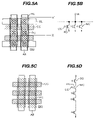
- FIGS. 5A to 5D are plan views and equivalent circuit diagrams schematically showing the structures of flash memory cells.
- FIGS. 6A to 6U are cross sectional views of a semiconductor device schematically illustrating manufacture processes for a semiconductor device mixedly mounting flash memory cells and other transistors according to a fifth embodiment of the present invention.
- FIGS. 7A to 7E are cross sectional views of a semiconductor substrate schematically illustrating a manufacture method for a semiconductor device according to prior art.
- FIGS. 8A to 8D are cross sectional views of a semiconductor substrate schematically illustrating a manufacture method for a semiconductor device mixedly mounting flash memory cells and other transistors according to prior art.
- FIGS. 1A to 1E are cross sectional views schematically illustrating a manufacture method for a semiconductor device according to the first embodiment of the present invention.
- an isolation trench is formed in the surface layer of, e.g., a p-type semiconductor substrate 11 , an insulating film is buried in the trench, and an unnecessary portion of the insulating film is removed by chemical mechanical polishing (CMP) to form an STI type isolation region 12 .
- CMP chemical mechanical polishing
- the surface of each active region defined by the isolation region 12 is thermally oxidized at 800° C. to 1100° C. to form a gate insulating film 13 .
- a polysilicon film is deposited on the surface of the semiconductor substrate, covering the gate oxide film 13 . By using a photoresist pattern as a mask, the polysilicon film is etched to pattern a gate electrode 14 .
- mixture gas of HBr and Cl 2 is used as etching gas to perform reactive ion etching (RIE) having a high selectivity with considerably different etching rates between silicon and the silicon oxide film.
- RIE reactive ion etching
- This etching has a very slow etching rate of the silicon oxide film relative to Si. Therefore, while polysilicon is etched, etching can be stopped by only slightly etching the gate oxide film 13 .
- the resist pattern is thereafter removed.
- the patterned gate electrode as a mask, for example, n-type impurity ions are implanted shallowly to form extension regions 15 of source/drain regions.
- a silicon nitride film is deposited covering the gate electrode, and thereafter etched back to leave side wall spacers 16 of the silicon nitride film only on the side walls of the gate electrode 14 .
- This etching is performed by reactive ion etching (RIE) using mainly CHF 3 as etching gas to leave the gate oxide film 13 . If damages to the substrate poses no problem, the gate oxide film 13 may be etched and removed.
- RIE reactive ion etching
- silicon oxide is isotropically etched. Irotropic etching is an etching method with smaller damages, and can be performed by using dilute hydrofluoric acid solution or downstream dry etching. Since isotropic etching progresses also along a lateral direction, the gate insulating film 13 under the side wall spacers 16 is retracted. In this manner, undercuts are formed under the side wall spacers 16 .
- a silicon oxide film 23 is deposited on the whole surface of the substrate by using tetraethoxysilane (TEOS).
- TEOS tetraethoxysilane
- the silicon oxide film 23 is deposited on the whole surface of the substrate, burying also the undercuts.
- Anisotropic etching is performed by RIE using mainly CF 4 as etching gas.
- the silicon oxide film on a flat surface is removed to form side wall spacers 23 of the silicon oxide film which covers the side surfaces of the side wall spacers 16 of the silicon nitride film and burying the undercuts.
- the silicon oxide films on the surface of the semiconductor substrate 11 and on the surface of the gate electrode 14 are removed with dilute hydrofluoric acid solution to expose clean surfaces. Since the whole side surfaces of the side wall spacers are made of the TEOS silicon oxide film, an etching rate is uniform and undercuts will not be formed. It is therefore possible to prevent an unexpected short circuit and strain.
- a metal layer capable of being silicidated such as a Co layer and a Ti layer is formed on the surface of the semiconductor substrate to a thickness of, e.g., about 30 nm by sputtering.
- a primary silicidation reaction is performed by rapid thermal annealing (RTA), for example, 30 seconds at 550° C. to conduct the primary silicidation reaction between Si and metal.
- RTA rapid thermal annealing
- a secondary silicidation reaction is performed by RTA, for example, 30 seconds at 800° C. to form silicide layers 18 .
- FIGS. 2A to 2E are cross sectional views schematically illustrating a semiconductor device manufacture method according to the second embodiment of the present invention.
- FIGS. 2A and 2B show the same structures as those shown in FIGS. 1A and 1B , and these structures can be manufactured by the same processes.
- side wall spacers 23 of TEOS silicon oxide are formed covering the side wall spacers 16 of silicon nitride.
- the TEOS silicon oxide film has an etching rate faster than that of the thermally oxidized film. While the side wall spacers 23 are formed, control etching is performed to leave the gate oxide film 13 .
- the surfaces of the substrate 11 and gate electrode 14 are exposed by using dilute hydrofluoric acid solution.
- the TEOS silicon oxide film 23 has an etching rate faster than that of the thermally oxidized gate oxide film 13 . Therefore, when the gate oxide film 13 and TEOS silicon oxide film 23 are etched at the same time, etching the gate oxide film 13 is delayed so that undercuts will not be formed even if projections are formed.
- silicide layers 18 are formed on the exposed silicon surfaces similar to the first embodiment.
- the gate oxide film is exposed in the area lower than the side wall spacers.
- the outermost layers of the side wall spacers is made of the silicon oxide film having an etching rate faster than that of the gate oxide film, undercuts will not be formed.
- the side wall spacers contain the silicon nitride films so that the SAC process can be executed. The silicon nitride film does not contact the substrate surface so that excessive strain is prevented from being applied.
- FIGS. 3A to 3E are cross sectional views schematically illustrating a semiconductor device manufacture method according to the third embodiment of the present invention.
- FIG. 3A shows the same structure as that shown in FIG. 1A , and this structure can be manufactured by the same process.
- a silicon oxide film made of TEOS and a silicon nitride film are successively deposited covering the gate electrode 14 , etched back to form laminated side wall spacers made of silicon oxide films 24 covering the side walls of the gate electrode 14 and silicon nitride films 16 on the silicon oxide films 24 .
- a silicon oxide film formed by thermal oxidation may be used.
- the silicon nitride film is etched by using mainly CHF 3 gas as etching gas, and the silicon oxide film is etched mainly by using CF 4 gas as etching gas. If the gate oxide film 2 is to be left, control etching with limited time is performed.
- the gate oxide film or a native or natural oxide film on the silicon surface is removed by using dilute hydrofluoric acid solution to expose the surface of the active region. Since the silicon oxide film on the substrate surface, the gate oxide film 13 and the silicon oxide films 24 of the side wall spacers are etched, undercuts are formed under the silicon nitride side wall spacers 16 .
- a silicon oxide film of TEOS is deposited and etched back to form side wall spacers 23 .
- the side wall spacers 23 bury the undercuts under the side wall spacers of the silicon nitride film to form an outer surface without undercuts.
- silicide layers 18 are formed on the exposed silicon surfaces.
- the side wall spacer is made of three layers including the silicon oxide film, silicon nitride film and silicon oxide film and the outermost side wall spacers 23 reach the substrate surfaces.
- the dilute hydrofluoric acid washing process before the silicide layers are formed can therefore prevent undercuts from being formed. Since the side wall spacers contain the silicon nitride films, the SAC process can be executed. The silicon nitride film does not contact the substrate surface, so that excessive strain is prevented from being applied.
- FIGS. 4A to 4E are cross sectional views schematically illustrating a semiconductor device manufacture method according to the fourth embodiment of the present invention.
- FIG. 4A shows the same structure as that shown in FIG. 1A , and this structure can be manufactured by the same process.
- a lamination of a silicon oxide film 24 and a silicon nitride film 16 is deposited covering the gate electrode 14 , and the silicon nitride film 16 is etched back.
- RIE reactive ion etching gas
- a silicon oxide film 23 is deposited on the whole substrate surface, and etched back to remove the silicon oxide films 23 and 24 on the flat surface.
- Side wall spacers are therefore formed on the side walls of the gate electrode 14 , each having a three-layer lamination structure of the silicon oxide film 24 , silicon nitride film 16 and silicon oxide film 23 .
- the first silicon oxide films 24 in a bent shape or L-shape are formed on the upper surface of the gate oxide film 13 and on the side walls of the gate electrodes 14 , and side wall spacers made of a lamination of the silicon nitride films 16 and silicon oxide films 23 are formed on the bent first silicon oxide films.
- ion implantation is performed to form source/drain regions 17 .
- a gate oxide film or a natural or na ⁇ ve oxide film existing on the silicon substrate surface is removed to expose a clean substrate surface. Although the side surfaces of the gate oxide film are exposed, the gate oxide film has an etching rate slower than that of the silicon oxide film 23 and undercuts will not be formed.
- a silicidation reaction like that shown in FIG. 1E is performed to form silicide layers 18 on exposed silicon surfaces.
- the silicide layers of low resistance are formed on the silicon surfaces, without undercuts so that the resistance of the electrode regions can be lowered.
- the etching rate of the gate oxide film is slower than that of the upper silicon oxide film and the side etching is suppressed so that undercuts are prevented from being formed.
- the side wall spacers contain the silicon nitride film, i.e., an insulating film having a barrier function, the SAC process of etching the interlayer insulating film can be executed. The silicon nitride film does not reach the substrate surface so that excessive strain can be prevented from being applied.
- FIGS. 5A and 5B are a plan view and an equivalent circuit diagram showing the structure of a NOR type flash memory.
- an isolation region ISO is formed in a semiconductor substrate to define active regions AR.
- a tunneling oxide film is formed on the active region AR, and an amorphous silicon film as a floating gate and an ONO film are deposited on the whole substrate surface and patterned in conformity with the shape of the active region AR.
- a polysilicon film as a control gate is deposited and patterned along a direction perpendicular to the floating gate, and the exposed underlying ONO film and floating gate are patterned. Ion implantation for source/drain regions is performed to form a fundamental structure of a flash memory.
- a source line SL is formed along a direction crossing the active region AR, and connected to source regions.
- a bit line BL is formed on the interlayer insulating film along a direction along the active region, and connected to drain regions.
- each flash memory cell MC having the floating gate FG and control gate CG is connected to a common bit line BL and a separate source line so that each flash memory can be read independently.
- FIGS. 5C and 5D is a plane view and an equivalent circuit diagram showing the structure of a NAND type flash memory.
- an isolation region ISO is formed to define active regions AR along a vertical direction in FIG. 5C similar to FIG. 5A .
- a floating gate FG is formed along a direction along the active region AR, and a control gate CG is formed along a direction crossing the direction of the floating gate, and patterned together with the underlying floating gate FG.
- a plurality of flash memory cells MC are connected in series and connected to a read circuit via a select gate SG.
- An on-voltage is applied to the select gate SG, a read voltage for turning on/off a cell in accordance with accumulated charges is applied to the cell, and an on-voltage is applied to other flash memory cells MC to forcibly turn on these cells.
- a storage state of a memory cell can be read via a plurality of transistors.
- a tunneling oxide film 25 having a thickness of 8 nm to 10 nm is formed on the surface of an active region of a semiconductor substrate 11 by thermal oxidation at 800° C. to 1000° C.
- the left area is a memory area in which a flash memory is formed
- the central area is a logic circuit area in which low voltage operation transistors are formed
- the right area is a peripheral circuit area in which high voltage operation transistors are formed.
- a plurality of types of transistors having different gate oxide film thicknesses may be formed in the logic circuit area. Each area is defined by an isolation region such as STI.
- a doped amorphous silicon film having a thickness of 80 nm to 120 nm and a P concentration of about 5E19 (5 ⁇ 10 19 ) cm ⁇ 3 is deposited on the tunneling oxide film 25 by CVD at about 500° C., and an ONO film 27 is formed on the doped amorphous silicon film.
- the doped amorphous silicon film is changed to a polysilicon film at a later heat treatment.
- the ONO film is made of a lamination of a silicon oxide film 27 a , a silicon nitride film 27 b and a silicon oxide film 27 c .
- the silicon oxide film 27 a having a thickness of 5 nm to 10 nm is deposited on the amorphous silicon film 27 by high temperature CVD at a substrate temperature of 750° C. or higher, e.g., 800° C.
- the silicon nitride film 27 b having a thickness of 5 nm to 10 nm is formed on the silicon oxide film 27 a by low pressure CVD at a temperature of, e.g., 700° C. or higher.
- the surface of the silicon nitride film 27 b is thermally oxidized at 950° C. to form the thermally oxidized silicon film 27 c having a thickness of 3 nm to 10 nm.
- the ONO film 27 formed in this manner has an excellent leak current preventive function. Although a film forming temperature of 700° C. or higher is adopted, this poses no problem because diffusion regions are still not formed in the transistor area.
- the ONO film 27 , silicon film 26 and tunneling oxide film 25 in the low and high voltage operation transistor areas are removed. These films on the isolation region are also removed.
- the tunneling oxide film 25 is removed by wet etching using dilute HF solution.
- a silicon oxide film 13 a is formed on the surface of the substrate 11 by thermal oxidation at 800° C. to 1100° C., the film 13 a having a thickness of 10 nm to 50 nm suitable for a gate oxide film of a high voltage transistor.
- a similar silicon oxide film is also formed in the low voltage operation transistor area. Oxidation will not progress in the flash memory cell area because it is covered with the ONO film 27 .
- a resist mask PR 2 is formed covering the flash memory cell area and high voltage operation transistor area, and the silicon oxide film 13 a in the low voltage operation transistor area is removed by using dilute hydrofluoric acid solution.
- a gate oxide film 13 b having a thickness of 1 nm to 10 nm is formed on the surface of the low voltage operation transistor area by thermal oxidation at 800° C. to 1100° C. In this manner, a thin gate oxide film is formed in the low voltage operation transistor area and a thick gate oxide film is formed in the high voltage operation transistor area.
- the gate oxide films of transistors may by made of silicon oxynitride instead of silicon oxide.
- a polysilicon film 28 is deposited on the substrate surface to a thickness of 80 nm to 250 nm by CVD at a substrate temperature of, e.g., 620° C.
- This polysilicon film 28 is patterned in a later process to form a control gate electrode of the flash memory cell and a gate electrode in the transistor area.
- a silicon nitride film 34 having a thickness of 10 nm to 25 nm is formed on the polysilicon film 28 by plasma CVD at a substrate temperature of, e.g., 400° C.
- a thermal silicon nitride film or a silicon oxynitride film by plasma CVD may be formed.
- the silicon nitride film is not necessary to be highly dense and have a high quality, if it functions as an etch stopper and a mask for thermal oxidation and ion implantation.
- a resist pattern PR 3 is formed on the silicon nitride film 34 , having a laminated gate structure pattern of the flash memory cell and covering the low and high voltage operation transistor areas. Etched by using this resist pattern PR 3 as a mask are the plasma silicon nitride film 34 , polysilicon film 28 , ONO film 27 and silicon film 26 . Patterned in the flash memory cell area are the floating gate electrode 26 of the silicon film, ONO film 27 , control gate electrode 28 c and plasma silicon nitride film 34 . The resist pattern PR 3 is thereafter removed.
- a protective oxide film 35 having a thickness of 1 nm to 5 nm is formed on the side planes of the silicon film of the flash memory cell by thermal oxidation at 800° C. to 900° C.
- the thermally oxidized film is an insulating film having a high barrier function relative to carrier leak. Thermal oxidation will not progress in the low and high voltage operation transistor areas because the silicon nitride film 34 covers the polysilicon film 28 .
- a resist pattern PR 4 is formed covering one side of the gate electrode of the flash memory cell and the low and high voltage operation transistor areas.
- P + ions are implanted into the region exposed in the opening of the resist pattern PR 4 under the conditions of an acceleration energy of 50 keV to 80 keV and a dose of 1 ⁇ 10 14 cm ⁇ 2 to 5 ⁇ 10 14 cm ⁇ 2 , to thereby form a n-type drain region 31 .
- As + ions are implanted to form a diffusion region 32 under the conditions of an acceleration energy of 30 keV to 50 keV and a dose of 1 ⁇ 10 15 cm ⁇ 2 to 6 ⁇ 10 15 cm ⁇ 2 .
- the resist pattern PR 4 is thereafter removed.
- a resist pattern PR 5 is formed covering the low and high voltage operation transistor areas. As + ions are implanted into the flash memory area under the conditions of an acceleration energy of 20 keV to 60 keV and a dose of 5 ⁇ 10 14 cm ⁇ 2 to 3 ⁇ 10 15 cm ⁇ 2 to raise the concentration of the diffusion region 32 and form a source diffusion region 33 on the other side. The resist pattern PR 5 is thereafter removed.
- a TEOS silicon oxide film 36 is deposited at a substrate temperature of 600° C., and then a silicon nitride film 37 is deposited by low pressure (LP) CVD at 0.8 torr and a substrate temperature of 800°.
- the silicon nitride film formed by LP-CVD is a highly dense and high quality insulating film having a high barrier function relative to moisture and SiH bases.
- the LP-CVD silicon nitride film and TEOS silicon oxide film are removed by anisotropic etching using mainly CHF 3 as etching gas and anisotropic etching using mainly CF 4 as etching gas, respectively, to form side wall spacers made of a lamination of the silicon oxide film 36 and silicon nitride film 37 on the side walls of the laminated gate electrode.
- the TEOS silicon oxide film 36 may be omitted.
- anisotropic etching is further performed by using mainly CF 4 as etching gas to etch the silicon nitride film 34 .
- the upper portion of the side wall spacers 37 of silicon nitride is also etched.
- the silicon nitride film 34 in the transistor area is also etched and the silicon film 28 is exposed.
- etching the silicon nitride films 37 and 34 may be performed successively.
- a resist pattern PR 6 is formed having a gate electrode pattern in the transistor area and covering the flash memory area.
- the resist pattern PR 6 is etched to form gate electrodes 28 a and 28 b . Since the silicon nitride film 34 was removed, the layer to be etched is only a silicon layer so that high precision etching becomes easy.
- the resist pattern PR 6 is thereafter removed.
- a resist pattern PR 7 is formed covering the flash memory area and high voltage operation transistor area, and n-type impurity ions are implanted into the low voltage operation transistor area to form extension regions 41 of source/drain regions.
- the resist pattern PR 7 is thereafter removed.
- a resist pattern PR 8 is formed covering the flash memory cell area and low voltage operation transistor area.
- Lightly doped drain (LDD) regions 42 are formed by implanting n-type impurity ions into the high voltage operation transistor area.
- the resist pattern PR 8 is thereafter removed. If the conditions are satisfied, extension regions and LDD regions may be formed by the same ion implantation process without separating the low and high voltage operation transistor areas.
- a TEOS silicon oxide film 44 is deposited on the whole substrate surface to a thickness of 80 nm to 150 nm at a substrate temperature of 600° C., and etched back to remove the silicon oxide film on the flat surface.
- Side wall spacers 44 c of silicon oxide are formed on the side walls of the laminated gate electrode in the flash memory cell area, whereas side wall spacers 44 b and 44 a of silicon oxide are formed on the side walls of the gate electrodes 28 b and 28 a in the low and high voltage operation transistor areas.
- n-type impurity ions are implanted into all active regions to form source/drain regions 46 .
- CMOS circuit If a CMOS circuit is to be formed, p-channel regions and n-channel regions are separated by resist patterns and n-type and p-type impurity ions are implanted.
- the substrate surface and gate electrode surfaces are washed with dilute hydrofluoric acid solution to remove a natural oxide film and the like, and thereafter a metal layer capable of silicidation such as Ti and Co is deposited to a thickness of about 30 nm by sputtering. If necessary, a TiN layer is further deposited and annealing is performed, for example, for 30 seconds at 500° C. to form primary silicide layers. After an unreacted metal layer and the like are removed, secondary annealing is performed, for example, for 30 seconds at 800° C. to form silicide layers 18 having a low resistance.
- a metal layer capable of silicidation such as Ti and Co is deposited to a thickness of about 30 nm by sputtering.
- a TiN layer is further deposited and annealing is performed, for example, for 30 seconds at 500° C. to form primary silicide layers.
- secondary annealing is performed, for example, for 30 seconds at 800° C. to form silicide layers
- the silicon nitride layer does not expose on the surfaces of the side wall spacers, and the gate oxide film and TEOS silicon oxide film expose in contact with the substrate. Therefore, undercuts will not be formed and there is no problem of short circuits, strain and the like.
- an interlayer insulating film 21 is deposited covering the gate electrode structures, and the surface thereof is planarized if necessary.
- Contact holes are formed through the interlayer insulating film 21 , and after a Ti layer, a TiN layer and the like are formed, a W layer is deposited burying the contact holes, and an unnecessary portion is removed to form W plugs 22 .
- a semiconductor device mixedly integrating a plurality of types of semiconductor elements is formed.
- upper level wirings are formed to form a multi-layer wiring structure.
- General techniques of semiconductor devices may adopt various well-known techniques (for example, refer to U.S. Pat. Nos. 6,492,734 and 6,500,710, the entire contents of which are incorporated herein by reference).
- the present invention is applicable to semiconductor devices.
- the present invention is applicable to a semiconductor integrated circuit device mixedly mounting a plurality of types of semiconductor devices.
Abstract
Description
Claims (7)
Priority Applications (1)
| Application Number | Priority Date | Filing Date | Title |
|---|---|---|---|
| US12/007,420 US7511331B2 (en) | 2003-10-23 | 2008-01-10 | Semiconductor device having side wall spacers |
Applications Claiming Priority (3)
| Application Number | Priority Date | Filing Date | Title |
|---|---|---|---|
| PCT/JP2003/013582 WO2005041307A1 (en) | 2003-10-23 | 2003-10-23 | Semiconductor device and method for manufacturing semiconductor device |
| US11/390,128 US20060163678A1 (en) | 2003-10-23 | 2006-03-28 | Semiconductor device and method for manufacturing semiconductor device |
| US12/007,420 US7511331B2 (en) | 2003-10-23 | 2008-01-10 | Semiconductor device having side wall spacers |
Related Parent Applications (1)
| Application Number | Title | Priority Date | Filing Date |
|---|---|---|---|
| US11/390,128 Division US20060163678A1 (en) | 2003-10-23 | 2006-03-28 | Semiconductor device and method for manufacturing semiconductor device |
Publications (2)
| Publication Number | Publication Date |
|---|---|
| US20080142871A1 US20080142871A1 (en) | 2008-06-19 |
| US7511331B2 true US7511331B2 (en) | 2009-03-31 |
Family
ID=34509571
Family Applications (2)
| Application Number | Title | Priority Date | Filing Date |
|---|---|---|---|
| US11/390,128 Abandoned US20060163678A1 (en) | 2003-10-23 | 2006-03-28 | Semiconductor device and method for manufacturing semiconductor device |
| US12/007,420 Expired - Fee Related US7511331B2 (en) | 2003-10-23 | 2008-01-10 | Semiconductor device having side wall spacers |
Family Applications Before (1)
| Application Number | Title | Priority Date | Filing Date |
|---|---|---|---|
| US11/390,128 Abandoned US20060163678A1 (en) | 2003-10-23 | 2006-03-28 | Semiconductor device and method for manufacturing semiconductor device |
Country Status (6)
| Country | Link |
|---|---|
| US (2) | US20060163678A1 (en) |
| EP (2) | EP1677359A4 (en) |
| JP (1) | JP4866609B2 (en) |
| CN (1) | CN100461449C (en) |
| AU (1) | AU2003275625A1 (en) |
| WO (1) | WO2005041307A1 (en) |
Cited By (5)
| Publication number | Priority date | Publication date | Assignee | Title |
|---|---|---|---|---|
| US20100295137A1 (en) * | 2006-03-24 | 2010-11-25 | Xianfeng Zhou | Method and apparatus providing different gate oxides for different transitors in an integrated circuit |
| US20170186616A1 (en) * | 2013-12-05 | 2017-06-29 | Taiwan Semiconductor Manufacturing Company, Ltd. | Spacers with Rectangular Profile and Methods of Forming the Same |
| US20180190787A1 (en) * | 2014-06-19 | 2018-07-05 | Globalfoundries Inc. | Method and structure for protecting gates during epitaxial growth |
| US20180211966A1 (en) * | 2016-08-16 | 2018-07-26 | United Microelectronics Corp. | Method for fabricating semiconductor structure |
| US11653498B2 (en) | 2017-11-30 | 2023-05-16 | Taiwan Semiconductor Manufacturing Co., Ltd. | Memory device with improved data retention |
Families Citing this family (29)
| Publication number | Priority date | Publication date | Assignee | Title |
|---|---|---|---|---|
| KR100526478B1 (en) * | 2003-12-31 | 2005-11-08 | 동부아남반도체 주식회사 | Semiconductor device and fabricating method thereof |
| US7253114B2 (en) * | 2005-03-16 | 2007-08-07 | Taiwan Semiconductor Manufacturing Company | Self-aligned method for defining a semiconductor gate oxide in high voltage device area |
| US8629490B2 (en) * | 2006-03-31 | 2014-01-14 | Semiconductor Energy Laboratory Co., Ltd. | Nonvolatile semiconductor storage device with floating gate electrode and control gate electrode |
| JP4928825B2 (en) * | 2006-05-10 | 2012-05-09 | ルネサスエレクトロニクス株式会社 | Manufacturing method of semiconductor device |
| KR100845720B1 (en) * | 2006-11-30 | 2008-07-10 | 동부일렉트로닉스 주식회사 | Flash Memory Device and Method of Manufactruing the same |
| US7871885B2 (en) * | 2006-12-20 | 2011-01-18 | Dongbu Hitek Co., Ltd. | Manufacturing method of flash memory device |
| KR100786707B1 (en) * | 2006-12-21 | 2007-12-18 | 삼성전자주식회사 | Non-volatile memory device and method of manufacturing the same |
| KR100842661B1 (en) * | 2006-12-27 | 2008-06-30 | 동부일렉트로닉스 주식회사 | Flash memory device and method of manufacturing the same |
| US7528076B2 (en) * | 2007-05-11 | 2009-05-05 | United Microelectronics Corp. | Method for manufacturing gate oxide layer with different thicknesses |
| US7960243B2 (en) * | 2007-05-31 | 2011-06-14 | Freescale Semiconductor, Inc. | Method of forming a semiconductor device featuring a gate stressor and semiconductor device |
| JP2009016462A (en) * | 2007-07-03 | 2009-01-22 | Renesas Technology Corp | Semiconductor device and its manufacturing method |
| KR101191818B1 (en) * | 2007-07-31 | 2012-10-16 | 후지쯔 세미컨덕터 가부시키가이샤 | Semiconductor device and its manufacturing method |
| US7960267B2 (en) * | 2009-03-31 | 2011-06-14 | Freescale Semiconductor, Inc. | Method for making a stressed non-volatile memory device |
| JP2011060989A (en) * | 2009-09-10 | 2011-03-24 | Toshiba Corp | Method of manufacturing semiconductor device |
| JP2011066038A (en) * | 2009-09-15 | 2011-03-31 | Toshiba Corp | Semiconductor memory device |
| US8030154B1 (en) * | 2010-08-03 | 2011-10-04 | International Business Machines Corporation | Method for forming a protection layer over metal semiconductor contact and structure formed thereon |
| JP6059566B2 (en) | 2012-04-13 | 2017-01-11 | 株式会社半導体エネルギー研究所 | Method for manufacturing semiconductor device |
| US8995607B2 (en) | 2012-05-31 | 2015-03-31 | Semiconductor Energy Laboratory Co., Ltd. | Pulse signal output circuit and shift register |
| US8822319B2 (en) * | 2012-09-12 | 2014-09-02 | Ememory Technology Inc. | Method of manufacturing non-volatile memory |
| KR20140052763A (en) * | 2012-10-25 | 2014-05-07 | 삼성전자주식회사 | Semiconductor devices having a gate structure and methods of fabricating the same |
| US8877585B1 (en) * | 2013-08-16 | 2014-11-04 | Freescale Semiconductor, Inc. | Non-volatile memory (NVM) cell, high voltage transistor, and high-K and metal gate transistor integration |
| CN104347515B (en) * | 2013-08-01 | 2018-04-03 | 中芯国际集成电路制造(上海)有限公司 | A kind of preparation method of flash memories |
| CN104882479B (en) * | 2014-02-28 | 2018-02-27 | 无锡华润上华科技有限公司 | A kind of HVPMOS devices and its manufacture method |
| CN104882412B (en) * | 2014-02-28 | 2018-02-13 | 中芯国际集成电路制造(上海)有限公司 | Embedded logical formula flush memory device and its formation method for side wall |
| KR20150146409A (en) | 2014-06-20 | 2015-12-31 | 가부시키가이샤 한도오따이 에네루기 켄큐쇼 | Semiconductor device, display device, input/output device, and electronic device |
| US9922881B2 (en) * | 2016-01-12 | 2018-03-20 | United Microelectronics Corp. | Method for fabricating semiconductor device structure and product thereof |
| JP6649216B2 (en) * | 2016-09-16 | 2020-02-19 | 株式会社東芝 | Semiconductor device and manufacturing method thereof |
| CN108598002B (en) * | 2018-05-15 | 2019-06-28 | 长江存储科技有限责任公司 | MOS transistor and its manufacturing method |
| GB2591472B (en) * | 2020-01-28 | 2022-02-09 | X Fab France Sas | Method of forming asymmetric differential spacers for optimized MOSFET performance and optimized mosfet and SONOS co-integration |
Citations (14)
| Publication number | Priority date | Publication date | Assignee | Title |
|---|---|---|---|---|
| JPH04158530A (en) | 1990-10-23 | 1992-06-01 | Oki Electric Ind Co Ltd | Fabrication of semiconductor element |
| US5352620A (en) | 1984-05-23 | 1994-10-04 | Hitachi, Ltd. | Method of making semiconductor device with memory cells and peripheral transistors |
| US5468987A (en) | 1991-03-06 | 1995-11-21 | Semiconductor Energy Laboratory Co., Ltd. | Semiconductor device and method for forming the same |
| JPH09162396A (en) | 1995-12-11 | 1997-06-20 | Nec Corp | Semiconductor device manufacturing method |
| US5753546A (en) | 1995-06-30 | 1998-05-19 | Hyundai Electronics Industries Co., Ltd. | Method for fabricating metal oxide field effect transistors |
| JPH10321738A (en) | 1997-05-21 | 1998-12-04 | Ricoh Co Ltd | Nonvolatile semiconductor memory device and its manufacturing method |
| US6344388B1 (en) | 1998-12-25 | 2002-02-05 | Mitsubishi Denki Kabushiki Kaisha | Method of manufacturing semiconductor device |
| US20020041000A1 (en) | 2000-10-11 | 2002-04-11 | Hiroshi Watanabe | Semiconductor device and method of manufacturing the same |
| JP2003023114A (en) | 2001-07-05 | 2003-01-24 | Fujitsu Ltd | Semiconductor integrated circuit device and its manufacturing method |
| WO2003012878A1 (en) | 2001-07-27 | 2003-02-13 | Renesas Technology Corp. | Semiconductor device |
| US20030067045A1 (en) | 2001-10-04 | 2003-04-10 | Fujitsu Limited | Semiconductor device and method of manufacturing the same |
| KR20030076266A (en) | 2002-03-22 | 2003-09-26 | 가부시키가이샤 히타치세이사쿠쇼 | Mis semiconductor device and manufacturing method thereof |
| US6815288B2 (en) * | 2000-05-30 | 2004-11-09 | Samsung Electronics Co., Ltd. | Merged memory and logic semiconductor device of salicided dual gate structure including embedded memory of self-aligned contact structure and manufacturing method thereof |
| US6906360B2 (en) | 2003-09-10 | 2005-06-14 | International Business Machines Corporation | Structure and method of making strained channel CMOS transistors having lattice-mismatched epitaxial extension and source and drain regions |
Family Cites Families (19)
| Publication number | Priority date | Publication date | Assignee | Title |
|---|---|---|---|---|
| JPH03276729A (en) * | 1990-03-27 | 1991-12-06 | Matsushita Electron Corp | Mos-type semiconductor device and manufacture thereof |
| JPH04284675A (en) * | 1991-03-13 | 1992-10-09 | Ricoh Co Ltd | Manufacture of semiconductor device |
| TW223178B (en) * | 1992-03-27 | 1994-05-01 | Semiconductor Energy Res Co Ltd | Semiconductor device and its production method |
| JP3238556B2 (en) * | 1993-12-06 | 2001-12-17 | 株式会社東芝 | Nonvolatile semiconductor memory device |
| JPH10303141A (en) * | 1997-04-28 | 1998-11-13 | Sony Corp | Semiconductor device and its manufacture |
| JP3113240B2 (en) * | 1999-02-24 | 2000-11-27 | 株式会社東芝 | Nonvolatile semiconductor memory device and method of manufacturing the same |
| JP3240999B2 (en) * | 1998-08-04 | 2001-12-25 | 日本電気株式会社 | Semiconductor memory device and method of manufacturing the same |
| JP2000091265A (en) * | 1998-09-08 | 2000-03-31 | Nec Kyushu Ltd | Semiconductor device and its manufacture |
| JP2000114522A (en) * | 1998-10-08 | 2000-04-21 | Toshiba Corp | Semiconductor device and its manufacture |
| JP3464414B2 (en) | 1999-06-15 | 2003-11-10 | 富士通株式会社 | Nonvolatile semiconductor memory device and method of manufacturing the same |
| JP2001044138A (en) * | 1999-07-28 | 2001-02-16 | Hitachi Ltd | Manufacture of semiconductor integrated circuit device and semiconductor integrated circuit device |
| US6268640B1 (en) * | 1999-08-12 | 2001-07-31 | International Business Machines Corporation | Forming steep lateral doping distribution at source/drain junctions |
| JP2001237421A (en) * | 2000-02-24 | 2001-08-31 | Toshiba Corp | Semiconductor device, sram and method of manufacturing the same |
| JP3544535B2 (en) * | 2000-09-18 | 2004-07-21 | 松下電器産業株式会社 | Semiconductor device and manufacturing method thereof |
| JP4523194B2 (en) | 2001-04-13 | 2010-08-11 | 富士通セミコンダクター株式会社 | Semiconductor device and manufacturing method thereof |
| JP2003124338A (en) * | 2001-10-09 | 2003-04-25 | Sharp Corp | Semiconductor device and its manufacturing method |
| KR100398874B1 (en) * | 2001-11-21 | 2003-09-19 | 삼성전자주식회사 | MOS Transistor With T-Shaped Gate Electrode And Method Of Fabricating The Same |
| JP2003204063A (en) * | 2002-01-10 | 2003-07-18 | Toshiba Corp | Semiconductor device and its manufacturing method |
| US6991979B2 (en) * | 2003-09-22 | 2006-01-31 | International Business Machines Corporation | Method for avoiding oxide undercut during pre-silicide clean for thin spacer FETs |
-
2003
- 2003-10-23 JP JP2005509848A patent/JP4866609B2/en not_active Expired - Fee Related
- 2003-10-23 AU AU2003275625A patent/AU2003275625A1/en not_active Abandoned
- 2003-10-23 EP EP03758843A patent/EP1677359A4/en not_active Withdrawn
- 2003-10-23 WO PCT/JP2003/013582 patent/WO2005041307A1/en not_active Application Discontinuation
- 2003-10-23 CN CNB2003801104559A patent/CN100461449C/en not_active Expired - Fee Related
- 2003-10-23 EP EP08162077.5A patent/EP1986240B1/en not_active Expired - Fee Related
-
2006
- 2006-03-28 US US11/390,128 patent/US20060163678A1/en not_active Abandoned
-
2008
- 2008-01-10 US US12/007,420 patent/US7511331B2/en not_active Expired - Fee Related
Patent Citations (16)
| Publication number | Priority date | Publication date | Assignee | Title |
|---|---|---|---|---|
| US5352620A (en) | 1984-05-23 | 1994-10-04 | Hitachi, Ltd. | Method of making semiconductor device with memory cells and peripheral transistors |
| JPH04158530A (en) | 1990-10-23 | 1992-06-01 | Oki Electric Ind Co Ltd | Fabrication of semiconductor element |
| US5468987A (en) | 1991-03-06 | 1995-11-21 | Semiconductor Energy Laboratory Co., Ltd. | Semiconductor device and method for forming the same |
| US5753546A (en) | 1995-06-30 | 1998-05-19 | Hyundai Electronics Industries Co., Ltd. | Method for fabricating metal oxide field effect transistors |
| JPH09162396A (en) | 1995-12-11 | 1997-06-20 | Nec Corp | Semiconductor device manufacturing method |
| JPH10321738A (en) | 1997-05-21 | 1998-12-04 | Ricoh Co Ltd | Nonvolatile semiconductor memory device and its manufacturing method |
| US6344388B1 (en) | 1998-12-25 | 2002-02-05 | Mitsubishi Denki Kabushiki Kaisha | Method of manufacturing semiconductor device |
| US6815288B2 (en) * | 2000-05-30 | 2004-11-09 | Samsung Electronics Co., Ltd. | Merged memory and logic semiconductor device of salicided dual gate structure including embedded memory of self-aligned contact structure and manufacturing method thereof |
| US20020041000A1 (en) | 2000-10-11 | 2002-04-11 | Hiroshi Watanabe | Semiconductor device and method of manufacturing the same |
| JP2003023114A (en) | 2001-07-05 | 2003-01-24 | Fujitsu Ltd | Semiconductor integrated circuit device and its manufacturing method |
| WO2003012878A1 (en) | 2001-07-27 | 2003-02-13 | Renesas Technology Corp. | Semiconductor device |
| US20050258474A1 (en) | 2001-07-27 | 2005-11-24 | Toshihiro Tanaka | Semiconductor device |
| US20030067045A1 (en) | 2001-10-04 | 2003-04-10 | Fujitsu Limited | Semiconductor device and method of manufacturing the same |
| KR20030076266A (en) | 2002-03-22 | 2003-09-26 | 가부시키가이샤 히타치세이사쿠쇼 | Mis semiconductor device and manufacturing method thereof |
| US6744099B2 (en) | 2002-05-22 | 2004-06-01 | Hitachi, Ltd. | MIS semiconductor device and manufacturing method thereof |
| US6906360B2 (en) | 2003-09-10 | 2005-06-14 | International Business Machines Corporation | Structure and method of making strained channel CMOS transistors having lattice-mismatched epitaxial extension and source and drain regions |
Non-Patent Citations (5)
| Title |
|---|
| Chinese Office Action dated Mar. 7, 2008, issued in corresponding Chinese Patent Application No. 2003801104559 with English translation. |
| European Search Report dated Oct. 13, 2008; Application No. EP 08162077. |
| International Search Report of International Application PCT/JP2003/013582 mailed Jan. 27, 2004. |
| Office Action dated Feb. 23, 2007, issued in corresponding Korean Application No. 10-2006-7005743. |
| Supplemental European Search Report dated May 23, 2008 issued in corresponding European Application No. EP 03 75 8843. |
Cited By (11)
| Publication number | Priority date | Publication date | Assignee | Title |
|---|---|---|---|---|
| US20100295137A1 (en) * | 2006-03-24 | 2010-11-25 | Xianfeng Zhou | Method and apparatus providing different gate oxides for different transitors in an integrated circuit |
| US8102006B2 (en) * | 2006-03-24 | 2012-01-24 | Micron Technology, Inc. | Different gate oxides thicknesses for different transistors in an integrated circuit |
| US8304307B2 (en) | 2006-03-24 | 2012-11-06 | Micron Technology, Inc. | Method of fabricating different gate oxides for different transistors in an integrated circuit |
| US20170186616A1 (en) * | 2013-12-05 | 2017-06-29 | Taiwan Semiconductor Manufacturing Company, Ltd. | Spacers with Rectangular Profile and Methods of Forming the Same |
| US10505018B2 (en) * | 2013-12-05 | 2019-12-10 | Taiwan Semiconductor Manufacturing Company, Ltd. | Spacers with rectangular profile and methods of forming the same |
| US10868143B2 (en) | 2013-12-05 | 2020-12-15 | Taiwan Semiconductor Manufacturing Company, Ltd. | Spacers with rectangular profile and methods of forming the same |
| US20180190787A1 (en) * | 2014-06-19 | 2018-07-05 | Globalfoundries Inc. | Method and structure for protecting gates during epitaxial growth |
| US10446665B2 (en) * | 2014-06-19 | 2019-10-15 | Globalfoundries Inc. | Method and structure for protecting gates during epitaxial growth |
| US20180211966A1 (en) * | 2016-08-16 | 2018-07-26 | United Microelectronics Corp. | Method for fabricating semiconductor structure |
| US10720440B2 (en) * | 2016-08-16 | 2020-07-21 | United Microelectronics Corp. | Method for fabricating semiconductor structure |
| US11653498B2 (en) | 2017-11-30 | 2023-05-16 | Taiwan Semiconductor Manufacturing Co., Ltd. | Memory device with improved data retention |
Also Published As
| Publication number | Publication date |
|---|---|
| JP4866609B2 (en) | 2012-02-01 |
| US20080142871A1 (en) | 2008-06-19 |
| CN1839479A (en) | 2006-09-27 |
| EP1986240B1 (en) | 2016-03-09 |
| EP1677359A1 (en) | 2006-07-05 |
| EP1677359A4 (en) | 2008-06-25 |
| EP1986240A3 (en) | 2008-11-12 |
| CN100461449C (en) | 2009-02-11 |
| JPWO2005041307A1 (en) | 2007-04-05 |
| AU2003275625A1 (en) | 2005-05-11 |
| EP1986240A2 (en) | 2008-10-29 |
| US20060163678A1 (en) | 2006-07-27 |
| WO2005041307A1 (en) | 2005-05-06 |
Similar Documents
| Publication | Publication Date | Title |
|---|---|---|
| US7511331B2 (en) | Semiconductor device having side wall spacers | |
| US8294236B2 (en) | Semiconductor device having dual-STI and manufacturing method thereof | |
| US6716703B2 (en) | Method of making semiconductor memory device having sources connected to source lines | |
| US20060118855A1 (en) | Method of manufacturing a semiconductor integrated circuit using a selective disposable spacer technique and semiconductor integrated circuit manufactured thereby | |
| KR100368594B1 (en) | Split Gate Flash Memory Device | |
| US6784039B2 (en) | Method to form self-aligned split gate flash with L-shaped wordline spacers | |
| US8952536B2 (en) | Semiconductor device and method of fabrication | |
| JP5454543B2 (en) | Manufacturing method of semiconductor device | |
| US20040147099A1 (en) | Method of producing semiconductor device | |
| WO2006117851A1 (en) | Semiconducteur device and method for manufacturing same | |
| US6818505B2 (en) | Non-volatile semiconductor memory device and manufacturing method thereof | |
| KR100658475B1 (en) | Semiconductor device and method of manufacturing the same | |
| US6569735B2 (en) | Manufacturing method for isolation on non-volatile memory | |
| US8669606B2 (en) | Semiconductor device and method for manufacturing thereof | |
| KR100725477B1 (en) | Semiconductor device and method for manufacturing semiconductor device | |
| JP3860408B2 (en) | Semiconductor device and method for manufacturing semiconductor device | |
| JP2001284557A (en) | Producing method for non-volatile semiconductor memory device | |
| KR20030006962A (en) | Non-volatile semiconductor memory device and manufacturing method thereof | |
| JP5794269B2 (en) | Semiconductor device | |
| KR100486120B1 (en) | Method for forming of mos transistor | |
| KR20050094295A (en) | Flash memory device and method of manufacturing the same |
Legal Events
| Date | Code | Title | Description |
|---|---|---|---|
| AS | Assignment |
Owner name: FUJITSU MICROELECTRONICS LIMITED, JAPAN Free format text: ASSIGNMENT OF ASSIGNORS INTEREST;ASSIGNOR:FUJITSU LIMITED;REEL/FRAME:021976/0089 Effective date: 20081104 Owner name: FUJITSU MICROELECTRONICS LIMITED,JAPAN Free format text: ASSIGNMENT OF ASSIGNORS INTEREST;ASSIGNOR:FUJITSU LIMITED;REEL/FRAME:021976/0089 Effective date: 20081104 |
|
| STCF | Information on status: patent grant |
Free format text: PATENTED CASE |
|
| FEPP | Fee payment procedure |
Free format text: PAYOR NUMBER ASSIGNED (ORIGINAL EVENT CODE: ASPN); ENTITY STATUS OF PATENT OWNER: LARGE ENTITY |
|
| AS | Assignment |
Owner name: FUJITSU SEMICONDUCTOR LIMITED, JAPAN Free format text: CHANGE OF NAME;ASSIGNOR:FUJITSU MICROELECTRONICS LIMITED;REEL/FRAME:024651/0744 Effective date: 20100401 |
|
| FPAY | Fee payment |
Year of fee payment: 4 |
|
| FPAY | Fee payment |
Year of fee payment: 8 |
|
| AS | Assignment |
Owner name: FUJITSU SEMICONDUCTOR LIMITED, JAPAN Free format text: CHANGE OF ADDRESS;ASSIGNOR:FUJITSU SEMICONDUCTOR LIMITED;REEL/FRAME:041188/0401 Effective date: 20160909 |
|
| FEPP | Fee payment procedure |
Free format text: MAINTENANCE FEE REMINDER MAILED (ORIGINAL EVENT CODE: REM.); ENTITY STATUS OF PATENT OWNER: LARGE ENTITY |
|
| LAPS | Lapse for failure to pay maintenance fees |
Free format text: PATENT EXPIRED FOR FAILURE TO PAY MAINTENANCE FEES (ORIGINAL EVENT CODE: EXP.); ENTITY STATUS OF PATENT OWNER: LARGE ENTITY |
|
| STCH | Information on status: patent discontinuation |
Free format text: PATENT EXPIRED DUE TO NONPAYMENT OF MAINTENANCE FEES UNDER 37 CFR 1.362 |
|
| FP | Lapsed due to failure to pay maintenance fee |
Effective date: 20210331 |