US7514743B2 - DMOS transistor with floating poly-filled trench for improved performance through 3-D field shaping - Google Patents
DMOS transistor with floating poly-filled trench for improved performance through 3-D field shaping Download PDFInfo
- Publication number
- US7514743B2 US7514743B2 US11/351,644 US35164406A US7514743B2 US 7514743 B2 US7514743 B2 US 7514743B2 US 35164406 A US35164406 A US 35164406A US 7514743 B2 US7514743 B2 US 7514743B2
- Authority
- US
- United States
- Prior art keywords
- trench portions
- drain
- gate
- floating trench
- dmos
- Prior art date
- Legal status (The legal status is an assumption and is not a legal conclusion. Google has not performed a legal analysis and makes no representation as to the accuracy of the status listed.)
- Expired - Fee Related, expires
Links
- 238000007493 shaping process Methods 0.000 title description 19
- 238000000034 method Methods 0.000 claims description 32
- 210000000746 body region Anatomy 0.000 claims description 31
- 239000000758 substrate Substances 0.000 claims description 24
- 239000002184 metal Substances 0.000 claims description 10
- 239000004065 semiconductor Substances 0.000 claims description 6
- 239000000463 material Substances 0.000 claims description 5
- 229910021420 polycrystalline silicon Inorganic materials 0.000 claims description 4
- 229920005591 polysilicon Polymers 0.000 claims description 4
- 239000004020 conductor Substances 0.000 claims 2
- 230000015556 catabolic process Effects 0.000 abstract description 41
- 230000005684 electric field Effects 0.000 abstract description 10
- 230000008878 coupling Effects 0.000 description 11
- 238000010168 coupling process Methods 0.000 description 11
- 238000005859 coupling reaction Methods 0.000 description 11
- 230000001413 cellular effect Effects 0.000 description 9
- 230000000694 effects Effects 0.000 description 7
- 230000000903 blocking effect Effects 0.000 description 4
- 238000013461 design Methods 0.000 description 4
- XUIMIQQOPSSXEZ-UHFFFAOYSA-N Silicon Chemical compound [Si] XUIMIQQOPSSXEZ-UHFFFAOYSA-N 0.000 description 3
- 238000005094 computer simulation Methods 0.000 description 3
- 229910052710 silicon Inorganic materials 0.000 description 3
- 239000010703 silicon Substances 0.000 description 3
- 230000007480 spreading Effects 0.000 description 3
- VYPSYNLAJGMNEJ-UHFFFAOYSA-N Silicium dioxide Chemical compound O=[Si]=O VYPSYNLAJGMNEJ-UHFFFAOYSA-N 0.000 description 2
- 230000008901 benefit Effects 0.000 description 2
- 238000002955 isolation Methods 0.000 description 2
- 238000012986 modification Methods 0.000 description 2
- 230000004048 modification Effects 0.000 description 2
- 230000003071 parasitic effect Effects 0.000 description 2
- 241001354791 Baliga Species 0.000 description 1
- OAICVXFJPJFONN-UHFFFAOYSA-N Phosphorus Chemical compound [P] OAICVXFJPJFONN-UHFFFAOYSA-N 0.000 description 1
- 238000013459 approach Methods 0.000 description 1
- 239000000969 carrier Substances 0.000 description 1
- 230000008859 change Effects 0.000 description 1
- 229910052681 coesite Inorganic materials 0.000 description 1
- 239000012141 concentrate Substances 0.000 description 1
- 229910052906 cristobalite Inorganic materials 0.000 description 1
- 238000002347 injection Methods 0.000 description 1
- 239000007924 injection Substances 0.000 description 1
- 238000004519 manufacturing process Methods 0.000 description 1
- 230000003094 perturbing effect Effects 0.000 description 1
- 229910052698 phosphorus Inorganic materials 0.000 description 1
- 239000011574 phosphorus Substances 0.000 description 1
- 238000011160 research Methods 0.000 description 1
- 239000000377 silicon dioxide Substances 0.000 description 1
- 238000004088 simulation Methods 0.000 description 1
- 229910052682 stishovite Inorganic materials 0.000 description 1
- 230000008719 thickening Effects 0.000 description 1
- 229910052905 tridymite Inorganic materials 0.000 description 1
Images


Classifications
-
- H—ELECTRICITY
- H01—ELECTRIC ELEMENTS
- H01L—SEMICONDUCTOR DEVICES NOT COVERED BY CLASS H10
- H01L29/00—Semiconductor devices adapted for rectifying, amplifying, oscillating or switching, or capacitors or resistors with at least one potential-jump barrier or surface barrier, e.g. PN junction depletion layer or carrier concentration layer; Details of semiconductor bodies or of electrodes thereof ; Multistep manufacturing processes therefor
- H01L29/66—Types of semiconductor device ; Multistep manufacturing processes therefor
- H01L29/68—Types of semiconductor device ; Multistep manufacturing processes therefor controllable by only the electric current supplied, or only the electric potential applied, to an electrode which does not carry the current to be rectified, amplified or switched
- H01L29/76—Unipolar devices, e.g. field effect transistors
- H01L29/772—Field effect transistors
- H01L29/78—Field effect transistors with field effect produced by an insulated gate
- H01L29/7801—DMOS transistors, i.e. MISFETs with a channel accommodating body or base region adjoining a drain drift region
- H01L29/7802—Vertical DMOS transistors, i.e. VDMOS transistors
-
- H—ELECTRICITY
- H01—ELECTRIC ELEMENTS
- H01L—SEMICONDUCTOR DEVICES NOT COVERED BY CLASS H10
- H01L21/00—Processes or apparatus adapted for the manufacture or treatment of semiconductor or solid state devices or of parts thereof
- H01L21/70—Manufacture or treatment of devices consisting of a plurality of solid state components formed in or on a common substrate or of parts thereof; Manufacture of integrated circuit devices or of parts thereof
- H01L21/77—Manufacture or treatment of devices consisting of a plurality of solid state components or integrated circuits formed in, or on, a common substrate
- H01L21/78—Manufacture or treatment of devices consisting of a plurality of solid state components or integrated circuits formed in, or on, a common substrate with subsequent division of the substrate into plural individual devices
- H01L21/82—Manufacture or treatment of devices consisting of a plurality of solid state components or integrated circuits formed in, or on, a common substrate with subsequent division of the substrate into plural individual devices to produce devices, e.g. integrated circuits, each consisting of a plurality of components
- H01L21/822—Manufacture or treatment of devices consisting of a plurality of solid state components or integrated circuits formed in, or on, a common substrate with subsequent division of the substrate into plural individual devices to produce devices, e.g. integrated circuits, each consisting of a plurality of components the substrate being a semiconductor, using silicon technology
- H01L21/8232—Field-effect technology
- H01L21/8234—MIS technology, i.e. integration processes of field effect transistors of the conductor-insulator-semiconductor type
- H01L21/823487—MIS technology, i.e. integration processes of field effect transistors of the conductor-insulator-semiconductor type with a particular manufacturing method of vertical transistor structures, i.e. with channel vertical to the substrate surface
-
- H—ELECTRICITY
- H01—ELECTRIC ELEMENTS
- H01L—SEMICONDUCTOR DEVICES NOT COVERED BY CLASS H10
- H01L29/00—Semiconductor devices adapted for rectifying, amplifying, oscillating or switching, or capacitors or resistors with at least one potential-jump barrier or surface barrier, e.g. PN junction depletion layer or carrier concentration layer; Details of semiconductor bodies or of electrodes thereof ; Multistep manufacturing processes therefor
- H01L29/40—Electrodes ; Multistep manufacturing processes therefor
- H01L29/402—Field plates
- H01L29/407—Recessed field plates, e.g. trench field plates, buried field plates
-
- H—ELECTRICITY
- H01—ELECTRIC ELEMENTS
- H01L—SEMICONDUCTOR DEVICES NOT COVERED BY CLASS H10
- H01L29/00—Semiconductor devices adapted for rectifying, amplifying, oscillating or switching, or capacitors or resistors with at least one potential-jump barrier or surface barrier, e.g. PN junction depletion layer or carrier concentration layer; Details of semiconductor bodies or of electrodes thereof ; Multistep manufacturing processes therefor
- H01L29/66—Types of semiconductor device ; Multistep manufacturing processes therefor
- H01L29/68—Types of semiconductor device ; Multistep manufacturing processes therefor controllable by only the electric current supplied, or only the electric potential applied, to an electrode which does not carry the current to be rectified, amplified or switched
- H01L29/76—Unipolar devices, e.g. field effect transistors
- H01L29/772—Field effect transistors
- H01L29/78—Field effect transistors with field effect produced by an insulated gate
- H01L29/7801—DMOS transistors, i.e. MISFETs with a channel accommodating body or base region adjoining a drain drift region
- H01L29/7802—Vertical DMOS transistors, i.e. VDMOS transistors
- H01L29/7803—Vertical DMOS transistors, i.e. VDMOS transistors structurally associated with at least one other device
-
- H—ELECTRICITY
- H01—ELECTRIC ELEMENTS
- H01L—SEMICONDUCTOR DEVICES NOT COVERED BY CLASS H10
- H01L29/00—Semiconductor devices adapted for rectifying, amplifying, oscillating or switching, or capacitors or resistors with at least one potential-jump barrier or surface barrier, e.g. PN junction depletion layer or carrier concentration layer; Details of semiconductor bodies or of electrodes thereof ; Multistep manufacturing processes therefor
- H01L29/66—Types of semiconductor device ; Multistep manufacturing processes therefor
- H01L29/68—Types of semiconductor device ; Multistep manufacturing processes therefor controllable by only the electric current supplied, or only the electric potential applied, to an electrode which does not carry the current to be rectified, amplified or switched
- H01L29/76—Unipolar devices, e.g. field effect transistors
- H01L29/772—Field effect transistors
- H01L29/78—Field effect transistors with field effect produced by an insulated gate
- H01L29/7801—DMOS transistors, i.e. MISFETs with a channel accommodating body or base region adjoining a drain drift region
- H01L29/7802—Vertical DMOS transistors, i.e. VDMOS transistors
- H01L29/7813—Vertical DMOS transistors, i.e. VDMOS transistors with trench gate electrode, e.g. UMOS transistors
-
- H—ELECTRICITY
- H01—ELECTRIC ELEMENTS
- H01L—SEMICONDUCTOR DEVICES NOT COVERED BY CLASS H10
- H01L29/00—Semiconductor devices adapted for rectifying, amplifying, oscillating or switching, or capacitors or resistors with at least one potential-jump barrier or surface barrier, e.g. PN junction depletion layer or carrier concentration layer; Details of semiconductor bodies or of electrodes thereof ; Multistep manufacturing processes therefor
- H01L29/02—Semiconductor bodies ; Multistep manufacturing processes therefor
- H01L29/06—Semiconductor bodies ; Multistep manufacturing processes therefor characterised by their shape; characterised by the shapes, relative sizes, or dispositions of the semiconductor regions ; characterised by the concentration or distribution of impurities within semiconductor regions
- H01L29/0684—Semiconductor bodies ; Multistep manufacturing processes therefor characterised by their shape; characterised by the shapes, relative sizes, or dispositions of the semiconductor regions ; characterised by the concentration or distribution of impurities within semiconductor regions characterised by the shape, relative sizes or dispositions of the semiconductor regions or junctions between the regions
- H01L29/0692—Surface layout
- H01L29/0696—Surface layout of cellular field-effect devices, e.g. multicellular DMOS transistors or IGBTs
-
- H—ELECTRICITY
- H01—ELECTRIC ELEMENTS
- H01L—SEMICONDUCTOR DEVICES NOT COVERED BY CLASS H10
- H01L29/00—Semiconductor devices adapted for rectifying, amplifying, oscillating or switching, or capacitors or resistors with at least one potential-jump barrier or surface barrier, e.g. PN junction depletion layer or carrier concentration layer; Details of semiconductor bodies or of electrodes thereof ; Multistep manufacturing processes therefor
- H01L29/40—Electrodes ; Multistep manufacturing processes therefor
- H01L29/41—Electrodes ; Multistep manufacturing processes therefor characterised by their shape, relative sizes or dispositions
- H01L29/423—Electrodes ; Multistep manufacturing processes therefor characterised by their shape, relative sizes or dispositions not carrying the current to be rectified, amplified or switched
- H01L29/42312—Gate electrodes for field effect devices
- H01L29/42316—Gate electrodes for field effect devices for field-effect transistors
- H01L29/4232—Gate electrodes for field effect devices for field-effect transistors with insulated gate
- H01L29/42372—Gate electrodes for field effect devices for field-effect transistors with insulated gate characterised by the conducting layer, e.g. the length, the sectional shape or the lay-out
- H01L29/4238—Gate electrodes for field effect devices for field-effect transistors with insulated gate characterised by the conducting layer, e.g. the length, the sectional shape or the lay-out characterised by the surface lay-out
Definitions
- This invention relates to vertical double-diffused metal-oxide-semiconductor (DMOS) transistors and, in particular, to forming floating poly-filled trenches proximate to vertical DMOS transistors for improved performance of the DMOS transistors, including increased breakdown voltage.
- DMOS metal-oxide-semiconductor
- the main challenge for power semiconductor devices is to achieve low on-resistance in the conduction mode and high sustaining voltage (or breakdown voltage) in the blocking mode.
- lower on-resistance can only be accomplished with a tradeoff in breakdown voltage (or vice versa) by using lower resistivity material in the drift region.
- doubling the breakdown voltage of a power semiconductor device typically results in as much as a five-fold increase in the on-resistance.
- the dielectric that separates the field-shaping region and the drift region has to be relatively thick in order to sustain the higher electric field in the dielectric (e.g., 3x for SiO 2 than Si), which in turn increases cell pitch and reduces specific on-resistance. If the field-shaping region is physically connected to both the source and the drain, the device has to live with same level of leakage in the blocking state, which may not be tolerable for some applications.
- Vertical DMOS transistors include trench FETS, where the gate is formed in a trench, as well as DMOS transistors where the gate is overlying the substrate surface.
- TDMOS will be sometimes used to designate a trench FET
- VDMOS will be sometimes used to designate a DMOS with a gate overlying the top of the substrate.
- a gate potential controls the conductivity of a channel region between a source region and a lightly doped drain drift region.
- the channel region is the area in a body region (of a conductivity type opposite that of the source and drift regions) where the conductivity type becomes inverted with a sufficient gate potential, causing current to flow between the source and drift regions.
- the drift region is typically an epitaxial layer formed over a highly doped drain region (e.g., an N+ substrate).
- the present technique utilizes two opposing floating poly-filled trenches, with the DMOS transistor in-between.
- An oxide liner insulates the poly from the DMOS regions.
- the poly in each trench assumes a potential, determined by capacitive coupling, somewhere between the drain bias voltage (e.g., 60 volts) and the body bias voltage (e.g., 0 volts). Since the floating poly will have some potential less than the drain bias voltage, this lower potential will impose some degree of depletion in the adjacent drift region. This depletion region will expand both vertically and laterally with an increased drain bias. At a high enough drain voltage, the depletion regions generated by the opposing poly-filled trenches will merge laterally and then continue to expand in the vertical direction. Eventually, the drift region will be completely depleted or pinched. The resulting shaping of the field lines increases the breakdown voltage of the transistor. The increasing of breakdown voltage occurs upon merging of the depletion regions even without substantial vertical depletion of the drift region.
- Multiple DMOS transistors connected in parallel can be formed between opposing floating plates for increasing breakdown voltage and reducing on-resistance.
- the DMOS transistors are formed as rectangular, hexagonal, octagonal, or circular cells.
- the floating trenches may encircle each individual cell or a number of cells.
- the floating trench portions create merging depletion regions under the gate of each cell to increase the breakdown voltage.
- FIG. 1 is a cross-sectional view of opposing floating trenches used with a VDMOS transistor and a TDMOS transistor for increasing the breakdown voltage.
- FIG. 2 is a cross-sectional view of an embodiment of the invention used in a computer simulation.
- FIG. 3 shows the shaping of field lines by the floating trenches in FIG. 2 to increase the breakdown voltage.
- FIG. 4 is a graph of the drain current vs. gate voltage for the simulated device of FIG. 2 .
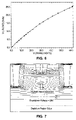
- FIG. 5 is a graph of the drain current vs. drain voltage for the simulated device of FIG. 2 , showing a breakdown at around 60 volts.
- FIG. 6 is a graph of the floating trench voltage vs. drain voltage for the simulated device of FIG. 2 , illustrating a coupling ratio of approximately 2/5.
- FIG. 7 illustrates an embodiment where breakdown occurs near the middle of the drift region rather than near a dielectric surface.
- the oxide liner is much thicker than required in order to contrast the technique with an Oxide Bypassed technique.
- FIG. 8 illustrates a computer simulation of an Oxide Bypassed technique with the trenches tied to the source/body voltage (0 volts), but with other parameters identical to that of FIG. 7 , to show the increased breakdown voltage of the invention of FIG. 7 compared to the Oxide Bypassed technique.
- FIG. 9 illustrates how multiple DMOS transistors in parallel may be located between the floating trenches.
- FIG. 10 is a top down view of a substrate illustrating multiple floating trenches within an array of DMOS transistors, similar to the transistors of FIG. 9 , for increasing the breakdown voltage.
- FIG. 11 is a top down view of a substrate illustrating multiple floating trenches within an array of DMOS transistors, where the transistors are rotated 90 degrees compared to the transistors of FIG. 10 , for increasing the breakdown voltage.
- FIG. 12 is a top down view of a cellular layout using rectangular cells with a floating trench surrounding a plurality of the cells.
- FIG. 13 is a top down view of a cellular layout using hexagonal cells with a floating trench surrounding a plurality of the cells.
- FIG. 14 is a top down view of a cellular layout using octagonal cells with a floating trench surrounding a plurality of the cells.
- FIG. 15 is a top down view of a cellular layout using circular cells with a floating trench surrounding a plurality of the cells.
- Breakdown typically occurs in a vertical DMOS where the electric field lines in the drift region bunch up so as to create a high potential difference over a relatively small portion of silicon.
- Increasing the breakdown voltage has been achieved by avoiding sharp corners in junctions and by other techniques.
- the present invention further shapes the field lines in the drift region by using opposing floating trenches, where the potential on the floating trenches depletes the drift region and shapes the field lines to increase the breakdown voltage.
- FIG. 1 shows the floating trench technique being applied to both a VDMOS transistor 10 , with a gate overlying the substrate surface, and a TDMOS transistor 12 , with a vertical gate formed in a trench.
- a VDMOS transistor 10 with a gate overlying the substrate surface
- a TDMOS transistor 12 with a vertical gate formed in a trench.
- the DMOS transistors are N-channel types, although the devices can also be formed as P-channel devices where all conductivities are reversed.
- the starting silicon substrate is an N+ type.
- the bottom surface of the substrate forms an N+ drain contact 20 .
- the N+ drain may also be a buried layer with N+ sinkers connecting the buried layer to top surface drain contacts.
- An N ⁇ epitaxial layer 22 is grown to a desired thickness, depending on the intended operating voltage of the device.
- the epitaxial layer 22 acts as a drift region.
- the substrate may be a lightly doped N-type so that an epitaxial layer need not be grown.
- Trenches are then formed in the silicon surface. Deep trenches 24 , 25 , and 26 are formed for the floating trenches. More shallow trenches 28 are formed for the TDMOS transistors. The trenches are oxidized to form a layer of insulating oxide 30 - 33 on the walls of the trenches to insulate the subsequently deposited polysilicon from the N-epi 22 . The depth of the trenches 24 - 26 affect the coupling ratio of the floating trenches to the drain voltage and the extent of depletion of the drift region, as will be described later. The optimum physical characteristics of the floating trenches depend on the requirements of the particular DMOS transistor.
- the trenches 24 - 26 and 28 are filled with polysilicon 36 - 39 , respectively.
- the poly 39 for the gate will be highly doped to create a highly conductive gate that is electrically connected (not shown).
- the poly 36 - 38 for the deep trenches 24 - 26 may be doped or undoped.
- the poly 36 - 38 is insulated from all regions of the DMOS transistor and is thus floating. Since there is no current flowing in the floating poly, there is minimal impact on performance if the poly is doped or undoped.
- a very thin gate oxide 40 is formed on the top surface, and a conductive gate 42 , such as doped poly, is deposited.
- P-type body regions 44 and 45 are formed using the gates to self-align the body regions.
- P+ body contact regions 48 and 49 are formed to achieve ohmic contact to the body regions.
- a portion of the body regions 44 and 45 next to the gate forms a channel region.
- N+ source regions 50 and 51 are formed in the body region.
- a threshold voltage applied to the gate 42 or gate/poly 39 will invert the body region next to the gate to create a conductive N-channel through the body region to cause current to be conducted between the sources and the drain. All aspects of forming the transistors, except for the floating trenches, are well known and need not be described in detail.
- the floating trenches 24 - 26 are capacitively coupled to the N-epi 22 (drift region) and body region 44 or 45 .
- the body region is typically biased at 0 volts, and the drain is typically biased at a positive power supply voltage (e.g., 60 volts). Therefore, the floating trenches will assume a potential somewhere between the body voltage and the drain voltage. In one embodiment, the floating trenches will be at a voltage approximately mid-way between the body and drain voltages. Since the floating trenches are at a voltage lower than the N-epi 22 voltage, the floating trenches will deplete the area of the N-epi 22 between the opposing floating trenches and change the electric field lines, as will be described with respect to FIG. 3 .
- drift epi resistivity determines not only the specific on-resistance of the device, but also the breakdown voltage, since the epi resistivity affects the capacitive coupling between the drift region and the P-type body to the floating poly.
- the potential on the floating trench with respect to the drift region sets the depletion width in the drift region, which is a function of the degree of field shaping.
- the P-body region 44 is relatively shallow. This shallow P-type junction may pose some difficulty for establishing adequate coupling to the floating trenches, leading to too high of a potential on the floating trenches, much closer to the drain voltage. This will defeat the field shaping effect where not enough depletion is imposed in the drift region.
- This problem can be overcome with the aid of source/p-body metal 54 , shown in FIG. 1 .
- the total dielectric 56 thickness between the source/p-body metal 54 and the floating trenches would be the primary parameter in determining the coupling ratio.
- the TDMOS transistor 12 can also benefit from the source/p-body metal 54 .
- Source/p-body metal 54 For devices operating in voltage range between 60-100V, ⁇ 30% of on-resistance is contributed to channel resistance, and the remaining ⁇ 70% to resistance in the drift region.
- Source metal improves coupling of the floating trench to the lowest potential in the device. This allows doping in the P-body region to be low and just sufficiently doped to suppress source-drain punch through leakage, which reduces channel resistance in the on-state.
- FIG. 2 is a cross-section of a TDMOS transistor similar to transistor 12 in FIG. 1 , and similar components are identified with the same numerals.
- the device of FIG. 2 was used to simulate the effect of the floating trenches.
- the N+ substrate portion begins at the bottom of FIG. 2 .
- the dimensions of the transistor in FIG. 2 are to scale.
- the trench spacing is about 1.5 microns, and the trenches are about 2.5 microns deep.
- the size and spacing of the trenches depend on the layout of the transistor, the voltage rating of the transistor, and the thickness of the epi layer.
- the epi layer in FIG. 2 is about 3 microns thick.
- the required trench oxide thickness depends on the voltage difference between the trench poly and the drift region or body region.
- FIG. 3 shows the electric field lines 60 with a drain voltage of around 60 volts.
- the depletion regions created by the floating trenches 37 and 38 increase laterally toward the middle of the drift region (epi 22 ) as the drain voltage is increased until the depletion regions merged (pinch off) and continued to expand vertically. Ultimately, the drift region between the opposing trenches is fully depleted.
- the depletion region edge 61 is labeled at the bottom of the drift region of FIG. 3 .
- the fundamental breakdown limitation near a junction is due to the nature of the junction curvature that results in a convex shape of field lines at the junction edge.
- This convex curvature causes field lines to bunch or concentrate at a region, imposing a limit in breakdown voltage.
- the depletion regions from two opposing trenches will first merge laterally, and then continue to expand in the vertical direction.
- the n-epi drift region is completed depleted or pinched, and the resultant field lines within drift region become concave instead of convex, as shown in areas 62 in FIG. 3 , to increase device breakdown voltage.
- the field lines are curved around the top of the floating trenches at areas 64 to additionally reduce crowding of the field lines.
- FIG. 5 is a graph of drain current (Id) vs. drain voltage, showing that breakdown occurs at slightly higher than 60 volts.
- FIG. 6 is a graph of the floating poly voltage (Vfloat) vs. drain voltage, showing a coupling ratio of about 2/5.
- breakdown can be forced to occur in the middle of the drift region, at a depth deeper than the floating trench depth, as shown in FIG. 7 .
- This bulk breakdown characteristic further ensures device ruggedness by moving breakdown away from a dielectric surface that may cause breakdown walking and/or possible injection of hot carriers into the floating poly, perturbing the field shaping effect.
- the enhanced performance for the Floating Trench Technique can be further illustrated by comparing it with the Oxide-Bypassed technique, where the field-shaping poly is physically and electrically connected by metal to the source/P-type body metal as shown in FIG. 8 .
- the design of FIG. 8 was created by the present inventor for the comparison, although the coupling of poly-filled trenches to a fixed voltage is prior art.
- the devices of FIGS. 7 and 8 have identical device parameters including oxide thickness (in the present example the oxide thickness used for the floating trench is much higher than required), epi thickness/resistivity, and trench/trench spacing, etc.
- Breakdown voltage for the floating trench technique is ⁇ 15V higher than that using the Oxide-Bypassed method, with the Oxide-Bypassed breakdown limited by the dielectric thickness in the field-shaping region.
- the dielectric thickness in the Oxide-Bypassed trench has to be thick enough to sustain a full-scale voltage drop between source and drain in the blocking state, where the dielectric thickness of the floating technique need only sustain the difference between the floating poly potential and drain bias.
- Equivalent breakdown for an Oxide-Bypassed device can be achieved by thickening both sidewall and bottom trench dielectric, but at the expense of increasing cell pitch and thus increasing specific on-resistance.
- the specific on-resistance can be further reduced by integrating more than one TDMOS transistor between the floating field-shaping trenches as depicted in FIG. 9 .
- the structure of FIG. 9 may only be a small portion of a power DMOS device.
- One important design parameter is the spacing between the trenches 25 and 26 . Too wide a spacing will lead to insufficient field shaping effect, resulting in incomplete depletion between the floating trenches in the drift region, causing lower breakdown to occur. Optimizing drift-epi resistivity and thickness is important to achieve high breakdown voltage.
- FIG. 10 is a top down view of a portion of a power device using the structure of FIG. 9 , where many TDMOS transistors in a two-dimensional array are connected in parallel. Only four transistors are shown for simplicity. There may be more than one hundred individual transistors in an array.
- the poly in all the deep trenches 25 , 26 , and 70 may be connected together by a poly connector 74 . Alternatively, the poly is not connected together. Each pair of trenches opposes a number of TDMOS transistors. More than two transistors may be opposed by a pair of floating trenches.
- the floating trenches completely surround the perimeter of the array (occurring out of the view of FIG. 10 ). In other words, a floating trench similar to trench 74 would connect together the right ends of trenches 25 , 26 , and 70 .
- the TDMOS transistor sources, bodies, and gates in FIG. 10 are shown extending horizontally along the horizontal trenches.
- the width dimensions of the gates are parallel to the floating trenches.
- the sources 76 , bodies 77 , and gates 78 extend vertically along the horizontal trenches.
- the width dimensions of the gates are perpendicular to the floating trenches. There may be any number of floating trenches and transistors in the array, and the floating trenches completely encircle the transistors, as in FIG. 10 .
- An outer poly-filled trench may surround the entire structure to reduce field crowding due to edge effects.
- the parasitic N-channel MOSFET comprises the intrinsic N+ source region, bottom drain electrode, and floating trench poly gate.
- a more positive potential on the floating poly with respect to the source/P-body will cause depletion in the P-type diffused body, and when inversion occurs at a higher bias, a conducting channel is formed along the trench sidewall, causing leakage current in the off-state.
- This problem can be eliminated by the absence of a source region on both sides of the field-shaping region, where a body region surrounds the active region.
- FIG. 12 illustrates a portion of a cellular layout of DMOS transistors surrounded by floating trenches 80 .
- the cells are rectangular.
- the floating trench portion enclosing the right side of the array is not shown.
- Shown are source regions 82 , P-body regions 84 , and gates 86 .
- the gates 86 shown are in trenches (like in the trench MOSFET of FIGS. 1 and 2 ), the gates may also be formed over the surface of the substrate, as shown by the VMOS of FIG. 1 .
- a floating trench surrounds each individual transistor.
- FIG. 13 illustrates a portion of a cellular layout of DMOS transistors surrounded by floating trenches 90 .
- the cells are hexagonal. Each cell is surrounded by a floating trench. Shown are source regions 92 , P-body regions 94 , and gates 96 .
- the gates 96 may be in trenches or over the surface of the substrate, as shown in FIG. 1 .
- FIG. 14 illustrates a portion of a cellular layout of DMOS transistors surrounded by floating trenches 100 .
- the cells are octagonal. Each cell is surrounded by a floating trench. Shown are source regions 102 , P-body regions 104 , and gates 106 .
- the gates 106 may be in trenches or over the surface of the substrate, as shown in FIG. 1 .
- FIG. 15 illustrates a portion of a cellular layout of DMOS transistors surrounded by floating trenches 110 .
- the cells are circular.
- the cells may also be oval.
- Each cell is surrounded by a floating trench.
- Shown are source regions 112 , P-body regions 114 , and gates 116 .
- the gates 116 may be in trenches or over the surface of the substrate, as shown in FIG. 1 .
- the floating trenches surrounding the cells are opposing trench portions that create a depletion region in the drift region that extends laterally and merges under the gate to increase the breakdown voltage.
- Each opposing portion of a continuous trench (such as opposing sides of a hexagonal trench) is considered to be an opposing trench portion for purposes of the present description.
- opposing sides of the circular trench are considered to be opposing trench portions. It is understood that the geometric patterns describe may not be perfect geometrical shapes when actually fabricated, but may be substantially similar to the intended geometric shape.
- the preferred embodiment substantially totally depletes the drift region below the gate at near the maximum voltage rating of the transistor, increased breakdown is achieved by even small amounts of depletion under the gate as long as the lateral depletion regions are merged.
- the high depletion levels described may be those existing at slightly below the maximum voltage rating (i.e., breakdown voltage rating) of the transistors.
Abstract
Description
Claims (30)
Priority Applications (1)
| Application Number | Priority Date | Filing Date | Title |
|---|---|---|---|
| US11/351,644 US7514743B2 (en) | 2005-08-23 | 2006-02-09 | DMOS transistor with floating poly-filled trench for improved performance through 3-D field shaping |
Applications Claiming Priority (3)
| Application Number | Priority Date | Filing Date | Title |
|---|---|---|---|
| US71105005P | 2005-08-23 | 2005-08-23 | |
| US11/234,519 US7535057B2 (en) | 2005-05-24 | 2005-09-23 | DMOS transistor with a poly-filled deep trench for improved performance |
| US11/351,644 US7514743B2 (en) | 2005-08-23 | 2006-02-09 | DMOS transistor with floating poly-filled trench for improved performance through 3-D field shaping |
Related Parent Applications (1)
| Application Number | Title | Priority Date | Filing Date |
|---|---|---|---|
| US11/234,519 Continuation-In-Part US7535057B2 (en) | 2005-05-24 | 2005-09-23 | DMOS transistor with a poly-filled deep trench for improved performance |
Publications (2)
| Publication Number | Publication Date |
|---|---|
| US20070052060A1 US20070052060A1 (en) | 2007-03-08 |
| US7514743B2 true US7514743B2 (en) | 2009-04-07 |
Family
ID=37829284
Family Applications (1)
| Application Number | Title | Priority Date | Filing Date |
|---|---|---|---|
| US11/351,644 Expired - Fee Related US7514743B2 (en) | 2005-08-23 | 2006-02-09 | DMOS transistor with floating poly-filled trench for improved performance through 3-D field shaping |
Country Status (1)
| Country | Link |
|---|---|
| US (1) | US7514743B2 (en) |
Cited By (11)
| Publication number | Priority date | Publication date | Assignee | Title |
|---|---|---|---|---|
| US20080303085A1 (en) * | 2007-06-07 | 2008-12-11 | Samsung Electronics Co., Ltd. | Semiconductor device including active pattern with channel recess, and method of fabricating the same |
| US20100013009A1 (en) * | 2007-12-14 | 2010-01-21 | James Pan | Structure and Method for Forming Trench Gate Transistors with Low Gate Resistance |
| US20100013552A1 (en) * | 2008-07-15 | 2010-01-21 | Maxpower Semiconductor Inc. | MOSFET Switch with Embedded Electrostatic Charge |
| CN102184857A (en) * | 2011-03-29 | 2011-09-14 | 上海宏力半导体制造有限公司 | Method for preparing trench field effect tube |
| US20130153926A1 (en) * | 2011-12-20 | 2013-06-20 | Sumitomo Electric Industries, Ltd. | Semiconductor device and method for manufacturing same |
| US8530961B2 (en) | 2009-10-28 | 2013-09-10 | Csmc Technologies Fab1 Co., Ltd. | Compatible vertical double diffused metal oxide semiconductor transistor and lateral double diffused metal oxide semiconductor transistor and manufacture method thereof |
| US8853774B2 (en) * | 2012-11-30 | 2014-10-07 | Infineon Technologies Ag | Semiconductor device including trenches and method of manufacturing a semiconductor device |
| US9099553B2 (en) | 2012-01-13 | 2015-08-04 | Sumitomo Electric Industries, Ltd. | Semiconductor device and method for manufacturing same |
| US20160204210A1 (en) * | 2015-01-13 | 2016-07-14 | Infineon Technologies Austria Ag | Semiconductor Device Having Field Plate Structures and Gate Electrode Structures Between the Field Plate Structures |
| US20170069752A1 (en) * | 2015-09-07 | 2017-03-09 | Kabushiki Kaisha Toshiba | Semiconductor device |
| US9660021B1 (en) * | 2013-10-03 | 2017-05-23 | Texas Instruments Incorporated | Trench gate trench field plate vertical MOSFET |
Families Citing this family (13)
| Publication number | Priority date | Publication date | Assignee | Title |
|---|---|---|---|---|
| US8080848B2 (en) * | 2006-05-11 | 2011-12-20 | Fairchild Semiconductor Corporation | High voltage semiconductor device with lateral series capacitive structure |
| US20080296636A1 (en) * | 2007-05-31 | 2008-12-04 | Darwish Mohamed N | Devices and integrated circuits including lateral floating capacitively coupled structures |
| TWI357108B (en) * | 2007-08-21 | 2012-01-21 | Nat Univ Tsing Hua | Semiconductor device structure |
| US8193565B2 (en) | 2008-04-18 | 2012-06-05 | Fairchild Semiconductor Corporation | Multi-level lateral floating coupled capacitor transistor structures |
| US8624302B2 (en) * | 2010-02-05 | 2014-01-07 | Fairchild Semiconductor Corporation | Structure and method for post oxidation silicon trench bottom shaping |
| US8901676B2 (en) * | 2011-01-03 | 2014-12-02 | International Business Machines Corporation | Lateral extended drain metal oxide semiconductor field effect transistor (LEDMOSFET) having a high drain-to-body breakdown voltage (Vb), a method of forming an LEDMOSFET, and a silicon-controlled rectifier (SCR) incorporating a complementary pair of LEDMOSFETs |
| US8659079B2 (en) * | 2012-05-29 | 2014-02-25 | Nanya Technology Corporation | Transistor device and method for manufacturing the same |
| US9245960B2 (en) | 2013-02-08 | 2016-01-26 | Globalfoundries Inc. | Lateral extended drain metal oxide semiconductor field effect transistor (LEDMOSFET) with tapered airgap field plates |
| CN104518021A (en) * | 2013-09-26 | 2015-04-15 | 无锡华润华晶微电子有限公司 | VDMOS device cellular structure and manufacture method thereof |
| DE102015105758A1 (en) * | 2015-04-15 | 2016-10-20 | Infineon Technologies Ag | SEMICONDUCTOR COMPONENT AND MANUFACTURING METHOD |
| CN106098781B (en) * | 2016-08-17 | 2018-10-26 | 电子科技大学 | A kind of VDMOS of groove structure |
| CN106298937B (en) * | 2016-08-17 | 2019-02-01 | 电子科技大学 | A kind of groove-shaped VDMOS |
| CN108054211A (en) * | 2017-12-21 | 2018-05-18 | 深圳市晶特智造科技有限公司 | Trench vertical bilateral diffusion metal oxide transistor and preparation method thereof |
Citations (14)
| Publication number | Priority date | Publication date | Assignee | Title |
|---|---|---|---|---|
| US5204545A (en) | 1989-11-22 | 1993-04-20 | Mitsubishi Denki Kabushiki Kaisha | Structure for preventing field concentration in semiconductor device and method of forming the same |
| US5233215A (en) | 1992-06-08 | 1993-08-03 | North Carolina State University At Raleigh | Silicon carbide power MOSFET with floating field ring and floating field plate |
| US6246101B1 (en) | 1998-07-07 | 2001-06-12 | Mitsubishi Denki Kabushiki Kaisha | Isolation structure and semiconductor device including the isolation structure |
| US6362505B1 (en) * | 1998-11-27 | 2002-03-26 | Siemens Aktiengesellschaft | MOS field-effect transistor with auxiliary electrode |
| US6410958B1 (en) * | 2000-11-27 | 2002-06-25 | Kabushiki Kaisha Toshiba | Power MOSFET having laterally three-layered structure formed among element isolation regions |
| US6452230B1 (en) | 1998-12-23 | 2002-09-17 | International Rectifier Corporation | High voltage mosgated device with trenches to reduce on-resistance |
| US6608350B2 (en) | 2000-12-07 | 2003-08-19 | International Rectifier Corporation | High voltage vertical conduction superjunction semiconductor device |
| US6710403B2 (en) * | 2002-07-30 | 2004-03-23 | Fairchild Semiconductor Corporation | Dual trench power MOSFET |
| US6774734B2 (en) | 2002-11-27 | 2004-08-10 | International Business Machines Corporation | Ring oscillator circuit for EDRAM/DRAM performance monitoring |
| US6774434B2 (en) | 2001-11-16 | 2004-08-10 | Koninklijke Philips Electronics N.V. | Field effect device having a drift region and field shaping region used as capacitor dielectric |
| US6803626B2 (en) | 2002-07-18 | 2004-10-12 | Fairchild Semiconductor Corporation | Vertical charge control semiconductor device |
| US20050156232A1 (en) | 2001-09-13 | 2005-07-21 | Hueting Raymond J. | Edge termination in MOS transistors |
| US6991977B2 (en) | 2001-10-17 | 2006-01-31 | Fairchild Semiconductor Corporation | Method for forming a semiconductor structure with improved smaller forward voltage loss and higher blocking capability |
| US7126187B2 (en) * | 2002-08-22 | 2006-10-24 | Denso Corporation | Semiconductor device and a method of producing the same |
-
2006
- 2006-02-09 US US11/351,644 patent/US7514743B2/en not_active Expired - Fee Related
Patent Citations (15)
| Publication number | Priority date | Publication date | Assignee | Title |
|---|---|---|---|---|
| US5204545A (en) | 1989-11-22 | 1993-04-20 | Mitsubishi Denki Kabushiki Kaisha | Structure for preventing field concentration in semiconductor device and method of forming the same |
| US5334546A (en) | 1989-11-22 | 1994-08-02 | Mitsubishi Denki Kabushiki Kaisha | Method of forming a semiconductor device which prevents field concentration |
| US5233215A (en) | 1992-06-08 | 1993-08-03 | North Carolina State University At Raleigh | Silicon carbide power MOSFET with floating field ring and floating field plate |
| US6246101B1 (en) | 1998-07-07 | 2001-06-12 | Mitsubishi Denki Kabushiki Kaisha | Isolation structure and semiconductor device including the isolation structure |
| US6362505B1 (en) * | 1998-11-27 | 2002-03-26 | Siemens Aktiengesellschaft | MOS field-effect transistor with auxiliary electrode |
| US6452230B1 (en) | 1998-12-23 | 2002-09-17 | International Rectifier Corporation | High voltage mosgated device with trenches to reduce on-resistance |
| US6410958B1 (en) * | 2000-11-27 | 2002-06-25 | Kabushiki Kaisha Toshiba | Power MOSFET having laterally three-layered structure formed among element isolation regions |
| US6608350B2 (en) | 2000-12-07 | 2003-08-19 | International Rectifier Corporation | High voltage vertical conduction superjunction semiconductor device |
| US20050156232A1 (en) | 2001-09-13 | 2005-07-21 | Hueting Raymond J. | Edge termination in MOS transistors |
| US6991977B2 (en) | 2001-10-17 | 2006-01-31 | Fairchild Semiconductor Corporation | Method for forming a semiconductor structure with improved smaller forward voltage loss and higher blocking capability |
| US6774434B2 (en) | 2001-11-16 | 2004-08-10 | Koninklijke Philips Electronics N.V. | Field effect device having a drift region and field shaping region used as capacitor dielectric |
| US6803626B2 (en) | 2002-07-18 | 2004-10-12 | Fairchild Semiconductor Corporation | Vertical charge control semiconductor device |
| US6710403B2 (en) * | 2002-07-30 | 2004-03-23 | Fairchild Semiconductor Corporation | Dual trench power MOSFET |
| US7126187B2 (en) * | 2002-08-22 | 2006-10-24 | Denso Corporation | Semiconductor device and a method of producing the same |
| US6774734B2 (en) | 2002-11-27 | 2004-08-10 | International Business Machines Corporation | Ring oscillator circuit for EDRAM/DRAM performance monitoring |
Non-Patent Citations (8)
| Title |
|---|
| Andy Strachan et al., "A Trench-Isolated Power BiCMOS Process with Complimentary High Performance Vertical Bipolars," paper, Advanced Process Technology Development, National Semiconductor, Santa Clara, CA, 4 pages. |
| B. Elattari et al., "Impact of Charging on Breakdown in Deep Trench Isolation Structures", European Solid-State Device Research, 2003, pp. 513-516. |
| Hidefumi Takaya et al., Floating Island and Thick Bottom Oxide Trench Gate MOSFET (FITMOS), Proceedings of the 17th International Symposium on Power Semiconductor Devices & IC's, May 23-26, 2005, Santa Barbara, CA pp. 43-46. |
| R.Van Dalen et al., "Breaking the Silicon limit using semi-insulating Resurf layers," Proceedings of 2001 International Symposium on Power Semiconductor Devices & IC's, Osaka, pp. 391-394. |
| V. Parthasarathy et al., "A 0.25mum CMOS based 70V smart power technology with deep trench for high-voltage isolation," 2002 IEEE, pp. 459-462. |
| Xin Yang et al., "Tunable Oxide-Bypassed Trench Gate MOSFET: Breaking the Ideal Superjunction MOSFET Performance Line at Equal Column Width," IEEE Electron Device Letters, vol. 24, No. 11, Nov. 2003, pp. 704-706. |
| Yung C. Liang et al., "Oxide-Bypassed VDMOS (OBVDMOS): An alternative to Superjunction High Voltage MOS Power Devices," IEEE Electron Devices Letters, vol. 22, No. 8, Aug. 2001, pp. 407-409. |
| Yung C. Liang et al., "Tunable Oxide-Bypassed VDMOS (OBVDMOS): Breaking the Silicon Limit for the Second Generaton," 2002 IEEE, pp. 201-204. |
Cited By (21)
| Publication number | Priority date | Publication date | Assignee | Title |
|---|---|---|---|---|
| US20080303085A1 (en) * | 2007-06-07 | 2008-12-11 | Samsung Electronics Co., Ltd. | Semiconductor device including active pattern with channel recess, and method of fabricating the same |
| US7667266B2 (en) * | 2007-06-07 | 2010-02-23 | Samsung Electronics Co., Ltd. | Semiconductor device including active pattern with channel recess, and method of fabricating the same |
| US20100013009A1 (en) * | 2007-12-14 | 2010-01-21 | James Pan | Structure and Method for Forming Trench Gate Transistors with Low Gate Resistance |
| US20100013552A1 (en) * | 2008-07-15 | 2010-01-21 | Maxpower Semiconductor Inc. | MOSFET Switch with Embedded Electrostatic Charge |
| US8310001B2 (en) * | 2008-07-15 | 2012-11-13 | Maxpower Semiconductor Inc. | MOSFET switch with embedded electrostatic charge |
| US8530961B2 (en) | 2009-10-28 | 2013-09-10 | Csmc Technologies Fab1 Co., Ltd. | Compatible vertical double diffused metal oxide semiconductor transistor and lateral double diffused metal oxide semiconductor transistor and manufacture method thereof |
| CN102184857A (en) * | 2011-03-29 | 2011-09-14 | 上海宏力半导体制造有限公司 | Method for preparing trench field effect tube |
| US20130153926A1 (en) * | 2011-12-20 | 2013-06-20 | Sumitomo Electric Industries, Ltd. | Semiconductor device and method for manufacturing same |
| US8829605B2 (en) * | 2011-12-20 | 2014-09-09 | Sumitomo Electric Industries, Ltd. | Semiconductor device having deep and shallow trenches |
| US9099553B2 (en) | 2012-01-13 | 2015-08-04 | Sumitomo Electric Industries, Ltd. | Semiconductor device and method for manufacturing same |
| US8853774B2 (en) * | 2012-11-30 | 2014-10-07 | Infineon Technologies Ag | Semiconductor device including trenches and method of manufacturing a semiconductor device |
| DE102013112608B4 (en) | 2012-11-30 | 2019-09-26 | Infineon Technologies Ag | Semiconductor device with trenches and method for producing a semiconductor device |
| US9660021B1 (en) * | 2013-10-03 | 2017-05-23 | Texas Instruments Incorporated | Trench gate trench field plate vertical MOSFET |
| US10062777B2 (en) | 2013-10-03 | 2018-08-28 | Texas Instruments Incorporated | Trench gate trench field plate vertical MOSFET |
| US10811530B2 (en) | 2013-10-03 | 2020-10-20 | Texas Instruments Incorporated | Trench gate trench field plate vertical mosfet |
| US11189721B2 (en) | 2013-10-03 | 2021-11-30 | Texas Instruments Incorporated | Trench gate trench field plate vertical MOSFET |
| US20160204210A1 (en) * | 2015-01-13 | 2016-07-14 | Infineon Technologies Austria Ag | Semiconductor Device Having Field Plate Structures and Gate Electrode Structures Between the Field Plate Structures |
| US9691862B2 (en) * | 2015-01-13 | 2017-06-27 | Infineon Technologies Austria Ag | Semiconductor device having field plate structures and gate electrode structures between the field plate structures |
| US10068975B2 (en) | 2015-01-13 | 2018-09-04 | Infineon Technologies Austria Ag | Semiconductor device having field plate structures, source regions and gate electrode structures between the field plate structures |
| US20170069752A1 (en) * | 2015-09-07 | 2017-03-09 | Kabushiki Kaisha Toshiba | Semiconductor device |
| US9647109B2 (en) * | 2015-09-07 | 2017-05-09 | Kabushiki Kaisha Toshiba | Semiconductor device |
Also Published As
| Publication number | Publication date |
|---|---|
| US20070052060A1 (en) | 2007-03-08 |
Similar Documents
| Publication | Publication Date | Title |
|---|---|---|
| US7514743B2 (en) | DMOS transistor with floating poly-filled trench for improved performance through 3-D field shaping | |
| US9947779B2 (en) | Power MOSFET having lateral channel, vertical current path, and P-region under gate for increasing breakdown voltage | |
| US7535057B2 (en) | DMOS transistor with a poly-filled deep trench for improved performance | |
| US8310001B2 (en) | MOSFET switch with embedded electrostatic charge | |
| US8354711B2 (en) | Power MOSFET and its edge termination | |
| US9184248B2 (en) | Vertical power MOSFET having planar channel and its method of fabrication | |
| US8890280B2 (en) | Trench-type semiconductor power devices | |
| US6849880B1 (en) | Power semiconductor device | |
| TWI459562B (en) | Staggered column superjunction | |
| CN104201206B (en) | A kind of laterally SOI power LDMOS device | |
| US8330213B2 (en) | Power semiconductor devices, methods, and structures with embedded dielectric layers containing permanent charges | |
| US20070126055A1 (en) | Trench insulated gate field effect transistor | |
| US20100219468A1 (en) | Power device structures and methods | |
| US7276405B2 (en) | Power semiconductor device having high breakdown voltage, low on-resistance and small switching loss and method of forming the same | |
| US20150076593A1 (en) | Power devices, structures, components, and methods using lateral drift, fixed net charge, and shield | |
| CN105633132A (en) | Semiconductor device with charge compensation region underneath gate trench | |
| KR100381845B1 (en) | Long channel trench-gated power mosfet having fully depleted body region | |
| EP3385993B1 (en) | Lateral diffused metal oxide semiconductor field effect transistor | |
| CN111816707B (en) | Equipotential drop field device for eliminating in-vivo curvature effect and manufacturing method thereof | |
| CN107564965B (en) | Transverse double-diffusion MOS device | |
| EP3361511A1 (en) | Laterally diffused metal-oxide semiconductor field-effect transistor | |
| CN107275388B (en) | Transverse high-voltage device | |
| CN115332338B (en) | Super-junction VDMOS device for adjusting dynamic characteristics and preparation method thereof | |
| CN107546274B (en) | LDMOS device with step-shaped groove | |
| US11316021B2 (en) | High density power device with selectively shielded recessed field plate |
Legal Events
| Date | Code | Title | Description |
|---|---|---|---|
| FPAY | Fee payment |
Year of fee payment: 4 |
|
| AS | Assignment |
Owner name: U.S. BANK NATIONAL ASSOCIATION, AS COLLATERAL AGENT, CALIFORNIA Free format text: SECURITY INTEREST;ASSIGNOR:MICRON TECHNOLOGY, INC.;REEL/FRAME:038669/0001 Effective date: 20160426 Owner name: U.S. BANK NATIONAL ASSOCIATION, AS COLLATERAL AGEN Free format text: SECURITY INTEREST;ASSIGNOR:MICRON TECHNOLOGY, INC.;REEL/FRAME:038669/0001 Effective date: 20160426 |
|
| REMI | Maintenance fee reminder mailed | ||
| LAPS | Lapse for failure to pay maintenance fees | ||
| STCH | Information on status: patent discontinuation |
Free format text: PATENT EXPIRED DUE TO NONPAYMENT OF MAINTENANCE FEES UNDER 37 CFR 1.362 |
|
| FP | Expired due to failure to pay maintenance fee |
Effective date: 20170407 |
|
| AS | Assignment |
Owner name: U.S. BANK NATIONAL ASSOCIATION, AS COLLATERAL AGENT, CALIFORNIA Free format text: CORRECTIVE ASSIGNMENT TO CORRECT THE REPLACE ERRONEOUSLY FILED PATENT #7358718 WITH THE CORRECT PATENT #7358178 PREVIOUSLY RECORDED ON REEL 038669 FRAME 0001. ASSIGNOR(S) HEREBY CONFIRMS THE SECURITY INTEREST;ASSIGNOR:MICRON TECHNOLOGY, INC.;REEL/FRAME:043079/0001 Effective date: 20160426 Owner name: U.S. BANK NATIONAL ASSOCIATION, AS COLLATERAL AGEN Free format text: CORRECTIVE ASSIGNMENT TO CORRECT THE REPLACE ERRONEOUSLY FILED PATENT #7358718 WITH THE CORRECT PATENT #7358178 PREVIOUSLY RECORDED ON REEL 038669 FRAME 0001. ASSIGNOR(S) HEREBY CONFIRMS THE SECURITY INTEREST;ASSIGNOR:MICRON TECHNOLOGY, INC.;REEL/FRAME:043079/0001 Effective date: 20160426 |