US7518493B2 - Integrated tire pressure sensor system - Google Patents
Integrated tire pressure sensor system Download PDFInfo
- Publication number
- US7518493B2 US7518493B2 US11/292,946 US29294605A US7518493B2 US 7518493 B2 US7518493 B2 US 7518493B2 US 29294605 A US29294605 A US 29294605A US 7518493 B2 US7518493 B2 US 7518493B2
- Authority
- US
- United States
- Prior art keywords
- mems
- pressure sensor
- sensor
- set forth
- tire pressure
- Prior art date
- Legal status (The legal status is an assumption and is not a legal conclusion. Google has not performed a legal analysis and makes no representation as to the accuracy of the status listed.)
- Active, expires
Links
Images


Classifications
-
- B—PERFORMING OPERATIONS; TRANSPORTING
- B60—VEHICLES IN GENERAL
- B60C—VEHICLE TYRES; TYRE INFLATION; TYRE CHANGING; CONNECTING VALVES TO INFLATABLE ELASTIC BODIES IN GENERAL; DEVICES OR ARRANGEMENTS RELATED TO TYRES
- B60C23/00—Devices for measuring, signalling, controlling, or distributing tyre pressure or temperature, specially adapted for mounting on vehicles; Arrangement of tyre inflating devices on vehicles, e.g. of pumps or of tanks; Tyre cooling arrangements
- B60C23/02—Signalling devices actuated by tyre pressure
- B60C23/04—Signalling devices actuated by tyre pressure mounted on the wheel or tyre
- B60C23/0408—Signalling devices actuated by tyre pressure mounted on the wheel or tyre transmitting the signals by non-mechanical means from the wheel or tyre to a vehicle body mounted receiver
-
- B—PERFORMING OPERATIONS; TRANSPORTING
- B81—MICROSTRUCTURAL TECHNOLOGY
- B81B—MICROSTRUCTURAL DEVICES OR SYSTEMS, e.g. MICROMECHANICAL DEVICES
- B81B3/00—Devices comprising flexible or deformable elements, e.g. comprising elastic tongues or membranes
- B81B3/0064—Constitution or structural means for improving or controlling the physical properties of a device
- B81B3/0086—Electrical characteristics, e.g. reducing driving voltage, improving resistance to peak voltage
-
- B—PERFORMING OPERATIONS; TRANSPORTING
- B81—MICROSTRUCTURAL TECHNOLOGY
- B81B—MICROSTRUCTURAL DEVICES OR SYSTEMS, e.g. MICROMECHANICAL DEVICES
- B81B2201/00—Specific applications of microelectromechanical systems
- B81B2201/02—Sensors
- B81B2201/0228—Inertial sensors
- B81B2201/0235—Accelerometers
-
- B—PERFORMING OPERATIONS; TRANSPORTING
- B81—MICROSTRUCTURAL TECHNOLOGY
- B81B—MICROSTRUCTURAL DEVICES OR SYSTEMS, e.g. MICROMECHANICAL DEVICES
- B81B2201/00—Specific applications of microelectromechanical systems
- B81B2201/02—Sensors
- B81B2201/0264—Pressure sensors
-
- B—PERFORMING OPERATIONS; TRANSPORTING
- B81—MICROSTRUCTURAL TECHNOLOGY
- B81B—MICROSTRUCTURAL DEVICES OR SYSTEMS, e.g. MICROMECHANICAL DEVICES
- B81B2207/00—Microstructural systems or auxiliary parts thereof
- B81B2207/01—Microstructural systems or auxiliary parts thereof comprising a micromechanical device connected to control or processing electronics, i.e. Smart-MEMS
- B81B2207/015—Microstructural systems or auxiliary parts thereof comprising a micromechanical device connected to control or processing electronics, i.e. Smart-MEMS the micromechanical device and the control or processing electronics being integrated on the same substrate
-
- B—PERFORMING OPERATIONS; TRANSPORTING
- B81—MICROSTRUCTURAL TECHNOLOGY
- B81C—PROCESSES OR APPARATUS SPECIALLY ADAPTED FOR THE MANUFACTURE OR TREATMENT OF MICROSTRUCTURAL DEVICES OR SYSTEMS
- B81C2203/00—Forming microstructural systems
- B81C2203/01—Packaging MEMS
- B81C2203/0118—Bonding a wafer on the substrate, i.e. where the cap consists of another wafer
Definitions
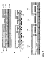
- FIG. 1 shows an example of a tire pressure sensor system integrated onto one chip according to the present invention.
- the tire pressure system is integrated onto two chips.
- all of the MEMS-based components are integrated onto a first chip, and all of the CMOS-based components are integrated onto a second chip.
- sensors 210 including MEMS-based reference capacitor 212 , MEMS-based pressure sensor 214 , MEMS-based motion sensor 216 and MEMS-oscillator-based resonator 218 are co-fabricated onto one monolithic MEMS chip 220 .
- the voltage sensor is preferably an IC-based sensor.
- the voltage sensor is also preferably a dual range, 8-bit sensor that can sense a first voltage range from about 1.2 to about 4.0 V and a second voltage range that covers voltages up to about 15V.
- the resolution of the sensor is preferably about 10 mV/lsb on the lower range and the accuracy of the sensor is preferably about ⁇ 50 mV.
- the voltage sensor preferably includes a low battery detector that powers down the system when the battery voltage at the sensor is in the range of about 1.6 to about 2.2 V.
- the voltage sensor may also detect when the battery is discharged or cold, when it has a high internal resistance preventing transmission. In this case a supporting capacitor may be charged to assist with the transmission. This helps to prolong the usable battery life.
- the calibration constants used by the signal processor are preferably stored in more than one memory location, e.g. electronically erasable programmable read-only memory (EEPROM) or FLASH, to provide an option for cross-checking potential memory corruption.
- EEPROM electronically erasable programmable read-only memory
- FLASH FLASH
- the module is “woken” by an operator using an LF signal when the tire is put into use. At this time the module goes into operating mode and may power up the microcontroller and RF sections of the ASIC, including the fractional-N synthesizer and the MEMS-oscillator-based resonator on the MEMS chip to send a return signal if required by the customer system. In other implementations a simple wake command is issued and no transmission is required.
- a fractional-N synthesizer allows the input frequency to be multiplied by a non-integer number so that variations in the output frequency of the resonator can be calibrated.
- This number is derived by the microcontroller using factory resonator calibration data in an approach analogous to the compensation of the pressure sensor outlined above.
- the number could be derived by solving a set of simultaneous equations to make output frequency equal to a desired value, based on measured resonator-based frequency at one or more temperatures during a calibration phase.
- Polarization voltage effects can be corrected in a like manner by taking the signal from the voltage sensor, calculating a correction in the microcontroller and feeding this data into the synthesizer.
- the next processing steps are performed on the reverse side of the cap wafer 500 ( FIG. 5D ). These steps provide features that define openings that will allow the sensors to contact the external environment, for example the opening for the pressure sensor.
- the oxide on the surface of the wafer 500 is patterned using photolithographic techniques to define openings in the wafer 500 . Deep reactive ion etching is used to etch a hole 514 through the entire wafer 500 , and then the handling wafer 520 is removed (not shown). The attachment and de-bonding of handling wafers is well established and is therefore not described in detail.
- the oxide layer is removed form the cap wafer and the surface is prepared for silicon-to-silicon fusion bonding as described previously.
- the IC circuits could be connected with the MEMS electrodes underneath oxide layer 304 by performing an etch through the silicon wafer 300 and the oxide layer 304 , for example using DRIE and oxide etch, followed by metallization in a similar manner as shown in FIG. 7B .
- the final step would be to etch the cavity 514 on the exposed face of cap wafer 500 .
Abstract
Description
where ∈ is a dielectric constant, A is the area of the electrode, K1, and K2 are sensor specific constants dependant on temperature, and P is pressure.
where the subscripts P and REF refer to the sense and reference capacitors, respectively.
Sensor Calibration
where CAL0 and CALFS are target calibrated sensor outputs at P0 and PFS, respectively.
-
- Zero output (CAL0) depends on both K1 (offset) and K2 (sensitivity) constants
- Full scale output (CALFS) depends on both constants as well.
Sensor Temperature Compensation
-
- If temperature errors are small enough, one can eliminate temperature compensation.
- If temperature errors are predictable with a sufficient accuracy, one can implement a statistical compensation, where predicted temperature errors will be compensated without temperature testing.
- If temperature errors are not predictable, sensors must be tested at different temperatures to measure temperature errors. If temperature errors are linear, two test temperatures are needed. For parabolic errors at least three test temperatures are needed, etc.
K 1p(T)=X 0 +X 1 *T
K 2p(T)=Y 0 +Y 1 *T
Specific calibration/compensation implementation depends on the circuit implementation.
Claims (32)
Priority Applications (3)
| Application Number | Priority Date | Filing Date | Title |
|---|---|---|---|
| US11/292,946 US7518493B2 (en) | 2005-12-01 | 2005-12-01 | Integrated tire pressure sensor system |
| PCT/US2006/046132 WO2007064961A2 (en) | 2005-12-01 | 2006-11-30 | Integrated tire pressure sensor system |
| US11/707,347 US7539003B2 (en) | 2005-12-01 | 2007-02-16 | Capacitive micro-electro-mechanical sensors with single crystal silicon electrodes |
Applications Claiming Priority (1)
| Application Number | Priority Date | Filing Date | Title |
|---|---|---|---|
| US11/292,946 US7518493B2 (en) | 2005-12-01 | 2005-12-01 | Integrated tire pressure sensor system |
Related Child Applications (1)
| Application Number | Title | Priority Date | Filing Date |
|---|---|---|---|
| US11/707,347 Continuation-In-Part US7539003B2 (en) | 2005-12-01 | 2007-02-16 | Capacitive micro-electro-mechanical sensors with single crystal silicon electrodes |
Publications (2)
| Publication Number | Publication Date |
|---|---|
| US20070125161A1 US20070125161A1 (en) | 2007-06-07 |
| US7518493B2 true US7518493B2 (en) | 2009-04-14 |
Family
ID=38092867
Family Applications (1)
| Application Number | Title | Priority Date | Filing Date |
|---|---|---|---|
| US11/292,946 Active 2026-11-18 US7518493B2 (en) | 2005-12-01 | 2005-12-01 | Integrated tire pressure sensor system |
Country Status (2)
| Country | Link |
|---|---|
| US (1) | US7518493B2 (en) |
| WO (1) | WO2007064961A2 (en) |
Cited By (66)
| Publication number | Priority date | Publication date | Assignee | Title |
|---|---|---|---|---|
| US20070063869A1 (en) * | 2002-10-01 | 2007-03-22 | Geoffrey Haswell | Telemetry unit |
| US20070156320A1 (en) * | 2000-09-08 | 2007-07-05 | Automotive Technologies International, Inc. | Vehicular Tire Monitoring Based on Sensed Acceleration |
| US20090083459A1 (en) * | 2007-09-21 | 2009-03-26 | Divyasimha Harish | Universal interface compatibility of a sensor |
| US20100019332A1 (en) * | 2008-07-24 | 2010-01-28 | Taylor William P | Methods and apparatus for integrated circuit having on chip capacitor with eddy current reductions |
| US20100052424A1 (en) * | 2008-08-26 | 2010-03-04 | Taylor William P | Methods and apparatus for integrated circuit having integrated energy storage device |
| US20100245114A1 (en) * | 2007-06-15 | 2010-09-30 | Board Of Regents, The University Of Texas System | Thin Flexible Sensor |
| US20100300207A1 (en) * | 2009-05-27 | 2010-12-02 | Temic Automotive Of North America, Inc. | Pressure sensor for harsh media sensing and flexible packaging |
| US20110030472A1 (en) * | 2009-05-27 | 2011-02-10 | King Abdullah University of Science ang Technology | Mems mass-spring-damper systems using an out-of-plane suspension scheme |
| US20110031565A1 (en) * | 2009-08-04 | 2011-02-10 | David Lambe Marx | Micromachined devices and fabricating the same |
| US20110133732A1 (en) * | 2009-12-03 | 2011-06-09 | Allegro Microsystems, Inc. | Methods and apparatus for enhanced frequency response of magnetic sensors |
| US20110304452A1 (en) * | 2010-06-15 | 2011-12-15 | Honda Motor Co., Ltd. | Two axis antenna for tpms sensor |
| US20110315235A1 (en) * | 2008-08-21 | 2011-12-29 | Warwick Ian Colefax | Valve device for pneumatic tyre including pressure sensor |
| US20130104653A1 (en) * | 2011-10-31 | 2013-05-02 | The Charles Stark Draper Laboratory, Inc. | Mems hemispherical resonator gyroscope |
| US20130255377A1 (en) * | 2012-04-03 | 2013-10-03 | Seiko Epson Corporation | Gyro sensor and electronic device including the same |
| US8629539B2 (en) | 2012-01-16 | 2014-01-14 | Allegro Microsystems, Llc | Methods and apparatus for magnetic sensor having non-conductive die paddle |
| US20140042876A1 (en) * | 2012-08-08 | 2014-02-13 | Infineon Technologies Ag | Remote Rotor Parameter Sensor for Electric Drives |
| WO2014043209A1 (en) * | 2012-09-11 | 2014-03-20 | University Of Washington Through Its Center For Commercialization | Sensor nodes, apparatuses, and methods for wirelessly transmitting data to a power infrastructure |
| US8700828B2 (en) | 2007-09-21 | 2014-04-15 | Loadstar Sensors, Inc. | Universal interface for one or more sensors |
| US8742964B2 (en) | 2012-04-04 | 2014-06-03 | Fairchild Semiconductor Corporation | Noise reduction method with chopping for a merged MEMS accelerometer sensor |
| US8754694B2 (en) | 2012-04-03 | 2014-06-17 | Fairchild Semiconductor Corporation | Accurate ninety-degree phase shifter |
| US8813564B2 (en) | 2010-09-18 | 2014-08-26 | Fairchild Semiconductor Corporation | MEMS multi-axis gyroscope with central suspension and gimbal structure |
| US8952832B2 (en) | 2008-01-18 | 2015-02-10 | Invensense, Inc. | Interfacing application programs and motion sensors of a device |
| US8960002B2 (en) | 2007-12-10 | 2015-02-24 | Invensense, Inc. | Vertically integrated 3-axis MEMS angular accelerometer with integrated electronics |
| US8978475B2 (en) | 2012-02-01 | 2015-03-17 | Fairchild Semiconductor Corporation | MEMS proof mass with split z-axis portions |
| US8997564B2 (en) | 2007-07-06 | 2015-04-07 | Invensense, Inc. | Integrated motion processing unit (MPU) with MEMS inertial sensing and embedded digital electronics |
| US9006846B2 (en) | 2010-09-20 | 2015-04-14 | Fairchild Semiconductor Corporation | Through silicon via with reduced shunt capacitance |
| US9062972B2 (en) | 2012-01-31 | 2015-06-23 | Fairchild Semiconductor Corporation | MEMS multi-axis accelerometer electrode structure |
| US9069006B2 (en) | 2012-04-05 | 2015-06-30 | Fairchild Semiconductor Corporation | Self test of MEMS gyroscope with ASICs integrated capacitors |
| US9095072B2 (en) | 2010-09-18 | 2015-07-28 | Fairchild Semiconductor Corporation | Multi-die MEMS package |
| US9094027B2 (en) | 2012-04-12 | 2015-07-28 | Fairchild Semiconductor Corporation | Micro-electro-mechanical-system (MEMS) driver |
| WO2015143451A1 (en) * | 2014-03-21 | 2015-09-24 | Eldec Corporation | Tire pressure cold check system |
| US9156673B2 (en) | 2010-09-18 | 2015-10-13 | Fairchild Semiconductor Corporation | Packaging to reduce stress on microelectromechanical systems |
| US9174500B2 (en) | 2012-10-26 | 2015-11-03 | Samsung Electronics Co., Ltd. | Tire pressure monitoring system |
| US9246018B2 (en) | 2010-09-18 | 2016-01-26 | Fairchild Semiconductor Corporation | Micromachined monolithic 3-axis gyroscope with single drive |
| US9278846B2 (en) | 2010-09-18 | 2016-03-08 | Fairchild Semiconductor Corporation | Micromachined monolithic 6-axis inertial sensor |
| US9285278B2 (en) | 2013-05-09 | 2016-03-15 | Apple Inc. | System and methods for thermal control using sensors on die |
| US9292102B2 (en) | 2007-01-05 | 2016-03-22 | Invensense, Inc. | Controlling and accessing content using motion processing on mobile devices |
| WO2016044932A1 (en) * | 2014-09-23 | 2016-03-31 | Motion Engine Inc. | Fabrication method for 3d inertial sensor |
| US9352961B2 (en) | 2010-09-18 | 2016-05-31 | Fairchild Semiconductor Corporation | Flexure bearing to reduce quadrature for resonating micromachined devices |
| US9411025B2 (en) | 2013-04-26 | 2016-08-09 | Allegro Microsystems, Llc | Integrated circuit package having a split lead frame and a magnet |
| US9425328B2 (en) | 2012-09-12 | 2016-08-23 | Fairchild Semiconductor Corporation | Through silicon via including multi-material fill |
| US9444404B2 (en) | 2012-04-05 | 2016-09-13 | Fairchild Semiconductor Corporation | MEMS device front-end charge amplifier |
| US9448251B2 (en) | 2011-03-15 | 2016-09-20 | Memsen Electronics Inc | Integrated inertial sensor and pressure sensor, and forming method therefor |
| US9488693B2 (en) | 2012-04-04 | 2016-11-08 | Fairchild Semiconductor Corporation | Self test of MEMS accelerometer with ASICS integrated capacitors |
| US9494660B2 (en) | 2012-03-20 | 2016-11-15 | Allegro Microsystems, Llc | Integrated circuit package having a split lead frame |
| US9586815B2 (en) | 2014-11-13 | 2017-03-07 | Industrial Technology Research Institute | Micro-electromechanical apparatus with multiple chambers and method for manufacturing the same |
| US9618361B2 (en) | 2012-04-05 | 2017-04-11 | Fairchild Semiconductor Corporation | MEMS device automatic-gain control loop for mechanical amplitude drive |
| US9625272B2 (en) | 2012-04-12 | 2017-04-18 | Fairchild Semiconductor Corporation | MEMS quadrature cancellation and signal demodulation |
| US9666788B2 (en) | 2012-03-20 | 2017-05-30 | Allegro Microsystems, Llc | Integrated circuit package having a split lead frame |
| US9812588B2 (en) | 2012-03-20 | 2017-11-07 | Allegro Microsystems, Llc | Magnetic field sensor integrated circuit with integral ferromagnetic material |
| US20180056734A1 (en) * | 2016-08-24 | 2018-03-01 | Infineon Technologies Ag | Magnetic sensor used for lf communication in tpms application |
| US10060757B2 (en) | 2012-04-05 | 2018-08-28 | Fairchild Semiconductor Corporation | MEMS device quadrature shift cancellation |
| US10065851B2 (en) | 2010-09-20 | 2018-09-04 | Fairchild Semiconductor Corporation | Microelectromechanical pressure sensor including reference capacitor |
| US10214414B2 (en) | 2014-01-09 | 2019-02-26 | Motion Engine, Inc. | Integrated MEMS system |
| US10234513B2 (en) | 2012-03-20 | 2019-03-19 | Allegro Microsystems, Llc | Magnetic field sensor integrated circuit with integral ferromagnetic material |
| US10273147B2 (en) | 2013-07-08 | 2019-04-30 | Motion Engine Inc. | MEMS components and method of wafer-level manufacturing thereof |
| US10411498B2 (en) | 2015-10-21 | 2019-09-10 | Allegro Microsystems, Llc | Apparatus and methods for extending sensor integrated circuit operation through a power disturbance |
| US10407299B2 (en) | 2015-01-15 | 2019-09-10 | Motion Engine Inc. | 3D MEMS device with hermetic cavity |
| US10697994B2 (en) | 2017-02-22 | 2020-06-30 | Semiconductor Components Industries, Llc | Accelerometer techniques to compensate package stress |
| US10768065B2 (en) | 2014-04-10 | 2020-09-08 | Mei Micro, Inc. | MEMS pressure sensor |
| US10978897B2 (en) | 2018-04-02 | 2021-04-13 | Allegro Microsystems, Llc | Systems and methods for suppressing undesirable voltage supply artifacts |
| US10991644B2 (en) | 2019-08-22 | 2021-04-27 | Allegro Microsystems, Llc | Integrated circuit package having a low profile |
| US11287486B2 (en) | 2014-12-09 | 2022-03-29 | Motion Engine, Inc. | 3D MEMS magnetometer and associated methods |
| US11674803B2 (en) | 2014-06-02 | 2023-06-13 | Motion Engine, Inc. | Multi-mass MEMS motion sensor |
| US11852481B2 (en) | 2013-08-02 | 2023-12-26 | Motion Engine Inc. | MEMS motion sensor and method of manufacturing |
| US20240042810A1 (en) * | 2021-11-16 | 2024-02-08 | Hamaton Automotive Technology Co., Ltd. | Monitoring method and device based on radio frequency technology |
Families Citing this family (37)
| Publication number | Priority date | Publication date | Assignee | Title |
|---|---|---|---|---|
| DE602006016568D1 (en) * | 2005-03-08 | 2010-10-14 | Akebono Brake Ind | DEVICE FOR DETERMINING TIRE IMPRESSION PRESSURE |
| DE102005029097A1 (en) * | 2005-06-23 | 2007-01-04 | Robert Bosch Gmbh | Micromechanical pressure sensor element and method of using such a pressure sensor element |
| DE102005032635A1 (en) * | 2005-07-13 | 2007-01-25 | Robert Bosch Gmbh | Micromechanical device with two sensor structures, method for producing a micromechanical device |
| JP5139294B2 (en) | 2006-08-04 | 2013-02-06 | 雅英 塩谷 | Pregnancy promoter |
| EP1959331A1 (en) * | 2007-02-16 | 2008-08-20 | Micronas GmbH | Micro system |
| CA2681173C (en) * | 2007-03-21 | 2013-11-12 | The University Of Vermont And State Agricultural College | Piezoelectric vibrational energy harvesting systems incorporating parametric bending mode energy harvesting |
| US7741964B2 (en) * | 2007-05-31 | 2010-06-22 | Schrader Electronics Ltd. | Tire pressure detector having reduced power consumption mechanism |
| US20090002146A1 (en) * | 2007-06-28 | 2009-01-01 | Trw Automotive U.S. Llc | Method and apparatus for determining and associating sensor location in a tire pressure monitoring system using dual antennas |
| DE102007054505B4 (en) | 2007-11-15 | 2016-12-22 | Robert Bosch Gmbh | Yaw rate sensor |
| US7755367B2 (en) * | 2008-06-02 | 2010-07-13 | Infineon Technologies, Ag | Silicon MEMS resonators |
| US8049490B2 (en) * | 2008-08-19 | 2011-11-01 | Infineon Technologies Ag | Silicon MEMS resonator devices and methods |
| FR2942608B1 (en) * | 2009-02-27 | 2011-05-06 | Renault Sas | ASSEMBLY DEVICE FOR STARTING THE SIDE OF A MOTOR VEHICLE |
| ES2342872B1 (en) * | 2009-05-20 | 2011-05-30 | Baolab Microsystems S.L. | CHIP THAT INCLUDES A MEMS PROVIDED IN AN INTEGRATED CIRCUIT AND CORRESPONDING MANUFACTURING PROCEDURE. |
| US7888844B2 (en) * | 2009-06-30 | 2011-02-15 | Avago Technologies Wireless Ip (Singapore) Pte. Ltd. | Temperature control of micromachined transducers |
| WO2012066178A2 (en) * | 2010-11-19 | 2012-05-24 | Baolab Microsystems Sl | Methods and systems for fabrication of mems cmos devices in lower node designs |
| CN102180435B (en) * | 2011-03-15 | 2012-10-10 | 迈尔森电子(天津)有限公司 | Integrated micro electro-mechanical system (MEMS) device and forming method thereof |
| US8461655B2 (en) * | 2011-03-31 | 2013-06-11 | Infineon Technologies Ag | Micromechanical sound transducer having a membrane support with tapered surface |
| US8643140B2 (en) | 2011-07-11 | 2014-02-04 | United Microelectronics Corp. | Suspended beam for use in MEMS device |
| US8525354B2 (en) | 2011-10-13 | 2013-09-03 | United Microelectronics Corporation | Bond pad structure and fabricating method thereof |
| KR101357471B1 (en) | 2012-05-23 | 2014-02-03 | 팜파스주식회사 | Tire Pressure Monitoring System |
| EP2693182A1 (en) * | 2012-07-31 | 2014-02-05 | Honeywell International Inc. | On-chip resonant gyro and pressure sensor |
| EP2693183A1 (en) * | 2012-08-01 | 2014-02-05 | Honeywell International Inc. | On-chip resonant acceleration and pressure sensor |
| EP2938819A4 (en) * | 2012-12-28 | 2017-01-11 | Halliburton Energy Services, Inc. | Method and apparatus for the downhole in-situ determination of the speed of sound in a formation fluid |
| US8981501B2 (en) | 2013-04-25 | 2015-03-17 | United Microelectronics Corp. | Semiconductor device and method of forming the same |
| EP3030875B1 (en) * | 2013-08-05 | 2018-05-23 | Robert Bosch GmbH | Inertial and pressure sensors on single chip |
| EP3722300B1 (en) * | 2014-01-31 | 2022-09-28 | Nanotech Analysis S.R.L. | Electro-mechanical miniaturized device for pressure measurements |
| DE102014212795B4 (en) | 2014-07-02 | 2023-02-23 | Vitesco Technologies GmbH | Position sensor for detecting a position of an actuator |
| US10444031B2 (en) | 2014-09-16 | 2019-10-15 | Hitachi Automotive Systems, Ltd. | Sensor device |
| DE102016207737A1 (en) * | 2015-05-11 | 2016-11-17 | Semiconductor Energy Laboratory Co., Ltd. | Semiconductor device, method for manufacturing the semiconductor device, tire and moving object |
| US10086661B2 (en) * | 2015-09-17 | 2018-10-02 | Pacific Industrial Co., Ltd. | Tire condition detecting appartus |
| GB2545901B (en) * | 2015-12-22 | 2020-06-03 | Schrader Electronics Ltd | Apparatus and method for detecting vehicle motion in a tyre pressure monitoring system |
| TWI649220B (en) * | 2017-06-02 | 2019-02-01 | 黃添財 | Magnetically controlled tire-pressure monitoring device |
| FR3081774B1 (en) * | 2018-05-29 | 2020-08-07 | Michelin & Cie | PNEUMATIC ENCLOSURE EQUIPPED WITH A MEASURING SYSTEM AND COMMUNICATION METHOD OF SUCH ASSEMBLY |
| US10875539B2 (en) | 2018-08-22 | 2020-12-29 | Infineon Technologies Ag | Tire load estimation |
| US11435811B2 (en) * | 2019-12-09 | 2022-09-06 | Micron Technology, Inc. | Memory device sensors |
| US11356082B2 (en) | 2019-12-12 | 2022-06-07 | Texas Instruments Incorporated | Folded ramp generator |
| US20220242722A1 (en) * | 2021-01-29 | 2022-08-04 | Texas Instruments Incorporated | Stress isolation using three-dimensional trenches |
Citations (20)
| Publication number | Priority date | Publication date | Assignee | Title |
|---|---|---|---|---|
| US6066989A (en) * | 1998-12-21 | 2000-05-23 | Cts Corporation | Frequency synthesizer module for dual band radio |
| US6199575B1 (en) | 1995-06-23 | 2001-03-13 | Ronald D. Widner | Miniature combination valve and pressure transducer system |
| US6259361B1 (en) | 1998-07-13 | 2001-07-10 | Prince Corporation | Tire monitoring system |
| US6278363B1 (en) | 2000-07-14 | 2001-08-21 | Motorola, Inc | Method and system for monitoring air pressure of tires on a vehicle |
| US6407484B1 (en) | 2000-09-29 | 2002-06-18 | Rockwell Technologies Inc | Piezoelectric energy harvester and method |
| US20020121132A1 (en) | 2000-09-08 | 2002-09-05 | Breed David S. | Vehicle wireless sensing and communication system |
| US6463798B2 (en) | 2001-01-17 | 2002-10-15 | Microchip Technology Incorporated | Tire inflation pressure monitoring and location determining method and apparatus |
| US6486776B1 (en) * | 1998-04-14 | 2002-11-26 | The Goodyear Tire & Rubber Company | RF transponder and method of measuring parameters associated with a monitored object |
| US20030006890A1 (en) * | 2001-07-06 | 2003-01-09 | Magiawala Kiran R. | Tire tread integrity monitoring system and method |
| US6571617B2 (en) | 2001-01-17 | 2003-06-03 | Microchip Technology Incorporated | Method and apparatus using directional antenna or learning modes for tire inflation pressure monitoring and location determination |
| US6658550B2 (en) | 1997-07-16 | 2003-12-02 | California Institute Of Technology | Pipelined asynchronous processing |
| US6696935B2 (en) | 2001-09-10 | 2004-02-24 | Gentex Corporation | Tire monitoring system |
| US6725713B2 (en) | 2002-05-10 | 2004-04-27 | Michelin & Recherche Et Technique S.A. | System for generating electric power from a rotating tire's mechanical energy using reinforced piezoelectric materials |
| US6731205B2 (en) | 2001-08-06 | 2004-05-04 | Donnelly Corporation | Self training tire pressure monitoring system |
| US6762077B2 (en) | 2001-05-11 | 2004-07-13 | Melexis Nv | Integrated sensor packages and methods of making the same |
| US6868731B1 (en) * | 2003-11-20 | 2005-03-22 | Honeywell International, Inc. | Digital output MEMS pressure sensor and method |
| US6918297B2 (en) | 2003-02-28 | 2005-07-19 | Honeywell International, Inc. | Miniature 3-dimensional package for MEMS sensors |
| US6935169B2 (en) | 2002-10-28 | 2005-08-30 | Delphi Technologies, Inc. | Tire pressure sensor array |
| US20050233788A1 (en) | 2002-09-03 | 2005-10-20 | Wolfgang Tzschoppe | Method for simulating optical components for the stereoscopic production of spatial impressions |
| US20060185429A1 (en) * | 2005-02-21 | 2006-08-24 | Finemems Inc. | An Intelligent Integrated Sensor Of Tire Pressure Monitoring System (TPMS) |
Family Cites Families (1)
| Publication number | Priority date | Publication date | Assignee | Title |
|---|---|---|---|---|
| US7415870B2 (en) * | 2002-06-28 | 2008-08-26 | Pirelli Pneumatici S.P.A. | Movable unit and system for sensing at least one characteristic parameter of a tyre |
-
2005
- 2005-12-01 US US11/292,946 patent/US7518493B2/en active Active
-
2006
- 2006-11-30 WO PCT/US2006/046132 patent/WO2007064961A2/en active Application Filing
Patent Citations (20)
| Publication number | Priority date | Publication date | Assignee | Title |
|---|---|---|---|---|
| US6199575B1 (en) | 1995-06-23 | 2001-03-13 | Ronald D. Widner | Miniature combination valve and pressure transducer system |
| US6658550B2 (en) | 1997-07-16 | 2003-12-02 | California Institute Of Technology | Pipelined asynchronous processing |
| US6486776B1 (en) * | 1998-04-14 | 2002-11-26 | The Goodyear Tire & Rubber Company | RF transponder and method of measuring parameters associated with a monitored object |
| US6259361B1 (en) | 1998-07-13 | 2001-07-10 | Prince Corporation | Tire monitoring system |
| US6066989A (en) * | 1998-12-21 | 2000-05-23 | Cts Corporation | Frequency synthesizer module for dual band radio |
| US6278363B1 (en) | 2000-07-14 | 2001-08-21 | Motorola, Inc | Method and system for monitoring air pressure of tires on a vehicle |
| US20020121132A1 (en) | 2000-09-08 | 2002-09-05 | Breed David S. | Vehicle wireless sensing and communication system |
| US6407484B1 (en) | 2000-09-29 | 2002-06-18 | Rockwell Technologies Inc | Piezoelectric energy harvester and method |
| US6463798B2 (en) | 2001-01-17 | 2002-10-15 | Microchip Technology Incorporated | Tire inflation pressure monitoring and location determining method and apparatus |
| US6571617B2 (en) | 2001-01-17 | 2003-06-03 | Microchip Technology Incorporated | Method and apparatus using directional antenna or learning modes for tire inflation pressure monitoring and location determination |
| US6762077B2 (en) | 2001-05-11 | 2004-07-13 | Melexis Nv | Integrated sensor packages and methods of making the same |
| US20030006890A1 (en) * | 2001-07-06 | 2003-01-09 | Magiawala Kiran R. | Tire tread integrity monitoring system and method |
| US6731205B2 (en) | 2001-08-06 | 2004-05-04 | Donnelly Corporation | Self training tire pressure monitoring system |
| US6696935B2 (en) | 2001-09-10 | 2004-02-24 | Gentex Corporation | Tire monitoring system |
| US6725713B2 (en) | 2002-05-10 | 2004-04-27 | Michelin & Recherche Et Technique S.A. | System for generating electric power from a rotating tire's mechanical energy using reinforced piezoelectric materials |
| US20050233788A1 (en) | 2002-09-03 | 2005-10-20 | Wolfgang Tzschoppe | Method for simulating optical components for the stereoscopic production of spatial impressions |
| US6935169B2 (en) | 2002-10-28 | 2005-08-30 | Delphi Technologies, Inc. | Tire pressure sensor array |
| US6918297B2 (en) | 2003-02-28 | 2005-07-19 | Honeywell International, Inc. | Miniature 3-dimensional package for MEMS sensors |
| US6868731B1 (en) * | 2003-11-20 | 2005-03-22 | Honeywell International, Inc. | Digital output MEMS pressure sensor and method |
| US20060185429A1 (en) * | 2005-02-21 | 2006-08-24 | Finemems Inc. | An Intelligent Integrated Sensor Of Tire Pressure Monitoring System (TPMS) |
Non-Patent Citations (23)
| Title |
|---|
| " LIS3L02AQ, Inertial Sensor: 3Axis-2g/6g Linear Accelerometer" http://www.st.com/stonline/products/literature/ds/9321.pdf. |
| "A 3-Axis Surface Micromachined SigmaDelta Accelerometer", Lemkin, Mark A., ISSCC, 1997, Session 12.4. |
| "A single Chip Pressure Sensor for the Automotive Market", Jeffery G. Markle et al., Sensors Magazine, Apr. 2004 edition. |
| "A Smart Tire Pressure Monitoring System", K. Mnif, published in Sensors, Nov. 2001. |
| "Atmel Raises the Bar on Tire Pressure Monitoring Systems", Levy, Markus p. 44-45 www.atmel.com. |
| "Carbon Pillars Power Microbatteries", by S.R. Das and W.D. Jones, published in IEEE Spectrum Magazine, Oct. 2004, pp. 20-22. |
| "Electronic Tire Pressure Monitoring System" http://www.beru.com/english/home/index.php. |
| "HT-80C51 Microcontroller" Handshake Solutions www.handshakesolutions.com. |
| "MMA7260Q, 1.5g-6g Three Axis Low-g Micromachined Accelerometer." Freescale Semiconductor, Inc. http://www.freescale.com/files/sensors/doc/data-sheet/MMA7260Q.pdf. |
| "MPXY8000 Series Tire Pressure Monitoring Sensor", Reodique, Ador, 2003. Archived by Freescale Semiconductor, Inc. http://www.freescale.com/files/sensors/doc/app-note/AN1954.pdf. |
| "Pressure Sensor Ics-Hall Ics-Temperature Sensors" Infineon Technologies. www.infineon.com/sensors. |
| "Pumped Up", by John DeGaspari, published in Mechanical Engineering, Apr. 2005. |
| "Sensors for Tire Monitoring Have A Key Growth Opportunities", Sensor Industry Developments and Trends, Sensor Business Digest, Sensors Online Dec. 2000 http://www.sensorsmag.com/resources/businessdigest/sbd1200.shtml. |
| "Small, Low Power, 3-Axis +2g iMEMS Accelerometer" http://www.analog.com/UploadedFiles/Data-Sheets/452160506ADXL330-pra.pdf. |
| "SP12 TPM Sensor", Infineon Technologies SensoNor As, http://sni.nextframe.net/products/SP12.html. |
| "System in Package (SiP)" http://www.amkor.com/enablingtechnologies/SiP/AMKR-SiP.pdf. |
| "Thin Film Lithium and Lithium-ion Batteries", by J.D. Bates et al., published by Elsevier in Solid State Ionics, No. 135, on pp. 33-45, in the year 2000. |
| "Tire Pressure Monitoring (TPM) System" Lourens, Ruan http://www.microchip.com/stellent/idcplg?IdcService=SS-GET-PAGE&nodeId=1824&appnote=en012044. |
| "Vibrating RF MEMS for NextGeneration Wireless Applications", Clark T-C Nguyen, Invited Paper Session 13, Custom Integrated Circuits Conference (CICC) 2004, Oct. 3-6, 2004, Orlando, FL, published by IEEE. |
| "Wireless Sensors Eye Tire Pressure", David Marsh, Electronics Design News (EDN) Magazine, Sep. 2nd 2004, pp. 43-49. |
| Discera Micro Communication Technologies http://www.discera.com/secondary.asp?page=products. |
| EE Times Online, "For mixed-signal, roll multiple MEMS dice", by D. Mladenovic and D.J. Monk, published online Oct. 3, 2003 http://www.eetimes.com/in-focus/embedded-systems/OEG20031003S0037. |
| EE Times Online, "MEMS-IC Integration remains a challenge", by Janusz Bryzek, published online on Oct. 3, 2003 http://www.eetimes.com/in-focus/embedded-systems/OEG20031003S0042. |
Cited By (110)
| Publication number | Priority date | Publication date | Assignee | Title |
|---|---|---|---|---|
| US7693626B2 (en) | 2000-09-08 | 2010-04-06 | Automotive Technologies International, Inc. | Vehicular tire monitoring based on sensed acceleration |
| US20070156320A1 (en) * | 2000-09-08 | 2007-07-05 | Automotive Technologies International, Inc. | Vehicular Tire Monitoring Based on Sensed Acceleration |
| US20070063869A1 (en) * | 2002-10-01 | 2007-03-22 | Geoffrey Haswell | Telemetry unit |
| US7733241B2 (en) * | 2002-10-01 | 2010-06-08 | Piezotag Limited | Telemetry unit |
| US9292102B2 (en) | 2007-01-05 | 2016-03-22 | Invensense, Inc. | Controlling and accessing content using motion processing on mobile devices |
| US20100245114A1 (en) * | 2007-06-15 | 2010-09-30 | Board Of Regents, The University Of Texas System | Thin Flexible Sensor |
| US8994528B2 (en) * | 2007-06-15 | 2015-03-31 | Board Of Regents, The University Of Texas System | Thin flexible sensor |
| US8997564B2 (en) | 2007-07-06 | 2015-04-07 | Invensense, Inc. | Integrated motion processing unit (MPU) with MEMS inertial sensing and embedded digital electronics |
| US20150192416A1 (en) * | 2007-07-06 | 2015-07-09 | Invensense, Inc. | Integrated motion processing unit (mpu) with mems inertial sensing and embedded digital electronics |
| US10288427B2 (en) * | 2007-07-06 | 2019-05-14 | Invensense, Inc. | Integrated motion processing unit (MPU) with MEMS inertial sensing and embedded digital electronics |
| US8700828B2 (en) | 2007-09-21 | 2014-04-15 | Loadstar Sensors, Inc. | Universal interface for one or more sensors |
| US20090083459A1 (en) * | 2007-09-21 | 2009-03-26 | Divyasimha Harish | Universal interface compatibility of a sensor |
| US8495263B2 (en) * | 2007-09-21 | 2013-07-23 | Ypoint Capital, Inc. | Universal interface compatibility of a sensor |
| US8960002B2 (en) | 2007-12-10 | 2015-02-24 | Invensense, Inc. | Vertically integrated 3-axis MEMS angular accelerometer with integrated electronics |
| US9846175B2 (en) | 2007-12-10 | 2017-12-19 | Invensense, Inc. | MEMS rotation sensor with integrated electronics |
| US9811174B2 (en) | 2008-01-18 | 2017-11-07 | Invensense, Inc. | Interfacing application programs and motion sensors of a device |
| US8952832B2 (en) | 2008-01-18 | 2015-02-10 | Invensense, Inc. | Interfacing application programs and motion sensors of a device |
| US9342154B2 (en) | 2008-01-18 | 2016-05-17 | Invensense, Inc. | Interfacing application programs and motion sensors of a device |
| US20100019332A1 (en) * | 2008-07-24 | 2010-01-28 | Taylor William P | Methods and apparatus for integrated circuit having on chip capacitor with eddy current reductions |
| US8093670B2 (en) | 2008-07-24 | 2012-01-10 | Allegro Microsystems, Inc. | Methods and apparatus for integrated circuit having on chip capacitor with eddy current reductions |
| US20110315235A1 (en) * | 2008-08-21 | 2011-12-29 | Warwick Ian Colefax | Valve device for pneumatic tyre including pressure sensor |
| US20100052424A1 (en) * | 2008-08-26 | 2010-03-04 | Taylor William P | Methods and apparatus for integrated circuit having integrated energy storage device |
| US8640541B2 (en) | 2009-05-27 | 2014-02-04 | King Abdullah University Of Science And Technology | MEMS mass-spring-damper systems using an out-of-plane suspension scheme |
| US20100300207A1 (en) * | 2009-05-27 | 2010-12-02 | Temic Automotive Of North America, Inc. | Pressure sensor for harsh media sensing and flexible packaging |
| US20110030472A1 (en) * | 2009-05-27 | 2011-02-10 | King Abdullah University of Science ang Technology | Mems mass-spring-damper systems using an out-of-plane suspension scheme |
| US8215176B2 (en) * | 2009-05-27 | 2012-07-10 | Continental Automotive Systems, Inc. | Pressure sensor for harsh media sensing and flexible packaging |
| US8710599B2 (en) | 2009-08-04 | 2014-04-29 | Fairchild Semiconductor Corporation | Micromachined devices and fabricating the same |
| US20110030473A1 (en) * | 2009-08-04 | 2011-02-10 | Cenk Acar | Micromachined inertial sensor devices |
| US20110031565A1 (en) * | 2009-08-04 | 2011-02-10 | David Lambe Marx | Micromachined devices and fabricating the same |
| US8739626B2 (en) | 2009-08-04 | 2014-06-03 | Fairchild Semiconductor Corporation | Micromachined inertial sensor devices |
| US20110133732A1 (en) * | 2009-12-03 | 2011-06-09 | Allegro Microsystems, Inc. | Methods and apparatus for enhanced frequency response of magnetic sensors |
| US9399376B2 (en) | 2010-06-15 | 2016-07-26 | Honda Motor Co., Ltd. | Recognizing tire sensor location in factory mode for TPMS and smart entry system |
| US8686847B2 (en) * | 2010-06-15 | 2014-04-01 | Honda Motor Co., Ltd. | Two axis antenna for TPMS sensor |
| US8564428B2 (en) | 2010-06-15 | 2013-10-22 | Honda Motor Co., Ltd. | Memorizing location of tires in TPMS and smart entry system |
| US20110304452A1 (en) * | 2010-06-15 | 2011-12-15 | Honda Motor Co., Ltd. | Two axis antenna for tpms sensor |
| US8497771B2 (en) | 2010-06-15 | 2013-07-30 | Honda Motor Co., Ltd. | Localization of tire for TPMS and smart entry system |
| US8497772B2 (en) | 2010-06-15 | 2013-07-30 | Honda Motor Co., Ltd. | Radio system adjustment with TPMS and smart entry system |
| US8446271B2 (en) | 2010-06-15 | 2013-05-21 | Honda Motor Co., Ltd. | Unique header format for TPMS and SMART entry system |
| US8344869B2 (en) | 2010-06-15 | 2013-01-01 | Honda Motor Co., Ltd. | Door open detection for use with TPMS and smart entry system |
| US9856132B2 (en) | 2010-09-18 | 2018-01-02 | Fairchild Semiconductor Corporation | Sealed packaging for microelectromechanical systems |
| US9278846B2 (en) | 2010-09-18 | 2016-03-08 | Fairchild Semiconductor Corporation | Micromachined monolithic 6-axis inertial sensor |
| US10050155B2 (en) | 2010-09-18 | 2018-08-14 | Fairchild Semiconductor Corporation | Micromachined monolithic 3-axis gyroscope with single drive |
| US9352961B2 (en) | 2010-09-18 | 2016-05-31 | Fairchild Semiconductor Corporation | Flexure bearing to reduce quadrature for resonating micromachined devices |
| US8813564B2 (en) | 2010-09-18 | 2014-08-26 | Fairchild Semiconductor Corporation | MEMS multi-axis gyroscope with central suspension and gimbal structure |
| US9095072B2 (en) | 2010-09-18 | 2015-07-28 | Fairchild Semiconductor Corporation | Multi-die MEMS package |
| US9586813B2 (en) | 2010-09-18 | 2017-03-07 | Fairchild Semiconductor Corporation | Multi-die MEMS package |
| US9455354B2 (en) | 2010-09-18 | 2016-09-27 | Fairchild Semiconductor Corporation | Micromachined 3-axis accelerometer with a single proof-mass |
| US9156673B2 (en) | 2010-09-18 | 2015-10-13 | Fairchild Semiconductor Corporation | Packaging to reduce stress on microelectromechanical systems |
| US9278845B2 (en) | 2010-09-18 | 2016-03-08 | Fairchild Semiconductor Corporation | MEMS multi-axis gyroscope Z-axis electrode structure |
| US9246018B2 (en) | 2010-09-18 | 2016-01-26 | Fairchild Semiconductor Corporation | Micromachined monolithic 3-axis gyroscope with single drive |
| US10065851B2 (en) | 2010-09-20 | 2018-09-04 | Fairchild Semiconductor Corporation | Microelectromechanical pressure sensor including reference capacitor |
| US9006846B2 (en) | 2010-09-20 | 2015-04-14 | Fairchild Semiconductor Corporation | Through silicon via with reduced shunt capacitance |
| US9448251B2 (en) | 2011-03-15 | 2016-09-20 | Memsen Electronics Inc | Integrated inertial sensor and pressure sensor, and forming method therefor |
| US9423253B2 (en) * | 2011-10-31 | 2016-08-23 | The Charles Stark Draper Laboratory, Inc. | MEMS hemispherical resonator gyroscope |
| US20130104653A1 (en) * | 2011-10-31 | 2013-05-02 | The Charles Stark Draper Laboratory, Inc. | Mems hemispherical resonator gyroscope |
| US10333055B2 (en) | 2012-01-16 | 2019-06-25 | Allegro Microsystems, Llc | Methods for magnetic sensor having non-conductive die paddle |
| US9299915B2 (en) | 2012-01-16 | 2016-03-29 | Allegro Microsystems, Llc | Methods and apparatus for magnetic sensor having non-conductive die paddle |
| US9620705B2 (en) | 2012-01-16 | 2017-04-11 | Allegro Microsystems, Llc | Methods and apparatus for magnetic sensor having non-conductive die paddle |
| US8629539B2 (en) | 2012-01-16 | 2014-01-14 | Allegro Microsystems, Llc | Methods and apparatus for magnetic sensor having non-conductive die paddle |
| US9062972B2 (en) | 2012-01-31 | 2015-06-23 | Fairchild Semiconductor Corporation | MEMS multi-axis accelerometer electrode structure |
| US8978475B2 (en) | 2012-02-01 | 2015-03-17 | Fairchild Semiconductor Corporation | MEMS proof mass with split z-axis portions |
| US9599472B2 (en) | 2012-02-01 | 2017-03-21 | Fairchild Semiconductor Corporation | MEMS proof mass with split Z-axis portions |
| US11677032B2 (en) | 2012-03-20 | 2023-06-13 | Allegro Microsystems, Llc | Sensor integrated circuit with integrated coil and element in central region of mold material |
| US10230006B2 (en) | 2012-03-20 | 2019-03-12 | Allegro Microsystems, Llc | Magnetic field sensor integrated circuit with an electromagnetic suppressor |
| US10234513B2 (en) | 2012-03-20 | 2019-03-19 | Allegro Microsystems, Llc | Magnetic field sensor integrated circuit with integral ferromagnetic material |
| US10916665B2 (en) | 2012-03-20 | 2021-02-09 | Allegro Microsystems, Llc | Magnetic field sensor integrated circuit with an integrated coil |
| US11444209B2 (en) | 2012-03-20 | 2022-09-13 | Allegro Microsystems, Llc | Magnetic field sensor integrated circuit with an integrated coil enclosed with a semiconductor die by a mold material |
| US9666788B2 (en) | 2012-03-20 | 2017-05-30 | Allegro Microsystems, Llc | Integrated circuit package having a split lead frame |
| US11828819B2 (en) | 2012-03-20 | 2023-11-28 | Allegro Microsystems, Llc | Magnetic field sensor integrated circuit with integral ferromagnetic material |
| US9494660B2 (en) | 2012-03-20 | 2016-11-15 | Allegro Microsystems, Llc | Integrated circuit package having a split lead frame |
| US9812588B2 (en) | 2012-03-20 | 2017-11-07 | Allegro Microsystems, Llc | Magnetic field sensor integrated circuit with integral ferromagnetic material |
| US20130255377A1 (en) * | 2012-04-03 | 2013-10-03 | Seiko Epson Corporation | Gyro sensor and electronic device including the same |
| US8754694B2 (en) | 2012-04-03 | 2014-06-17 | Fairchild Semiconductor Corporation | Accurate ninety-degree phase shifter |
| US8899112B2 (en) * | 2012-04-03 | 2014-12-02 | Seiko Epson Corporation | Gyro sensor and electronic device including the same |
| US9488693B2 (en) | 2012-04-04 | 2016-11-08 | Fairchild Semiconductor Corporation | Self test of MEMS accelerometer with ASICS integrated capacitors |
| US8742964B2 (en) | 2012-04-04 | 2014-06-03 | Fairchild Semiconductor Corporation | Noise reduction method with chopping for a merged MEMS accelerometer sensor |
| US9618361B2 (en) | 2012-04-05 | 2017-04-11 | Fairchild Semiconductor Corporation | MEMS device automatic-gain control loop for mechanical amplitude drive |
| US9069006B2 (en) | 2012-04-05 | 2015-06-30 | Fairchild Semiconductor Corporation | Self test of MEMS gyroscope with ASICs integrated capacitors |
| US9444404B2 (en) | 2012-04-05 | 2016-09-13 | Fairchild Semiconductor Corporation | MEMS device front-end charge amplifier |
| US10060757B2 (en) | 2012-04-05 | 2018-08-28 | Fairchild Semiconductor Corporation | MEMS device quadrature shift cancellation |
| US9625272B2 (en) | 2012-04-12 | 2017-04-18 | Fairchild Semiconductor Corporation | MEMS quadrature cancellation and signal demodulation |
| US9094027B2 (en) | 2012-04-12 | 2015-07-28 | Fairchild Semiconductor Corporation | Micro-electro-mechanical-system (MEMS) driver |
| US20140042876A1 (en) * | 2012-08-08 | 2014-02-13 | Infineon Technologies Ag | Remote Rotor Parameter Sensor for Electric Drives |
| US9484791B2 (en) * | 2012-08-08 | 2016-11-01 | Infineon Technologies Ag | Remote rotor parameter sensor for electric drives |
| WO2014043209A1 (en) * | 2012-09-11 | 2014-03-20 | University Of Washington Through Its Center For Commercialization | Sensor nodes, apparatuses, and methods for wirelessly transmitting data to a power infrastructure |
| US9425328B2 (en) | 2012-09-12 | 2016-08-23 | Fairchild Semiconductor Corporation | Through silicon via including multi-material fill |
| US9802814B2 (en) | 2012-09-12 | 2017-10-31 | Fairchild Semiconductor Corporation | Through silicon via including multi-material fill |
| US9174500B2 (en) | 2012-10-26 | 2015-11-03 | Samsung Electronics Co., Ltd. | Tire pressure monitoring system |
| US9411025B2 (en) | 2013-04-26 | 2016-08-09 | Allegro Microsystems, Llc | Integrated circuit package having a split lead frame and a magnet |
| US9285278B2 (en) | 2013-05-09 | 2016-03-15 | Apple Inc. | System and methods for thermal control using sensors on die |
| US10273147B2 (en) | 2013-07-08 | 2019-04-30 | Motion Engine Inc. | MEMS components and method of wafer-level manufacturing thereof |
| US11852481B2 (en) | 2013-08-02 | 2023-12-26 | Motion Engine Inc. | MEMS motion sensor and method of manufacturing |
| US10214414B2 (en) | 2014-01-09 | 2019-02-26 | Motion Engine, Inc. | Integrated MEMS system |
| US10449812B2 (en) | 2014-03-21 | 2019-10-22 | Eldec Corporation | Tire pressure cold check system |
| WO2015143451A1 (en) * | 2014-03-21 | 2015-09-24 | Eldec Corporation | Tire pressure cold check system |
| US10768065B2 (en) | 2014-04-10 | 2020-09-08 | Mei Micro, Inc. | MEMS pressure sensor |
| US11579033B2 (en) | 2014-04-10 | 2023-02-14 | Mei Micro, Inc. | MEMS pressure sensor |
| US11674803B2 (en) | 2014-06-02 | 2023-06-13 | Motion Engine, Inc. | Multi-mass MEMS motion sensor |
| WO2016044932A1 (en) * | 2014-09-23 | 2016-03-31 | Motion Engine Inc. | Fabrication method for 3d inertial sensor |
| US9586815B2 (en) | 2014-11-13 | 2017-03-07 | Industrial Technology Research Institute | Micro-electromechanical apparatus with multiple chambers and method for manufacturing the same |
| US11287486B2 (en) | 2014-12-09 | 2022-03-29 | Motion Engine, Inc. | 3D MEMS magnetometer and associated methods |
| US10407299B2 (en) | 2015-01-15 | 2019-09-10 | Motion Engine Inc. | 3D MEMS device with hermetic cavity |
| US10411498B2 (en) | 2015-10-21 | 2019-09-10 | Allegro Microsystems, Llc | Apparatus and methods for extending sensor integrated circuit operation through a power disturbance |
| US20180056734A1 (en) * | 2016-08-24 | 2018-03-01 | Infineon Technologies Ag | Magnetic sensor used for lf communication in tpms application |
| US10052922B2 (en) * | 2016-08-24 | 2018-08-21 | Infineon Technologies Ag | Magnetic sensor used for LF communication in TPMS application |
| US10293645B2 (en) | 2016-08-24 | 2019-05-21 | Infineon Technologies Ag | Magnetic sensor used for communication |
| US10697994B2 (en) | 2017-02-22 | 2020-06-30 | Semiconductor Components Industries, Llc | Accelerometer techniques to compensate package stress |
| US10978897B2 (en) | 2018-04-02 | 2021-04-13 | Allegro Microsystems, Llc | Systems and methods for suppressing undesirable voltage supply artifacts |
| US10991644B2 (en) | 2019-08-22 | 2021-04-27 | Allegro Microsystems, Llc | Integrated circuit package having a low profile |
| US20240042810A1 (en) * | 2021-11-16 | 2024-02-08 | Hamaton Automotive Technology Co., Ltd. | Monitoring method and device based on radio frequency technology |
Also Published As
| Publication number | Publication date |
|---|---|
| WO2007064961A2 (en) | 2007-06-07 |
| US20070125161A1 (en) | 2007-06-07 |
| WO2007064961A3 (en) | 2009-04-30 |
Similar Documents
| Publication | Publication Date | Title |
|---|---|---|
| US7518493B2 (en) | Integrated tire pressure sensor system | |
| Marek | MEMS for automotive and consumer electronics | |
| US7402449B2 (en) | Integrated micro electro-mechanical system and manufacturing method thereof | |
| US5914520A (en) | Micromechanical sensor device | |
| US8146425B2 (en) | MEMS sensor with movable z-axis sensing element | |
| US9046546B2 (en) | Sensor device and related fabrication methods | |
| EP0886144B1 (en) | A hermetically sealed sensor with a movable microstructure | |
| US20060185429A1 (en) | An Intelligent Integrated Sensor Of Tire Pressure Monitoring System (TPMS) | |
| US6713828B1 (en) | Monolithic fully-integrated vacuum sealed BiCMOS pressure sensor | |
| US8939029B2 (en) | MEMS sensor with movable Z-axis sensing element | |
| US4918032A (en) | Method for fabricating three-dimensional microstructures and a high-sensitivity integrated vibration sensor using such microstructures | |
| US8049515B2 (en) | Silicon MEMS resonators | |
| US20050186703A1 (en) | Method for packaging semiconductor chips and corresponding semiconductor chip system | |
| EP2096418B1 (en) | Sensor module, wheel with sensor and tire/wheel assembly | |
| US8616056B2 (en) | BAW gyroscope with bottom electrode | |
| JP2007086002A (en) | Sensor and sensor module | |
| US20160137491A1 (en) | Micro-electromechanical apparatus with multiple chambers and method for manufacturing the same | |
| JP2004053329A (en) | Semiconductor sensor assembly body and tire monitoring sensor | |
| US20150292970A1 (en) | Pressure sensor and method of manufacturing the same | |
| TW201307183A (en) | Metal thin shield on electrical device | |
| US20160209344A1 (en) | Complex sensor and method of manufacturing the same | |
| CN105819396B (en) | The method of trimming assembly and the component finely tuned by this method | |
| US20100116043A1 (en) | Component and production method for a component | |
| JP2012026956A (en) | Pressure sensor manufacturing method and pressure sensor | |
| US20050132803A1 (en) | Low cost integrated MEMS hybrid |
Legal Events
| Date | Code | Title | Description |
|---|---|---|---|
| AS | Assignment |
Owner name: LV SENSORS, INC., CALIFORNIA Free format text: ASSIGNMENT OF ASSIGNORS INTEREST;ASSIGNORS:BRYZEK, JANUSZ;RAY, CURTIS;BIRCUMSHAW, BRIAN LEE;AND OTHERS;REEL/FRAME:017579/0764 Effective date: 20060208 |
|
| AS | Assignment |
Owner name: VENTURE LENDING & LEASING IV, INC. AND VENTURE LEN Free format text: SECURITY INTEREST;ASSIGNOR:LV SENSORS, INC.;REEL/FRAME:020156/0545 Effective date: 20071029 |
|
| STCF | Information on status: patent grant |
Free format text: PATENTED CASE |
|
| AS | Assignment |
Owner name: VENTURE LENDING & LEASING V, INC., CALIFORNIA Free format text: PATENT TRANSFER STATEMENT;ASSIGNOR:LV SENSORS, INC.;REEL/FRAME:022694/0346 Effective date: 20090507 Owner name: VENTURE LENDING & LEASING IV, INC., CALIFORNIA Free format text: PATENT TRANSFER STATEMENT;ASSIGNOR:LV SENSORS, INC.;REEL/FRAME:022694/0346 Effective date: 20090507 |
|
| AS | Assignment |
Owner name: SENSORS LICENSING, LLC, CALIFORNIA Free format text: ASSIGNMENT OF ASSIGNORS INTEREST;ASSIGNOR:VENTURE LENDING & LEASING V, INC.;REEL/FRAME:022764/0645 Effective date: 20090507 Owner name: SENSORS LICENSING, LLC, CALIFORNIA Free format text: ASSIGNMENT OF ASSIGNORS INTEREST;ASSIGNOR:VENTURE LENDING & LEASING IV, INC.;REEL/FRAME:022878/0375 Effective date: 20090507 |
|
| FEPP | Fee payment procedure |
Free format text: PAT HOLDER NO LONGER CLAIMS SMALL ENTITY STATUS, ENTITY STATUS SET TO UNDISCOUNTED (ORIGINAL EVENT CODE: STOL); ENTITY STATUS OF PATENT OWNER: LARGE ENTITY |
|
| AS | Assignment |
Owner name: SAMSUNG ELECTRONICS CO., LTD., KOREA, REPUBLIC OF Free format text: ASSIGNMENT OF ASSIGNORS INTEREST;ASSIGNOR:SENSORS LICENSING, LLC;REEL/FRAME:028906/0532 Effective date: 20120731 |
|
| FPAY | Fee payment |
Year of fee payment: 4 |
|
| FPAY | Fee payment |
Year of fee payment: 8 |
|
| MAFP | Maintenance fee payment |
Free format text: PAYMENT OF MAINTENANCE FEE, 12TH YEAR, LARGE ENTITY (ORIGINAL EVENT CODE: M1553); ENTITY STATUS OF PATENT OWNER: LARGE ENTITY Year of fee payment: 12 |