US7519216B1 - Systems and methods of maintaining equipment for manufacturing semiconductor devices - Google Patents
Systems and methods of maintaining equipment for manufacturing semiconductor devices Download PDFInfo
- Publication number
- US7519216B1 US7519216B1 US12/112,027 US11202708A US7519216B1 US 7519216 B1 US7519216 B1 US 7519216B1 US 11202708 A US11202708 A US 11202708A US 7519216 B1 US7519216 B1 US 7519216B1
- Authority
- US
- United States
- Prior art keywords
- wafers
- image data
- wafer
- location
- platform
- Prior art date
- Legal status (The legal status is an assumption and is not a legal conclusion. Google has not performed a legal analysis and makes no representation as to the accuracy of the status listed.)
- Expired - Fee Related
Links
Images


Classifications
-
- G—PHYSICS
- G03—PHOTOGRAPHY; CINEMATOGRAPHY; ANALOGOUS TECHNIQUES USING WAVES OTHER THAN OPTICAL WAVES; ELECTROGRAPHY; HOLOGRAPHY
- G03F—PHOTOMECHANICAL PRODUCTION OF TEXTURED OR PATTERNED SURFACES, e.g. FOR PRINTING, FOR PROCESSING OF SEMICONDUCTOR DEVICES; MATERIALS THEREFOR; ORIGINALS THEREFOR; APPARATUS SPECIALLY ADAPTED THEREFOR
- G03F7/00—Photomechanical, e.g. photolithographic, production of textured or patterned surfaces, e.g. printing surfaces; Materials therefor, e.g. comprising photoresists; Apparatus specially adapted therefor
- G03F7/70—Microphotolithographic exposure; Apparatus therefor
- G03F7/708—Construction of apparatus, e.g. environment aspects, hygiene aspects or materials
- G03F7/70908—Hygiene, e.g. preventing apparatus pollution, mitigating effect of pollution or removing pollutants from apparatus
- G03F7/70925—Cleaning, i.e. actively freeing apparatus from pollutants, e.g. using plasma cleaning
-
- G—PHYSICS
- G03—PHOTOGRAPHY; CINEMATOGRAPHY; ANALOGOUS TECHNIQUES USING WAVES OTHER THAN OPTICAL WAVES; ELECTROGRAPHY; HOLOGRAPHY
- G03F—PHOTOMECHANICAL PRODUCTION OF TEXTURED OR PATTERNED SURFACES, e.g. FOR PRINTING, FOR PROCESSING OF SEMICONDUCTOR DEVICES; MATERIALS THEREFOR; ORIGINALS THEREFOR; APPARATUS SPECIALLY ADAPTED THEREFOR
- G03F7/00—Photomechanical, e.g. photolithographic, production of textured or patterned surfaces, e.g. printing surfaces; Materials therefor, e.g. comprising photoresists; Apparatus specially adapted therefor
- G03F7/70—Microphotolithographic exposure; Apparatus therefor
- G03F7/70483—Information management; Active and passive control; Testing; Wafer monitoring, e.g. pattern monitoring
- G03F7/70491—Information management, e.g. software; Active and passive control, e.g. details of controlling exposure processes or exposure tool monitoring processes
- G03F7/70533—Controlling abnormal operating mode, e.g. taking account of waiting time, decision to rework or rework flow
-
- G—PHYSICS
- G06—COMPUTING; CALCULATING OR COUNTING
- G06T—IMAGE DATA PROCESSING OR GENERATION, IN GENERAL
- G06T7/00—Image analysis
- G06T7/0002—Inspection of images, e.g. flaw detection
- G06T7/0004—Industrial image inspection
- G06T7/0006—Industrial image inspection using a design-rule based approach
-
- G—PHYSICS
- G06—COMPUTING; CALCULATING OR COUNTING
- G06T—IMAGE DATA PROCESSING OR GENERATION, IN GENERAL
- G06T2207/00—Indexing scheme for image analysis or image enhancement
- G06T2207/30—Subject of image; Context of image processing
- G06T2207/30108—Industrial image inspection
- G06T2207/30148—Semiconductor; IC; Wafer
Definitions
- This invention relates generally to systems and methods of manufacturing and, more particularly, to systems and methods of determining a defect source manifested by localized elevation on the surface topography of a semiconductor substrate.
- a semiconductor processing step such as photolithography is used to pattern images in a photoresist on the surface of the substrate.
- the quality of the images formed on the surface of the substrate by photolithography is related to the topography of the substrate since the topography of the substrate can affect the focus of the photolithographic tool. Localized areas of relatively high elevation can result in defocusing of the patterned images in “hotspots”.
- Hotspots are typically caused by a defect source such as foreign particulate matter trapped between the substrate and the photolithography aligner chuck upon which the substrate is placed.
- the foreign particulate matter causes the substrate to bend or deflect resulting in an elevation of a portion of the surface of the substrate above the foreign material.
- the imaging surface will be out of focus relative to surrounding images, and imaging failure occurs typically resulting in a nonfunctioning semiconductor device.
- a method comprises receiving a first set of wafers, the first set of wafers being part of a first lot; generating first image data by placing each wafer of the first set on a platform and receiving radiation from the wafer on the platform; receiving a second set of wafers, the second set of wafers being part of a second lot; generating second image data by placing each wafer of the second set on the platform and receiving radiation from the wafer on the platform; detecting whether abnormal first image data exits at a first common location for each of the last N wafers of the first set to be placed on the platform, excluding any abnormal image data at a location for wafers that previously had abnormal image data at the location; detecting whether abnormal second image data exits at a second common location for each of the last N wafers of the second set to be placed on the platform, excluding any abnormal image data at a location for wafers that previously had abnormal image data at the location; and conditionally determining whether to clean the platform, depending on results of the first and second
- FIG. 1 is a diagram of a manufacturing facility in accordance with an exemplary embodiment of the present invention.
- FIG. 2 is a diagram emphasizing an aspect of the facility shown in FIG. 1 .
- FIGS. 3A , 3 B, 3 C, and 3 D constitute a flowchart of an exemplary process performed in the exemplary facility.
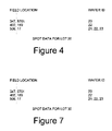
- FIG. 4 is a diagram of a data structure generated by the exemplary process.
- FIG. 5 is a diagram of another data structure generated by the exemplary process.
- FIG. 6 is a diagram of yet another data structure generated by the exemplary process.
- FIG. 7 is a diagram of yet another data structure generated by the exemplary process.
- FIG. 1 shows exemplary manufacturing system 1 , including people, hardware, data, and computer program instructions to carry out certain functions described below.
- Manufacturing system 1 effects step 110 that produces a lot 20 of 18 processed semiconductor wafers, including processed wafers 21 , 22 , and 23 , and sends lot 20 to step 120 .
- Step 120 examines wafers 21 , 22 , and 23 and selectively sends certain wafers to subsequent manufacturing step 130 , and selectively sends other wafers to back to step 110 for rework.
- Rework includes removing a layer of coating, reapplying coating, and reperforming exposure and developing steps.
- FIG. 2 shows an aspect of manufacturing step 120 .
- Wafer 21 includes substrate 2 having an upper surface 4 upon which a pattern is formed in photoresist layer 5 , and a lower surface 6 supported by upper surface 8 of chuck 10 .
- Defect source 12 (in this case, a foreign particulate) is located between lower surface 6 of substrate 2 and upper surface 8 of chuck 10 and creates localized elevation 14 on upper surface 4 of substrate 2 .
- localized elevation 14 results in a hotspot.
- Camera 205 and processor 210 generate focus parameter data related to the topography of upper surface 4 of substrate 2 in order to properly pattern an image in resist layer 5 on surface 4 .
- analyzing the focus parameter data across multiple wafers, and multiple lots provides insight into defect source 12 causing the imaging failure, permitting the original source of the defect to be eliminated.
- analyzing the focus parameter data can differentiate between defect source 12 residing on the chuck 10 or an incoming wafer itself, permitting a proper response to the problem.
- FIG. 3 shows a subflow of processing performed in manufacturing step 120 .
- Camera 205 collects a respective planar image of the upper surface of each wafer of lot 20 . More specifically, the system places a wafer on chuck 10 , collects image data from the wafer while it is on chuck 10 , removes the wafer, and then places the next wafer on the lot on chuck 10 , until the system has collected image data for each wafer of the lot. (step 2 ).
- Processor 210 normalizes the results of step 2 , by partitioning the data into radial bands, and then averaging the data within each band, thereby establishing a height baseline for each band. (step 3 ).
- Processor 210 removes defect data at coordinates associated with defects on a previously processed wafer (step 5 ). Step 5 tends to avoid confusion between a new defect and a previously detected defect.
- Processor 210 determines if a defect exists, according to user settable parameters, including spot size and radial limit, spots outside of the radial limit not being considered defects. (step 10 ).
- step 10 If the result of step 10 is NO, system 1 assigns the lot a value of 0 and sends all wafers of the lot to the next manufacturing step 130 . System 1 then uses chuck 10 to process the next lot, without cleaning chuck 10 . (step 12 ).
- processor 210 determines if a defect is of concern, according to user settable parameters, including spot size and radial limit, defects outside of the radial limit not being considered of concern.
- Another user settable parameter is an allowable percentage of defects on a wafer; a ratio of number of spots/number of fields (step 15 ).
- processor 210 determines if the chuck 10 has a repeating defect, according to user settable chuck limits based on tool type. Chuck limits may include height (based on wavelength), % of defects, and radius. (step 20 ).
- a chuck defect exists when each wafer of the current lot manifests an imaging abnormality at a common X/Y coordinate.
- a repeating chuck defect exists when the chuck has a defect for the current lot and the chuck had a defect for a previous lot, since the last time the chuck was cleaned.
- step 20 If the result of step 20 is NO, system 1 assigns the lot a value of +1 (step 30 ), and control passes to step 50 .
- FIG. 5 shows a wafer defect table generated by the processing of step 50 .
- System 1 updates the chuck defect table.
- a chuck defect exists when each wafer of the lot manifests an imaging problem at a common X/Y coordinate. (Step 55 ).
- FIG. 6 shows a chuck defect table generated by the processing of step 55 .
- manufacturing step 120 receives wafer lot 20 , and generates first image data by placing each wafer of lot 20 on chuck 10 , which is a type of platform, and activating camera 205 to receive light (radiation) from the wafer on chuck 10 .
- step 120 sends some of the wafers back to a previous manufacturing step.
- step 120 receives lot 30 , containing 21 wafers, including wafers 21 , 22 , and 23 returning from rework. Step 120 then generates second image data by placing each wafer of lot 30 chuck 10 , and activating camera 205 .
- Circuitry in processor 210 detects whether abnormal first image data exits at a first common location for each of the last 3 wafers of lot 20 placed on chuck 10 , excluding any abnormal image data at a location for wafers that previously had abnormal image data at the location. More specifically, the circuitry uses the first image data to generate the spot data of FIG. 4 , and then effects step 5 of FIG. 3A .
- Circuitry in processor 210 detects whether abnormal second image data exits at a second common location for each of the last 3 wafers of lot 30 placed on chuck 10 , excluding any abnormal image data at a location for wafers that previously had abnormal image data at the location. More specifically, the circuitry uses the second image data to generate the spot data of FIG. 7 , and effects step 5 of FIG. 3A .
- the spot data of FIGS. 4 and 7 is stored in association with the dates and times the data was generated.
- Processor 210 signals to a human operator that chuck 10 should be cleaned if, for the two subsequent lots 20 and 30 , there is the abnormal condition described in the two previous paragraphs.
- wafer 22 is separated out, because it has a repeating defect at the same location, despite having been processed at step 110 multiple times.
- wafers 21 and 23 are passed to step 130 for subsequent processing.
- circuitry encompasses dedicated hardware, and/or programmable hardware, such as a central processing unit (CPU) or reconfigurable logic array, in combination with programming data, such as sequentially fetched CPU instructions or programming data for a reconfigurable array.
- circuitry encompasses, for example, a general-purpose electronic processor programmed with software, acting to carry out a described function.
- the number of chucks in manufacturing step 120 may be only 1, or may be more than 1.
- the processing described above is applied to a respective chuck receiving a set of wafers belonging to a lot. If step 120 has only 1 chuck, the set of wafers is 100% of the lot, as indicated by the detailed example above. If step 120 has two chucks, the set of wafers may be approximately 50% of the wafers of the lot, etc.
Abstract
Disclosed is a method of operating a manufacturing facility. A processor detects whether abnormal first image data exists at a first common location for each of the last N wafers of the first set of wafers to be placed on a platform, excluding any abnormal image data at a location for wafers that previously had abnormal image data at the location; and detects whether abnormal second image data exists at as second common location for each of the last N wafers of the second set to be placed on the platform, excluding any abnormal image data at a location for wafers that previously had abnormal image data at the location. A decision is made whether to clean the platform depending on results from the processor.
Description
1. Field of the Invention
This invention relates generally to systems and methods of manufacturing and, more particularly, to systems and methods of determining a defect source manifested by localized elevation on the surface topography of a semiconductor substrate.
2. Description of Related Art
As the physical dimensions of semiconductor devices continue to decrease, the topography of the semiconductor substrate upon which the integrated circuit devices are formed becomes an important factor. A semiconductor processing step such as photolithography is used to pattern images in a photoresist on the surface of the substrate. The quality of the images formed on the surface of the substrate by photolithography is related to the topography of the substrate since the topography of the substrate can affect the focus of the photolithographic tool. Localized areas of relatively high elevation can result in defocusing of the patterned images in “hotspots”.
Hotspots are typically caused by a defect source such as foreign particulate matter trapped between the substrate and the photolithography aligner chuck upon which the substrate is placed. The foreign particulate matter causes the substrate to bend or deflect resulting in an elevation of a portion of the surface of the substrate above the foreign material. When the elevation deviation is large enough, the imaging surface will be out of focus relative to surrounding images, and imaging failure occurs typically resulting in a nonfunctioning semiconductor device.
When a hotspot is detected, unnecessary maintenance activity may be performed on the chuck when the defect is actually on the incoming substrates.
To address the problem above, a method comprises receiving a first set of wafers, the first set of wafers being part of a first lot; generating first image data by placing each wafer of the first set on a platform and receiving radiation from the wafer on the platform; receiving a second set of wafers, the second set of wafers being part of a second lot; generating second image data by placing each wafer of the second set on the platform and receiving radiation from the wafer on the platform; detecting whether abnormal first image data exits at a first common location for each of the last N wafers of the first set to be placed on the platform, excluding any abnormal image data at a location for wafers that previously had abnormal image data at the location; detecting whether abnormal second image data exits at a second common location for each of the last N wafers of the second set to be placed on the platform, excluding any abnormal image data at a location for wafers that previously had abnormal image data at the location; and conditionally determining whether to clean the platform, depending on results of the first and second detecting steps.
References are made to the following text taken in connection with the accompanying drawings, in which:
The accompanying drawings which are incorporated in and which constitute a part of this specification, illustrate embodiments of the invention and, together with the description, explain the principles of the invention, and additional advantages thereof. Certain drawings are not necessarily to scale, and certain features may be shown larger than relative actual size to facilitate a more clear description of those features. Throughout the drawings, corresponding elements are labeled with corresponding reference numbers.
Camera 205 and processor 210 generate focus parameter data related to the topography of upper surface 4 of substrate 2 in order to properly pattern an image in resist layer 5 on surface 4.
As described in more detail below, analyzing the focus parameter data across multiple wafers, and multiple lots, provides insight into defect source 12 causing the imaging failure, permitting the original source of the defect to be eliminated. In another embodiment, analyzing the focus parameter data can differentiate between defect source 12 residing on the chuck 10 or an incoming wafer itself, permitting a proper response to the problem.
If the result of step 10 is NO, system 1 assigns the lot a value of 0 and sends all wafers of the lot to the next manufacturing step 130. System 1 then uses chuck 10 to process the next lot, without cleaning chuck 10. (step 12).
If the result of step 10 is YES, processor 210 determines if a defect is of concern, according to user settable parameters, including spot size and radial limit, defects outside of the radial limit not being considered of concern. Another user settable parameter is an allowable percentage of defects on a wafer; a ratio of number of spots/number of fields (step 15).
If the result of step 15 is NO, processor 210 determines if the chuck 10 has a repeating defect, according to user settable chuck limits based on tool type. Chuck limits may include height (based on wavelength), % of defects, and radius. (step 20). A chuck defect exists when each wafer of the current lot manifests an imaging abnormality at a common X/Y coordinate. A repeating chuck defect exists when the chuck has a defect for the current lot and the chuck had a defect for a previous lot, since the last time the chuck was cleaned.
If the result of step 20 is NO, system 1 assigns the lot a value of +1 (step 30), and control passes to step 50.
The data generated by the processing of step 3, shown in FIG. 4 , is an input to the processing of step 50. FIG. 5 shows a wafer defect table generated by the processing of step 50.
The data generated by the processing of step 3, shown in FIG. 4 , is an input to the processing of step 55. FIG. 6 shows a chuck defect table generated by the processing of step 55.
In summary, at a time t1 (FIG. 1 ) manufacturing step 120 receives wafer lot 20, and generates first image data by placing each wafer of lot 20 on chuck 10, which is a type of platform, and activating camera 205 to receive light (radiation) from the wafer on chuck 10.
At a time t2 step 120 sends some of the wafers back to a previous manufacturing step.
At a time t3 step 120 receives lot 30, containing 21 wafers, including wafers 21, 22, and 23 returning from rework. Step 120 then generates second image data by placing each wafer of lot 30 chuck 10, and activating camera 205.
Circuitry in processor 210 detects whether abnormal first image data exits at a first common location for each of the last 3 wafers of lot 20 placed on chuck 10, excluding any abnormal image data at a location for wafers that previously had abnormal image data at the location. More specifically, the circuitry uses the first image data to generate the spot data of FIG. 4 , and then effects step 5 of FIG. 3A .
Circuitry in processor 210 detects whether abnormal second image data exits at a second common location for each of the last 3 wafers of lot 30 placed on chuck 10, excluding any abnormal image data at a location for wafers that previously had abnormal image data at the location. More specifically, the circuitry uses the second image data to generate the spot data of FIG. 7 , and effects step 5 of FIG. 3A .
The spot data of FIGS. 4 and 7 is stored in association with the dates and times the data was generated.
At a time t4, wafer 22 is separated out, because it has a repeating defect at the same location, despite having been processed at step 110 multiple times. On the other hand, at a time t5 wafers 21 and 23 are passed to step 130 for subsequent processing.
In this patent application, the word circuitry encompasses dedicated hardware, and/or programmable hardware, such as a central processing unit (CPU) or reconfigurable logic array, in combination with programming data, such as sequentially fetched CPU instructions or programming data for a reconfigurable array. Thus, circuitry encompasses, for example, a general-purpose electronic processor programmed with software, acting to carry out a described function.
Throughout this patent application, certain processing may be depicted in serial, parallel, or other fashion, for ease of description. Actual hardware and software realizations, however, may be varied depending on desired optimizations apparent to one of ordinary skill in the art. For example, the number of chucks in manufacturing step 120 may be only 1, or may be more than 1. The processing described above is applied to a respective chuck receiving a set of wafers belonging to a lot. If step 120 has only 1 chuck, the set of wafers is 100% of the lot, as indicated by the detailed example above. If step 120 has two chucks, the set of wafers may be approximately 50% of the wafers of the lot, etc.
Additional advantages and modifications will readily occur to those skilled in the art. The invention in its broader aspects is therefore not limited to the specific details, representative apparatus, and illustrative examples shown and described. Accordingly, departures may be made from such details without departing from the spirit or the scope of Applicants' general inventive concept. The invention is defined in the following claims. In general, the words “first,” “second,” etc., employed in the claims do not necessarily denote an order.
Claims (1)
1. A method comprising:
receiving a first set of wafers, the first set of wafers being part of a first lot;
generating first image data by placing each wafer of the first set on a platform and receiving radiation from the wafer on the platform;
receiving a second set of wafers, the second set of wafers being part of a second lot;
generating second image data by placing each wafer of the second set on the platform and receiving radiation from the wafer on the platform;
detecting, using a processor, whether abnormal first image data exists at a first common location for each of the last N wafers of the first set to be placed on the platform, excluding any abnormal image data at a location for wafers that previously had abnormal image data at the location;
detecting, using the processor, whether abnormal second image data exists at a second common location for each of the last N wafers of the second set to be placed on the platform, excluding any abnormal image data at a location for wafers that previously had abnormal image data at the location; and
conditionally determining whether to clean the platform, depending on results of the first and second detecting steps.
Priority Applications (1)
| Application Number | Priority Date | Filing Date | Title |
|---|---|---|---|
| US12/112,027 US7519216B1 (en) | 2008-04-30 | 2008-04-30 | Systems and methods of maintaining equipment for manufacturing semiconductor devices |
Applications Claiming Priority (1)
| Application Number | Priority Date | Filing Date | Title |
|---|---|---|---|
| US12/112,027 US7519216B1 (en) | 2008-04-30 | 2008-04-30 | Systems and methods of maintaining equipment for manufacturing semiconductor devices |
Publications (1)
| Publication Number | Publication Date |
|---|---|
| US7519216B1 true US7519216B1 (en) | 2009-04-14 |
Family
ID=40525185
Family Applications (1)
| Application Number | Title | Priority Date | Filing Date |
|---|---|---|---|
| US12/112,027 Expired - Fee Related US7519216B1 (en) | 2008-04-30 | 2008-04-30 | Systems and methods of maintaining equipment for manufacturing semiconductor devices |
Country Status (1)
| Country | Link |
|---|---|
| US (1) | US7519216B1 (en) |
Cited By (2)
| Publication number | Priority date | Publication date | Assignee | Title |
|---|---|---|---|---|
| US20060258023A1 (en) * | 2005-05-10 | 2006-11-16 | Lsi Logic Corporation | Method and system for improving integrated circuit manufacturing yield |
| US20200051235A1 (en) * | 2018-08-10 | 2020-02-13 | Micron Technology, Inc. | System for predicting properties of structures, imager system, and related methods |
Citations (4)
| Publication number | Priority date | Publication date | Assignee | Title |
|---|---|---|---|---|
| US5673208A (en) | 1996-04-11 | 1997-09-30 | Micron Technology, Inc. | Focus spot detection method and system |
| US6968288B2 (en) | 2003-08-04 | 2005-11-22 | International Business Machines Corporation | Method for detection of photolithographic defocus |
| US7228193B2 (en) | 2005-08-15 | 2007-06-05 | Texas Instruments Incorporated | Methods for detecting structure dependent process defects |
| US20080081385A1 (en) | 2003-07-03 | 2008-04-03 | Marella Paul F | Methods and systems for inspection of wafers and reticles using designer intent data |
-
2008
- 2008-04-30 US US12/112,027 patent/US7519216B1/en not_active Expired - Fee Related
Patent Citations (4)
| Publication number | Priority date | Publication date | Assignee | Title |
|---|---|---|---|---|
| US5673208A (en) | 1996-04-11 | 1997-09-30 | Micron Technology, Inc. | Focus spot detection method and system |
| US20080081385A1 (en) | 2003-07-03 | 2008-04-03 | Marella Paul F | Methods and systems for inspection of wafers and reticles using designer intent data |
| US6968288B2 (en) | 2003-08-04 | 2005-11-22 | International Business Machines Corporation | Method for detection of photolithographic defocus |
| US7228193B2 (en) | 2005-08-15 | 2007-06-05 | Texas Instruments Incorporated | Methods for detecting structure dependent process defects |
Cited By (4)
| Publication number | Priority date | Publication date | Assignee | Title |
|---|---|---|---|---|
| US20060258023A1 (en) * | 2005-05-10 | 2006-11-16 | Lsi Logic Corporation | Method and system for improving integrated circuit manufacturing yield |
| US20200051235A1 (en) * | 2018-08-10 | 2020-02-13 | Micron Technology, Inc. | System for predicting properties of structures, imager system, and related methods |
| US10872403B2 (en) * | 2018-08-10 | 2020-12-22 | Micron Technology, Inc. | System for predicting properties of structures, imager system, and related methods |
| US11869178B2 (en) | 2018-08-10 | 2024-01-09 | Micron Technology, Inc. | System for predicting properties of structures, imager system, and related methods |
Similar Documents
| Publication | Publication Date | Title |
|---|---|---|
| US8617410B2 (en) | Method and system for wafer inspection | |
| US10520450B2 (en) | Substrate inspection method, substrate treatment system, and computer storage medium | |
| US9417191B2 (en) | Using reflected and transmission maps to detect reticle degradation | |
| JP4722038B2 (en) | Single tool defect classification solution | |
| JP5566265B2 (en) | Substrate processing apparatus, program, computer storage medium, and substrate transfer method | |
| US10401305B2 (en) | Time-varying intensity map generation for reticles | |
| KR102631174B1 (en) | Board inspection method, computer storage medium, and board inspection device | |
| EP0898300A2 (en) | Method and apparatus for processing a semiconductor wafer on a robotic track having access to in situ wafer backside particle detection | |
| US9269135B2 (en) | Defect management systems and methods | |
| CN1846170A (en) | Methods and systems for inspection of wafers and reticles using designer intent data | |
| US7469057B2 (en) | System and method for inspecting errors on a wafer | |
| JP2002198289A (en) | Manufacturing method of semiconductor integrated circuit device | |
| De Simone et al. | Exploring the readiness of EUV photo materials for patterning advanced technology nodes | |
| JP5837649B2 (en) | Substrate processing apparatus, abnormality processing unit determination method, program, and computer storage medium | |
| US7519216B1 (en) | Systems and methods of maintaining equipment for manufacturing semiconductor devices | |
| US20070076942A1 (en) | Semiconductor device manufacturing system | |
| TWI434148B (en) | Exposure control system and exposure control method | |
| JP2003243295A (en) | Substrate processing apparatus | |
| JP2011044554A (en) | Exposure control apparatus, and method of manufacturing semiconductor device | |
| JP6423064B2 (en) | Substrate processing system | |
| US8148054B2 (en) | Immersion multiple-exposure method and immersion exposure system for separately performing multiple exposure of micropatterns and non-micropatterns | |
| US7045019B1 (en) | Method for performing site-specific backside particle and contamination removal | |
| JP3523819B2 (en) | Substrate processing equipment | |
| JP2006323030A (en) | Method and device for inspecting photomask, and device and method for manufacturing photomask | |
| JP6047408B2 (en) | Substrate processing apparatus and substrate processing method |
Legal Events
| Date | Code | Title | Description |
|---|---|---|---|
| AS | Assignment |
Owner name: INTERNATIONAL BUSINESS MACHINES CORPORATION, NEW Y Free format text: ASSIGNMENT OF ASSIGNORS INTEREST;ASSIGNORS:POSTIGLIONE, MARC J.;IANNUCCI, JAMES V.;REEL/FRAME:020877/0144 Effective date: 20080429 |
|
| FEPP | Fee payment procedure |
Free format text: PAYOR NUMBER ASSIGNED (ORIGINAL EVENT CODE: ASPN); ENTITY STATUS OF PATENT OWNER: LARGE ENTITY |
|
| REMI | Maintenance fee reminder mailed | ||
| LAPS | Lapse for failure to pay maintenance fees | ||
| STCH | Information on status: patent discontinuation |
Free format text: PATENT EXPIRED DUE TO NONPAYMENT OF MAINTENANCE FEES UNDER 37 CFR 1.362 |
|
| FP | Lapsed due to failure to pay maintenance fee |
Effective date: 20130414 |