US7529336B2 - System and method for laminography inspection - Google Patents
System and method for laminography inspection Download PDFInfo
- Publication number
- US7529336B2 US7529336B2 US11/756,503 US75650307A US7529336B2 US 7529336 B2 US7529336 B2 US 7529336B2 US 75650307 A US75650307 A US 75650307A US 7529336 B2 US7529336 B2 US 7529336B2
- Authority
- US
- United States
- Prior art keywords
- test object
- image
- detectors
- irradiation source
- shift
- Prior art date
- Legal status (The legal status is an assumption and is not a legal conclusion. Google has not performed a legal analysis and makes no representation as to the accuracy of the status listed.)
- Active
Links
Images


Classifications
-
- G—PHYSICS
- G01—MEASURING; TESTING
- G01N—INVESTIGATING OR ANALYSING MATERIALS BY DETERMINING THEIR CHEMICAL OR PHYSICAL PROPERTIES
- G01N23/00—Investigating or analysing materials by the use of wave or particle radiation, e.g. X-rays or neutrons, not covered by groups G01N3/00 – G01N17/00, G01N21/00 or G01N22/00
- G01N23/02—Investigating or analysing materials by the use of wave or particle radiation, e.g. X-rays or neutrons, not covered by groups G01N3/00 – G01N17/00, G01N21/00 or G01N22/00 by transmitting the radiation through the material
- G01N23/04—Investigating or analysing materials by the use of wave or particle radiation, e.g. X-rays or neutrons, not covered by groups G01N3/00 – G01N17/00, G01N21/00 or G01N22/00 by transmitting the radiation through the material and forming images of the material
- G01N23/044—Investigating or analysing materials by the use of wave or particle radiation, e.g. X-rays or neutrons, not covered by groups G01N3/00 – G01N17/00, G01N21/00 or G01N22/00 by transmitting the radiation through the material and forming images of the material using laminography or tomosynthesis
-
- G—PHYSICS
- G01—MEASURING; TESTING
- G01N—INVESTIGATING OR ANALYSING MATERIALS BY DETERMINING THEIR CHEMICAL OR PHYSICAL PROPERTIES
- G01N23/00—Investigating or analysing materials by the use of wave or particle radiation, e.g. X-rays or neutrons, not covered by groups G01N3/00 – G01N17/00, G01N21/00 or G01N22/00
- G01N23/02—Investigating or analysing materials by the use of wave or particle radiation, e.g. X-rays or neutrons, not covered by groups G01N3/00 – G01N17/00, G01N21/00 or G01N22/00 by transmitting the radiation through the material
- G01N23/04—Investigating or analysing materials by the use of wave or particle radiation, e.g. X-rays or neutrons, not covered by groups G01N3/00 – G01N17/00, G01N21/00 or G01N22/00 by transmitting the radiation through the material and forming images of the material
- G01N23/046—Investigating or analysing materials by the use of wave or particle radiation, e.g. X-rays or neutrons, not covered by groups G01N3/00 – G01N17/00, G01N21/00 or G01N22/00 by transmitting the radiation through the material and forming images of the material using tomography, e.g. computed tomography [CT]
-
- G—PHYSICS
- G01—MEASURING; TESTING
- G01N—INVESTIGATING OR ANALYSING MATERIALS BY DETERMINING THEIR CHEMICAL OR PHYSICAL PROPERTIES
- G01N2223/00—Investigating materials by wave or particle radiation
- G01N2223/40—Imaging
- G01N2223/419—Imaging computed tomograph
Definitions
- the present invention generally relates to imaging techniques for industrial inspection, and more specifically to systems and methods for laminography inspection.
- X-ray laminography is a well-known imaging technique that generates cross-sectional images of selected planes within a test object for inspection.
- the X-ray laminography system includes an X-ray source, X-ray detectors defining an image plane, and a fixture base for placement of the test object to be scanned between the X-ray source and the detectors.
- the test object is usually scanned through a cycle of coordinated motion of either the X-ray source along with the detectors or the fixture base alone.
- the configuration of the X-ray source, test object, and detectors is such that any point in a specific plane of the test object, also called “focal plane”, is always projected to the same point in the image plane, while any point outside the focal plane is projected to a plurality of points in the image plane.
- the image of the focal plane will appear sharp while the images of other planes within the test object will experience movement with respect to the detectors, creating a blurred background upon which is superimposed the sharp image of the focal plane.
- a cross-sectional image of a selected section within the test object is reconstructed by a combination of the acquired images.
- One known approach implements a laminography system in which the X-ray source and detectors scan the fixed test object along a circular path to acquire images of the test object.
- a “stop-and-go” motion is performed to acquire images under different viewing angles at discrete points on the circular path.
- the scanning speed is relatively slow and the number of acquired images is limited.
- the driving mechanism for a rotational scanning cycle is bulky and expensive and requires a complex manufacturing process.
- Another known approach uses a single translational scan for acquiring images of the test object under different viewing angles.
- the X-ray source has to be collimated to irradiate beam fans of X-rays that cover the entire width of the test object.
- an increased number of X-ray detectors is required so that the image data acquired with a single linear scanning pass are from a sufficient number of viewing angles.
- this laminography system performs a simple and fast scanning cycle, the greater amount of requisite detectors still contributes to an increase in the equipment cost.
- the required collimation of the X-ray source adds complexity to the laminography system.
- a warp in the test object may result in a position of the section of interest that is actually biased relative to its assumed position.
- the laminographic cross-sectional image actually reconstructed may not represent the selected section plane, but another one offset from the desired section plane.
- U.S. Pat. No. 5,678,209 describes a warp compensation mode of operation, the disclosure of which is incorporated herein by reference.
- This known warp compensation technique requires the use of predetermined computer-assisted design (CAD) data of the test object that are to be compared against captured image data of the test object to determine the warp of the test object.
- CAD computer-assisted design
- the image shifts to be applied to reconstruct a cross-section image of the selected section then are determined. Practically, the application of this technique is inaccurate as the selected features often are not placed at the exact CAD position or the CAD data of the test objects are not available at all.
- the present application describes a system and method for laminography inspection that can effectively generate a cross-sectional image of a selected section plane within a test object using a convenient warp compensation mode of computation.
- the laminography inspection system comprises an irradiation source, a plurality of linear image detectors defining an image plane, a fixed table for placement of a test object in a stationary position between the irradiation source and the image detectors, and a computing device for processing a plurality of images of the test object acquired from the image detectors.
- the irradiation source and the image detectors perform a scanning cycle comprised of parallel linear scanning passes spanning across the area of the test object. Images of the test object are thereby acquired under different viewing angles for processing by the computing device.
- the computing device combines the acquired images being adequately shifted and scaled to generate a cross-sectional image of a selected section within the test object.
- the computing device may be configured to determine a warp compensation that is applied to the computation of the shift and scale factors for combining the acquired images of the test object.
- the warp compensation may be computed with a stereo imaging method.
- One advantage of the system and method according to the present invention is that it is cost efficient, and allows for a convenient warp compensation mode of computation that does not require CAD data of the test object.
- FIG. 1A is a schematic perspective view of a laminography inspection system according to one embodiment of the invention.
- FIG. 1B is a schematic side view of a laminography inspection system according to one embodiment of the invention.
- FIG. 1C is a schematic diagram illustrating a scanning operation performed within a laminography inspection system according to one embodiment of the invention
- FIGS. 2A through 2D are schematic views showing the principles for reconstructing an X-ray image of a section within a test object according to the present invention
- FIG. 2E illustrate the determination of a warp compensation according to the present invention
- FIG. 3 is a flowchart of method steps performed within a laminography inspection system according to one embodiment of the invention.
- FIGS. 4A through 4E show exemplary samples of X-ray images which may be obtained with a laminography inspection method according to the present invention.
- the present application describes a system and method for laminography inspection that is cost efficient, and can effectively generate a cross-sectional image of a selected section plane within a test object using a convenient warp compensation mode of computation.
- irradiation source means an energetic source configured to emit electromagnetic radiations used for radiography, including, but not limited to, X-ray sources, gamma sources, or the like.
- image detector means a device configured to produce image signals of a test object as it receives radiations traveling from the irradiation source through the test object, including, but not limited to, X-ray detectors, gamma detectors, or the like.
- FIGS. 1A and 1B are schematic views illustrating a laminography inspection system according to one embodiment of the present invention.
- Inspection system 100 includes an X-ray source 102 , a fixed table 104 for placement of an object 106 under examination, linear X-ray detectors 108 , and a computing device 110 .
- the X-ray source 102 is positioned above the fixed table 104 and may irradiate a conical beam of X-rays that travels through the object 106 and impinges on the detectors 108 lying underneath the object 106 opposite to the X-ray source 102 .
- Each of the linear detectors 108 converts a pattern of X-rays that passed through the object 106 into image signals that are transmitted to the computing device 110 for analysis.
- the fixed table 104 is stationary in a horizontal plane parallel to the axes X and Y.
- the X-ray source 102 is mounted on a vertical axle parallel to axis Z and perpendicular to the plane of the fixed table 104 .
- the X-ray source 102 is independently driven along the axes X, Y and Z by a motor drive mechanism (not shown).
- the X-ray source 102 may include, but is not limited to, any standard industrial X-ray tubes.
- the linear X-ray detectors 108 are placed coplanar on a support frame 112 at fixed spaced intervals along the axis X, and lie parallel to the axis Y.
- a number of 3 linear detectors 108 may be provided, each of which is formed from linear or one-dimensional arrays of discrete X-ray sensitive elements similar to charge coupled devices.
- the support frame 112 can be independently driven along the axes X, Y and Z so as to desirably set the position of the detectors 108 relative to the test object 106 and X-ray source 102 .
- the relative positions of the X-ray source 102 and the linear detectors 108 may be adjusted in order to set a desired focal plane and optimal resolution for the acquisition of X-ray images.
- FIG. 1C describes a preferred scanning cycle performed by the inspection system 100 according to one embodiment.
- the test object 106 is stationary while the X-ray source 102 synchronously moves with the detectors 106 to scan the test object 106 .
- the scanning cycle includes linear scanning passes 114 that are parallel to the axis X and sequentially increment with respect to the axis Y to span across the area of the test object 106 .
- X-ray image data of a scanned portion of the test object 106 are respectively obtained from the 3 linear detectors 108 under 3 different viewing angles corresponding to the X-ray source 102 .
- the Y-increment between successive passes may be set so that the adjacent scanning passes will overlap.
- the number of viewing angles can be increased by the number of scanning passes covering the scanned portion.
- more X-ray image data of different viewing angles may be acquired for analysis by the computing device 110 without adding any image detectors or costly scanning motions.
- increment between two successive passes may also be set differently, and the overlap described above is not mandatory.
- a different embodiment may use one single detector to perform 3 linear scanning passes under different viewing angles relative to the X-ray source 102 to acquire the same images under 3 viewing angles. Based on the acquired images, the computing device 110 is configured to generate laminographic images for inspection of the test object 106 .
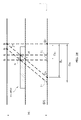
- FIGS. 2A through 2D are schematic diagrams illustrating the geometric principles for reconstructing an X-ray image of a section P within the test object based on a combination of X-ray image data acquired under different viewing angles.
- Distance H 1 separates the X-ray source S from the image plane D where are positioned the detectors D 1 , D 2 and D 3 .
- Detector D 1 is arranged at a left angled position relative to source S
- detector D 2 is arranged at a vertical position opposite to the source S
- detector D 3 is arranged at a right angled position relative to source S.
- Distance H 0 denotes the distance between the focal plane F and the X-ray source S.
- Distance h denotes the distance between an object section of interest P and the focal plane F.
- Distance R x separates two adjacent detectors, while length R y corresponds to a Y-increment between two successive scanning passes.
- a section within the test object 106 that is outside the focal plane F will form different images that are distorted and shifted from one another in the image plane D.
- the image plane D only images of points in the focal plane F will appear sharp while points outside the focal plane F will appear blurred.
- the X-ray image data acquired under different viewing angles are combined with adequate shift and scale factors so that they properly overlap to generate a suitable image of the section of interest P. These shift and scale factors may be determined relative to the axes X and Y as detailed below.
- FIG. 2B illustrates the determination of the scale and shift factors in the direction X based on a projection plane parallel to the axes X and Z. From a viewpoint in this projection plane, one point O in the focal plane F will correspond to an image point O i in the image plane D, and a point O h in the section of interest P vertically above point O will correspond to the image point O hi in the image plane D.
- a segment O h M in the direction X within a section plane P of the test object 106 will project into the image plane D without distortion.
- the scale factor in the direction X thus is equal to 1.
- FIG. 2C illustrates the determination of a shift factor L sy in the direction Y based on a projection plane parallel to the axes Y and Z. From a viewpoint in this projection plane, point O in the focal plane F will form an image point O i ′ in the image plane D, and point O h ′ in the object section of interest P vertically above point O will form the image point O hi ′ in the image plane D.
- FIG. 2D illustrates the determination of a scale factor f in the direction Y made in a projected plane parallel to the axes Y and Z.
- Table 1 describes the different shift and scale factors in the direction X and Y computed for reconstructing an X-ray image of a desired section within the test object defined by its height h relative to the focal plane.
- the combined X-ray images of the test object adequately overlap to form a reconstructed image of a desired section at a coordinate Z in the test object.
- the illustrated technique for Z-axis warp compensation uses a stereo imaging method to construct a Z-map that characterizes a warp in the test object.
- two images I 2 and I 1 will be respectively acquired by detectors D 2 and D 1 for a feature W of the test object at a height H relative to a surface reference.
- D n and D h represent the respective positions of the images I 2 and I 1 and r(0) is the image resolution
- the actual height H of the feature W can be derived from the following formulae:
- a Z-map can be constructed based on the images acquired during the scanning cycle.
- the computing device can apply a warp compensation in the computed shift and scale factors so that a reconstructed laminographic image correctly reflects a selected section P of the test object, even if it is actually located at a biased position due to the occurrence of a warp in the test object. Effective warp compensation thus can be computed without the need of CAD data of the test object.
- step 302 the test object 106 is placed in the inspection system 100 .
- initial settings are made in step 304 to define the focal plane and an adequate image resolution by adjusting the relative positions between the X-ray source 102 , the object 106 and the detectors 108 .
- step 306 a scanning operation then is performed, by which the X-ray source 102 irradiating a conical beam of X-rays synchronously moves with the detectors 106 along parallel linear scanning passes across the area of the fixed object 106 .
- Multiple X-ray images of the test object 106 under different viewing angles are thereby acquired to reconstruct a cross-sectional image of a section of interest P within the test object 106 .
- the inspection system 100 requests the operator to input the height h of the desired section P relative to the focal plane F.
- the computing device 110 may compute an object warp compensation to be applied in the reconstruction of the cross-sectional image of the selected section P.
- the computation of the warp compensation may be achieved by constructing a Z-map characteristic of a warp of the test object based on the acquired X-ray images, as described above in conjunction with FIG. 2E .
- step 312 based on the inputted height h and the computed warp compensation, the computing device 110 calculates the proper shift and scale factors and applies these factors to combine the acquired X-ray images in order to generate a cross-sectional image of the selected section P.
- FIGS. 4A through 4E show exemplary samples of images which may be obtained through a laminography inspection method according to the present invention.
- FIG. 4A schematically shows the configuration of the test object, which includes two layers 410 and 420 of solders respectively arranged in two parallel planes lying over each other. Each of the layers 410 and 420 includes a 3 ⁇ 3 array of solders.
- the illustrated gap “g” between the two layers 410 and 420 and inter-solder pitch “p” are expressed with arbitrary units.
- the test object includes a number of defects 412 , 418 , 424 , 428 and 429 that will be apparent from the reconstructed X-ray images discussed below with reference to FIGS. 4B through 4E .
- the reconstructed X-ray images 402 and 404 correctly show the presence of a solder bridge defect 418 connecting between solders 412 and 414 and void defect 416 within the solder 412 .
- the reconstructed X-ray images 406 and 408 correctly show the presences of a solder bridge defect 428 connecting with solder 426 and void defect 424 within the solder 422 .
- the method and system according to the principles of the present invention can effectively reconstruct a cross-sectional image of a section of interest within the test object based on images acquired by the image detectors.
- the image acquisition is achieved through a cycle of parallel linear scanning passes that efficiently increases the number of viewing angles without adding image detectors.
Abstract
Description
L sx =h×tan θ=h R x /H 1
L sy =h′×tan θ′
L sy =h×R y/(H 0 −h)
f=(H 1 −h′)/H 1=1−h/H 0
| TABLE 1 | |||
| X | Y | ||
| shift factor |
|
|
| scale factor | 1 |
|
Claims (14)
Priority Applications (5)
| Application Number | Priority Date | Filing Date | Title |
|---|---|---|---|
| US11/756,503 US7529336B2 (en) | 2007-05-31 | 2007-05-31 | System and method for laminography inspection |
| TW096127817A TWI349774B (en) | 2007-05-31 | 2007-07-30 | System and method for laminography inspection |
| JP2007205520A JP4551919B2 (en) | 2007-05-31 | 2007-08-07 | Tomographic inspection system and method |
| CNU2007201571922U CN201199234Y (en) | 2007-05-31 | 2007-08-14 | Layered photodetection system |
| CN200710140075XA CN101315341B (en) | 2007-05-31 | 2007-08-14 | System and method for laminography inspection |
Applications Claiming Priority (1)
| Application Number | Priority Date | Filing Date | Title |
|---|---|---|---|
| US11/756,503 US7529336B2 (en) | 2007-05-31 | 2007-05-31 | System and method for laminography inspection |
Publications (2)
| Publication Number | Publication Date |
|---|---|
| US20080298538A1 US20080298538A1 (en) | 2008-12-04 |
| US7529336B2 true US7529336B2 (en) | 2009-05-05 |
Family
ID=40088189
Family Applications (1)
| Application Number | Title | Priority Date | Filing Date |
|---|---|---|---|
| US11/756,503 Active US7529336B2 (en) | 2007-05-31 | 2007-05-31 | System and method for laminography inspection |
Country Status (4)
| Country | Link |
|---|---|
| US (1) | US7529336B2 (en) |
| JP (1) | JP4551919B2 (en) |
| CN (2) | CN201199234Y (en) |
| TW (1) | TWI349774B (en) |
Cited By (7)
| Publication number | Priority date | Publication date | Assignee | Title |
|---|---|---|---|---|
| US20080089567A1 (en) * | 2006-10-11 | 2008-04-17 | Eliasson Tracy K | Artifact reduction in an x-ray imaging system |
| US20090232277A1 (en) * | 2008-03-14 | 2009-09-17 | General Electric Company | System and method for inspection of items of interest in objects |
| DE102009051045A1 (en) * | 2009-10-26 | 2011-04-28 | Göpel electronic GmbH | Method and device for 3-dimensional testing by means of X-radiation |
| US20110255660A1 (en) * | 2008-12-22 | 2011-10-20 | Omron Corporation | X-ray inspection method and x-ray inspection apparatus |
| US20170184514A1 (en) * | 2008-11-11 | 2017-06-29 | Hamamatsu Photonics K.K. | Radiation detection device, radiation image acquiring system, radiation inspection system, and radiation detection method |
| US9791387B2 (en) | 2014-09-26 | 2017-10-17 | Test Research, Inc. | Inspection system and method for controlling the same |
| US11022570B2 (en) * | 2018-08-03 | 2021-06-01 | Hitachi High-Tech Science Corporation | X-ray transmission inspection apparatus and X-ray transmission inspection method |
Families Citing this family (17)
| Publication number | Priority date | Publication date | Assignee | Title |
|---|---|---|---|---|
| US7529336B2 (en) * | 2007-05-31 | 2009-05-05 | Test Research, Inc. | System and method for laminography inspection |
| US20110249795A1 (en) * | 2008-12-22 | 2011-10-13 | Omron Corporation | X-ray inspection method and x-ray inspection apparatus |
| GB0902138D0 (en) * | 2009-02-10 | 2009-03-25 | Durham Scient Crystals Ltd | Apparatus and method for viewing an object |
| JP5544636B2 (en) * | 2009-10-20 | 2014-07-09 | 東芝Itコントロールシステム株式会社 | Tomography equipment |
| CN101839871B (en) * | 2010-05-18 | 2011-12-28 | 华南理工大学 | X-ray layered photography detection method and system |
| CN103278515A (en) * | 2013-05-16 | 2013-09-04 | 华南理工大学 | Rotary X-ray layered photographic detection system and method |
| CN103558862B (en) * | 2013-10-21 | 2017-04-05 | 华南理工大学 | A kind of autonomous precision Tracing Control system and method for X-ray image point |
| EP3040713B2 (en) * | 2014-12-30 | 2021-08-04 | VisiConsult X-ray Systems & Solutions GmbH | Device for automatically recognising errors on workpieces |
| US9841387B2 (en) * | 2015-07-22 | 2017-12-12 | Test Research, Inc. | Inspection method and device |
| CN107202808A (en) * | 2017-06-14 | 2017-09-26 | 上海英曼尼安全装备有限公司 | A kind of double source double-visual angle safety inspection method and its system |
| CN107436308B (en) * | 2017-09-15 | 2024-02-09 | 中国特种设备检测研究院 | CT (computed tomography) chromatographic scanning device for plate-shaped workpiece |
| CN110596162B (en) * | 2019-09-19 | 2021-02-26 | 西安交通大学 | Calibration device based on monochromatic X-ray diffraction |
| TWI724696B (en) | 2019-12-18 | 2021-04-11 | 財團法人工業技術研究院 | Workpiece hole measurement method |
| JP6973536B2 (en) * | 2020-03-11 | 2021-12-01 | オムロン株式会社 | X-ray inspection equipment and X-ray inspection method |
| CN115598152A (en) * | 2021-07-07 | 2023-01-13 | 同方威视技术股份有限公司(Cn) | Radiation imaging system and radiation imaging method |
| CN115963124B (en) * | 2021-10-08 | 2024-01-26 | 同方威视技术股份有限公司 | CT imaging system |
| WO2023177981A1 (en) * | 2022-03-15 | 2023-09-21 | Sigray, Inc. | System and method for compact laminography utilizing microfocus transmission x-ray source and variable magnification x-ray detector |
Citations (89)
| Publication number | Priority date | Publication date | Assignee | Title |
|---|---|---|---|---|
| US4926452A (en) | 1987-10-30 | 1990-05-15 | Four Pi Systems Corporation | Automated laminography system for inspection of electronics |
| US5027418A (en) | 1989-02-13 | 1991-06-25 | Matsushita Electric Industrial Co., Ltd. | Electro-optical inspection apparatus for printed-circuit boards with components mounted thereon |
| US5060246A (en) | 1988-10-18 | 1991-10-22 | U.S. Philips Corporation | Computer tomography system with a scanogram |
| US5081656A (en) | 1987-10-30 | 1992-01-14 | Four Pi Systems Corporation | Automated laminography system for inspection of electronics |
| US5097492A (en) | 1987-10-30 | 1992-03-17 | Four Pi Systems Corporation | Automated laminography system for inspection of electronics |
| US5113425A (en) | 1989-06-02 | 1992-05-12 | Glenbrook Technologies, Inc. | X-ray inspection system for electronic components |
| US5164994A (en) | 1989-12-21 | 1992-11-17 | Hughes Aircraft Company | Solder joint locator |
| US5182775A (en) | 1990-01-12 | 1993-01-26 | Kawasaki Jukogyo Kabushiki Kaisha | Method of processing radiographic image data for detecting a welding defect |
| US5199054A (en) | 1990-08-30 | 1993-03-30 | Four Pi Systems Corporation | Method and apparatus for high resolution inspection of electronic items |
| US5259012A (en) | 1990-08-30 | 1993-11-02 | Four Pi Systems Corporation | Laminography system and method with electromagnetically directed multipath radiation source |
| US5289520A (en) | 1991-11-27 | 1994-02-22 | Lorad Corporation | Stereotactic mammography imaging system with prone position examination table and CCD camera |
| US5351278A (en) | 1992-03-09 | 1994-09-27 | Hitachi, Ltd. | X-ray tomography method and apparatus thereof |
| US5388136A (en) | 1992-07-03 | 1995-02-07 | International Business Machines Corporation | X-ray inspection apparatus for electronic circuits |
| US5455870A (en) | 1991-07-10 | 1995-10-03 | Raytheon Company | Apparatus and method for inspection of high component density printed circuit board |
| US5500886A (en) | 1994-04-06 | 1996-03-19 | Thermospectra | X-ray position measuring and calibration device |
| US5524132A (en) | 1995-05-12 | 1996-06-04 | International Business Machines Corporation | Process for revealing defects in testpieces using attenuated high-energy x-rays to form images in reusable photographs |
| US5541856A (en) | 1993-11-08 | 1996-07-30 | Imaging Systems International | X-ray inspection system |
| US5561696A (en) | 1987-10-30 | 1996-10-01 | Hewlett-Packard Company | Method and apparatus for inspecting electrical connections |
| US5583904A (en) | 1995-04-11 | 1996-12-10 | Hewlett-Packard Co. | Continuous linear scan laminography system and method |
| US5592562A (en) | 1994-01-19 | 1997-01-07 | International Business Machines Corporation | Inspection system for cross-sectional imaging |
| US5594770A (en) | 1994-11-18 | 1997-01-14 | Thermospectra Corporation | Method and apparatus for imaging obscured areas of a test object |
| US5594768A (en) | 1994-05-12 | 1997-01-14 | Kabushiki Kaisha Toshiba | Laminograph and inspection and repair device using the same |
| US5621811A (en) | 1987-10-30 | 1997-04-15 | Hewlett-Packard Co. | Learning method and apparatus for detecting and controlling solder defects |
| US5631738A (en) | 1995-08-30 | 1997-05-20 | Hewlett-Packard Co. | Laser ranging system having reduced sensitivity to surface defects |
| US5659483A (en) | 1996-07-12 | 1997-08-19 | National Center For Manufacturing Sciences | System and method for analyzing conductor formation processes |
| US5687209A (en) | 1995-04-11 | 1997-11-11 | Hewlett-Packard Co. | Automatic warp compensation for laminographic circuit board inspection |
| US5751784A (en) | 1996-09-27 | 1998-05-12 | Kevex X-Ray | X-ray tube |
| US5761337A (en) | 1993-05-13 | 1998-06-02 | Sharp Kabushiki Kaisha | Method and apparatus for inspection of the appearance of bumps |
| US6002790A (en) | 1996-12-09 | 1999-12-14 | Advent Engineering Services, Inc. | Method for detecting and measuring voids in conductor insulation systems |
| US6002739A (en) | 1998-04-28 | 1999-12-14 | Hewlett Packard Company | Computed tomography with iterative reconstruction of thin cross-sectional planes |
| US6076411A (en) | 1996-12-09 | 2000-06-20 | Advent Engineering Services, Inc. | Method and apparatus for determining remaining life of conductor insulation systems through void size and density correlation |
| US6084663A (en) | 1997-04-07 | 2000-07-04 | Hewlett-Packard Company | Method and an apparatus for inspection of a printed circuit board assembly |
| US6201850B1 (en) | 1999-01-26 | 2001-03-13 | Agilent Technologies, Inc. | Enhanced thickness calibration and shading correction for automatic X-ray inspection |
| US6222903B1 (en) | 1998-09-30 | 2001-04-24 | Samsung Electronics Co., Ltd. | Laminography system having a view selector with prism |
| US6236709B1 (en) | 1998-05-04 | 2001-05-22 | Ensco, Inc. | Continuous high speed tomographic imaging system and method |
| US6269326B1 (en) | 1996-05-29 | 2001-07-31 | Softlink | Method for testing electronic components |
| US6314201B1 (en) | 1998-10-16 | 2001-11-06 | Agilent Technologies, Inc. | Automatic X-ray determination of solder joint and view delta Z values from a laser mapped reference surface for circuit board inspection using X-ray laminography |
| US6324249B1 (en) | 2001-03-21 | 2001-11-27 | Agilent Technologies, Inc. | Electronic planar laminography system and method |
| US6327333B1 (en) | 1999-03-03 | 2001-12-04 | Bridgestone Corporation | Tire interior inspecting method and tire interior inspecting system for carrying out the same |
| US6373917B1 (en) | 2000-08-30 | 2002-04-16 | Agilent Technologies, Inc. | Z-axis elimination in an X-ray laminography system using image magnification for Z plane adjustment |
| US6445767B1 (en) | 1989-12-05 | 2002-09-03 | University Of Massachussetts Medical Center | System for quantitative radiographic imaging |
| US6463121B1 (en) | 1999-10-13 | 2002-10-08 | General Electric Company | Interactive x-ray position and exposure control using image data as reference information |
| US6480564B1 (en) | 1999-02-02 | 2002-11-12 | Samsung Electronics Co., Ltd. | Sectional image photography system and method thereof |
| US6483890B1 (en) | 2000-12-01 | 2002-11-19 | Koninklijke Philips Electronics, N.V. | Digital x-ray imaging apparatus with a multiple position irradiation source and improved spatial resolution |
| US6485176B1 (en) | 2000-10-12 | 2002-11-26 | Photon Dynamics, Inc. | Inspection system with rho-theta x-ray source transport system |
| US6563905B1 (en) | 2001-10-30 | 2003-05-13 | Qualcomm, Incorporated | Ball grid array X-ray orientation mark |
| US6570954B2 (en) | 2001-01-19 | 2003-05-27 | Koninklijke Philips Electronics N.V. | X-ray device for tomosynthesis |
| US6570957B2 (en) | 1999-09-29 | 2003-05-27 | Siemens Aktiengesellschaft | X-ray diagnostic apparatus having a storage luminescent screen |
| US6618465B2 (en) | 2001-11-12 | 2003-09-09 | General Electric Company | X-ray shielding system and shielded digital radiographic inspection system and method |
| US6628745B1 (en) | 2000-07-01 | 2003-09-30 | Martin Annis | Imaging with digital tomography and a rapidly moving x-ray source |
| US6628746B2 (en) | 2001-10-30 | 2003-09-30 | Agilent Technologies, Inc. | Image-based inspection system including positioning compensation for non-planar targets |
| US6630675B2 (en) | 2000-07-26 | 2003-10-07 | Siemens Medical Solutions Usa, Inc. | X-ray scintillator compositions for X-ray imaging applications |
| US6665433B2 (en) | 2001-07-31 | 2003-12-16 | Agilent Technologies, Inc. | Automatic X-ray determination of solder joint and view Delta Z values from a laser mapped reference surface for circuit board inspection using X-ray laminography |
| US6671349B1 (en) | 2000-11-13 | 2003-12-30 | Olganix Corporation | Tomosynthesis system and registration method |
| US6707877B2 (en) | 2001-09-27 | 2004-03-16 | Agilent Technologies, Inc. | Positioning mechanism providing precision 2-axis rotation, 1-axis translation adjustment |
| US6717415B2 (en) | 2002-02-05 | 2004-04-06 | Logicvision, Inc. | Circuit and method for determining the location of defect in a circuit |
| US6738450B1 (en) | 2002-12-10 | 2004-05-18 | Agilent Technologies, Inc. | System and method for cost-effective classification of an object under inspection |
| US6748046B2 (en) | 2000-12-06 | 2004-06-08 | Teradyne, Inc. | Off-center tomosynthesis |
| US6765981B2 (en) | 2002-07-31 | 2004-07-20 | Agilent Technologies, Inc. | Computed tomography |
| US6819739B2 (en) | 2002-11-27 | 2004-11-16 | Agilent Technologies, Inc. | Method and apparatus for calibrating an x-ray laminography imaging system |
| US6819805B2 (en) | 2001-05-02 | 2004-11-16 | Agilent Technologies, Inc. | Method and apparatus for brightness equalization of images taken with point source illumination |
| US6826255B2 (en) | 2003-03-26 | 2004-11-30 | General Electric Company | X-ray inspection system and method of operating |
| US6825856B1 (en) | 2000-07-26 | 2004-11-30 | Agilent Technologies, Inc. | Method and apparatus for extracting measurement information and setting specifications using three dimensional visualization |
| US6847900B2 (en) | 2001-12-17 | 2005-01-25 | Agilent Technologies, Inc. | System and method for identifying solder joint defects |
| US6850589B2 (en) | 2002-03-27 | 2005-02-01 | Agilent Technologies, Inc. | Tomography of curved surfaces |
| US6853744B2 (en) | 2001-12-14 | 2005-02-08 | Agilent Technologies, Inc. | System and method for confirming electrical connection defects |
| US6872949B2 (en) | 2000-03-28 | 2005-03-29 | Matsushita Electric Industrial Co., Ltd. | Connection inspecting apparatus, connection inspecting method, and recording medium for recording programs executing the method |
| US6885724B2 (en) | 2003-08-22 | 2005-04-26 | Ge Medical Systems Global Technology Company, Llc | Radiographic tomosynthesis image acquisition utilizing asymmetric geometry |
| US6890098B2 (en) | 2002-11-22 | 2005-05-10 | Agilent Technologies, Inc. | Method for calibrating the intensity profile for a movable x-ray source |
| US6895073B2 (en) | 2002-11-22 | 2005-05-17 | Agilent Technologies, Inc. | High-speed x-ray inspection apparatus and method |
| US6895072B2 (en) | 2003-03-26 | 2005-05-17 | Heimann Systems Corp. | Apparatus and method for non-destructive inspection of material in containers |
| US6907103B2 (en) | 2002-06-19 | 2005-06-14 | Agilent Technologies, Inc. | Capturing images of moving objects with a moving illumination point source |
| US6907110B2 (en) | 2002-09-03 | 2005-06-14 | Siemens Aktiengesellschaft | X-ray tube with ring anode, and system employing same |
| US6928185B2 (en) | 2000-06-30 | 2005-08-09 | Nidek Co., Ltd. | Defect inspection method and defect inspection apparatus |
| US6965662B2 (en) | 2002-12-17 | 2005-11-15 | Agilent Technologies, Inc. | Nonplanar x-ray target anode for use in a laminography imaging system |
| US6970531B2 (en) | 2002-10-07 | 2005-11-29 | General Electric Company | Continuous scan RAD tomosynthesis system and method |
| US6977985B2 (en) | 2002-12-17 | 2005-12-20 | Agilent Technologies, Inc. | X-ray laminography system having a pitch, roll and Z-motion positioning system |
| US6980627B2 (en) | 2000-10-06 | 2005-12-27 | Xintek, Inc. | Devices and methods for producing multiple x-ray beams from multiple locations |
| US6993193B2 (en) | 2002-03-26 | 2006-01-31 | Agilent Technologies, Inc. | Method and system of object classification employing dimension reduction |
| US7010086B2 (en) | 2004-01-15 | 2006-03-07 | Agilent Technologies, Inc. | Three-dimensional x-ray imaging system |
| US7099435B2 (en) | 2003-11-15 | 2006-08-29 | Agilent Technologies, Inc | Highly constrained tomography for automated inspection of area arrays |
| US7099432B2 (en) | 2003-08-27 | 2006-08-29 | Matsushita Electric Industrial Co., Ltd. | X-ray inspection apparatus and X-ray inspection method |
| US7108424B2 (en) | 2004-03-11 | 2006-09-19 | Agilent Technologies, Inc. | Method and apparatus for calibration of indirect measurement systems |
| US7110490B2 (en) | 2002-12-10 | 2006-09-19 | General Electric Company | Full field digital tomosynthesis method and apparatus |
| US7123688B2 (en) | 2002-05-31 | 2006-10-17 | Koninklijke Philips Electronics, N.V. | X-ray tube |
| US7171897B2 (en) | 2003-06-05 | 2007-02-06 | Georgia Tech Research Corporation | System and methods for data-driven control of manufacturing processes |
| US7177391B2 (en) | 2005-03-29 | 2007-02-13 | Surescan Corporation | Imaging inspection apparatus |
| US7177389B2 (en) | 2004-01-09 | 2007-02-13 | Adelphi Technology | X-ray tomography and laminography |
| US7231013B2 (en) * | 2003-03-21 | 2007-06-12 | Agilent Technologies, Inc. | Precise x-ray inspection system utilizing multiple linear sensors |
Family Cites Families (4)
| Publication number | Priority date | Publication date | Assignee | Title |
|---|---|---|---|---|
| JPS61155845A (en) * | 1984-12-28 | 1986-07-15 | Toshiba Corp | Tomographic image pickup device |
| JPH0688790A (en) * | 1992-09-07 | 1994-03-29 | Toshiba Corp | Laminography apparatus |
| KR20000007400A (en) * | 1998-07-03 | 2000-02-07 | 윤종용 | Image obtaining method of computer tomography system |
| US7529336B2 (en) * | 2007-05-31 | 2009-05-05 | Test Research, Inc. | System and method for laminography inspection |
-
2007
- 2007-05-31 US US11/756,503 patent/US7529336B2/en active Active
- 2007-07-30 TW TW096127817A patent/TWI349774B/en active
- 2007-08-07 JP JP2007205520A patent/JP4551919B2/en active Active
- 2007-08-14 CN CNU2007201571922U patent/CN201199234Y/en not_active Expired - Lifetime
- 2007-08-14 CN CN200710140075XA patent/CN101315341B/en active Active
Patent Citations (95)
| Publication number | Priority date | Publication date | Assignee | Title |
|---|---|---|---|---|
| US5621811A (en) | 1987-10-30 | 1997-04-15 | Hewlett-Packard Co. | Learning method and apparatus for detecting and controlling solder defects |
| US4926452A (en) | 1987-10-30 | 1990-05-15 | Four Pi Systems Corporation | Automated laminography system for inspection of electronics |
| US5561696A (en) | 1987-10-30 | 1996-10-01 | Hewlett-Packard Company | Method and apparatus for inspecting electrical connections |
| US5291535A (en) | 1987-10-30 | 1994-03-01 | Four Pi Systems Corporation | Method and apparatus for detecting excess/insufficient solder defects |
| US5097492A (en) | 1987-10-30 | 1992-03-17 | Four Pi Systems Corporation | Automated laminography system for inspection of electronics |
| US5081656A (en) | 1987-10-30 | 1992-01-14 | Four Pi Systems Corporation | Automated laminography system for inspection of electronics |
| US5060246A (en) | 1988-10-18 | 1991-10-22 | U.S. Philips Corporation | Computer tomography system with a scanogram |
| US5027418A (en) | 1989-02-13 | 1991-06-25 | Matsushita Electric Industrial Co., Ltd. | Electro-optical inspection apparatus for printed-circuit boards with components mounted thereon |
| US5113425A (en) | 1989-06-02 | 1992-05-12 | Glenbrook Technologies, Inc. | X-ray inspection system for electronic components |
| US6445767B1 (en) | 1989-12-05 | 2002-09-03 | University Of Massachussetts Medical Center | System for quantitative radiographic imaging |
| US5164994A (en) | 1989-12-21 | 1992-11-17 | Hughes Aircraft Company | Solder joint locator |
| US5182775A (en) | 1990-01-12 | 1993-01-26 | Kawasaki Jukogyo Kabushiki Kaisha | Method of processing radiographic image data for detecting a welding defect |
| US5259012A (en) | 1990-08-30 | 1993-11-02 | Four Pi Systems Corporation | Laminography system and method with electromagnetically directed multipath radiation source |
| US5199054A (en) | 1990-08-30 | 1993-03-30 | Four Pi Systems Corporation | Method and apparatus for high resolution inspection of electronic items |
| US5455870A (en) | 1991-07-10 | 1995-10-03 | Raytheon Company | Apparatus and method for inspection of high component density printed circuit board |
| US5289520A (en) | 1991-11-27 | 1994-02-22 | Lorad Corporation | Stereotactic mammography imaging system with prone position examination table and CCD camera |
| US5609152A (en) | 1991-11-27 | 1997-03-11 | Thermotrex Corporation | Prone position stereotactic mammography needle biopsy apparatus and method for using the same |
| US5426685A (en) | 1991-11-27 | 1995-06-20 | Thermotrex Corporation | Stereotactic mammography system imaging |
| US5351278A (en) | 1992-03-09 | 1994-09-27 | Hitachi, Ltd. | X-ray tomography method and apparatus thereof |
| US5388136A (en) | 1992-07-03 | 1995-02-07 | International Business Machines Corporation | X-ray inspection apparatus for electronic circuits |
| US5761337A (en) | 1993-05-13 | 1998-06-02 | Sharp Kabushiki Kaisha | Method and apparatus for inspection of the appearance of bumps |
| US5541856A (en) | 1993-11-08 | 1996-07-30 | Imaging Systems International | X-ray inspection system |
| US5592562A (en) | 1994-01-19 | 1997-01-07 | International Business Machines Corporation | Inspection system for cross-sectional imaging |
| US5719952A (en) | 1994-01-19 | 1998-02-17 | International Business Machines Corporation | Inspection system for cross-sectional imaging |
| US5500886A (en) | 1994-04-06 | 1996-03-19 | Thermospectra | X-ray position measuring and calibration device |
| US5594768A (en) | 1994-05-12 | 1997-01-14 | Kabushiki Kaisha Toshiba | Laminograph and inspection and repair device using the same |
| US5594770A (en) | 1994-11-18 | 1997-01-14 | Thermospectra Corporation | Method and apparatus for imaging obscured areas of a test object |
| US5687209A (en) | 1995-04-11 | 1997-11-11 | Hewlett-Packard Co. | Automatic warp compensation for laminographic circuit board inspection |
| US5583904A (en) | 1995-04-11 | 1996-12-10 | Hewlett-Packard Co. | Continuous linear scan laminography system and method |
| US5524132A (en) | 1995-05-12 | 1996-06-04 | International Business Machines Corporation | Process for revealing defects in testpieces using attenuated high-energy x-rays to form images in reusable photographs |
| US5631738A (en) | 1995-08-30 | 1997-05-20 | Hewlett-Packard Co. | Laser ranging system having reduced sensitivity to surface defects |
| US6269326B1 (en) | 1996-05-29 | 2001-07-31 | Softlink | Method for testing electronic components |
| US5659483A (en) | 1996-07-12 | 1997-08-19 | National Center For Manufacturing Sciences | System and method for analyzing conductor formation processes |
| US5751784A (en) | 1996-09-27 | 1998-05-12 | Kevex X-Ray | X-ray tube |
| US6002790A (en) | 1996-12-09 | 1999-12-14 | Advent Engineering Services, Inc. | Method for detecting and measuring voids in conductor insulation systems |
| US6076411A (en) | 1996-12-09 | 2000-06-20 | Advent Engineering Services, Inc. | Method and apparatus for determining remaining life of conductor insulation systems through void size and density correlation |
| US6084663A (en) | 1997-04-07 | 2000-07-04 | Hewlett-Packard Company | Method and an apparatus for inspection of a printed circuit board assembly |
| US6002739A (en) | 1998-04-28 | 1999-12-14 | Hewlett Packard Company | Computed tomography with iterative reconstruction of thin cross-sectional planes |
| US6236709B1 (en) | 1998-05-04 | 2001-05-22 | Ensco, Inc. | Continuous high speed tomographic imaging system and method |
| US6222903B1 (en) | 1998-09-30 | 2001-04-24 | Samsung Electronics Co., Ltd. | Laminography system having a view selector with prism |
| US6314201B1 (en) | 1998-10-16 | 2001-11-06 | Agilent Technologies, Inc. | Automatic X-ray determination of solder joint and view delta Z values from a laser mapped reference surface for circuit board inspection using X-ray laminography |
| US6490368B2 (en) | 1998-10-16 | 2002-12-03 | Agilent Technologies, Inc. | Automatic X-ray determination of solder joint and view Delta Z values from a laser mapped reference surface for circuit board inspection using X-ray laminography |
| US6201850B1 (en) | 1999-01-26 | 2001-03-13 | Agilent Technologies, Inc. | Enhanced thickness calibration and shading correction for automatic X-ray inspection |
| US6480564B1 (en) | 1999-02-02 | 2002-11-12 | Samsung Electronics Co., Ltd. | Sectional image photography system and method thereof |
| US6327333B1 (en) | 1999-03-03 | 2001-12-04 | Bridgestone Corporation | Tire interior inspecting method and tire interior inspecting system for carrying out the same |
| US6570957B2 (en) | 1999-09-29 | 2003-05-27 | Siemens Aktiengesellschaft | X-ray diagnostic apparatus having a storage luminescent screen |
| US6463121B1 (en) | 1999-10-13 | 2002-10-08 | General Electric Company | Interactive x-ray position and exposure control using image data as reference information |
| US6872949B2 (en) | 2000-03-28 | 2005-03-29 | Matsushita Electric Industrial Co., Ltd. | Connection inspecting apparatus, connection inspecting method, and recording medium for recording programs executing the method |
| US6928185B2 (en) | 2000-06-30 | 2005-08-09 | Nidek Co., Ltd. | Defect inspection method and defect inspection apparatus |
| US6628745B1 (en) | 2000-07-01 | 2003-09-30 | Martin Annis | Imaging with digital tomography and a rapidly moving x-ray source |
| US6630675B2 (en) | 2000-07-26 | 2003-10-07 | Siemens Medical Solutions Usa, Inc. | X-ray scintillator compositions for X-ray imaging applications |
| US6825856B1 (en) | 2000-07-26 | 2004-11-30 | Agilent Technologies, Inc. | Method and apparatus for extracting measurement information and setting specifications using three dimensional visualization |
| US6373917B1 (en) | 2000-08-30 | 2002-04-16 | Agilent Technologies, Inc. | Z-axis elimination in an X-ray laminography system using image magnification for Z plane adjustment |
| US6501822B2 (en) | 2000-08-30 | 2002-12-31 | Agilent Technologies, Inc. | Z-axis elimination in an X-ray laminography system using image magnification for Z plane adjustment |
| US6980627B2 (en) | 2000-10-06 | 2005-12-27 | Xintek, Inc. | Devices and methods for producing multiple x-ray beams from multiple locations |
| US6485176B1 (en) | 2000-10-12 | 2002-11-26 | Photon Dynamics, Inc. | Inspection system with rho-theta x-ray source transport system |
| US6671349B1 (en) | 2000-11-13 | 2003-12-30 | Olganix Corporation | Tomosynthesis system and registration method |
| US6483890B1 (en) | 2000-12-01 | 2002-11-19 | Koninklijke Philips Electronics, N.V. | Digital x-ray imaging apparatus with a multiple position irradiation source and improved spatial resolution |
| US6748046B2 (en) | 2000-12-06 | 2004-06-08 | Teradyne, Inc. | Off-center tomosynthesis |
| US6570954B2 (en) | 2001-01-19 | 2003-05-27 | Koninklijke Philips Electronics N.V. | X-ray device for tomosynthesis |
| US6324249B1 (en) | 2001-03-21 | 2001-11-27 | Agilent Technologies, Inc. | Electronic planar laminography system and method |
| US6819805B2 (en) | 2001-05-02 | 2004-11-16 | Agilent Technologies, Inc. | Method and apparatus for brightness equalization of images taken with point source illumination |
| US6665433B2 (en) | 2001-07-31 | 2003-12-16 | Agilent Technologies, Inc. | Automatic X-ray determination of solder joint and view Delta Z values from a laser mapped reference surface for circuit board inspection using X-ray laminography |
| US6707877B2 (en) | 2001-09-27 | 2004-03-16 | Agilent Technologies, Inc. | Positioning mechanism providing precision 2-axis rotation, 1-axis translation adjustment |
| US6628746B2 (en) | 2001-10-30 | 2003-09-30 | Agilent Technologies, Inc. | Image-based inspection system including positioning compensation for non-planar targets |
| US6563905B1 (en) | 2001-10-30 | 2003-05-13 | Qualcomm, Incorporated | Ball grid array X-ray orientation mark |
| US6618465B2 (en) | 2001-11-12 | 2003-09-09 | General Electric Company | X-ray shielding system and shielded digital radiographic inspection system and method |
| US6853744B2 (en) | 2001-12-14 | 2005-02-08 | Agilent Technologies, Inc. | System and method for confirming electrical connection defects |
| US6847900B2 (en) | 2001-12-17 | 2005-01-25 | Agilent Technologies, Inc. | System and method for identifying solder joint defects |
| US6717415B2 (en) | 2002-02-05 | 2004-04-06 | Logicvision, Inc. | Circuit and method for determining the location of defect in a circuit |
| US6993193B2 (en) | 2002-03-26 | 2006-01-31 | Agilent Technologies, Inc. | Method and system of object classification employing dimension reduction |
| US6850589B2 (en) | 2002-03-27 | 2005-02-01 | Agilent Technologies, Inc. | Tomography of curved surfaces |
| US7123688B2 (en) | 2002-05-31 | 2006-10-17 | Koninklijke Philips Electronics, N.V. | X-ray tube |
| US6907103B2 (en) | 2002-06-19 | 2005-06-14 | Agilent Technologies, Inc. | Capturing images of moving objects with a moving illumination point source |
| US6765981B2 (en) | 2002-07-31 | 2004-07-20 | Agilent Technologies, Inc. | Computed tomography |
| US6907110B2 (en) | 2002-09-03 | 2005-06-14 | Siemens Aktiengesellschaft | X-ray tube with ring anode, and system employing same |
| US6970531B2 (en) | 2002-10-07 | 2005-11-29 | General Electric Company | Continuous scan RAD tomosynthesis system and method |
| US6890098B2 (en) | 2002-11-22 | 2005-05-10 | Agilent Technologies, Inc. | Method for calibrating the intensity profile for a movable x-ray source |
| US6895073B2 (en) | 2002-11-22 | 2005-05-17 | Agilent Technologies, Inc. | High-speed x-ray inspection apparatus and method |
| US6819739B2 (en) | 2002-11-27 | 2004-11-16 | Agilent Technologies, Inc. | Method and apparatus for calibrating an x-ray laminography imaging system |
| US7110490B2 (en) | 2002-12-10 | 2006-09-19 | General Electric Company | Full field digital tomosynthesis method and apparatus |
| US6738450B1 (en) | 2002-12-10 | 2004-05-18 | Agilent Technologies, Inc. | System and method for cost-effective classification of an object under inspection |
| US6965662B2 (en) | 2002-12-17 | 2005-11-15 | Agilent Technologies, Inc. | Nonplanar x-ray target anode for use in a laminography imaging system |
| US6977985B2 (en) | 2002-12-17 | 2005-12-20 | Agilent Technologies, Inc. | X-ray laminography system having a pitch, roll and Z-motion positioning system |
| US7231013B2 (en) * | 2003-03-21 | 2007-06-12 | Agilent Technologies, Inc. | Precise x-ray inspection system utilizing multiple linear sensors |
| US6826255B2 (en) | 2003-03-26 | 2004-11-30 | General Electric Company | X-ray inspection system and method of operating |
| US6895072B2 (en) | 2003-03-26 | 2005-05-17 | Heimann Systems Corp. | Apparatus and method for non-destructive inspection of material in containers |
| US7171897B2 (en) | 2003-06-05 | 2007-02-06 | Georgia Tech Research Corporation | System and methods for data-driven control of manufacturing processes |
| US6885724B2 (en) | 2003-08-22 | 2005-04-26 | Ge Medical Systems Global Technology Company, Llc | Radiographic tomosynthesis image acquisition utilizing asymmetric geometry |
| US7099432B2 (en) | 2003-08-27 | 2006-08-29 | Matsushita Electric Industrial Co., Ltd. | X-ray inspection apparatus and X-ray inspection method |
| US7099435B2 (en) | 2003-11-15 | 2006-08-29 | Agilent Technologies, Inc | Highly constrained tomography for automated inspection of area arrays |
| US7177389B2 (en) | 2004-01-09 | 2007-02-13 | Adelphi Technology | X-ray tomography and laminography |
| US7010086B2 (en) | 2004-01-15 | 2006-03-07 | Agilent Technologies, Inc. | Three-dimensional x-ray imaging system |
| US7108424B2 (en) | 2004-03-11 | 2006-09-19 | Agilent Technologies, Inc. | Method and apparatus for calibration of indirect measurement systems |
| US7177391B2 (en) | 2005-03-29 | 2007-02-13 | Surescan Corporation | Imaging inspection apparatus |
Non-Patent Citations (1)
| Title |
|---|
| Kang, S.T., et al., A projection method for reconstructing x-ray images of arbitrary cross-section. NDT&E International 32:9-20 (1999). |
Cited By (8)
| Publication number | Priority date | Publication date | Assignee | Title |
|---|---|---|---|---|
| US20080089567A1 (en) * | 2006-10-11 | 2008-04-17 | Eliasson Tracy K | Artifact reduction in an x-ray imaging system |
| US20090232277A1 (en) * | 2008-03-14 | 2009-09-17 | General Electric Company | System and method for inspection of items of interest in objects |
| US20170184514A1 (en) * | 2008-11-11 | 2017-06-29 | Hamamatsu Photonics K.K. | Radiation detection device, radiation image acquiring system, radiation inspection system, and radiation detection method |
| US10393676B2 (en) * | 2008-11-11 | 2019-08-27 | Hamamatsu Photonics K.K. | Radiation detection device, radiation image acquiring system, radiation inspection system, and radiation detection method |
| US20110255660A1 (en) * | 2008-12-22 | 2011-10-20 | Omron Corporation | X-ray inspection method and x-ray inspection apparatus |
| DE102009051045A1 (en) * | 2009-10-26 | 2011-04-28 | Göpel electronic GmbH | Method and device for 3-dimensional testing by means of X-radiation |
| US9791387B2 (en) | 2014-09-26 | 2017-10-17 | Test Research, Inc. | Inspection system and method for controlling the same |
| US11022570B2 (en) * | 2018-08-03 | 2021-06-01 | Hitachi High-Tech Science Corporation | X-ray transmission inspection apparatus and X-ray transmission inspection method |
Also Published As
| Publication number | Publication date |
|---|---|
| JP4551919B2 (en) | 2010-09-29 |
| US20080298538A1 (en) | 2008-12-04 |
| JP2008298762A (en) | 2008-12-11 |
| TW200846655A (en) | 2008-12-01 |
| CN101315341B (en) | 2012-05-23 |
| CN101315341A (en) | 2008-12-03 |
| CN201199234Y (en) | 2009-02-25 |
| TWI349774B (en) | 2011-10-01 |
Similar Documents
| Publication | Publication Date | Title |
|---|---|---|
| US7529336B2 (en) | System and method for laminography inspection | |
| US6175609B1 (en) | Methods and apparatus for scanning an object in a computed tomography system | |
| US7186023B2 (en) | Slice image and/or dimensional image creating method | |
| US6324249B1 (en) | Electronic planar laminography system and method | |
| US7561659B2 (en) | Method for reconstructing a local high resolution X-ray CT image and apparatus for reconstructing a local high resolution X-ray CT image | |
| KR20070051758A (en) | X-ray ct apparatus and x-ray ct fluoroscopic apparatus | |
| US20020154728A1 (en) | Radiographic apparatus | |
| US20100172561A1 (en) | Examination method, examination apparatus and examination program | |
| JPH08328176A (en) | Continuous linear scanning tomographic radiographic system | |
| JP2000157525A (en) | Tomography utilizing permeating radiation | |
| US7463721B2 (en) | Secondary collimator for an X-ray scattering device and X-ray scattering device | |
| CN1989908A (en) | X-ray CT apparatus and an image controlling method thereof | |
| US10413259B2 (en) | Gap resolution for linear detector array | |
| US7231013B2 (en) | Precise x-ray inspection system utilizing multiple linear sensors | |
| US11327029B2 (en) | X-ray imaging device | |
| WO2009121051A2 (en) | X-ray inspection systems and methods | |
| US6850589B2 (en) | Tomography of curved surfaces | |
| US20050185755A1 (en) | Radiographic apparatus and radiation detection signal processing method | |
| JP2017142217A (en) | Imaging apparatus and imaging method | |
| EP1444952B1 (en) | Scanning digital radiography system with reduced ionizing-radiation dose | |
| CN107072618A (en) | Tomography composograph obtains apparatus and method | |
| EP0188782B1 (en) | Sectional radiography display method and apparatus | |
| JP2003148936A (en) | Three-dimensional measurement method for object by light-section method | |
| JP2007333509A (en) | Tomographic device using radiation, and tomographic method | |
| JP5380916B2 (en) | Radiation tomography apparatus and noise removal method in radiation tomography apparatus |
Legal Events
| Date | Code | Title | Description |
|---|---|---|---|
| AS | Assignment |
Owner name: TEST RESEARCH, INC., TAIWAN Free format text: ASSIGNMENT OF ASSIGNORS INTEREST;ASSIGNORS:WEN, KUANG PU;CHEN, SHIH-LIANG;LEE, MENG KUN;REEL/FRAME:019389/0945 Effective date: 20070522 |
|
| STCF | Information on status: patent grant |
Free format text: PATENTED CASE |
|
| FPAY | Fee payment |
Year of fee payment: 4 |
|
| FPAY | Fee payment |
Year of fee payment: 8 |
|
| MAFP | Maintenance fee payment |
Free format text: PAYMENT OF MAINTENANCE FEE, 12TH YR, SMALL ENTITY (ORIGINAL EVENT CODE: M2553); ENTITY STATUS OF PATENT OWNER: SMALL ENTITY Year of fee payment: 12 |