US7581511B2 - Apparatus and methods for manufacturing microfeatures on workpieces using plasma vapor processes - Google Patents
Apparatus and methods for manufacturing microfeatures on workpieces using plasma vapor processes Download PDFInfo
- Publication number
- US7581511B2 US7581511B2 US10/683,424 US68342403A US7581511B2 US 7581511 B2 US7581511 B2 US 7581511B2 US 68342403 A US68342403 A US 68342403A US 7581511 B2 US7581511 B2 US 7581511B2
- Authority
- US
- United States
- Prior art keywords
- plasma
- chamber
- window
- workpiece
- energy
- Prior art date
- Legal status (The legal status is an assumption and is not a legal conclusion. Google has not performed a legal analysis and makes no representation as to the accuracy of the status listed.)
- Expired - Fee Related, expires
Links
Images


Classifications
-
- C—CHEMISTRY; METALLURGY
- C23—COATING METALLIC MATERIAL; COATING MATERIAL WITH METALLIC MATERIAL; CHEMICAL SURFACE TREATMENT; DIFFUSION TREATMENT OF METALLIC MATERIAL; COATING BY VACUUM EVAPORATION, BY SPUTTERING, BY ION IMPLANTATION OR BY CHEMICAL VAPOUR DEPOSITION, IN GENERAL; INHIBITING CORROSION OF METALLIC MATERIAL OR INCRUSTATION IN GENERAL
- C23C—COATING METALLIC MATERIAL; COATING MATERIAL WITH METALLIC MATERIAL; SURFACE TREATMENT OF METALLIC MATERIAL BY DIFFUSION INTO THE SURFACE, BY CHEMICAL CONVERSION OR SUBSTITUTION; COATING BY VACUUM EVAPORATION, BY SPUTTERING, BY ION IMPLANTATION OR BY CHEMICAL VAPOUR DEPOSITION, IN GENERAL
- C23C16/00—Chemical coating by decomposition of gaseous compounds, without leaving reaction products of surface material in the coating, i.e. chemical vapour deposition [CVD] processes
- C23C16/44—Chemical coating by decomposition of gaseous compounds, without leaving reaction products of surface material in the coating, i.e. chemical vapour deposition [CVD] processes characterised by the method of coating
- C23C16/455—Chemical coating by decomposition of gaseous compounds, without leaving reaction products of surface material in the coating, i.e. chemical vapour deposition [CVD] processes characterised by the method of coating characterised by the method used for introducing gases into reaction chamber or for modifying gas flows in reaction chamber
- C23C16/45563—Gas nozzles
- C23C16/45565—Shower nozzles
-
- C—CHEMISTRY; METALLURGY
- C23—COATING METALLIC MATERIAL; COATING MATERIAL WITH METALLIC MATERIAL; CHEMICAL SURFACE TREATMENT; DIFFUSION TREATMENT OF METALLIC MATERIAL; COATING BY VACUUM EVAPORATION, BY SPUTTERING, BY ION IMPLANTATION OR BY CHEMICAL VAPOUR DEPOSITION, IN GENERAL; INHIBITING CORROSION OF METALLIC MATERIAL OR INCRUSTATION IN GENERAL
- C23C—COATING METALLIC MATERIAL; COATING MATERIAL WITH METALLIC MATERIAL; SURFACE TREATMENT OF METALLIC MATERIAL BY DIFFUSION INTO THE SURFACE, BY CHEMICAL CONVERSION OR SUBSTITUTION; COATING BY VACUUM EVAPORATION, BY SPUTTERING, BY ION IMPLANTATION OR BY CHEMICAL VAPOUR DEPOSITION, IN GENERAL
- C23C16/00—Chemical coating by decomposition of gaseous compounds, without leaving reaction products of surface material in the coating, i.e. chemical vapour deposition [CVD] processes
- C23C16/04—Coating on selected surface areas, e.g. using masks
- C23C16/045—Coating cavities or hollow spaces, e.g. interior of tubes; Infiltration of porous substrates
-
- C—CHEMISTRY; METALLURGY
- C23—COATING METALLIC MATERIAL; COATING MATERIAL WITH METALLIC MATERIAL; CHEMICAL SURFACE TREATMENT; DIFFUSION TREATMENT OF METALLIC MATERIAL; COATING BY VACUUM EVAPORATION, BY SPUTTERING, BY ION IMPLANTATION OR BY CHEMICAL VAPOUR DEPOSITION, IN GENERAL; INHIBITING CORROSION OF METALLIC MATERIAL OR INCRUSTATION IN GENERAL
- C23C—COATING METALLIC MATERIAL; COATING MATERIAL WITH METALLIC MATERIAL; SURFACE TREATMENT OF METALLIC MATERIAL BY DIFFUSION INTO THE SURFACE, BY CHEMICAL CONVERSION OR SUBSTITUTION; COATING BY VACUUM EVAPORATION, BY SPUTTERING, BY ION IMPLANTATION OR BY CHEMICAL VAPOUR DEPOSITION, IN GENERAL
- C23C16/00—Chemical coating by decomposition of gaseous compounds, without leaving reaction products of surface material in the coating, i.e. chemical vapour deposition [CVD] processes
- C23C16/44—Chemical coating by decomposition of gaseous compounds, without leaving reaction products of surface material in the coating, i.e. chemical vapour deposition [CVD] processes characterised by the method of coating
- C23C16/50—Chemical coating by decomposition of gaseous compounds, without leaving reaction products of surface material in the coating, i.e. chemical vapour deposition [CVD] processes characterised by the method of coating using electric discharges
- C23C16/511—Chemical coating by decomposition of gaseous compounds, without leaving reaction products of surface material in the coating, i.e. chemical vapour deposition [CVD] processes characterised by the method of coating using electric discharges using microwave discharges
-
- H—ELECTRICITY
- H01—ELECTRIC ELEMENTS
- H01J—ELECTRIC DISCHARGE TUBES OR DISCHARGE LAMPS
- H01J37/00—Discharge tubes with provision for introducing objects or material to be exposed to the discharge, e.g. for the purpose of examination or processing thereof
- H01J37/32—Gas-filled discharge tubes
- H01J37/32009—Arrangements for generation of plasma specially adapted for examination or treatment of objects, e.g. plasma sources
- H01J37/32192—Microwave generated discharge
-
- H—ELECTRICITY
- H01—ELECTRIC ELEMENTS
- H01J—ELECTRIC DISCHARGE TUBES OR DISCHARGE LAMPS
- H01J37/00—Discharge tubes with provision for introducing objects or material to be exposed to the discharge, e.g. for the purpose of examination or processing thereof
- H01J37/32—Gas-filled discharge tubes
- H01J37/32009—Arrangements for generation of plasma specially adapted for examination or treatment of objects, e.g. plasma sources
- H01J37/32357—Generation remote from the workpiece, e.g. down-stream
-
- H—ELECTRICITY
- H01—ELECTRIC ELEMENTS
- H01L—SEMICONDUCTOR DEVICES NOT COVERED BY CLASS H10
- H01L21/00—Processes or apparatus adapted for the manufacture or treatment of semiconductor or solid state devices or of parts thereof
- H01L21/67—Apparatus specially adapted for handling semiconductor or electric solid state devices during manufacture or treatment thereof; Apparatus specially adapted for handling wafers during manufacture or treatment of semiconductor or electric solid state devices or components ; Apparatus not specifically provided for elsewhere
- H01L21/67005—Apparatus not specifically provided for elsewhere
- H01L21/67011—Apparatus for manufacture or treatment
- H01L21/67017—Apparatus for fluid treatment
- H01L21/67063—Apparatus for fluid treatment for etching
- H01L21/67069—Apparatus for fluid treatment for etching for drying etching
Definitions
- the present invention relates to fabricating microfeatures on workpieces using plasma vapor processes to deposit and/or remove materials from a workpiece.
- Thin film deposition techniques are widely used to build interconnects, plugs, gates, capacitors, transistors and other microfeatures in the manufacturing of microelectronic devices.
- Thin film deposition techniques are continually improved to meet the ever increasing demands of the industry because microfeature sizes are constantly decreasing and the number of microfeature layers is constantly increasing.
- the density of components and the aspect ratios of depressions e.g., the ratio of the depth to the size of the opening
- Thin film deposition techniques accordingly strive to produce highly uniform conformal layers that cover the sidewalls, bottoms, and corners in deep depressions that have very small openings.
- CVD chemical vapor deposition
- one or more reactive precursors are mixed in a gas or vapor state and then the precursor mixture is presented to the surface of the workpiece.
- the surface of the workpiece catalyzes a reaction between the precursors to form a solid, thin film at the workpiece surface.
- a common way to catalyze the reaction at the surface of the workpiece is to heat the workpiece to a temperature that causes the reaction.
- CVD processes are routinely employed in many stages of manufacturing microelectronic components.
- Atomic layer deposition is another thin film deposition technique that is gaining prominence in manufacturing microfeatures on workpieces.
- FIGS. 1A and 1B schematically illustrate the basic operation of ALD processes.
- a layer of gas molecules A coats the surface of a workpiece W.
- the layer of A molecules is formed by exposing the workpiece W to a precursor gas containing A molecules and then purging the chamber with a purge gas to remove excess A molecules.
- This process can form a monolayer of A molecules on the surface of the workpiece W because the A molecules at the surface are held in place during the purge cycle by physical adsorption forces at moderate temperatures or chemisorption forces at higher temperatures.
- the layer of A molecules is then exposed to another precursor gas containing B molecules.
- the A molecules react with the B molecules to form an extremely thin layer of solid material C on the workpiece W.
- Such thin layers are referred to herein as nanolayers because they are typically less than 1 nm and usually less than 2 ⁇ .
- each cycle may form a layer having a thickness of approximately 0.5-1 ⁇ .
- the chamber is then purged again with a purge gas to remove excess B molecules.
- FIG. 2 schematically illustrates a conventional plasma processing system including a processing vessel 2 including a microwave transmitting window 4 .
- the plasma processing system further includes a microwave generator 6 having a rectangular wave guide 8 and a disk-shaped antenna 10 .
- the microwaves radiated by the antenna 10 propagate through the window 4 and into the processing vessel 2 .
- the processing system 10 further includes a gas distributor 12 having an annular chamber 14 and a plurality of openings 16 facing radially inwardly into the processing vessel 2 .
- the annular chamber 14 of the gas distributor 12 is not open to the window 4 such that the microwaves do not enter the chamber 14 .
- a gas G flows radially inwardly through the openings 16 as the microwaves pass through the window 4 to form a plasma by electron cyclotron resonance.
- the plasma can be used to deposit or etch material on the workpiece W.
- plasma CVD processes are useful for several applications, such as gate hardening, they may produce non-uniform films or features on a workpiece.
- the plasma is concentrated in peripheral zones P 1 and P 2 near the openings 16 of the gas distributor 12 .
- the central region of the processing vessel 2 along the center line C L accordingly has less plasma than the peripheral zones P 1 and P 2 .
- the non-uniform concentration of the plasma proximate to the gas distributor 12 typically results in a non-uniform coating or non-uniform etching across the workpiece W.
- Such non-uniformities limit the utility of plasma vapor processing for forming very small microfeatures. Therefore, plasma vapor processing for depositing or etching materials on workpieces W may introduce unacceptable non-uniformities in many current microfeature devices.
- FIGS. 1A and 1B are schematic cross-sectional views of stages in an ALD process in accordance with the prior art.
- FIG. 2 is a schematic cross-sectional view of a plasma vapor deposition system in accordance with the prior art.
- FIG. 3 is a schematic cross-sectional view of a plasma vapor processing system in accordance with an embodiment of the invention.
- FIG. 4 is an isometric view of a plasma unit for a plasma vapor processing system in accordance with an embodiment of the invention.
- FIG. 5 is a cross-sectional view of the plasma unit of FIG. 4 taken along line 5 - 5 .
- FIG. 6A is a schematic cross-sectional view and FIG. 6B is a top plan view of a plasma unit for use in a plasma vapor processing system in accordance with another embodiment of the invention.
- FIG. 7 is a cross-sectional view of a plasma unit for use in a plasma vapor processing system in accordance with another embodiment of the invention.
- FIG. 8 is a cross-sectional view of a plasma unit for use in a plasma vapor processing system in accordance with another embodiment of the invention.
- FIG. 9 is a cross-sectional view of a plasma unit for use in a plasma vapor processing system in accordance with another embodiment of the invention.
- FIG. 10 is a schematic cross-sectional view of a plasma vapor processing system in accordance with another embodiment of the invention.
- microfeature workpiece is used throughout to include substrates upon which and/or in which microelectronic devices, micromechanical devices, data storage elements, read/write components, and other features are fabricated.
- microfeature workpieces can be semiconductor wafers (e.g., silicon or gallium arsenide wafers), glass substrates, insulative substrates, and many other types of materials.
- microfeature workpieces typically have submicron features with dimensions of a few nanometers or greater.
- gas is used throughout to include any form of matter that has no fixed shape and will conform in volume to the space available, which specifically includes vapors (i.e., a gas having a temperature less than the critical temperature so that it may be liquefied or solidified by compression at a constant temperature).
- vapors i.e., a gas having a temperature less than the critical temperature so that it may be liquefied or solidified by compression at a constant temperature.
- the reactor comprises an energy source, a plasma unit positioned relative to the energy source, and a processing vessel connected to the plasma unit.
- the energy source has a generator that produces a plasma energy and a transmitter to transmit the plasma energy.
- the plasma unit has a first portion or transmissive portion through which the plasma energy can propagate, a second portion or distributor portion having a plurality of outlets, and a chamber in fluid communication with the plurality of outlets.
- the chamber is generally between and/or within the first and second portions.
- the plasma energy can pass through at least the first portion and into the chamber to create a plasma in the chamber.
- the second portion can also be transmissive to the plasma energy from the transmitter, but in some embodiments the second portion can be opaque to the energy from the transmitter.
- the processing vessel includes a workpiece holder across from the outlets of the second portion of the plasma unit.
- One aspect of an embodiment of the reactor is that the workpiece holder is superimposed under at least some of the outlets of the plasma unit so that the plasma is dispensed to the workpiece in a desired distribution.
- the reactor comprises an energy source having a generator that produces a plasma energy and a transmitter to transmit the plasma energy.
- the reactor in this embodiment can further include a processing vessel and a plasma unit.
- the processing vessel can have a workpiece holder having a peripheral region and an inner region.
- the plasma unit can have a chamber in which the plasma is generated and an outlet in fluid communication with the chamber. The outlet is configured to distribute the plasma from a location directly over the inner region of the workpiece holder.
- the plasma unit comprises a body composed at least in part of a material through which the plasma energy can propagate.
- the plasma unit further includes a chamber having an inlet for receiving the gas.
- the chamber is configured to be irradiated by the plasma energy propagating through the body.
- the plasma unit can further include a plurality of outlets in fluid communication with the chamber. The outlets are arranged to distribute the plasma directly over a workpiece.
- the body can be composed of several different materials.
- the body is a quartz panel having an upper portion and a lower portion.
- the chamber can be a cavity in the quartz panel between and/or within the upper and lower portions, and the outlets can be arranged along the lower portion of the panel in fluid communication with the chamber.
- Still another aspect of the invention is directed toward a method of processing a microfeature workpiece.
- the method comprises positioning a workpiece on a workpiece holder in a reactor for plasma vapor processing.
- the method continues by producing a plasma and delivering at least a portion of the plasma through an opening over the workpiece holder.
- the workpiece is positioned on a workpiece holder in a reactor for plasma vapor processing.
- This embodiment of the method includes producing a plasma in a panel or other body having a first portion and a second portion.
- the plasma can be produced by injecting a gas into a chamber between and/or within the first and second portions while transmitting a plasma energy through at least the first portion of the body.
- This embodiment of the method further includes delivering at least a portion of the plasma through an opening in the second portion of the panel.
- the opening can be positioned directly over the workpiece holder such that the opening is superimposed over a workpiece during operation.
- the first section discusses aspects of plasma vapor processing systems in accordance with the selected embodiments of the invention.
- the second section outlines methods in accordance with other aspects of the invention.
- FIG. 3 is a schematic cross-sectional view of a plasma vapor processing system 100 for depositing or etching a material on a microfeature workpiece W.
- the processing system 100 includes a reactor 110 having a processing vessel 120 , an energy system 140 for generating an excitation or plasma energy, and a plasma unit 160 between the processing vessel 120 and the energy system 140 .
- the plasma unit 160 is configured to contain and distribute a plasma.
- the processing system 100 is expected to provide better control of the distribution of plasma across a workpiece.
- the plasma unit 160 provides an antechamber in which a plasma is produced remotely from the workpiece W.
- the plasma unit 160 also provides a distributor to dispense the plasma over the workpiece in a desired distribution.
- the processing vessel 120 can include a low pressure chamber or container 122 and a workpiece holder 124 in the low pressure container 122 .
- the low pressure container 122 is coupled to a vacuum pump 126 to produce a low pressure environment.
- the workpiece holder 124 can be a heated chuck or other device that holds the workpiece W.
- the energy system 140 provides a plasma energy E for producing a plasma from one or more process gases.
- the energy system 140 can include a generator 141 , an energy guide 142 coupled to the generator 141 , and an antenna 144 coupled to the energy guide 142 .
- the generator 141 can be a microwave generator.
- the generator 141 can produce microwave energy at 2.45 GHz or another suitable frequency for generating a plasma from the process gas(es).
- the energy guide 142 can be a wave guide that transmits the plasma energy E from the generator 140 to the antenna 144 .
- the plasma energy E is transmitted from the antenna 144 to the plasma unit 160 to generate a plasma within the plasma unit 160 .
- the plasma unit 160 functions as a plasma or gas distributor between the workpiece holder 124 and the energy system 140 .
- the plasma unit 160 includes a first portion 162 (e.g., a transmitter portion), a second portion 164 (e.g., a distributor or dispensing portion), and a cavity or chamber 166 .
- the chamber 166 can be housed between and/or within the first and second portions 162 and 164 .
- the plasma unit 160 can further include one or more ports or outlets 168 in fluid communication with the chamber 166 .
- the outlets 168 are generally arranged relative to the workpiece holder 124 to provide a controlled distribution of plasma and/or another process gas to the workpiece W.
- the first and second portions 162 and 164 can be integral with one another.
- the first portion 162 can be a transmitter portion of an enclosed cell and the second portion 164 can be a distributor portion of the enclosed cell.
- the first portion 162 is generally transmissive to the plasma energy E.
- the second portion 164 can also be transmissive to the plasma energy E, but the second portion 164 can be opaque or substantially non-transmissive to the plasma energy E in other embodiments.
- the embodiment of the plasma unit 160 illustrated in FIG. 3 is a plate or body composed of a material that is transmissive to the plasma energy E and has a single large chamber 166 within the first and second portions 162 and 164 .
- the chamber 166 can be a single circular cavity, annular cavity, square cavity, or another type of cavity with a suitable shape for a particular process. In other embodiments, the chamber 166 can have a plurality of separate channels or conduits arranged in a desired configuration. As explained in more detail below, an incoming gas G in is converted into a plasma in the chamber 166 , and a flow of plasma P out issues from the outlets 168 toward the workpiece W.
- the outlets 168 are arranged over and spaced apart from the workpiece holder 124 in a desired configuration to provide a controlled distribution of the plasma or other process gases to the workpiece W.
- at least one outlet is superimposed over the workpiece holder 124 to be positioned directly over or across from the workpiece W.
- a plurality of first outlets 168 can be superimposed over or across from an inner region R i relative to the workpiece W.
- a second plurality of outlets 168 can be superimposed over or spaced across from a peripheral region R p relative to the workpiece W.
- the outlets 168 can be arranged in many different configurations according to the specific parameters of a particular process.
- the outlets 168 can be arranged to provide a substantially uniform distribution of the plasma or other process gases across the workpiece W.
- the processing system 100 can further include a gas supply 180 having a plurality of process gases, a valve unit 182 coupled to the gas supply 180 and the plasma unit 160 , and a controller 190 operatively coupled to the valve unit 182 .
- the gas supply 180 can include a first process gas PG 1 , a second process gas PG 2 , and a third process gas PG 3 .
- the first and second process gases PG 1 and PG 2 can be precursors that react together in CVD or ALD processes to deposit a layer of material on the workpiece W.
- the third process gas PG 3 can be a purge gas for performing ALD or pulsed CVD processes.
- the gas supply 180 can include process gases for etching or performing other processes on the workpiece W.
- the gas supply 180 can accordingly have one or more process gases that are selectively delivered to the plasma unit 180 through the valve unit 182 according to computer operable instructions contained in the controller 190 .
- the plasma vapor processing system 100 is expected to provide good control of the distribution of plasma and/or other process gases across the surface of the workpiece W.
- the controller 190 controls the valve unit 182 to provide a flow of incoming gases G in to perform CVD, ALD or etching processes using the process gases PG.
- the plasma energy E propagates through the transmissive first portion 162 of the plasma unit 160 and into the chamber 166 .
- the plasma energy E produces a plasma in the chamber 166 from one or more of the incoming process gases G in .
- the outlets 168 in the second portion 164 of the plasma unit 160 direct the plasma P out to the workpiece W.
- the outlets 168 can be superimposed over the inner region R i of the workpiece W to direct the plasma P out downward to the workpiece W.
- This embodiment of the system 100 is expected to provide better control over the thickness of the material either deposited on or removed from the workpiece W.
- the outlets 168 can be arranged to provide a substantially uniform distribution of the plasma and/or process gases across the inner region R i and the peripheral region R p to provide a substantially uniform deposition or removal rate across the workpiece W.
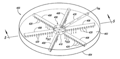
- FIG. 4 is an isometric view and FIG. 5 is a cross-sectional view along line 5 - 5 in FIG. 4 of a plasma unit 400 in accordance with an embodiment of the invention.
- the plasma unit 400 is a window having a high transmissivity to microwave energy or another suitable plasma energy E.
- the plasma unit 400 has a first portion 402 (e.g., top portion), a second portion 404 (e.g., bottom portion), and a chamber 406 with a plurality of discrete conduits 408 extending radially outwardly from a hub 410 .
- the plasma unit 400 further includes a plurality of ports or outlets 420 in the second portion 404 and an inlet passage 430 (see FIG. 4 ).
- the outlets 420 are arranged along the conduits 408 .
- the inlet passage 430 extends from the periphery of the plasma unit 400 into the hub 410 .
- the plasma unit 400 can be formed by drilling the conduits and the inlet passage radially inwardly from the peripheral edge of the plasma unit. The periphery of the plasma unit can then be capped to form the structure shown in FIGS. 4 and 5 .
- the first and second portions 402 and 404 can initially be discrete components connected together at an interface 440 (shown only in FIG. 5 ).
- the conduits 408 in this embodiment are etched or machined into the interior of the first and/or second portions 402 and 404 , and then the first portion 402 is attached to the second portion 404 along the interface 440 .
- the outlets 420 are drilled and/or etched through the second portion 404 to be in fluid communication with the conduits 408 .
- the first and second portions 402 and 404 can be formed from a single panel or body of material that is transmissive to the plasma energy E.
- the first and second portions 402 and 404 can be top and bottom portions of a quartz block.
- only the first portion 402 may be transmissive to the plasma energy E and the second portion 404 may be composed of a different material.
- only the areas of the first portion 402 above the conduits 408 may be formed from a material that is transmissive to the plasma energy E. This embodiment may accordingly have a plurality of discrete windows extending over conduits 408 that have been formed in a block of different material.
- the inlet gas G in flows through the inlet 430 and into the hub 410 .
- the gas then flows through the conduits 408 where it is excited by the plasma energy E to form a plasma.
- the plasma then flows out of the ports 420 in a desired distribution across the workpiece W.
- FIGS. 6A and 6B illustrate another embodiment of a plasma unit 600 for delivering two different gases G 1 and G 2 to the workpiece without mixing the gases G 1 and G 2 in the plasma unit 600 .
- the plasma unit 600 has a first portion 602 configured to face the energy system and a second portion 604 configured to face the workpiece.
- the plasma unit 600 further includes a first chamber 610 having a plurality of first conduits 612 and a plurality of first outlets 614 along the first conduits 612 .
- the plasma unit 600 further includes a second chamber 620 having a plurality of second conduits 622 and a plurality of second outlets 624 along the second conduits 622 .
- each first conduit 612 is not aligned with the second conduits 622 such that the first outlets 614 extend through the plasma unit 600 between the second conduits 622 .
- the first outlets 614 extend to outlet openings underneath the first conduits 612
- the second outlets 624 extend to outlet openings underneath the second conduits 622 .
- the plasma unit 600 is suitable for ALD processes in which pulses of a first precursor gas G 1 flow through the first chamber 610 and pulses of a second precursor gas G 2 flow through the second chamber 620 .
- the pulses can occur simultaneously for CVD process or at different intervals for ALD processes.
- the plasma unit 600 can form a plasma in one or both of the chambers 610 and 620 .
- pulses of a hydrogen plasma formed in the first chamber 610 from H 2 are distributed to the workpiece through the first outlets 614
- pulses of TiCl 4 in the second chamber 620 are distributed to the workpiece W through the second outlets 624 .
- the pulses of the H 2 and TiCl 4 precursors can be separated by a purge gas to form a layer of titanium in an ALD process.
- FIG. 7 is a schematic cross-sectional view illustrating a plasma unit 700 in accordance with another embodiment of the invention.
- the plasma unit 700 has a first portion 702 , a second portion 704 , and a chamber 706 between the first and second portions 702 and 704 .
- the plasma unit 700 further includes a plurality of outlets 708 extending through the second portion 704 .
- the outlets 708 terminate at outlet openings 710 along the bottom surface of the second portion 704 .
- the second portion 704 has a thickness T selected to position the outlet openings 710 from the workpiece W by a desired distance D. It will be appreciated that the distance D is selected according to the desired distribution of the processes gases across the workpiece W.
- the second portion 704 can also have a lateral dimension S to size the array of outlet openings 710 to the size of the workpiece W.
- One advantage of the plasma unit 700 is that different plasma units can be installed in a single processing vessel to provide the desired distribution of process gases to different types of workpieces.
- the thickness T for example, can be adjusted to process workpieces having different types of devices.
- the lateral dimension S can be changed to retrofit a 200 mm chamber to 300 mm chamber. This provides a significant advantage over conventional systems in which the distribution of gases cannot be tailored to accommodate different types of workpieces using the same chamber.
- FIG. 8 illustrates another embodiment of a process unit 800 having a lower portion 810 with a contoured surface 812 .
- the plasma unit 800 further includes a plurality of outlets 820 that terminate along the lower surface 812 at outlet openings 822 .
- the plasma unit 800 provides a different distance between the outlet openings 822 and a workpiece (not shown in FIG. 8 ) to further control the distribution of process gases and/or plasma.
- the surface 812 can have a number of different configurations to provide the desired distribution of process gases across the workpiece.
- FIG. 9 is a schematic cross-sectional view of a plasma unit 900 in accordance with yet another embodiment of the invention.
- the plasma unit 900 includes a first portion 902 , a second portion 904 , and a chamber 906 within the first and second portions 902 and 904 .
- the second portion 904 of the plasma unit 900 includes a plurality of different outlets including a first plurality of holes 920 (shown schematically) and a second plurality of holes 922 (shown schematically).
- the first holes 920 can be arranged in an inner region I r and the plurality of second holes 922 can be arranged in a peripheral region P r .
- the first holes 920 have a different characteristic than the second holes 922 to facilitate different distributions of processing gases across the workpiece.
- the first holes 920 can have a larger diameter or different shape than the second holes 922 .
- the first holes 920 can have a higher density (i.e., occupy more surface area) than the second holes 922 . It will be appreciated that the inverse is possible such that the second holes 922 can be larger and/or have a higher density than the first holes 920 .
- the inner region I r and the peripheral region P r can be discrete regions having a defined boundary. The transition between the inner region I r and the peripheral region P r , however, can change along a continuum.
- FIG. 10 is a schematic cross-sectional view of a plasma vapor processing system 100 a in accordance with another embodiment of the invention.
- Like reference numbers refer to like components in FIGS. 3 and 10 , and thus the description of such components will not be repeated with reference to the processing system 100 a .
- the difference between the processing system 100 shown in FIG. 3 and the processing system 100 a shown in FIG. 10 is that the processing system 100 a has a plasma unit 1060 having a first portion 1062 separate from a second portion 1064 .
- the first portion 1062 can be a window comprising quartz or another suitable material for transmitting the plasma energy E.
- the second portion 1064 is spaced apart from the first portion 1062 to define a chamber 1066 in which the inlet gases G in are injected.
- the sidewalls of the chamber 1066 can accordingly be an interior wall of the processing vessel 120 or a liner within the processing vessel 120 .
- the plasma energy E propagates through the first portion 1062 and generates a plasma from an inlet gas G in in the chamber 1066 .
- the plasma unit 1060 accordingly has a plurality of outlets 1068 in the second portion 1064 to dispense an outlet plasma P out relative to the workpiece W.
- the processing system 100 a is expected to have similar performance characteristics as the processing system 100 shown in FIG. 3 .
Abstract
Description
Claims (4)
Priority Applications (1)
| Application Number | Priority Date | Filing Date | Title |
|---|---|---|---|
| US10/683,424 US7581511B2 (en) | 2003-10-10 | 2003-10-10 | Apparatus and methods for manufacturing microfeatures on workpieces using plasma vapor processes |
Applications Claiming Priority (1)
| Application Number | Priority Date | Filing Date | Title |
|---|---|---|---|
| US10/683,424 US7581511B2 (en) | 2003-10-10 | 2003-10-10 | Apparatus and methods for manufacturing microfeatures on workpieces using plasma vapor processes |
Publications (2)
| Publication Number | Publication Date |
|---|---|
| US20050087302A1 US20050087302A1 (en) | 2005-04-28 |
| US7581511B2 true US7581511B2 (en) | 2009-09-01 |
Family
ID=34520558
Family Applications (1)
| Application Number | Title | Priority Date | Filing Date |
|---|---|---|---|
| US10/683,424 Expired - Fee Related US7581511B2 (en) | 2003-10-10 | 2003-10-10 | Apparatus and methods for manufacturing microfeatures on workpieces using plasma vapor processes |
Country Status (1)
| Country | Link |
|---|---|
| US (1) | US7581511B2 (en) |
Cited By (169)
| Publication number | Priority date | Publication date | Assignee | Title |
|---|---|---|---|---|
| US20080265737A1 (en) * | 2006-07-31 | 2008-10-30 | Worldex Industry & Trading Co., Ltd. | Plasma Chamber Cathode and Outer Ring Made of Silicon Material |
| US20090159001A1 (en) * | 2004-08-11 | 2009-06-25 | Pyung-Yong Um | Shower head of chemical vapor deposition apparatus |
| US20100167551A1 (en) * | 2008-12-30 | 2010-07-01 | Intermolecular Inc. | Dual path gas distribution device |
| US20110151674A1 (en) * | 2009-12-23 | 2011-06-23 | Applied Materials, Inc. | Smooth siconi etch for silicon-containing films |
| US20120135145A1 (en) * | 2009-07-08 | 2012-05-31 | Sung Tae Je | Substrate-processing apparatus and substrate-processing method for selectively inserting diffusion plates |
| US20120237696A1 (en) * | 2011-03-18 | 2012-09-20 | Axcelis Technologies, Inc. | Fluid distribution members and/or assemblies |
| US20130126486A1 (en) * | 2011-11-22 | 2013-05-23 | Ryan Bise | Multi Zone Gas Injection Upper Electrode System |
| CN103392217A (en) * | 2010-12-23 | 2013-11-13 | 六号元素有限公司 | A microwave plasma reactor for manufacturing synthetic diamond material |
| US8679983B2 (en) | 2011-09-01 | 2014-03-25 | Applied Materials, Inc. | Selective suppression of dry-etch rate of materials containing both silicon and nitrogen |
| US8679982B2 (en) | 2011-08-26 | 2014-03-25 | Applied Materials, Inc. | Selective suppression of dry-etch rate of materials containing both silicon and oxygen |
| US8741778B2 (en) | 2010-12-14 | 2014-06-03 | Applied Materials, Inc. | Uniform dry etch in two stages |
| US8765574B2 (en) | 2012-11-09 | 2014-07-01 | Applied Materials, Inc. | Dry etch process |
| US8771536B2 (en) | 2011-08-01 | 2014-07-08 | Applied Materials, Inc. | Dry-etch for silicon-and-carbon-containing films |
| US8771539B2 (en) | 2011-02-22 | 2014-07-08 | Applied Materials, Inc. | Remotely-excited fluorine and water vapor etch |
| US20140202388A1 (en) * | 2008-09-30 | 2014-07-24 | Eugene Technology Co., Ltd. | Shower head unit and chemical vapor deposition apparatus |
| US8801952B1 (en) | 2013-03-07 | 2014-08-12 | Applied Materials, Inc. | Conformal oxide dry etch |
| US8808563B2 (en) | 2011-10-07 | 2014-08-19 | Applied Materials, Inc. | Selective etch of silicon by way of metastable hydrogen termination |
| US8895449B1 (en) | 2013-05-16 | 2014-11-25 | Applied Materials, Inc. | Delicate dry clean |
| US8921234B2 (en) | 2012-12-21 | 2014-12-30 | Applied Materials, Inc. | Selective titanium nitride etching |
| US8927390B2 (en) | 2011-09-26 | 2015-01-06 | Applied Materials, Inc. | Intrench profile |
| US8951429B1 (en) | 2013-10-29 | 2015-02-10 | Applied Materials, Inc. | Tungsten oxide processing |
| US8956980B1 (en) | 2013-09-16 | 2015-02-17 | Applied Materials, Inc. | Selective etch of silicon nitride |
| US8969212B2 (en) | 2012-11-20 | 2015-03-03 | Applied Materials, Inc. | Dry-etch selectivity |
| US8975152B2 (en) | 2011-11-08 | 2015-03-10 | Applied Materials, Inc. | Methods of reducing substrate dislocation during gapfill processing |
| US8980763B2 (en) | 2012-11-30 | 2015-03-17 | Applied Materials, Inc. | Dry-etch for selective tungsten removal |
| US8980764B2 (en) * | 2011-03-14 | 2015-03-17 | Plasma-Therm Llc | Method and apparatus for plasma dicing a semi-conductor wafer |
| US9023732B2 (en) | 2013-03-15 | 2015-05-05 | Applied Materials, Inc. | Processing systems and methods for halide scavenging |
| US9023734B2 (en) | 2012-09-18 | 2015-05-05 | Applied Materials, Inc. | Radical-component oxide etch |
| US9034770B2 (en) | 2012-09-17 | 2015-05-19 | Applied Materials, Inc. | Differential silicon oxide etch |
| US9040422B2 (en) | 2013-03-05 | 2015-05-26 | Applied Materials, Inc. | Selective titanium nitride removal |
| US9064816B2 (en) | 2012-11-30 | 2015-06-23 | Applied Materials, Inc. | Dry-etch for selective oxidation removal |
| US9083182B2 (en) | 2011-11-21 | 2015-07-14 | Lam Research Corporation | Bypass capacitors for high voltage bias power in the mid frequency RF range |
| US20150214009A1 (en) * | 2014-01-25 | 2015-07-30 | Yuri Glukhoy | Showerhead-cooler system of a semiconductor-processing chamber for semiconductor wafers of large area |
| US9111877B2 (en) | 2012-12-18 | 2015-08-18 | Applied Materials, Inc. | Non-local plasma oxide etch |
| US9117855B2 (en) | 2013-12-04 | 2015-08-25 | Applied Materials, Inc. | Polarity control for remote plasma |
| US9114438B2 (en) | 2013-05-21 | 2015-08-25 | Applied Materials, Inc. | Copper residue chamber clean |
| US9136273B1 (en) | 2014-03-21 | 2015-09-15 | Applied Materials, Inc. | Flash gate air gap |
| US9132436B2 (en) | 2012-09-21 | 2015-09-15 | Applied Materials, Inc. | Chemical control features in wafer process equipment |
| US9159606B1 (en) | 2014-07-31 | 2015-10-13 | Applied Materials, Inc. | Metal air gap |
| US9165786B1 (en) | 2014-08-05 | 2015-10-20 | Applied Materials, Inc. | Integrated oxide and nitride recess for better channel contact in 3D architectures |
| US9190293B2 (en) | 2013-12-18 | 2015-11-17 | Applied Materials, Inc. | Even tungsten etch for high aspect ratio trenches |
| US9236265B2 (en) | 2013-11-04 | 2016-01-12 | Applied Materials, Inc. | Silicon germanium processing |
| US9245762B2 (en) | 2013-12-02 | 2016-01-26 | Applied Materials, Inc. | Procedure for etch rate consistency |
| US9263278B2 (en) | 2013-12-17 | 2016-02-16 | Applied Materials, Inc. | Dopant etch selectivity control |
| US9269590B2 (en) | 2014-04-07 | 2016-02-23 | Applied Materials, Inc. | Spacer formation |
| US9287095B2 (en) | 2013-12-17 | 2016-03-15 | Applied Materials, Inc. | Semiconductor system assemblies and methods of operation |
| US9287134B2 (en) | 2014-01-17 | 2016-03-15 | Applied Materials, Inc. | Titanium oxide etch |
| US9293568B2 (en) | 2014-01-27 | 2016-03-22 | Applied Materials, Inc. | Method of fin patterning |
| US9299537B2 (en) | 2014-03-20 | 2016-03-29 | Applied Materials, Inc. | Radial waveguide systems and methods for post-match control of microwaves |
| US9299583B1 (en) | 2014-12-05 | 2016-03-29 | Applied Materials, Inc. | Aluminum oxide selective etch |
| US9299538B2 (en) | 2014-03-20 | 2016-03-29 | Applied Materials, Inc. | Radial waveguide systems and methods for post-match control of microwaves |
| US9299582B2 (en) | 2013-11-12 | 2016-03-29 | Applied Materials, Inc. | Selective etch for metal-containing materials |
| US9299575B2 (en) | 2014-03-17 | 2016-03-29 | Applied Materials, Inc. | Gas-phase tungsten etch |
| US9309598B2 (en) | 2014-05-28 | 2016-04-12 | Applied Materials, Inc. | Oxide and metal removal |
| US9324576B2 (en) | 2010-05-27 | 2016-04-26 | Applied Materials, Inc. | Selective etch for silicon films |
| US9343272B1 (en) | 2015-01-08 | 2016-05-17 | Applied Materials, Inc. | Self-aligned process |
| US9349605B1 (en) | 2015-08-07 | 2016-05-24 | Applied Materials, Inc. | Oxide etch selectivity systems and methods |
| US9355862B2 (en) | 2014-09-24 | 2016-05-31 | Applied Materials, Inc. | Fluorine-based hardmask removal |
| US9355856B2 (en) | 2014-09-12 | 2016-05-31 | Applied Materials, Inc. | V trench dry etch |
| US9362130B2 (en) | 2013-03-01 | 2016-06-07 | Applied Materials, Inc. | Enhanced etching processes using remote plasma sources |
| US9368364B2 (en) | 2014-09-24 | 2016-06-14 | Applied Materials, Inc. | Silicon etch process with tunable selectivity to SiO2 and other materials |
| US9373517B2 (en) | 2012-08-02 | 2016-06-21 | Applied Materials, Inc. | Semiconductor processing with DC assisted RF power for improved control |
| US9373522B1 (en) | 2015-01-22 | 2016-06-21 | Applied Mateials, Inc. | Titanium nitride removal |
| US9378978B2 (en) | 2014-07-31 | 2016-06-28 | Applied Materials, Inc. | Integrated oxide recess and floating gate fin trimming |
| US9378969B2 (en) | 2014-06-19 | 2016-06-28 | Applied Materials, Inc. | Low temperature gas-phase carbon removal |
| US9385028B2 (en) | 2014-02-03 | 2016-07-05 | Applied Materials, Inc. | Air gap process |
| US9390937B2 (en) | 2012-09-20 | 2016-07-12 | Applied Materials, Inc. | Silicon-carbon-nitride selective etch |
| US9396989B2 (en) | 2014-01-27 | 2016-07-19 | Applied Materials, Inc. | Air gaps between copper lines |
| US9396908B2 (en) | 2011-11-22 | 2016-07-19 | Lam Research Corporation | Systems and methods for controlling a plasma edge region |
| US9406523B2 (en) | 2014-06-19 | 2016-08-02 | Applied Materials, Inc. | Highly selective doped oxide removal method |
| US9425058B2 (en) | 2014-07-24 | 2016-08-23 | Applied Materials, Inc. | Simplified litho-etch-litho-etch process |
| US9449846B2 (en) | 2015-01-28 | 2016-09-20 | Applied Materials, Inc. | Vertical gate separation |
| US9478432B2 (en) | 2014-09-25 | 2016-10-25 | Applied Materials, Inc. | Silicon oxide selective removal |
| US9496167B2 (en) | 2014-07-31 | 2016-11-15 | Applied Materials, Inc. | Integrated bit-line airgap formation and gate stack post clean |
| US9493879B2 (en) | 2013-07-12 | 2016-11-15 | Applied Materials, Inc. | Selective sputtering for pattern transfer |
| US9499898B2 (en) | 2014-03-03 | 2016-11-22 | Applied Materials, Inc. | Layered thin film heater and method of fabrication |
| US9502258B2 (en) | 2014-12-23 | 2016-11-22 | Applied Materials, Inc. | Anisotropic gap etch |
| US9508530B2 (en) | 2011-11-21 | 2016-11-29 | Lam Research Corporation | Plasma processing chamber with flexible symmetric RF return strap |
| US9553102B2 (en) | 2014-08-19 | 2017-01-24 | Applied Materials, Inc. | Tungsten separation |
| US9576809B2 (en) | 2013-11-04 | 2017-02-21 | Applied Materials, Inc. | Etch suppression with germanium |
| US9659753B2 (en) | 2014-08-07 | 2017-05-23 | Applied Materials, Inc. | Grooved insulator to reduce leakage current |
| US9691645B2 (en) | 2015-08-06 | 2017-06-27 | Applied Materials, Inc. | Bolted wafer chuck thermal management systems and methods for wafer processing systems |
| US9721789B1 (en) | 2016-10-04 | 2017-08-01 | Applied Materials, Inc. | Saving ion-damaged spacers |
| US9728437B2 (en) | 2015-02-03 | 2017-08-08 | Applied Materials, Inc. | High temperature chuck for plasma processing systems |
| US9741593B2 (en) | 2015-08-06 | 2017-08-22 | Applied Materials, Inc. | Thermal management systems and methods for wafer processing systems |
| US9768034B1 (en) | 2016-11-11 | 2017-09-19 | Applied Materials, Inc. | Removal methods for high aspect ratio structures |
| US9773648B2 (en) | 2013-08-30 | 2017-09-26 | Applied Materials, Inc. | Dual discharge modes operation for remote plasma |
| US9842744B2 (en) | 2011-03-14 | 2017-12-12 | Applied Materials, Inc. | Methods for etch of SiN films |
| US9847289B2 (en) | 2014-05-30 | 2017-12-19 | Applied Materials, Inc. | Protective via cap for improved interconnect performance |
| US9865484B1 (en) | 2016-06-29 | 2018-01-09 | Applied Materials, Inc. | Selective etch using material modification and RF pulsing |
| US9881805B2 (en) | 2015-03-02 | 2018-01-30 | Applied Materials, Inc. | Silicon selective removal |
| US9885117B2 (en) | 2014-03-31 | 2018-02-06 | Applied Materials, Inc. | Conditioned semiconductor system parts |
| US9934942B1 (en) | 2016-10-04 | 2018-04-03 | Applied Materials, Inc. | Chamber with flow-through source |
| US9947549B1 (en) | 2016-10-10 | 2018-04-17 | Applied Materials, Inc. | Cobalt-containing material removal |
| US10026621B2 (en) | 2016-11-14 | 2018-07-17 | Applied Materials, Inc. | SiN spacer profile patterning |
| US10043674B1 (en) | 2017-08-04 | 2018-08-07 | Applied Materials, Inc. | Germanium etching systems and methods |
| US10043684B1 (en) | 2017-02-06 | 2018-08-07 | Applied Materials, Inc. | Self-limiting atomic thermal etching systems and methods |
| US10049891B1 (en) | 2017-05-31 | 2018-08-14 | Applied Materials, Inc. | Selective in situ cobalt residue removal |
| US10062579B2 (en) | 2016-10-07 | 2018-08-28 | Applied Materials, Inc. | Selective SiN lateral recess |
| US10062587B2 (en) | 2012-07-18 | 2018-08-28 | Applied Materials, Inc. | Pedestal with multi-zone temperature control and multiple purge capabilities |
| US10062575B2 (en) | 2016-09-09 | 2018-08-28 | Applied Materials, Inc. | Poly directional etch by oxidation |
| US10062585B2 (en) | 2016-10-04 | 2018-08-28 | Applied Materials, Inc. | Oxygen compatible plasma source |
| US10062578B2 (en) | 2011-03-14 | 2018-08-28 | Applied Materials, Inc. | Methods for etch of metal and metal-oxide films |
| US10065918B2 (en) | 2013-07-09 | 2018-09-04 | Biosynthetic Technologies, Llc | Polyol estolides and methods of making and using the same |
| US10128086B1 (en) | 2017-10-24 | 2018-11-13 | Applied Materials, Inc. | Silicon pretreatment for nitride removal |
| US10163696B2 (en) | 2016-11-11 | 2018-12-25 | Applied Materials, Inc. | Selective cobalt removal for bottom up gapfill |
| US10170336B1 (en) | 2017-08-04 | 2019-01-01 | Applied Materials, Inc. | Methods for anisotropic control of selective silicon removal |
| US10170282B2 (en) | 2013-03-08 | 2019-01-01 | Applied Materials, Inc. | Insulated semiconductor faceplate designs |
| US10224210B2 (en) | 2014-12-09 | 2019-03-05 | Applied Materials, Inc. | Plasma processing system with direct outlet toroidal plasma source |
| US10242908B2 (en) | 2016-11-14 | 2019-03-26 | Applied Materials, Inc. | Airgap formation with damage-free copper |
| US10256112B1 (en) | 2017-12-08 | 2019-04-09 | Applied Materials, Inc. | Selective tungsten removal |
| US10256079B2 (en) | 2013-02-08 | 2019-04-09 | Applied Materials, Inc. | Semiconductor processing systems having multiple plasma configurations |
| US10283321B2 (en) | 2011-01-18 | 2019-05-07 | Applied Materials, Inc. | Semiconductor processing system and methods using capacitively coupled plasma |
| US10283324B1 (en) | 2017-10-24 | 2019-05-07 | Applied Materials, Inc. | Oxygen treatment for nitride etching |
| US10297458B2 (en) | 2017-08-07 | 2019-05-21 | Applied Materials, Inc. | Process window widening using coated parts in plasma etch processes |
| US10319739B2 (en) | 2017-02-08 | 2019-06-11 | Applied Materials, Inc. | Accommodating imperfectly aligned memory holes |
| US10319649B2 (en) | 2017-04-11 | 2019-06-11 | Applied Materials, Inc. | Optical emission spectroscopy (OES) for remote plasma monitoring |
| US10319600B1 (en) | 2018-03-12 | 2019-06-11 | Applied Materials, Inc. | Thermal silicon etch |
| US10354889B2 (en) | 2017-07-17 | 2019-07-16 | Applied Materials, Inc. | Non-halogen etching of silicon-containing materials |
| US10403507B2 (en) | 2017-02-03 | 2019-09-03 | Applied Materials, Inc. | Shaped etch profile with oxidation |
| US10431429B2 (en) | 2017-02-03 | 2019-10-01 | Applied Materials, Inc. | Systems and methods for radial and azimuthal control of plasma uniformity |
| US10468267B2 (en) | 2017-05-31 | 2019-11-05 | Applied Materials, Inc. | Water-free etching methods |
| US10490406B2 (en) | 2018-04-10 | 2019-11-26 | Appled Materials, Inc. | Systems and methods for material breakthrough |
| US10490418B2 (en) | 2014-10-14 | 2019-11-26 | Applied Materials, Inc. | Systems and methods for internal surface conditioning assessment in plasma processing equipment |
| US10497573B2 (en) | 2018-03-13 | 2019-12-03 | Applied Materials, Inc. | Selective atomic layer etching of semiconductor materials |
| US10504700B2 (en) | 2015-08-27 | 2019-12-10 | Applied Materials, Inc. | Plasma etching systems and methods with secondary plasma injection |
| US10504754B2 (en) | 2016-05-19 | 2019-12-10 | Applied Materials, Inc. | Systems and methods for improved semiconductor etching and component protection |
| US10522371B2 (en) | 2016-05-19 | 2019-12-31 | Applied Materials, Inc. | Systems and methods for improved semiconductor etching and component protection |
| US10541184B2 (en) | 2017-07-11 | 2020-01-21 | Applied Materials, Inc. | Optical emission spectroscopic techniques for monitoring etching |
| US10541246B2 (en) | 2017-06-26 | 2020-01-21 | Applied Materials, Inc. | 3D flash memory cells which discourage cross-cell electrical tunneling |
| US10546729B2 (en) | 2016-10-04 | 2020-01-28 | Applied Materials, Inc. | Dual-channel showerhead with improved profile |
| US10566206B2 (en) | 2016-12-27 | 2020-02-18 | Applied Materials, Inc. | Systems and methods for anisotropic material breakthrough |
| US10573527B2 (en) | 2018-04-06 | 2020-02-25 | Applied Materials, Inc. | Gas-phase selective etching systems and methods |
| US10573496B2 (en) | 2014-12-09 | 2020-02-25 | Applied Materials, Inc. | Direct outlet toroidal plasma source |
| US10586686B2 (en) | 2011-11-22 | 2020-03-10 | Law Research Corporation | Peripheral RF feed and symmetric RF return for symmetric RF delivery |
| US10593560B2 (en) | 2018-03-01 | 2020-03-17 | Applied Materials, Inc. | Magnetic induction plasma source for semiconductor processes and equipment |
| US10593523B2 (en) | 2014-10-14 | 2020-03-17 | Applied Materials, Inc. | Systems and methods for internal surface conditioning in plasma processing equipment |
| US10615047B2 (en) | 2018-02-28 | 2020-04-07 | Applied Materials, Inc. | Systems and methods to form airgaps |
| US10629473B2 (en) | 2016-09-09 | 2020-04-21 | Applied Materials, Inc. | Footing removal for nitride spacer |
| US10672642B2 (en) | 2018-07-24 | 2020-06-02 | Applied Materials, Inc. | Systems and methods for pedestal configuration |
| US10679870B2 (en) | 2018-02-15 | 2020-06-09 | Applied Materials, Inc. | Semiconductor processing chamber multistage mixing apparatus |
| US10699879B2 (en) | 2018-04-17 | 2020-06-30 | Applied Materials, Inc. | Two piece electrode assembly with gap for plasma control |
| US10727080B2 (en) | 2017-07-07 | 2020-07-28 | Applied Materials, Inc. | Tantalum-containing material removal |
| US10755941B2 (en) | 2018-07-06 | 2020-08-25 | Applied Materials, Inc. | Self-limiting selective etching systems and methods |
| US10854426B2 (en) | 2018-01-08 | 2020-12-01 | Applied Materials, Inc. | Metal recess for semiconductor structures |
| US10872778B2 (en) | 2018-07-06 | 2020-12-22 | Applied Materials, Inc. | Systems and methods utilizing solid-phase etchants |
| US10886137B2 (en) | 2018-04-30 | 2021-01-05 | Applied Materials, Inc. | Selective nitride removal |
| US10892198B2 (en) | 2018-09-14 | 2021-01-12 | Applied Materials, Inc. | Systems and methods for improved performance in semiconductor processing |
| US10903054B2 (en) | 2017-12-19 | 2021-01-26 | Applied Materials, Inc. | Multi-zone gas distribution systems and methods |
| US10920320B2 (en) | 2017-06-16 | 2021-02-16 | Applied Materials, Inc. | Plasma health determination in semiconductor substrate processing reactors |
| US10920319B2 (en) | 2019-01-11 | 2021-02-16 | Applied Materials, Inc. | Ceramic showerheads with conductive electrodes |
| US10943834B2 (en) | 2017-03-13 | 2021-03-09 | Applied Materials, Inc. | Replacement contact process |
| US10964512B2 (en) | 2018-02-15 | 2021-03-30 | Applied Materials, Inc. | Semiconductor processing chamber multistage mixing apparatus and methods |
| US11049755B2 (en) | 2018-09-14 | 2021-06-29 | Applied Materials, Inc. | Semiconductor substrate supports with embedded RF shield |
| US11062887B2 (en) | 2018-09-17 | 2021-07-13 | Applied Materials, Inc. | High temperature RF heater pedestals |
| US11121002B2 (en) | 2018-10-24 | 2021-09-14 | Applied Materials, Inc. | Systems and methods for etching metals and metal derivatives |
| US11239061B2 (en) | 2014-11-26 | 2022-02-01 | Applied Materials, Inc. | Methods and systems to enhance process uniformity |
| US11257693B2 (en) | 2015-01-09 | 2022-02-22 | Applied Materials, Inc. | Methods and systems to improve pedestal temperature control |
| US11276559B2 (en) | 2017-05-17 | 2022-03-15 | Applied Materials, Inc. | Semiconductor processing chamber for multiple precursor flow |
| US11276590B2 (en) | 2017-05-17 | 2022-03-15 | Applied Materials, Inc. | Multi-zone semiconductor substrate supports |
| US11286565B2 (en) * | 2018-12-13 | 2022-03-29 | Xia Tai Xin Semiconductor (Qing Dao) Ltd. | Apparatus and method for semiconductor fabrication |
| US11328909B2 (en) | 2017-12-22 | 2022-05-10 | Applied Materials, Inc. | Chamber conditioning and removal processes |
| US11332827B2 (en) * | 2019-03-27 | 2022-05-17 | Applied Materials, Inc. | Gas distribution plate with high aspect ratio holes and a high hole density |
| US11417534B2 (en) | 2018-09-21 | 2022-08-16 | Applied Materials, Inc. | Selective material removal |
| US11437242B2 (en) | 2018-11-27 | 2022-09-06 | Applied Materials, Inc. | Selective removal of silicon-containing materials |
| US11594428B2 (en) | 2015-02-03 | 2023-02-28 | Applied Materials, Inc. | Low temperature chuck for plasma processing systems |
| US11594400B2 (en) * | 2011-11-23 | 2023-02-28 | Lam Research Corporation | Multi zone gas injection upper electrode system |
| US11682560B2 (en) | 2018-10-11 | 2023-06-20 | Applied Materials, Inc. | Systems and methods for hafnium-containing film removal |
| US11721527B2 (en) | 2019-01-07 | 2023-08-08 | Applied Materials, Inc. | Processing chamber mixing systems |
Families Citing this family (18)
| Publication number | Priority date | Publication date | Assignee | Title |
|---|---|---|---|---|
| US6926775B2 (en) * | 2003-02-11 | 2005-08-09 | Micron Technology, Inc. | Reactors with isolated gas connectors and methods for depositing materials onto micro-device workpieces |
| US7422635B2 (en) * | 2003-08-28 | 2008-09-09 | Micron Technology, Inc. | Methods and apparatus for processing microfeature workpieces, e.g., for depositing materials on microfeature workpieces |
| US7323231B2 (en) * | 2003-10-09 | 2008-01-29 | Micron Technology, Inc. | Apparatus and methods for plasma vapor deposition processes |
| US7258892B2 (en) | 2003-12-10 | 2007-08-21 | Micron Technology, Inc. | Methods and systems for controlling temperature during microfeature workpiece processing, e.g., CVD deposition |
| US7906393B2 (en) | 2004-01-28 | 2011-03-15 | Micron Technology, Inc. | Methods for forming small-scale capacitor structures |
| US8133554B2 (en) | 2004-05-06 | 2012-03-13 | Micron Technology, Inc. | Methods for depositing material onto microfeature workpieces in reaction chambers and systems for depositing materials onto microfeature workpieces |
| US7699932B2 (en) | 2004-06-02 | 2010-04-20 | Micron Technology, Inc. | Reactors, systems and methods for depositing thin films onto microfeature workpieces |
| US8349128B2 (en) * | 2004-06-30 | 2013-01-08 | Applied Materials, Inc. | Method and apparatus for stable plasma processing |
| US20060000802A1 (en) * | 2004-06-30 | 2006-01-05 | Ajay Kumar | Method and apparatus for photomask plasma etching |
| US20060237138A1 (en) * | 2005-04-26 | 2006-10-26 | Micron Technology, Inc. | Apparatuses and methods for supporting microelectronic devices during plasma-based fabrication processes |
| JPWO2007049595A1 (en) * | 2005-10-25 | 2009-04-30 | 日本碍子株式会社 | Sterilization sterilizer |
| JP5068458B2 (en) * | 2006-01-18 | 2012-11-07 | 東京エレクトロン株式会社 | Plasma processing apparatus and plasma processing method |
| US7909961B2 (en) * | 2006-10-30 | 2011-03-22 | Applied Materials, Inc. | Method and apparatus for photomask plasma etching |
| US7943005B2 (en) | 2006-10-30 | 2011-05-17 | Applied Materials, Inc. | Method and apparatus for photomask plasma etching |
| US8375890B2 (en) * | 2007-03-19 | 2013-02-19 | Micron Technology, Inc. | Apparatus and methods for capacitively coupled plasma vapor processing of semiconductor wafers |
| US9105705B2 (en) * | 2011-03-14 | 2015-08-11 | Plasma-Therm Llc | Method and apparatus for plasma dicing a semi-conductor wafer |
| US9245717B2 (en) | 2011-05-31 | 2016-01-26 | Lam Research Corporation | Gas distribution system for ceramic showerhead of plasma etch reactor |
| JP6219179B2 (en) * | 2014-01-20 | 2017-10-25 | 東京エレクトロン株式会社 | Plasma processing equipment |
Citations (112)
| Publication number | Priority date | Publication date | Assignee | Title |
|---|---|---|---|---|
| US127031A (en) | 1872-05-21 | Improvement in apparatus for carbureting air | ||
| US131943A (en) | 1872-10-08 | Improvement in carbureters for air and gas | ||
| US579269A (en) | 1897-03-23 | Roller-bearing | ||
| US1741519A (en) | 1926-12-10 | 1929-12-31 | Universal Oil Prod Co | Dephlegmator or fractionating column |
| US2508500A (en) | 1942-05-23 | 1950-05-23 | Hartford Nat Bank & Trust Co | Apparatus for applying metal coatings on insulators |
| USRE24291E (en) | 1957-03-19 | Device for introducing atomized liquid into gas under pressure | ||
| US3522836A (en) | 1966-07-06 | 1970-08-04 | Battelle Development Corp | Method of manufacturing wire and the like |
| US3618919A (en) | 1969-11-03 | 1971-11-09 | Btu Eng Corp | Adjustable heat and gas barrier |
| US3620934A (en) | 1966-08-08 | 1971-11-16 | Fer Blanc Sarl Centre Rech Du | Method of electrolytic tinning sheet steel |
| US3630881A (en) | 1970-01-22 | 1971-12-28 | Ibm | Cathode-target assembly for rf sputtering apparatus |
| US3630769A (en) | 1968-04-24 | 1971-12-28 | Plessey Co Ltd | PRODUCTION OF VAPOR-DEPOSITED Nb{11 B{11 Sn CONDUCTOR MATERIAL |
| US3634212A (en) | 1970-05-06 | 1972-01-11 | M & T Chemicals Inc | Electrodeposition of bright acid tin and electrolytes therefor |
| US3744771A (en) | 1970-07-20 | 1973-07-10 | Ahldea Corp | Disposable liquid entraining system |
| US3945804A (en) | 1972-09-06 | 1976-03-23 | Sun Ventures, Inc. | Ammoxidation apparatus |
| US4018949A (en) | 1976-01-12 | 1977-04-19 | Ford Motor Company | Selective tin deposition onto aluminum piston skirt areas |
| US4022928A (en) | 1975-05-22 | 1977-05-10 | Piwcyzk Bernhard P | Vacuum deposition methods and masking structure |
| US4098923A (en) | 1976-06-07 | 1978-07-04 | Motorola, Inc. | Pyrolytic deposition of silicon dioxide on semiconductors using a shrouded boat |
| US4242182A (en) | 1978-07-21 | 1980-12-30 | Francine Popescu | Bright tin electroplating bath |
| US4242370A (en) | 1978-03-17 | 1980-12-30 | Abdalla Mohamed I | Method of manufacturing thin film electroluminescent devices |
| US4269625A (en) | 1978-12-04 | 1981-05-26 | U.S. Philips Corporation | Bath for electroless depositing tin on substrates |
| US4289061A (en) | 1977-10-03 | 1981-09-15 | Hooker Chemicals & Plastics Corp. | Device and assembly for mounting parts |
| US4313783A (en) | 1980-05-19 | 1982-02-02 | Branson International Plasma Corporation | Computer controlled system for processing semiconductor wafers |
| US4388342A (en) | 1979-05-29 | 1983-06-14 | Hitachi, Ltd. | Method for chemical vapor deposition |
| US4397753A (en) | 1982-09-20 | 1983-08-09 | Circuit Chemistry Corporation | Solder stripping solution |
| US4436674A (en) | 1981-07-30 | 1984-03-13 | J.C. Schumacher Co. | Vapor mass flow control system |
| US4438724A (en) | 1982-08-13 | 1984-03-27 | Energy Conversion Devices, Inc. | Grooved gas gate |
| US4469801A (en) | 1980-09-04 | 1984-09-04 | Toshio Hirai | Titanium-containing silicon nitride film bodies and a method of producing the same |
| US4492716A (en) | 1979-08-16 | 1985-01-08 | Shunpei Yamazaki | Method of making non-crystalline semiconductor layer |
| US4509456A (en) | 1981-07-28 | 1985-04-09 | Veb Zentrum Fur Forschung Und Technologie Mikroelektronik | Apparatus for guiding gas for LP CVD processes in a tube reactor |
| US4545136A (en) | 1981-03-16 | 1985-10-08 | Sovonics Solar Systems | Isolation valve |
| US4590042A (en) | 1984-12-24 | 1986-05-20 | Tegal Corporation | Plasma reactor having slotted manifold |
| US4593644A (en) | 1983-10-26 | 1986-06-10 | Rca Corporation | Continuous in-line deposition system |
| US4595399A (en) | 1984-11-05 | 1986-06-17 | The United States Of America As Represented By The Administrator Of The National Aeronautics And Space Administration | Nebulization reflux concentrator |
| US4615904A (en) | 1982-06-01 | 1986-10-07 | Massachusetts Institute Of Technology | Maskless growth of patterned films |
| US4681777A (en) | 1986-05-05 | 1987-07-21 | Engelken Robert D | Method for electroless and vapor deposition of thin films of three tin sulfide phases on conductive and nonconductive substrates |
| US4721629A (en) | 1983-06-21 | 1988-01-26 | Sanyo Electric Co., Ltd. | Method of manufacturing photovoltaic device |
| US4738295A (en) | 1985-04-02 | 1988-04-19 | Genser Hans G | Method and apparatus for evaporating a fluid in a rotating vacuum evaporation system |
| US4780178A (en) | 1982-10-15 | 1988-10-25 | Yamoto Scientific Co. Ltd. | Rotary evaporator with control system |
| US4821302A (en) | 1988-02-29 | 1989-04-11 | The United States Of America As Represented By The Secretary Of The Navy | Method and apparatus for transient unit cell measurement |
| US4826579A (en) | 1982-06-25 | 1989-05-02 | Cel Systems Corporation | Electrolytic preparation of tin and other metals |
| US4832115A (en) | 1986-07-09 | 1989-05-23 | Albers Technologies Corporation | Method and apparatus for simultaneous heat and mass transfer |
| US4871417A (en) | 1986-07-04 | 1989-10-03 | Dainippon Screen Mfg. Co., Ltd. | Method and apparatus for surface treating of substrates |
| US4894132A (en) | 1987-10-21 | 1990-01-16 | Mitsubishi Denki Kabushiki Kaisha | Sputtering method and apparatus |
| US4911638A (en) | 1989-05-18 | 1990-03-27 | Direction Incorporated | Controlled diffusion environment capsule and system |
| US4923715A (en) | 1986-03-31 | 1990-05-08 | Kabushiki Kaisha Toshiba | Method of forming thin film by chemical vapor deposition |
| US4948979A (en) | 1987-12-21 | 1990-08-14 | Kabushiki Kaisha Toshiba | Vacuum device for handling workpieces |
| US4949669A (en) | 1988-12-20 | 1990-08-21 | Texas Instruments Incorporated | Gas flow systems in CCVD reactors |
| US4962057A (en) | 1988-10-13 | 1990-10-09 | Xerox Corporation | Method of in situ photo induced evaporation enhancement of compound thin films during or after epitaxial growth |
| US4966646A (en) | 1986-09-24 | 1990-10-30 | Board Of Trustees Of Leland Stanford University | Method of making an integrated, microminiature electric-to-fluidic valve |
| US4977106A (en) | 1990-05-01 | 1990-12-11 | Texas Instruments Incorporated | Tin chemical vapor deposition using TiCl4 and SiH4 |
| US4988879A (en) | 1987-02-24 | 1991-01-29 | The Board Of Trustees Of The Leland Stanford Junior College | Apparatus and method for laser desorption of molecules for quantitation |
| US5015330A (en) | 1989-02-28 | 1991-05-14 | Kabushiki Kaisha Toshiba | Film forming method and film forming device |
| US5017404A (en) | 1988-09-06 | 1991-05-21 | Schott Glaswerke | Plasma CVD process using a plurality of overlapping plasma columns |
| US5020476A (en) | 1990-04-17 | 1991-06-04 | Ds Research, Inc. | Distributed source assembly |
| US5062446A (en) | 1991-01-07 | 1991-11-05 | Sematech, Inc. | Intelligent mass flow controller |
| US5065697A (en) | 1989-07-28 | 1991-11-19 | Matsushita Electric Industrial Co., Ltd. | Laser sputtering apparatus |
| US5076205A (en) | 1989-01-06 | 1991-12-31 | General Signal Corporation | Modular vapor processor system |
| US5091207A (en) | 1989-07-20 | 1992-02-25 | Fujitsu Limited | Process and apparatus for chemical vapor deposition |
| US5090985A (en) | 1989-10-17 | 1992-02-25 | Libbey-Owens-Ford Co. | Method for preparing vaporized reactants for chemical vapor deposition |
| US5131752A (en) | 1990-06-28 | 1992-07-21 | Tamarack Scientific Co., Inc. | Method for film thickness endpoint control |
| US5136975A (en) | 1990-06-21 | 1992-08-11 | Watkins-Johnson Company | Injector and method for delivering gaseous chemicals to a surface |
| US5139606A (en) | 1989-12-05 | 1992-08-18 | Massachusetts Institute Of Technology | Laser bilayer etching of GaAs surfaces |
| US5172849A (en) | 1991-09-25 | 1992-12-22 | General Motors Corporation | Method and apparatus for convection brazing of aluminum heat exchangers |
| US5178683A (en) | 1990-03-30 | 1993-01-12 | New Japan Radio Co., Ltd. | Microwave plasma cvd apparatus |
| US5200023A (en) | 1991-08-30 | 1993-04-06 | International Business Machines Corp. | Infrared thermographic method and apparatus for etch process monitoring and control |
| US5223113A (en) | 1990-07-20 | 1993-06-29 | Tokyo Electron Limited | Apparatus for forming reduced pressure and for processing object |
| US5232749A (en) | 1991-04-30 | 1993-08-03 | Micron Technology, Inc. | Formation of self-limiting films by photoemission induced vapor deposition |
| US5248527A (en) | 1991-03-01 | 1993-09-28 | C. Uyemura And Company, Limited | Process for electroless plating tin, lead or tin-lead alloy |
| US5286296A (en) | 1991-01-10 | 1994-02-15 | Sony Corporation | Multi-chamber wafer process equipment having plural, physically communicating transfer means |
| US5325020A (en) * | 1990-09-28 | 1994-06-28 | Abtox, Inc. | Circular waveguide plasma microwave sterilizer apparatus |
| US5364219A (en) | 1991-06-24 | 1994-11-15 | Tdk Corporation | Apparatus for clean transfer of objects |
| US5366557A (en) | 1990-06-18 | 1994-11-22 | At&T Bell Laboratories | Method and apparatus for forming integrated circuit layers |
| US5372837A (en) | 1990-05-30 | 1994-12-13 | Sharp Kabushiki Kaisha | Method of manufacturing thin film EL device utilizing a shutter |
| US5377429A (en) | 1993-04-19 | 1995-01-03 | Micron Semiconductor, Inc. | Method and appartus for subliming precursors |
| US5378502A (en) | 1992-09-09 | 1995-01-03 | U.S. Philips Corporation | Method of chemically modifying a surface in accordance with a pattern |
| US5380396A (en) | 1991-05-30 | 1995-01-10 | Hitachi, Ltd. | Valve and semiconductor fabricating equipment using the same |
| US5409129A (en) | 1990-12-28 | 1995-04-25 | Hokkai Can Co., Ltd. | Welded cans |
| US5418180A (en) | 1994-06-14 | 1995-05-23 | Micron Semiconductor, Inc. | Process for fabricating storage capacitor structures using CVD tin on hemispherical grain silicon |
| US5421957A (en) | 1993-07-30 | 1995-06-06 | Applied Materials, Inc. | Low temperature etching in cold-wall CVD systems |
| US5427666A (en) | 1993-09-09 | 1995-06-27 | Applied Materials, Inc. | Method for in-situ cleaning a Ti target in a Ti + TiN coating process |
| US5432015A (en) | 1992-05-08 | 1995-07-11 | Westaim Technologies, Inc. | Electroluminescent laminate with thick film dielectric |
| US5433835A (en) | 1993-11-24 | 1995-07-18 | Applied Materials, Inc. | Sputtering device and target with cover to hold cooling fluid |
| US5433787A (en) * | 1991-12-12 | 1995-07-18 | Canon Kabushiki Kaisha | Apparatus for forming deposited film including light transmissive diffusion plate |
| US5445491A (en) | 1991-08-27 | 1995-08-29 | Toshiba Kikai Kabushiki Kaisha | Method for multichamber sheet-after-sheet type treatment |
| US5453124A (en) | 1992-12-30 | 1995-09-26 | Texas Instruments Incorporated | Programmable multizone gas injector for single-wafer semiconductor processing equipment |
| US5474612A (en) | 1990-03-19 | 1995-12-12 | Kabushiki Kaisha Toshiba | Vapor-phase deposition apparatus and vapor-phase deposition method |
| US5477623A (en) | 1992-11-25 | 1995-12-26 | Matsushita Electric Industrial Co., Ltd. | Drying apparatus |
| US5480818A (en) | 1992-02-10 | 1996-01-02 | Fujitsu Limited | Method for forming a film and method for manufacturing a thin film transistor |
| US5496410A (en) | 1992-03-10 | 1996-03-05 | Hitachi, Ltd. | Plasma processing apparatus and method of processing substrates by using same apparatus |
| US5498292A (en) | 1994-06-16 | 1996-03-12 | Kishimoto Sangyo Co., Ltd. | Heating device used for a gas phase growing mechanism or heat treatment mechanism |
| US5500256A (en) | 1994-08-16 | 1996-03-19 | Fujitsu Limited | Dry process apparatus using plural kinds of gas |
| US5505986A (en) | 1994-02-14 | 1996-04-09 | Planar Systems, Inc. | Multi-source reactive deposition process for the preparation of blue light emitting phosphor layers for AC TFEL devices |
| US5522934A (en) | 1994-04-26 | 1996-06-04 | Tokyo Electron Limited | Plasma processing apparatus using vertical gas inlets one on top of another |
| US5527396A (en) | 1992-06-30 | 1996-06-18 | Canon Kabushiki Kaisha | Deposited film forming apparatus |
| US5532190A (en) | 1994-05-26 | 1996-07-02 | U.S. Philips Corporation | Plasma treatment method in electronic device manufacture |
| US5536317A (en) | 1995-10-27 | 1996-07-16 | Specialty Coating Systems, Inc. | Parylene deposition apparatus including a quartz crystal thickness/rate controller |
| US5558717A (en) | 1994-11-30 | 1996-09-24 | Applied Materials | CVD Processing chamber |
| US5562800A (en) | 1993-09-20 | 1996-10-08 | Hitachi, Ltd. | Wafer transport method |
| US5569350A (en) | 1994-03-18 | 1996-10-29 | Anelva Corporation | Mechanism and method for mechanically removing a substrate |
| US5575883A (en) * | 1993-07-09 | 1996-11-19 | Fujitsu Limited | Apparatus and process for fabricating semiconductor devices |
| US5589110A (en) | 1992-11-20 | 1996-12-31 | Mitsubishi Electric Corp | Container for liquid metal organic compound |
| US5589002A (en) | 1994-03-24 | 1996-12-31 | Applied Materials, Inc. | Gas distribution plate for semiconductor wafer processing apparatus with means for inhibiting arcing |
| US5866986A (en) * | 1996-08-05 | 1999-02-02 | Integrated Electronic Innovations, Inc. | Microwave gas phase plasma source |
| US5961775A (en) * | 1987-08-19 | 1999-10-05 | Fujitsu Limited | Apparatus for removing organic resist from semiconductor |
| US5968275A (en) * | 1997-06-25 | 1999-10-19 | Lam Research Corporation | Methods and apparatus for passivating a substrate in a plasma reactor |
| US20020000202A1 (en) * | 2000-06-29 | 2002-01-03 | Katsuhisa Yuda | Remote plasma apparatus for processing sustrate with two types of gases |
| US20020020498A1 (en) * | 2000-05-26 | 2002-02-21 | Tadahiro Ohmi | Plasma processing apparatus and plasma processing method |
| US20030031794A1 (en) * | 1997-12-24 | 2003-02-13 | Kunihiro Tada | Method of forming titanium film by CVD |
| US6656540B2 (en) * | 2000-03-27 | 2003-12-02 | Mitsubishi Heavy Industries, Ltd. | Method for forming metallic film and apparatus for forming the same |
| US6830652B1 (en) * | 1999-05-26 | 2004-12-14 | Tokyo Electron Limited | Microwave plasma processing apparatus |
| US6845734B2 (en) * | 2002-04-11 | 2005-01-25 | Micron Technology, Inc. | Deposition apparatuses configured for utilizing phased microwave radiation |
| US20050217582A1 (en) * | 2001-03-19 | 2005-10-06 | Apex Co., Ltd. | Chemical vapor deposition method |
Family Cites Families (69)
| Publication number | Priority date | Publication date | Assignee | Title |
|---|---|---|---|---|
| JP2703813B2 (en) * | 1989-11-13 | 1998-01-26 | 昭和電工株式会社 | Gas dispersion plate of fluidized bed type gas phase polymerization equipment |
| US5656211A (en) * | 1989-12-22 | 1997-08-12 | Imarx Pharmaceutical Corp. | Apparatus and method for making gas-filled vesicles of optimal size |
| US5716796A (en) * | 1990-01-23 | 1998-02-10 | Medical Devices Corporation | Optical blood hemostatic analysis apparatus and method |
| US5592581A (en) * | 1993-07-19 | 1997-01-07 | Tokyo Electron Kabushiki Kaisha | Heat treatment apparatus |
| FI95421C (en) * | 1993-12-23 | 1996-01-25 | Heikki Ihantola | Device and method for treating semiconductors, such as silicon wafer |
| TW338174B (en) * | 1995-01-06 | 1998-08-11 | Tokyo Electron Co Ltd | Apparatus for supplying a treatment material |
| JP3360098B2 (en) * | 1995-04-20 | 2002-12-24 | 東京エレクトロン株式会社 | Shower head structure of processing equipment |
| US5885425A (en) * | 1995-06-06 | 1999-03-23 | International Business Machines Corporation | Method for selective material deposition on one side of raised or recessed features |
| US5609798A (en) * | 1995-06-07 | 1997-03-11 | Msp Corporation | High output PSL aerosol generator |
| US6193802B1 (en) * | 1995-09-25 | 2001-02-27 | Applied Materials, Inc. | Parallel plate apparatus for in-situ vacuum line cleaning for substrate processing equipment |
| US6194628B1 (en) * | 1995-09-25 | 2001-02-27 | Applied Materials, Inc. | Method and apparatus for cleaning a vacuum line in a CVD system |
| US5879516A (en) * | 1996-02-29 | 1999-03-09 | Kasman; David H. | Kugelrohr or distillation apparatus |
| US6342277B1 (en) * | 1996-08-16 | 2002-01-29 | Licensee For Microelectronics: Asm America, Inc. | Sequential chemical vapor deposition |
| US5868159A (en) * | 1996-07-12 | 1999-02-09 | Mks Instruments, Inc. | Pressure-based mass flow controller |
| US5827367A (en) * | 1996-09-13 | 1998-10-27 | Seh America | Apparatus for improving mechanical strength of the neck section of czochralski silicon crystal |
| US5865417A (en) * | 1996-09-27 | 1999-02-02 | Redwood Microsystems, Inc. | Integrated electrically operable normally closed valve |
| US5992463A (en) * | 1996-10-30 | 1999-11-30 | Unit Instruments, Inc. | Gas panel |
| US5729896A (en) * | 1996-10-31 | 1998-03-24 | International Business Machines Corporation | Method for attaching a flip chip on flexible circuit carrier using chip with metallic cap on solder |
| US6479373B2 (en) * | 1997-02-20 | 2002-11-12 | Infineon Technologies Ag | Method of structuring layers with a polysilicon layer and an overlying metal or metal silicide layer using a three step etching process with fluorine, chlorine, bromine containing gases |
| US6174377B1 (en) * | 1997-03-03 | 2001-01-16 | Genus, Inc. | Processing chamber for atomic layer deposition processes |
| US5879459A (en) * | 1997-08-29 | 1999-03-09 | Genus, Inc. | Vertically-stacked process reactor and cluster tool system for atomic layer deposition |
| JPH1161386A (en) * | 1997-08-22 | 1999-03-05 | Fuji Electric Co Ltd | Film forming device of organic thin film light emitting element |
| US6025110A (en) * | 1997-09-18 | 2000-02-15 | Nowak; Michael T. | Method and apparatus for generating three-dimensional objects using ablation transfer |
| KR100269328B1 (en) * | 1997-12-31 | 2000-10-16 | 윤종용 | Method for forming conductive layer using atomic layer deposition process |
| KR100524204B1 (en) * | 1998-01-07 | 2006-01-27 | 동경 엘렉트론 주식회사 | Gas processor |
| US6032923A (en) * | 1998-01-08 | 2000-03-07 | Xerox Corporation | Fluid valves having cantilevered blocking films |
| JP3643474B2 (en) * | 1998-01-30 | 2005-04-27 | 株式会社東芝 | Semiconductor processing system and method of using semiconductor processing system |
| US6022483A (en) * | 1998-03-10 | 2000-02-08 | Intergrated Systems, Inc. | System and method for controlling pressure |
| KR100267885B1 (en) * | 1998-05-18 | 2000-11-01 | 서성기 | Deposition apparatus |
| JP3813741B2 (en) * | 1998-06-04 | 2006-08-23 | 尚久 後藤 | Plasma processing equipment |
| US6192827B1 (en) * | 1998-07-03 | 2001-02-27 | Applied Materials, Inc. | Double slit-valve doors for plasma processing |
| US6016611A (en) * | 1998-07-13 | 2000-01-25 | Applied Komatsu Technology, Inc. | Gas flow control in a substrate processing system |
| US6182603B1 (en) * | 1998-07-13 | 2001-02-06 | Applied Komatsu Technology, Inc. | Surface-treated shower head for use in a substrate processing chamber |
| JP3234576B2 (en) * | 1998-10-30 | 2001-12-04 | アプライド マテリアルズ インコーポレイテッド | Wafer support device in semiconductor manufacturing equipment |
| JP3619032B2 (en) * | 1998-11-13 | 2005-02-09 | シーケーディ株式会社 | Vacuum pressure control valve |
| KR100331544B1 (en) * | 1999-01-18 | 2002-04-06 | 윤종용 | Method for introducing gases into a reactor chamber and a shower head used therein |
| US6347918B1 (en) * | 1999-01-27 | 2002-02-19 | Applied Materials, Inc. | Inflatable slit/gate valve |
| US6173673B1 (en) * | 1999-03-31 | 2001-01-16 | Tokyo Electron Limited | Method and apparatus for insulating a high power RF electrode through which plasma discharge gases are injected into a processing chamber |
| US6178660B1 (en) * | 1999-08-03 | 2001-01-30 | International Business Machines Corporation | Pass-through semiconductor wafer processing tool and process for gas treating a moving semiconductor wafer |
| JP2001077088A (en) * | 1999-09-02 | 2001-03-23 | Tokyo Electron Ltd | Plasma processing device |
| US6503330B1 (en) * | 1999-12-22 | 2003-01-07 | Genus, Inc. | Apparatus and method to achieve continuous interface and ultrathin film during atomic layer deposition |
| US7253076B1 (en) * | 2000-06-08 | 2007-08-07 | Micron Technologies, Inc. | Methods for forming and integrated circuit structures containing ruthenium and tungsten containing layers |
| US6506254B1 (en) * | 2000-06-30 | 2003-01-14 | Lam Research Corporation | Semiconductor processing equipment having improved particle performance |
| KR100444149B1 (en) * | 2000-07-22 | 2004-08-09 | 주식회사 아이피에스 | ALD thin film depositin equipment cleaning method |
| US6602346B1 (en) * | 2000-08-22 | 2003-08-05 | Novellus Systems, Inc. | Gas-purged vacuum valve |
| AU2001292302A1 (en) * | 2000-09-29 | 2002-04-08 | Tokyo Electron Limited | Heat-treating apparatus and heat-treating method |
| US6689220B1 (en) * | 2000-11-22 | 2004-02-10 | Simplus Systems Corporation | Plasma enhanced pulsed layer deposition |
| US6346477B1 (en) * | 2001-01-09 | 2002-02-12 | Research Foundation Of Suny - New York | Method of interlayer mediated epitaxy of cobalt silicide from low temperature chemical vapor deposition of cobalt |
| US6613656B2 (en) * | 2001-02-13 | 2003-09-02 | Micron Technology, Inc. | Sequential pulse deposition |
| KR100384558B1 (en) * | 2001-02-22 | 2003-05-22 | 삼성전자주식회사 | Method for forming dielectric layer and capacitor using thereof |
| US6454912B1 (en) * | 2001-03-15 | 2002-09-24 | Micron Technology, Inc. | Method and apparatus for the fabrication of ferroelectric films |
| US6828218B2 (en) * | 2001-05-31 | 2004-12-07 | Samsung Electronics Co., Ltd. | Method of forming a thin film using atomic layer deposition |
| US6890386B2 (en) * | 2001-07-13 | 2005-05-10 | Aviza Technology, Inc. | Modular injector and exhaust assembly |
| US20030027428A1 (en) * | 2001-07-18 | 2003-02-06 | Applied Materials, Inc. | Bypass set up for integration of remote optical endpoint for CVD chamber |
| US7085616B2 (en) * | 2001-07-27 | 2006-08-01 | Applied Materials, Inc. | Atomic layer deposition apparatus |
| JP2003045864A (en) * | 2001-08-02 | 2003-02-14 | Hitachi Kokusai Electric Inc | Substrate processing system |
| US6686594B2 (en) * | 2001-10-29 | 2004-02-03 | Air Products And Chemicals, Inc. | On-line UV-Visible light halogen gas analyzer for semiconductor processing effluent monitoring |
| KR100829327B1 (en) * | 2002-04-05 | 2008-05-13 | 가부시키가이샤 히다치 고쿠사이 덴키 | Substrate processing apparatus and reaction tube |
| US6858264B2 (en) * | 2002-04-24 | 2005-02-22 | Micron Technology, Inc. | Chemical vapor deposition methods |
| US7118783B2 (en) * | 2002-06-26 | 2006-10-10 | Micron Technology, Inc. | Methods and apparatus for vapor processing of micro-device workpieces |
| US6821347B2 (en) * | 2002-07-08 | 2004-11-23 | Micron Technology, Inc. | Apparatus and method for depositing materials onto microelectronic workpieces |
| US6955725B2 (en) * | 2002-08-15 | 2005-10-18 | Micron Technology, Inc. | Reactors with isolated gas connectors and methods for depositing materials onto micro-device workpieces |
| US6884296B2 (en) * | 2002-08-23 | 2005-04-26 | Micron Technology, Inc. | Reactors having gas distributors and methods for depositing materials onto micro-device workpieces |
| US6849131B2 (en) * | 2002-10-05 | 2005-02-01 | Taiwan Semiconductor Manufacturing Co., Ltd | Truncated dummy plate for process furnace |
| US6926775B2 (en) * | 2003-02-11 | 2005-08-09 | Micron Technology, Inc. | Reactors with isolated gas connectors and methods for depositing materials onto micro-device workpieces |
| US20050016956A1 (en) * | 2003-03-14 | 2005-01-27 | Xinye Liu | Methods and apparatus for cycle time improvements for atomic layer deposition |
| US7091132B2 (en) * | 2003-07-24 | 2006-08-15 | Applied Materials, Inc. | Ultrasonic assisted etch using corrosive liquids |
| US7344755B2 (en) * | 2003-08-21 | 2008-03-18 | Micron Technology, Inc. | Methods and apparatus for processing microfeature workpieces; methods for conditioning ALD reaction chambers |
| US7235138B2 (en) * | 2003-08-21 | 2007-06-26 | Micron Technology, Inc. | Microfeature workpiece processing apparatus and methods for batch deposition of materials on microfeature workpieces |
-
2003
- 2003-10-10 US US10/683,424 patent/US7581511B2/en not_active Expired - Fee Related
Patent Citations (113)
| Publication number | Priority date | Publication date | Assignee | Title |
|---|---|---|---|---|
| US127031A (en) | 1872-05-21 | Improvement in apparatus for carbureting air | ||
| US131943A (en) | 1872-10-08 | Improvement in carbureters for air and gas | ||
| US579269A (en) | 1897-03-23 | Roller-bearing | ||
| USRE24291E (en) | 1957-03-19 | Device for introducing atomized liquid into gas under pressure | ||
| US1741519A (en) | 1926-12-10 | 1929-12-31 | Universal Oil Prod Co | Dephlegmator or fractionating column |
| US2508500A (en) | 1942-05-23 | 1950-05-23 | Hartford Nat Bank & Trust Co | Apparatus for applying metal coatings on insulators |
| US3522836A (en) | 1966-07-06 | 1970-08-04 | Battelle Development Corp | Method of manufacturing wire and the like |
| US3620934A (en) | 1966-08-08 | 1971-11-16 | Fer Blanc Sarl Centre Rech Du | Method of electrolytic tinning sheet steel |
| US3630769A (en) | 1968-04-24 | 1971-12-28 | Plessey Co Ltd | PRODUCTION OF VAPOR-DEPOSITED Nb{11 B{11 Sn CONDUCTOR MATERIAL |
| US3618919A (en) | 1969-11-03 | 1971-11-09 | Btu Eng Corp | Adjustable heat and gas barrier |
| US3630881A (en) | 1970-01-22 | 1971-12-28 | Ibm | Cathode-target assembly for rf sputtering apparatus |
| US3634212A (en) | 1970-05-06 | 1972-01-11 | M & T Chemicals Inc | Electrodeposition of bright acid tin and electrolytes therefor |
| US3744771A (en) | 1970-07-20 | 1973-07-10 | Ahldea Corp | Disposable liquid entraining system |
| US3945804A (en) | 1972-09-06 | 1976-03-23 | Sun Ventures, Inc. | Ammoxidation apparatus |
| US4022928A (en) | 1975-05-22 | 1977-05-10 | Piwcyzk Bernhard P | Vacuum deposition methods and masking structure |
| US4018949A (en) | 1976-01-12 | 1977-04-19 | Ford Motor Company | Selective tin deposition onto aluminum piston skirt areas |
| US4098923A (en) | 1976-06-07 | 1978-07-04 | Motorola, Inc. | Pyrolytic deposition of silicon dioxide on semiconductors using a shrouded boat |
| US4289061A (en) | 1977-10-03 | 1981-09-15 | Hooker Chemicals & Plastics Corp. | Device and assembly for mounting parts |
| US4242370A (en) | 1978-03-17 | 1980-12-30 | Abdalla Mohamed I | Method of manufacturing thin film electroluminescent devices |
| US4242182A (en) | 1978-07-21 | 1980-12-30 | Francine Popescu | Bright tin electroplating bath |
| US4269625A (en) | 1978-12-04 | 1981-05-26 | U.S. Philips Corporation | Bath for electroless depositing tin on substrates |
| US4388342A (en) | 1979-05-29 | 1983-06-14 | Hitachi, Ltd. | Method for chemical vapor deposition |
| US4492716A (en) | 1979-08-16 | 1985-01-08 | Shunpei Yamazaki | Method of making non-crystalline semiconductor layer |
| US4313783A (en) | 1980-05-19 | 1982-02-02 | Branson International Plasma Corporation | Computer controlled system for processing semiconductor wafers |
| US4469801A (en) | 1980-09-04 | 1984-09-04 | Toshio Hirai | Titanium-containing silicon nitride film bodies and a method of producing the same |
| US4545136A (en) | 1981-03-16 | 1985-10-08 | Sovonics Solar Systems | Isolation valve |
| US4509456A (en) | 1981-07-28 | 1985-04-09 | Veb Zentrum Fur Forschung Und Technologie Mikroelektronik | Apparatus for guiding gas for LP CVD processes in a tube reactor |
| US4436674A (en) | 1981-07-30 | 1984-03-13 | J.C. Schumacher Co. | Vapor mass flow control system |
| US4615904A (en) | 1982-06-01 | 1986-10-07 | Massachusetts Institute Of Technology | Maskless growth of patterned films |
| US4826579A (en) | 1982-06-25 | 1989-05-02 | Cel Systems Corporation | Electrolytic preparation of tin and other metals |
| US4438724A (en) | 1982-08-13 | 1984-03-27 | Energy Conversion Devices, Inc. | Grooved gas gate |
| US4397753A (en) | 1982-09-20 | 1983-08-09 | Circuit Chemistry Corporation | Solder stripping solution |
| US4780178A (en) | 1982-10-15 | 1988-10-25 | Yamoto Scientific Co. Ltd. | Rotary evaporator with control system |
| US4721629A (en) | 1983-06-21 | 1988-01-26 | Sanyo Electric Co., Ltd. | Method of manufacturing photovoltaic device |
| US4593644A (en) | 1983-10-26 | 1986-06-10 | Rca Corporation | Continuous in-line deposition system |
| US4595399A (en) | 1984-11-05 | 1986-06-17 | The United States Of America As Represented By The Administrator Of The National Aeronautics And Space Administration | Nebulization reflux concentrator |
| US4590042A (en) | 1984-12-24 | 1986-05-20 | Tegal Corporation | Plasma reactor having slotted manifold |
| US4738295A (en) | 1985-04-02 | 1988-04-19 | Genser Hans G | Method and apparatus for evaporating a fluid in a rotating vacuum evaporation system |
| US4923715A (en) | 1986-03-31 | 1990-05-08 | Kabushiki Kaisha Toshiba | Method of forming thin film by chemical vapor deposition |
| US4681777A (en) | 1986-05-05 | 1987-07-21 | Engelken Robert D | Method for electroless and vapor deposition of thin films of three tin sulfide phases on conductive and nonconductive substrates |
| US4871417A (en) | 1986-07-04 | 1989-10-03 | Dainippon Screen Mfg. Co., Ltd. | Method and apparatus for surface treating of substrates |
| US4832115A (en) | 1986-07-09 | 1989-05-23 | Albers Technologies Corporation | Method and apparatus for simultaneous heat and mass transfer |
| US4966646A (en) | 1986-09-24 | 1990-10-30 | Board Of Trustees Of Leland Stanford University | Method of making an integrated, microminiature electric-to-fluidic valve |
| US4988879A (en) | 1987-02-24 | 1991-01-29 | The Board Of Trustees Of The Leland Stanford Junior College | Apparatus and method for laser desorption of molecules for quantitation |
| US5961775A (en) * | 1987-08-19 | 1999-10-05 | Fujitsu Limited | Apparatus for removing organic resist from semiconductor |
| US4894132A (en) | 1987-10-21 | 1990-01-16 | Mitsubishi Denki Kabushiki Kaisha | Sputtering method and apparatus |
| US4948979A (en) | 1987-12-21 | 1990-08-14 | Kabushiki Kaisha Toshiba | Vacuum device for handling workpieces |
| US4821302A (en) | 1988-02-29 | 1989-04-11 | The United States Of America As Represented By The Secretary Of The Navy | Method and apparatus for transient unit cell measurement |
| US5017404A (en) | 1988-09-06 | 1991-05-21 | Schott Glaswerke | Plasma CVD process using a plurality of overlapping plasma columns |
| US4962057A (en) | 1988-10-13 | 1990-10-09 | Xerox Corporation | Method of in situ photo induced evaporation enhancement of compound thin films during or after epitaxial growth |
| US4949669A (en) | 1988-12-20 | 1990-08-21 | Texas Instruments Incorporated | Gas flow systems in CCVD reactors |
| US5076205A (en) | 1989-01-06 | 1991-12-31 | General Signal Corporation | Modular vapor processor system |
| US5015330A (en) | 1989-02-28 | 1991-05-14 | Kabushiki Kaisha Toshiba | Film forming method and film forming device |
| US4911638A (en) | 1989-05-18 | 1990-03-27 | Direction Incorporated | Controlled diffusion environment capsule and system |
| US5091207A (en) | 1989-07-20 | 1992-02-25 | Fujitsu Limited | Process and apparatus for chemical vapor deposition |
| US5065697A (en) | 1989-07-28 | 1991-11-19 | Matsushita Electric Industrial Co., Ltd. | Laser sputtering apparatus |
| US5090985A (en) | 1989-10-17 | 1992-02-25 | Libbey-Owens-Ford Co. | Method for preparing vaporized reactants for chemical vapor deposition |
| US5139606A (en) | 1989-12-05 | 1992-08-18 | Massachusetts Institute Of Technology | Laser bilayer etching of GaAs surfaces |
| US5474612A (en) | 1990-03-19 | 1995-12-12 | Kabushiki Kaisha Toshiba | Vapor-phase deposition apparatus and vapor-phase deposition method |
| US5178683A (en) | 1990-03-30 | 1993-01-12 | New Japan Radio Co., Ltd. | Microwave plasma cvd apparatus |
| US5020476A (en) | 1990-04-17 | 1991-06-04 | Ds Research, Inc. | Distributed source assembly |
| US4977106A (en) | 1990-05-01 | 1990-12-11 | Texas Instruments Incorporated | Tin chemical vapor deposition using TiCl4 and SiH4 |
| US5372837A (en) | 1990-05-30 | 1994-12-13 | Sharp Kabushiki Kaisha | Method of manufacturing thin film EL device utilizing a shutter |
| US5366557A (en) | 1990-06-18 | 1994-11-22 | At&T Bell Laboratories | Method and apparatus for forming integrated circuit layers |
| US5136975A (en) | 1990-06-21 | 1992-08-11 | Watkins-Johnson Company | Injector and method for delivering gaseous chemicals to a surface |
| US5131752A (en) | 1990-06-28 | 1992-07-21 | Tamarack Scientific Co., Inc. | Method for film thickness endpoint control |
| US5223113A (en) | 1990-07-20 | 1993-06-29 | Tokyo Electron Limited | Apparatus for forming reduced pressure and for processing object |
| US5325020A (en) * | 1990-09-28 | 1994-06-28 | Abtox, Inc. | Circular waveguide plasma microwave sterilizer apparatus |
| US5409129A (en) | 1990-12-28 | 1995-04-25 | Hokkai Can Co., Ltd. | Welded cans |
| US5062446A (en) | 1991-01-07 | 1991-11-05 | Sematech, Inc. | Intelligent mass flow controller |
| US5286296A (en) | 1991-01-10 | 1994-02-15 | Sony Corporation | Multi-chamber wafer process equipment having plural, physically communicating transfer means |
| US5248527A (en) | 1991-03-01 | 1993-09-28 | C. Uyemura And Company, Limited | Process for electroless plating tin, lead or tin-lead alloy |
| US5232749A (en) | 1991-04-30 | 1993-08-03 | Micron Technology, Inc. | Formation of self-limiting films by photoemission induced vapor deposition |
| US5380396A (en) | 1991-05-30 | 1995-01-10 | Hitachi, Ltd. | Valve and semiconductor fabricating equipment using the same |
| US5364219A (en) | 1991-06-24 | 1994-11-15 | Tdk Corporation | Apparatus for clean transfer of objects |
| US5445491A (en) | 1991-08-27 | 1995-08-29 | Toshiba Kikai Kabushiki Kaisha | Method for multichamber sheet-after-sheet type treatment |
| US5200023A (en) | 1991-08-30 | 1993-04-06 | International Business Machines Corp. | Infrared thermographic method and apparatus for etch process monitoring and control |
| US5172849A (en) | 1991-09-25 | 1992-12-22 | General Motors Corporation | Method and apparatus for convection brazing of aluminum heat exchangers |
| US5433787A (en) * | 1991-12-12 | 1995-07-18 | Canon Kabushiki Kaisha | Apparatus for forming deposited film including light transmissive diffusion plate |
| US5480818A (en) | 1992-02-10 | 1996-01-02 | Fujitsu Limited | Method for forming a film and method for manufacturing a thin film transistor |
| US5496410A (en) | 1992-03-10 | 1996-03-05 | Hitachi, Ltd. | Plasma processing apparatus and method of processing substrates by using same apparatus |
| US5432015A (en) | 1992-05-08 | 1995-07-11 | Westaim Technologies, Inc. | Electroluminescent laminate with thick film dielectric |
| US5527396A (en) | 1992-06-30 | 1996-06-18 | Canon Kabushiki Kaisha | Deposited film forming apparatus |
| US5378502A (en) | 1992-09-09 | 1995-01-03 | U.S. Philips Corporation | Method of chemically modifying a surface in accordance with a pattern |
| US5589110A (en) | 1992-11-20 | 1996-12-31 | Mitsubishi Electric Corp | Container for liquid metal organic compound |
| US5477623A (en) | 1992-11-25 | 1995-12-26 | Matsushita Electric Industrial Co., Ltd. | Drying apparatus |
| US5453124A (en) | 1992-12-30 | 1995-09-26 | Texas Instruments Incorporated | Programmable multizone gas injector for single-wafer semiconductor processing equipment |
| US5377429A (en) | 1993-04-19 | 1995-01-03 | Micron Semiconductor, Inc. | Method and appartus for subliming precursors |
| US5575883A (en) * | 1993-07-09 | 1996-11-19 | Fujitsu Limited | Apparatus and process for fabricating semiconductor devices |
| US5421957A (en) | 1993-07-30 | 1995-06-06 | Applied Materials, Inc. | Low temperature etching in cold-wall CVD systems |
| US5427666A (en) | 1993-09-09 | 1995-06-27 | Applied Materials, Inc. | Method for in-situ cleaning a Ti target in a Ti + TiN coating process |
| US5562800A (en) | 1993-09-20 | 1996-10-08 | Hitachi, Ltd. | Wafer transport method |
| US5433835A (en) | 1993-11-24 | 1995-07-18 | Applied Materials, Inc. | Sputtering device and target with cover to hold cooling fluid |
| US5433835B1 (en) | 1993-11-24 | 1997-05-20 | Applied Materials Inc | Sputtering device and target with cover to hold cooling fluid |
| US5505986A (en) | 1994-02-14 | 1996-04-09 | Planar Systems, Inc. | Multi-source reactive deposition process for the preparation of blue light emitting phosphor layers for AC TFEL devices |
| US5569350A (en) | 1994-03-18 | 1996-10-29 | Anelva Corporation | Mechanism and method for mechanically removing a substrate |
| US5589002A (en) | 1994-03-24 | 1996-12-31 | Applied Materials, Inc. | Gas distribution plate for semiconductor wafer processing apparatus with means for inhibiting arcing |
| US5522934A (en) | 1994-04-26 | 1996-06-04 | Tokyo Electron Limited | Plasma processing apparatus using vertical gas inlets one on top of another |
| US5532190A (en) | 1994-05-26 | 1996-07-02 | U.S. Philips Corporation | Plasma treatment method in electronic device manufacture |
| US5418180A (en) | 1994-06-14 | 1995-05-23 | Micron Semiconductor, Inc. | Process for fabricating storage capacitor structures using CVD tin on hemispherical grain silicon |
| US5498292A (en) | 1994-06-16 | 1996-03-12 | Kishimoto Sangyo Co., Ltd. | Heating device used for a gas phase growing mechanism or heat treatment mechanism |
| US5500256A (en) | 1994-08-16 | 1996-03-19 | Fujitsu Limited | Dry process apparatus using plural kinds of gas |
| US5558717A (en) | 1994-11-30 | 1996-09-24 | Applied Materials | CVD Processing chamber |
| US5536317A (en) | 1995-10-27 | 1996-07-16 | Specialty Coating Systems, Inc. | Parylene deposition apparatus including a quartz crystal thickness/rate controller |
| US5866986A (en) * | 1996-08-05 | 1999-02-02 | Integrated Electronic Innovations, Inc. | Microwave gas phase plasma source |
| US5968275A (en) * | 1997-06-25 | 1999-10-19 | Lam Research Corporation | Methods and apparatus for passivating a substrate in a plasma reactor |
| US20030031794A1 (en) * | 1997-12-24 | 2003-02-13 | Kunihiro Tada | Method of forming titanium film by CVD |
| US6830652B1 (en) * | 1999-05-26 | 2004-12-14 | Tokyo Electron Limited | Microwave plasma processing apparatus |
| US6656540B2 (en) * | 2000-03-27 | 2003-12-02 | Mitsubishi Heavy Industries, Ltd. | Method for forming metallic film and apparatus for forming the same |
| US20020020498A1 (en) * | 2000-05-26 | 2002-02-21 | Tadahiro Ohmi | Plasma processing apparatus and plasma processing method |
| US20020000202A1 (en) * | 2000-06-29 | 2002-01-03 | Katsuhisa Yuda | Remote plasma apparatus for processing sustrate with two types of gases |
| US20050217582A1 (en) * | 2001-03-19 | 2005-10-06 | Apex Co., Ltd. | Chemical vapor deposition method |
| US6845734B2 (en) * | 2002-04-11 | 2005-01-25 | Micron Technology, Inc. | Deposition apparatuses configured for utilizing phased microwave radiation |
Non-Patent Citations (52)
| Title |
|---|
| "Selective Deposition with 'Dry' Vaporizable Lift-Off Mask," IBM Technical Disclosure Bulletin, vol. 35, Issue 1A, pp. 75-76, Jun. 1, 1992. |
| Aera Corporation, "Fundamentals of Mass Flow Control," 1 page, retrieved from the Internet on Mar. 6, 2003, <http://www.aeramfc.com/funda.shtml>. |
| Bardell, R.L., et al., "Designing High-Performance Micro-Pumps Based on No-Moving-Parts Valves", DSC-vol. 62/HTD-vol. 354, Microelectromechanical Systems (MEMS) ASME 1997, pp. 47-53. |
| Cameron, I., "Atomic Layer Deposition Chamber Works at Low Temperatures", 2 pages, Electronic Times, Jul. 19, 2001, <http://www.electronictimes.com/story/OEG20010719S0042>. |
| Cowin, J.P., et al., "Measurement of Fast Desorption Kinetics of D2 From Tungsten By Laser Induced Thermal Desorption," Surface Science, vol. 78, pp. 545-564, 1978, North-Holland Publishing Company. |
| Cutting Edge Optronics, 600W QCW Laser Diode Array, Part No. ARR48P600, 2 pages, Oct. 2001, <www.ceolaser.com>. |
| Deublin Company, "Precision Rotating Connections for Water, Steam, Air, Hydraulic, Vacuum, Coolant and Hot Oil Service," 1 page, retrieved from the Internet on Feb. 4, 2002, <http://www.deublin.com>. |
| Deublin Company, "Rotating Unions", 1 page, retrieved from the Internet on Feb. 4, 2002, <http://www.com/products/rotatingunions.htm>. |
| Deublin Company, "Sealing," 2 pages, retrieved from the Internet on Feb. 4, 2002, <http://www.deublin.com/products/sealing.htm>. |
| Eguchi, K. et al., "Composition Self-Matching Phenomena in Chemical Vapor Deposition of (Ba,Sr)TiO3 Thin Films," Electrochemical Society Proceedings vol. 98-3, pp. 179-189. |
| EMCO Flow Systems, "Mach One Mass Flow Controllers", 1 page, retrieved from the Internet on Nov. 7, 2003, <http://emcoflow.com/mach-one.htm>. |
| EMCO Flow Systems, Mach One Mass Flow Controller Product Brochure, 6 pages, retrieved from the Internet on Nov. 7, 2003, <http://www.emcoflow.com/literature/brochures-product-sheets/mach-one/mach-one-brochure-2-01.pdf>. |
| Engelke, F., et al., "Determination of Phenylthiohydantoin-Amino Acids by Two-Step Laser Sesorption/Multiphoton Ionization," Analytical Chemistry, vol. 59, No. 6, pp. 909-912, Mar. 15, 1987, The American Chemical Society. |
| Fitch, J.S., et al., "Pressure-Based Mass-Flow Control Using Thermopneumatically-Actuated Microvalves," Proceedings, Sensors and Actuators Workshop, pp. 162-165 (Transducers Research Foundation, Cleveland, OH, 1998). |
| Henning, A.K. et al., "Contamination Reduction Using MEMS-Based, High-Precision Mass Flow Controllers," Proceedings, SEMICON West Symposium on Contamination Free Manufacturing for Semiconductor Processing (SEMI, Mountain View, CA, 1998), pp. 1-11. |
| Henning, A.K., "Liquid and gas-liquid phase behavior in the thermopneumatically actuated microvalves," Proceedings, Micro Fluidic Devices and Systems (SPIE, Bellingham, WA, 1998; A.B. Frazier and C.H. Ahn, eds.), vol. 3515, pp. 53-63. |
| Henning, A.K., "Microfluidic MEMS," Proceedings, IEEE Aerospace Conference, Paper 4.906 (IEEE Press, Piscataway, NJ, 1998), 16 pages. |
| Henning, A.K., et al., "A thermopneumatically actuated microvalve for liquid expansion and proportional control", Proceedings, Transducers '97: 1997 International Solid State Sensors and Actuators Conference, pp. 825-828. |
| Henning, A.K., et al., "Microfluidic MEMS for Semiconductor Processing," IEEE Trans. Components, Packaging, and Manufacturing Technology B21, pp. 329-337, 1998. |
| Henning, A.K., et al., "Performance of MEMS-Based Gas Distribution and Control Systems for Semiconductor Processing", 8 pages, Proceedings, SEMICON West Workshop on Gas Distribution (SEMI, Mountain View, CA, 1998). |
| Henning, A.K., et al., "Performance of MEMS-Based Gas Distribution and Control Systems for Semiconductor Processing," Proceedings, Micromachined Devices and Components (SPIE, Bellingham, WA, 1998; P.J. French and K. Chau, eds.), vol. 3514, pp. 159-170. |
| Integrated Process Systems Ltd., "ALD & CVD", 2 pages, retrieved from the Internet on Dec. 11, 2001, <http://www.ips-tech.com/eng/pro-p2-2.htm>. |
| Integrated Process Systems Ltd., "Nano-ALD", 2 pages, retrieved from the Internet on Dec. 11, 2001, <http://www.ips-tech.com/eng/pro-p2.htm>. |
| Integrated Process Systems Ltd., "Welcome to IPS Ltd.", 1 page, retrieved from the Internet on Dec. 11, 2001, <http://www.ips-tech.com/eng/main.htm>. |
| Kawahara, T. et al., "Step Coverage and Electrical Properties of (Ba,Sr)TiO3 Films Prepared by Liquid Source Chemical Vapor Deposition," Electrochemical Society Proceedings, vol. 98-3, pp. 190-195. |
| Maillefer, D., et al., "A High-Performance Silicon Micropump for Disposable Drug Delivery Systems," pp. 413-417, IEEE, 2001. |
| MKS Instruments, ASTeX(R) Microwave Plasma Sources and Subsystems, 1 page, retrieved from the Internet on Nov. 19, 2004, <http://www.mksinst.com/PRG2.html>. |
| MKS Instruments, Data Sheet, Downstream Plasma Source, Type AX7610, 4 pages, Dec. 2002, <http://www.mksinst.com/docs/UR/ASTEXax7610DS.pdf>. |
| Olsson, A., "Valve-less Diffuser Micropumps", ISSN 0281-2878, 66 pages, 1998. |
| Peters, L., "Thermal Processing's Tool of Choice: Single-Wafer RTP or Fast Ramp Batch?" Semiconductor International, Apr. 1, 1998, 8 pages, <http://www.e-incite.net/semiconductor/index.asp?alyout+article&articleid=CA163937>. |
| Ready, J.F., "Effects Due to Absorption of Laser Radiation," Journal of Applied Physics, vol. 36, No. 2, pp. 462-468, Feb. 1965, Journal of Applied Physics, American Institute of Physics. |
| SemiZone, EMCO Flow Systems Granted Patent for the Mach One Mass Flow Controller for the Semiconductor Industry (Jun. 28, 2001), 2 pages, retrieved from the Internet on Nov. 7, 2003, <http://www.semizone.com/news/item?news-item-id=100223>. |
| Takahashi, K et al., "Process Integration of 3D Chip Stack with Vertical Interconnection," pp. 601-609, 2004 Electronic Components and Technology Conference, IEEE, Jun. 2004. |
| The University of Adelaide, Australia, Department of Chemistry, "Spectroscopy", 2 pages, retrieved from the Internet on Feb. 9, 2002, <http://www.chemistry.adelaide.edu.au/external/Soc-Rel/Content/spectros.htm>. |
| Tokyo Electron Limited, Plasma Process System, Trias SPA, 1 page, retrieved from the Internet on Oct. 16, 2004, <http://www.tel.com/eng/products/spe/sdtriasspa.htm>. |
| U.S. Appl. No. 09/651,037, filed Aug. 30, 2000, Mardian. |
| U.S. Appl. No. 10/365,085, filed Feb. 11, 2003, Carpenter et al. |
| U.S. Appl. No. 10/665,908, filed Sep. 18, 2003, Sarigiannis et al. |
| U.S. Appl. No. 10/733,523, filed Oct. 10, 2003, Beaman et al. |
| U.S. Appl. No. 10/767,298, filed Jan. 28, 2004, Zheng et al. |
| U.S. Appl. No. 10/814,573, filed Mar. 31, 2004, Gealy et al. |
| U.S. Appl. No. 10/839,316, filed May 5, 2004, Saragiannis et al. |
| U.S. Appl. No. 10/840,571, filed May 6, 2004, Dando et al. |
| U.S. Appl. No. 10/859,883, filed Jun. 2, 2004, Miller et al. |
| U.S. Appl. No. 10/933,604, filed Sep. 2, 2004, Carpenter et al. |
| U.S. Appl. No. 11/018,142, filed Dec. 20, 2004, Rueger et al. |
| U.S. Appl. No. 11/027,809, filed Dec. 29, 2004, Carpenter et al. |
| U.S. Appl. No. 11/027,825, filed Dec. 29, 2004, Derderian et al. |
| U.S. Appl. No. 11/043,629, filed Jan. 25, 2005, Rueger et al. |
| University of California, Berkeley, University Extension, "Atomic Layer Deposition," 5 pages, Sep. 24-25, 2001, <http://www.unex.berkeley.edu/eng/br225/1-1.html>. |
| Wright, D.R., et al., "Manufacturing issues of electrostatic chucks," J. Vac. Sci. Technol. B 13(4), pp. 1910-1916, Jul./Aug. 1995, American Vacuum Society. |
| Zare, R.N., et al. "Mass Spectrometry of Molecular Adsorbates Using Laser Desorption/Laser Multiphoton Ionization," Bulletin of the Chemical Society of Japan, vol. 61, No. 1, pp. 87-92, Jan. 1988. |
Cited By (254)
| Publication number | Priority date | Publication date | Assignee | Title |
|---|---|---|---|---|
| US20090159001A1 (en) * | 2004-08-11 | 2009-06-25 | Pyung-Yong Um | Shower head of chemical vapor deposition apparatus |
| US20080265737A1 (en) * | 2006-07-31 | 2008-10-30 | Worldex Industry & Trading Co., Ltd. | Plasma Chamber Cathode and Outer Ring Made of Silicon Material |
| US20140202388A1 (en) * | 2008-09-30 | 2014-07-24 | Eugene Technology Co., Ltd. | Shower head unit and chemical vapor deposition apparatus |
| US9493875B2 (en) * | 2008-09-30 | 2016-11-15 | Eugene Technology Co., Ltd. | Shower head unit and chemical vapor deposition apparatus |
| US8402845B2 (en) * | 2008-12-30 | 2013-03-26 | Intermolecular, Inc. | Dual path gas distribution device |
| US20120090688A1 (en) * | 2008-12-30 | 2012-04-19 | Intermolecular, Inc. | Dual path gas distribution device |
| US20100167551A1 (en) * | 2008-12-30 | 2010-07-01 | Intermolecular Inc. | Dual path gas distribution device |
| US8277888B2 (en) * | 2008-12-30 | 2012-10-02 | Intermolecular, Inc. | Dual path gas distribution device |
| US8293013B2 (en) * | 2008-12-30 | 2012-10-23 | Intermolecular, Inc. | Dual path gas distribution device |
| US20120135145A1 (en) * | 2009-07-08 | 2012-05-31 | Sung Tae Je | Substrate-processing apparatus and substrate-processing method for selectively inserting diffusion plates |
| US8771418B2 (en) * | 2009-07-08 | 2014-07-08 | Eugene Technology Co., Ltd. | Substrate-processing apparatus and substrate-processing method for selectively inserting diffusion plates |
| US8501629B2 (en) * | 2009-12-23 | 2013-08-06 | Applied Materials, Inc. | Smooth SiConi etch for silicon-containing films |
| US20110151674A1 (en) * | 2009-12-23 | 2011-06-23 | Applied Materials, Inc. | Smooth siconi etch for silicon-containing films |
| US9324576B2 (en) | 2010-05-27 | 2016-04-26 | Applied Materials, Inc. | Selective etch for silicon films |
| US9754800B2 (en) | 2010-05-27 | 2017-09-05 | Applied Materials, Inc. | Selective etch for silicon films |
| US8741778B2 (en) | 2010-12-14 | 2014-06-03 | Applied Materials, Inc. | Uniform dry etch in two stages |
| CN103392217A (en) * | 2010-12-23 | 2013-11-13 | 六号元素有限公司 | A microwave plasma reactor for manufacturing synthetic diamond material |
| US8955456B2 (en) * | 2010-12-23 | 2015-02-17 | Element Six Limited | Microwave plasma reactor for manufacturing synthetic diamond material |
| US20140308461A1 (en) * | 2010-12-23 | 2014-10-16 | Element Six Limited | Microwave plasma reactor for manufacturing synthetic diamond material |
| CN103392217B (en) * | 2010-12-23 | 2015-12-16 | 六号元素有限公司 | For the manufacture of the microwave plasma reactor of diamond synthesis material |
| US10283321B2 (en) | 2011-01-18 | 2019-05-07 | Applied Materials, Inc. | Semiconductor processing system and methods using capacitively coupled plasma |
| US8771539B2 (en) | 2011-02-22 | 2014-07-08 | Applied Materials, Inc. | Remotely-excited fluorine and water vapor etch |
| US8980764B2 (en) * | 2011-03-14 | 2015-03-17 | Plasma-Therm Llc | Method and apparatus for plasma dicing a semi-conductor wafer |
| US10062578B2 (en) | 2011-03-14 | 2018-08-28 | Applied Materials, Inc. | Methods for etch of metal and metal-oxide films |
| US9842744B2 (en) | 2011-03-14 | 2017-12-12 | Applied Materials, Inc. | Methods for etch of SiN films |
| US9129778B2 (en) * | 2011-03-18 | 2015-09-08 | Lam Research Corporation | Fluid distribution members and/or assemblies |
| US20120237696A1 (en) * | 2011-03-18 | 2012-09-20 | Axcelis Technologies, Inc. | Fluid distribution members and/or assemblies |
| US8771536B2 (en) | 2011-08-01 | 2014-07-08 | Applied Materials, Inc. | Dry-etch for silicon-and-carbon-containing films |
| US9236266B2 (en) | 2011-08-01 | 2016-01-12 | Applied Materials, Inc. | Dry-etch for silicon-and-carbon-containing films |
| US8679982B2 (en) | 2011-08-26 | 2014-03-25 | Applied Materials, Inc. | Selective suppression of dry-etch rate of materials containing both silicon and oxygen |
| US8679983B2 (en) | 2011-09-01 | 2014-03-25 | Applied Materials, Inc. | Selective suppression of dry-etch rate of materials containing both silicon and nitrogen |
| US9012302B2 (en) | 2011-09-26 | 2015-04-21 | Applied Materials, Inc. | Intrench profile |
| US8927390B2 (en) | 2011-09-26 | 2015-01-06 | Applied Materials, Inc. | Intrench profile |
| US9418858B2 (en) | 2011-10-07 | 2016-08-16 | Applied Materials, Inc. | Selective etch of silicon by way of metastable hydrogen termination |
| US8808563B2 (en) | 2011-10-07 | 2014-08-19 | Applied Materials, Inc. | Selective etch of silicon by way of metastable hydrogen termination |
| US8975152B2 (en) | 2011-11-08 | 2015-03-10 | Applied Materials, Inc. | Methods of reducing substrate dislocation during gapfill processing |
| US9083182B2 (en) | 2011-11-21 | 2015-07-14 | Lam Research Corporation | Bypass capacitors for high voltage bias power in the mid frequency RF range |
| US9508530B2 (en) | 2011-11-21 | 2016-11-29 | Lam Research Corporation | Plasma processing chamber with flexible symmetric RF return strap |
| US10586686B2 (en) | 2011-11-22 | 2020-03-10 | Law Research Corporation | Peripheral RF feed and symmetric RF return for symmetric RF delivery |
| US9263240B2 (en) | 2011-11-22 | 2016-02-16 | Lam Research Corporation | Dual zone temperature control of upper electrodes |
| US9396908B2 (en) | 2011-11-22 | 2016-07-19 | Lam Research Corporation | Systems and methods for controlling a plasma edge region |
| US10622195B2 (en) * | 2011-11-22 | 2020-04-14 | Lam Research Corporation | Multi zone gas injection upper electrode system |
| US11127571B2 (en) | 2011-11-22 | 2021-09-21 | Lam Research Corporation | Peripheral RF feed and symmetric RF return for symmetric RF delivery |
| US20130126486A1 (en) * | 2011-11-22 | 2013-05-23 | Ryan Bise | Multi Zone Gas Injection Upper Electrode System |
| US11594400B2 (en) * | 2011-11-23 | 2023-02-28 | Lam Research Corporation | Multi zone gas injection upper electrode system |
| US10062587B2 (en) | 2012-07-18 | 2018-08-28 | Applied Materials, Inc. | Pedestal with multi-zone temperature control and multiple purge capabilities |
| US10032606B2 (en) | 2012-08-02 | 2018-07-24 | Applied Materials, Inc. | Semiconductor processing with DC assisted RF power for improved control |
| US9373517B2 (en) | 2012-08-02 | 2016-06-21 | Applied Materials, Inc. | Semiconductor processing with DC assisted RF power for improved control |
| US9034770B2 (en) | 2012-09-17 | 2015-05-19 | Applied Materials, Inc. | Differential silicon oxide etch |
| US9887096B2 (en) | 2012-09-17 | 2018-02-06 | Applied Materials, Inc. | Differential silicon oxide etch |
| US9437451B2 (en) | 2012-09-18 | 2016-09-06 | Applied Materials, Inc. | Radical-component oxide etch |
| US9023734B2 (en) | 2012-09-18 | 2015-05-05 | Applied Materials, Inc. | Radical-component oxide etch |
| US9390937B2 (en) | 2012-09-20 | 2016-07-12 | Applied Materials, Inc. | Silicon-carbon-nitride selective etch |
| US9132436B2 (en) | 2012-09-21 | 2015-09-15 | Applied Materials, Inc. | Chemical control features in wafer process equipment |
| US10354843B2 (en) | 2012-09-21 | 2019-07-16 | Applied Materials, Inc. | Chemical control features in wafer process equipment |
| US9978564B2 (en) | 2012-09-21 | 2018-05-22 | Applied Materials, Inc. | Chemical control features in wafer process equipment |
| US11264213B2 (en) | 2012-09-21 | 2022-03-01 | Applied Materials, Inc. | Chemical control features in wafer process equipment |
| US8765574B2 (en) | 2012-11-09 | 2014-07-01 | Applied Materials, Inc. | Dry etch process |
| US8969212B2 (en) | 2012-11-20 | 2015-03-03 | Applied Materials, Inc. | Dry-etch selectivity |
| US9384997B2 (en) | 2012-11-20 | 2016-07-05 | Applied Materials, Inc. | Dry-etch selectivity |
| US8980763B2 (en) | 2012-11-30 | 2015-03-17 | Applied Materials, Inc. | Dry-etch for selective tungsten removal |
| US9064816B2 (en) | 2012-11-30 | 2015-06-23 | Applied Materials, Inc. | Dry-etch for selective oxidation removal |
| US9412608B2 (en) | 2012-11-30 | 2016-08-09 | Applied Materials, Inc. | Dry-etch for selective tungsten removal |
| US9355863B2 (en) | 2012-12-18 | 2016-05-31 | Applied Materials, Inc. | Non-local plasma oxide etch |
| US9111877B2 (en) | 2012-12-18 | 2015-08-18 | Applied Materials, Inc. | Non-local plasma oxide etch |
| US8921234B2 (en) | 2012-12-21 | 2014-12-30 | Applied Materials, Inc. | Selective titanium nitride etching |
| US9449845B2 (en) | 2012-12-21 | 2016-09-20 | Applied Materials, Inc. | Selective titanium nitride etching |
| US11024486B2 (en) | 2013-02-08 | 2021-06-01 | Applied Materials, Inc. | Semiconductor processing systems having multiple plasma configurations |
| US10256079B2 (en) | 2013-02-08 | 2019-04-09 | Applied Materials, Inc. | Semiconductor processing systems having multiple plasma configurations |
| US10424485B2 (en) | 2013-03-01 | 2019-09-24 | Applied Materials, Inc. | Enhanced etching processes using remote plasma sources |
| US9362130B2 (en) | 2013-03-01 | 2016-06-07 | Applied Materials, Inc. | Enhanced etching processes using remote plasma sources |
| US9040422B2 (en) | 2013-03-05 | 2015-05-26 | Applied Materials, Inc. | Selective titanium nitride removal |
| US9607856B2 (en) | 2013-03-05 | 2017-03-28 | Applied Materials, Inc. | Selective titanium nitride removal |
| US8801952B1 (en) | 2013-03-07 | 2014-08-12 | Applied Materials, Inc. | Conformal oxide dry etch |
| US9093390B2 (en) | 2013-03-07 | 2015-07-28 | Applied Materials, Inc. | Conformal oxide dry etch |
| US10170282B2 (en) | 2013-03-08 | 2019-01-01 | Applied Materials, Inc. | Insulated semiconductor faceplate designs |
| US9991134B2 (en) | 2013-03-15 | 2018-06-05 | Applied Materials, Inc. | Processing systems and methods for halide scavenging |
| US9449850B2 (en) | 2013-03-15 | 2016-09-20 | Applied Materials, Inc. | Processing systems and methods for halide scavenging |
| US9659792B2 (en) | 2013-03-15 | 2017-05-23 | Applied Materials, Inc. | Processing systems and methods for halide scavenging |
| US9023732B2 (en) | 2013-03-15 | 2015-05-05 | Applied Materials, Inc. | Processing systems and methods for halide scavenging |
| US9184055B2 (en) | 2013-03-15 | 2015-11-10 | Applied Materials, Inc. | Processing systems and methods for halide scavenging |
| US9153442B2 (en) | 2013-03-15 | 2015-10-06 | Applied Materials, Inc. | Processing systems and methods for halide scavenging |
| US9093371B2 (en) | 2013-03-15 | 2015-07-28 | Applied Materials, Inc. | Processing systems and methods for halide scavenging |
| US9704723B2 (en) | 2013-03-15 | 2017-07-11 | Applied Materials, Inc. | Processing systems and methods for halide scavenging |
| US8895449B1 (en) | 2013-05-16 | 2014-11-25 | Applied Materials, Inc. | Delicate dry clean |
| US9114438B2 (en) | 2013-05-21 | 2015-08-25 | Applied Materials, Inc. | Copper residue chamber clean |
| US10065918B2 (en) | 2013-07-09 | 2018-09-04 | Biosynthetic Technologies, Llc | Polyol estolides and methods of making and using the same |
| US9493879B2 (en) | 2013-07-12 | 2016-11-15 | Applied Materials, Inc. | Selective sputtering for pattern transfer |
| US9773648B2 (en) | 2013-08-30 | 2017-09-26 | Applied Materials, Inc. | Dual discharge modes operation for remote plasma |
| US8956980B1 (en) | 2013-09-16 | 2015-02-17 | Applied Materials, Inc. | Selective etch of silicon nitride |
| US9209012B2 (en) | 2013-09-16 | 2015-12-08 | Applied Materials, Inc. | Selective etch of silicon nitride |
| US8951429B1 (en) | 2013-10-29 | 2015-02-10 | Applied Materials, Inc. | Tungsten oxide processing |
| US9576809B2 (en) | 2013-11-04 | 2017-02-21 | Applied Materials, Inc. | Etch suppression with germanium |
| US9236265B2 (en) | 2013-11-04 | 2016-01-12 | Applied Materials, Inc. | Silicon germanium processing |
| US9711366B2 (en) | 2013-11-12 | 2017-07-18 | Applied Materials, Inc. | Selective etch for metal-containing materials |
| US9299582B2 (en) | 2013-11-12 | 2016-03-29 | Applied Materials, Inc. | Selective etch for metal-containing materials |
| US9520303B2 (en) | 2013-11-12 | 2016-12-13 | Applied Materials, Inc. | Aluminum selective etch |
| US9472417B2 (en) | 2013-11-12 | 2016-10-18 | Applied Materials, Inc. | Plasma-free metal etch |
| US9472412B2 (en) | 2013-12-02 | 2016-10-18 | Applied Materials, Inc. | Procedure for etch rate consistency |
| US9245762B2 (en) | 2013-12-02 | 2016-01-26 | Applied Materials, Inc. | Procedure for etch rate consistency |
| US9117855B2 (en) | 2013-12-04 | 2015-08-25 | Applied Materials, Inc. | Polarity control for remote plasma |
| US9287095B2 (en) | 2013-12-17 | 2016-03-15 | Applied Materials, Inc. | Semiconductor system assemblies and methods of operation |
| US9263278B2 (en) | 2013-12-17 | 2016-02-16 | Applied Materials, Inc. | Dopant etch selectivity control |
| US9190293B2 (en) | 2013-12-18 | 2015-11-17 | Applied Materials, Inc. | Even tungsten etch for high aspect ratio trenches |
| US9287134B2 (en) | 2014-01-17 | 2016-03-15 | Applied Materials, Inc. | Titanium oxide etch |
| US9484190B2 (en) * | 2014-01-25 | 2016-11-01 | Yuri Glukhoy | Showerhead-cooler system of a semiconductor-processing chamber for semiconductor wafers of large area |
| US20150214009A1 (en) * | 2014-01-25 | 2015-07-30 | Yuri Glukhoy | Showerhead-cooler system of a semiconductor-processing chamber for semiconductor wafers of large area |
| US9396989B2 (en) | 2014-01-27 | 2016-07-19 | Applied Materials, Inc. | Air gaps between copper lines |
| US9293568B2 (en) | 2014-01-27 | 2016-03-22 | Applied Materials, Inc. | Method of fin patterning |
| US9385028B2 (en) | 2014-02-03 | 2016-07-05 | Applied Materials, Inc. | Air gap process |
| US9499898B2 (en) | 2014-03-03 | 2016-11-22 | Applied Materials, Inc. | Layered thin film heater and method of fabrication |
| US9299575B2 (en) | 2014-03-17 | 2016-03-29 | Applied Materials, Inc. | Gas-phase tungsten etch |
| US9837249B2 (en) | 2014-03-20 | 2017-12-05 | Applied Materials, Inc. | Radial waveguide systems and methods for post-match control of microwaves |
| US9299537B2 (en) | 2014-03-20 | 2016-03-29 | Applied Materials, Inc. | Radial waveguide systems and methods for post-match control of microwaves |
| US9564296B2 (en) | 2014-03-20 | 2017-02-07 | Applied Materials, Inc. | Radial waveguide systems and methods for post-match control of microwaves |
| US9299538B2 (en) | 2014-03-20 | 2016-03-29 | Applied Materials, Inc. | Radial waveguide systems and methods for post-match control of microwaves |
| US9136273B1 (en) | 2014-03-21 | 2015-09-15 | Applied Materials, Inc. | Flash gate air gap |
| US9885117B2 (en) | 2014-03-31 | 2018-02-06 | Applied Materials, Inc. | Conditioned semiconductor system parts |
| US9903020B2 (en) | 2014-03-31 | 2018-02-27 | Applied Materials, Inc. | Generation of compact alumina passivation layers on aluminum plasma equipment components |
| US9269590B2 (en) | 2014-04-07 | 2016-02-23 | Applied Materials, Inc. | Spacer formation |
| US10465294B2 (en) | 2014-05-28 | 2019-11-05 | Applied Materials, Inc. | Oxide and metal removal |
| US9309598B2 (en) | 2014-05-28 | 2016-04-12 | Applied Materials, Inc. | Oxide and metal removal |
| US9847289B2 (en) | 2014-05-30 | 2017-12-19 | Applied Materials, Inc. | Protective via cap for improved interconnect performance |
| US9378969B2 (en) | 2014-06-19 | 2016-06-28 | Applied Materials, Inc. | Low temperature gas-phase carbon removal |
| US9406523B2 (en) | 2014-06-19 | 2016-08-02 | Applied Materials, Inc. | Highly selective doped oxide removal method |
| US9425058B2 (en) | 2014-07-24 | 2016-08-23 | Applied Materials, Inc. | Simplified litho-etch-litho-etch process |
| US9773695B2 (en) | 2014-07-31 | 2017-09-26 | Applied Materials, Inc. | Integrated bit-line airgap formation and gate stack post clean |
| US9496167B2 (en) | 2014-07-31 | 2016-11-15 | Applied Materials, Inc. | Integrated bit-line airgap formation and gate stack post clean |
| US9378978B2 (en) | 2014-07-31 | 2016-06-28 | Applied Materials, Inc. | Integrated oxide recess and floating gate fin trimming |
| US9159606B1 (en) | 2014-07-31 | 2015-10-13 | Applied Materials, Inc. | Metal air gap |
| US9165786B1 (en) | 2014-08-05 | 2015-10-20 | Applied Materials, Inc. | Integrated oxide and nitride recess for better channel contact in 3D architectures |
| US9659753B2 (en) | 2014-08-07 | 2017-05-23 | Applied Materials, Inc. | Grooved insulator to reduce leakage current |
| US9553102B2 (en) | 2014-08-19 | 2017-01-24 | Applied Materials, Inc. | Tungsten separation |
| US9355856B2 (en) | 2014-09-12 | 2016-05-31 | Applied Materials, Inc. | V trench dry etch |
| US9478434B2 (en) | 2014-09-24 | 2016-10-25 | Applied Materials, Inc. | Chlorine-based hardmask removal |
| US9368364B2 (en) | 2014-09-24 | 2016-06-14 | Applied Materials, Inc. | Silicon etch process with tunable selectivity to SiO2 and other materials |
| US9355862B2 (en) | 2014-09-24 | 2016-05-31 | Applied Materials, Inc. | Fluorine-based hardmask removal |
| US9837284B2 (en) | 2014-09-25 | 2017-12-05 | Applied Materials, Inc. | Oxide etch selectivity enhancement |
| US9613822B2 (en) | 2014-09-25 | 2017-04-04 | Applied Materials, Inc. | Oxide etch selectivity enhancement |
| US9478432B2 (en) | 2014-09-25 | 2016-10-25 | Applied Materials, Inc. | Silicon oxide selective removal |
| US10490418B2 (en) | 2014-10-14 | 2019-11-26 | Applied Materials, Inc. | Systems and methods for internal surface conditioning assessment in plasma processing equipment |
| US10593523B2 (en) | 2014-10-14 | 2020-03-17 | Applied Materials, Inc. | Systems and methods for internal surface conditioning in plasma processing equipment |
| US10796922B2 (en) | 2014-10-14 | 2020-10-06 | Applied Materials, Inc. | Systems and methods for internal surface conditioning assessment in plasma processing equipment |
| US10707061B2 (en) | 2014-10-14 | 2020-07-07 | Applied Materials, Inc. | Systems and methods for internal surface conditioning in plasma processing equipment |
| US11637002B2 (en) | 2014-11-26 | 2023-04-25 | Applied Materials, Inc. | Methods and systems to enhance process uniformity |
| US11239061B2 (en) | 2014-11-26 | 2022-02-01 | Applied Materials, Inc. | Methods and systems to enhance process uniformity |
| US9299583B1 (en) | 2014-12-05 | 2016-03-29 | Applied Materials, Inc. | Aluminum oxide selective etch |
| US10224210B2 (en) | 2014-12-09 | 2019-03-05 | Applied Materials, Inc. | Plasma processing system with direct outlet toroidal plasma source |
| US10573496B2 (en) | 2014-12-09 | 2020-02-25 | Applied Materials, Inc. | Direct outlet toroidal plasma source |
| US9502258B2 (en) | 2014-12-23 | 2016-11-22 | Applied Materials, Inc. | Anisotropic gap etch |
| US9343272B1 (en) | 2015-01-08 | 2016-05-17 | Applied Materials, Inc. | Self-aligned process |
| US11257693B2 (en) | 2015-01-09 | 2022-02-22 | Applied Materials, Inc. | Methods and systems to improve pedestal temperature control |
| US9373522B1 (en) | 2015-01-22 | 2016-06-21 | Applied Mateials, Inc. | Titanium nitride removal |
| US9449846B2 (en) | 2015-01-28 | 2016-09-20 | Applied Materials, Inc. | Vertical gate separation |
| US10468285B2 (en) | 2015-02-03 | 2019-11-05 | Applied Materials, Inc. | High temperature chuck for plasma processing systems |
| US9728437B2 (en) | 2015-02-03 | 2017-08-08 | Applied Materials, Inc. | High temperature chuck for plasma processing systems |
| US11594428B2 (en) | 2015-02-03 | 2023-02-28 | Applied Materials, Inc. | Low temperature chuck for plasma processing systems |
| US9881805B2 (en) | 2015-03-02 | 2018-01-30 | Applied Materials, Inc. | Silicon selective removal |
| US10147620B2 (en) | 2015-08-06 | 2018-12-04 | Applied Materials, Inc. | Bolted wafer chuck thermal management systems and methods for wafer processing systems |
| US9741593B2 (en) | 2015-08-06 | 2017-08-22 | Applied Materials, Inc. | Thermal management systems and methods for wafer processing systems |
| US10468276B2 (en) | 2015-08-06 | 2019-11-05 | Applied Materials, Inc. | Thermal management systems and methods for wafer processing systems |
| US11158527B2 (en) | 2015-08-06 | 2021-10-26 | Applied Materials, Inc. | Thermal management systems and methods for wafer processing systems |
| US10607867B2 (en) | 2015-08-06 | 2020-03-31 | Applied Materials, Inc. | Bolted wafer chuck thermal management systems and methods for wafer processing systems |
| US9691645B2 (en) | 2015-08-06 | 2017-06-27 | Applied Materials, Inc. | Bolted wafer chuck thermal management systems and methods for wafer processing systems |
| US9349605B1 (en) | 2015-08-07 | 2016-05-24 | Applied Materials, Inc. | Oxide etch selectivity systems and methods |
| US10424464B2 (en) | 2015-08-07 | 2019-09-24 | Applied Materials, Inc. | Oxide etch selectivity systems and methods |
| US10424463B2 (en) | 2015-08-07 | 2019-09-24 | Applied Materials, Inc. | Oxide etch selectivity systems and methods |
| US11476093B2 (en) | 2015-08-27 | 2022-10-18 | Applied Materials, Inc. | Plasma etching systems and methods with secondary plasma injection |
| US10504700B2 (en) | 2015-08-27 | 2019-12-10 | Applied Materials, Inc. | Plasma etching systems and methods with secondary plasma injection |
| US11735441B2 (en) | 2016-05-19 | 2023-08-22 | Applied Materials, Inc. | Systems and methods for improved semiconductor etching and component protection |
| US10522371B2 (en) | 2016-05-19 | 2019-12-31 | Applied Materials, Inc. | Systems and methods for improved semiconductor etching and component protection |
| US10504754B2 (en) | 2016-05-19 | 2019-12-10 | Applied Materials, Inc. | Systems and methods for improved semiconductor etching and component protection |
| US9865484B1 (en) | 2016-06-29 | 2018-01-09 | Applied Materials, Inc. | Selective etch using material modification and RF pulsing |
| US10629473B2 (en) | 2016-09-09 | 2020-04-21 | Applied Materials, Inc. | Footing removal for nitride spacer |
| US10062575B2 (en) | 2016-09-09 | 2018-08-28 | Applied Materials, Inc. | Poly directional etch by oxidation |
| US11049698B2 (en) | 2016-10-04 | 2021-06-29 | Applied Materials, Inc. | Dual-channel showerhead with improved profile |
| US9721789B1 (en) | 2016-10-04 | 2017-08-01 | Applied Materials, Inc. | Saving ion-damaged spacers |
| US10541113B2 (en) | 2016-10-04 | 2020-01-21 | Applied Materials, Inc. | Chamber with flow-through source |
| US10224180B2 (en) | 2016-10-04 | 2019-03-05 | Applied Materials, Inc. | Chamber with flow-through source |
| US10546729B2 (en) | 2016-10-04 | 2020-01-28 | Applied Materials, Inc. | Dual-channel showerhead with improved profile |
| US10062585B2 (en) | 2016-10-04 | 2018-08-28 | Applied Materials, Inc. | Oxygen compatible plasma source |
| US9934942B1 (en) | 2016-10-04 | 2018-04-03 | Applied Materials, Inc. | Chamber with flow-through source |
| US10319603B2 (en) | 2016-10-07 | 2019-06-11 | Applied Materials, Inc. | Selective SiN lateral recess |
| US10062579B2 (en) | 2016-10-07 | 2018-08-28 | Applied Materials, Inc. | Selective SiN lateral recess |
| US9947549B1 (en) | 2016-10-10 | 2018-04-17 | Applied Materials, Inc. | Cobalt-containing material removal |
| US10186428B2 (en) | 2016-11-11 | 2019-01-22 | Applied Materials, Inc. | Removal methods for high aspect ratio structures |
| US9768034B1 (en) | 2016-11-11 | 2017-09-19 | Applied Materials, Inc. | Removal methods for high aspect ratio structures |
| US10163696B2 (en) | 2016-11-11 | 2018-12-25 | Applied Materials, Inc. | Selective cobalt removal for bottom up gapfill |
| US10770346B2 (en) | 2016-11-11 | 2020-09-08 | Applied Materials, Inc. | Selective cobalt removal for bottom up gapfill |
| US10026621B2 (en) | 2016-11-14 | 2018-07-17 | Applied Materials, Inc. | SiN spacer profile patterning |
| US10242908B2 (en) | 2016-11-14 | 2019-03-26 | Applied Materials, Inc. | Airgap formation with damage-free copper |
| US10600639B2 (en) | 2016-11-14 | 2020-03-24 | Applied Materials, Inc. | SiN spacer profile patterning |
| US10566206B2 (en) | 2016-12-27 | 2020-02-18 | Applied Materials, Inc. | Systems and methods for anisotropic material breakthrough |
| US10431429B2 (en) | 2017-02-03 | 2019-10-01 | Applied Materials, Inc. | Systems and methods for radial and azimuthal control of plasma uniformity |
| US10403507B2 (en) | 2017-02-03 | 2019-09-03 | Applied Materials, Inc. | Shaped etch profile with oxidation |
| US10903052B2 (en) | 2017-02-03 | 2021-01-26 | Applied Materials, Inc. | Systems and methods for radial and azimuthal control of plasma uniformity |
| US10043684B1 (en) | 2017-02-06 | 2018-08-07 | Applied Materials, Inc. | Self-limiting atomic thermal etching systems and methods |
| US10325923B2 (en) | 2017-02-08 | 2019-06-18 | Applied Materials, Inc. | Accommodating imperfectly aligned memory holes |
| US10529737B2 (en) | 2017-02-08 | 2020-01-07 | Applied Materials, Inc. | Accommodating imperfectly aligned memory holes |
| US10319739B2 (en) | 2017-02-08 | 2019-06-11 | Applied Materials, Inc. | Accommodating imperfectly aligned memory holes |
| US10943834B2 (en) | 2017-03-13 | 2021-03-09 | Applied Materials, Inc. | Replacement contact process |
| US10319649B2 (en) | 2017-04-11 | 2019-06-11 | Applied Materials, Inc. | Optical emission spectroscopy (OES) for remote plasma monitoring |
| US11915950B2 (en) | 2017-05-17 | 2024-02-27 | Applied Materials, Inc. | Multi-zone semiconductor substrate supports |
| US11276559B2 (en) | 2017-05-17 | 2022-03-15 | Applied Materials, Inc. | Semiconductor processing chamber for multiple precursor flow |
| US11276590B2 (en) | 2017-05-17 | 2022-03-15 | Applied Materials, Inc. | Multi-zone semiconductor substrate supports |
| US11361939B2 (en) | 2017-05-17 | 2022-06-14 | Applied Materials, Inc. | Semiconductor processing chamber for multiple precursor flow |
| US10497579B2 (en) | 2017-05-31 | 2019-12-03 | Applied Materials, Inc. | Water-free etching methods |
| US10468267B2 (en) | 2017-05-31 | 2019-11-05 | Applied Materials, Inc. | Water-free etching methods |
| US10049891B1 (en) | 2017-05-31 | 2018-08-14 | Applied Materials, Inc. | Selective in situ cobalt residue removal |
| US10920320B2 (en) | 2017-06-16 | 2021-02-16 | Applied Materials, Inc. | Plasma health determination in semiconductor substrate processing reactors |
| US10541246B2 (en) | 2017-06-26 | 2020-01-21 | Applied Materials, Inc. | 3D flash memory cells which discourage cross-cell electrical tunneling |
| US10727080B2 (en) | 2017-07-07 | 2020-07-28 | Applied Materials, Inc. | Tantalum-containing material removal |
| US10541184B2 (en) | 2017-07-11 | 2020-01-21 | Applied Materials, Inc. | Optical emission spectroscopic techniques for monitoring etching |
| US10354889B2 (en) | 2017-07-17 | 2019-07-16 | Applied Materials, Inc. | Non-halogen etching of silicon-containing materials |
| US10593553B2 (en) | 2017-08-04 | 2020-03-17 | Applied Materials, Inc. | Germanium etching systems and methods |
| US10170336B1 (en) | 2017-08-04 | 2019-01-01 | Applied Materials, Inc. | Methods for anisotropic control of selective silicon removal |
| US10043674B1 (en) | 2017-08-04 | 2018-08-07 | Applied Materials, Inc. | Germanium etching systems and methods |
| US10297458B2 (en) | 2017-08-07 | 2019-05-21 | Applied Materials, Inc. | Process window widening using coated parts in plasma etch processes |
| US11101136B2 (en) | 2017-08-07 | 2021-08-24 | Applied Materials, Inc. | Process window widening using coated parts in plasma etch processes |
| US10283324B1 (en) | 2017-10-24 | 2019-05-07 | Applied Materials, Inc. | Oxygen treatment for nitride etching |
| US10128086B1 (en) | 2017-10-24 | 2018-11-13 | Applied Materials, Inc. | Silicon pretreatment for nitride removal |
| US10256112B1 (en) | 2017-12-08 | 2019-04-09 | Applied Materials, Inc. | Selective tungsten removal |
| US10903054B2 (en) | 2017-12-19 | 2021-01-26 | Applied Materials, Inc. | Multi-zone gas distribution systems and methods |
| US11328909B2 (en) | 2017-12-22 | 2022-05-10 | Applied Materials, Inc. | Chamber conditioning and removal processes |
| US10854426B2 (en) | 2018-01-08 | 2020-12-01 | Applied Materials, Inc. | Metal recess for semiconductor structures |
| US10861676B2 (en) | 2018-01-08 | 2020-12-08 | Applied Materials, Inc. | Metal recess for semiconductor structures |
| US10679870B2 (en) | 2018-02-15 | 2020-06-09 | Applied Materials, Inc. | Semiconductor processing chamber multistage mixing apparatus |
| US10964512B2 (en) | 2018-02-15 | 2021-03-30 | Applied Materials, Inc. | Semiconductor processing chamber multistage mixing apparatus and methods |
| US10699921B2 (en) | 2018-02-15 | 2020-06-30 | Applied Materials, Inc. | Semiconductor processing chamber multistage mixing apparatus |
| US10615047B2 (en) | 2018-02-28 | 2020-04-07 | Applied Materials, Inc. | Systems and methods to form airgaps |
| US10593560B2 (en) | 2018-03-01 | 2020-03-17 | Applied Materials, Inc. | Magnetic induction plasma source for semiconductor processes and equipment |
| US11004689B2 (en) | 2018-03-12 | 2021-05-11 | Applied Materials, Inc. | Thermal silicon etch |
| US10319600B1 (en) | 2018-03-12 | 2019-06-11 | Applied Materials, Inc. | Thermal silicon etch |
| US10497573B2 (en) | 2018-03-13 | 2019-12-03 | Applied Materials, Inc. | Selective atomic layer etching of semiconductor materials |
| US10573527B2 (en) | 2018-04-06 | 2020-02-25 | Applied Materials, Inc. | Gas-phase selective etching systems and methods |
| US10490406B2 (en) | 2018-04-10 | 2019-11-26 | Appled Materials, Inc. | Systems and methods for material breakthrough |
| US10699879B2 (en) | 2018-04-17 | 2020-06-30 | Applied Materials, Inc. | Two piece electrode assembly with gap for plasma control |
| US10886137B2 (en) | 2018-04-30 | 2021-01-05 | Applied Materials, Inc. | Selective nitride removal |
| US10755941B2 (en) | 2018-07-06 | 2020-08-25 | Applied Materials, Inc. | Self-limiting selective etching systems and methods |
| US10872778B2 (en) | 2018-07-06 | 2020-12-22 | Applied Materials, Inc. | Systems and methods utilizing solid-phase etchants |
| US10672642B2 (en) | 2018-07-24 | 2020-06-02 | Applied Materials, Inc. | Systems and methods for pedestal configuration |
| US10892198B2 (en) | 2018-09-14 | 2021-01-12 | Applied Materials, Inc. | Systems and methods for improved performance in semiconductor processing |
| US11049755B2 (en) | 2018-09-14 | 2021-06-29 | Applied Materials, Inc. | Semiconductor substrate supports with embedded RF shield |
| US11062887B2 (en) | 2018-09-17 | 2021-07-13 | Applied Materials, Inc. | High temperature RF heater pedestals |
| US11417534B2 (en) | 2018-09-21 | 2022-08-16 | Applied Materials, Inc. | Selective material removal |
| US11682560B2 (en) | 2018-10-11 | 2023-06-20 | Applied Materials, Inc. | Systems and methods for hafnium-containing film removal |
| US11121002B2 (en) | 2018-10-24 | 2021-09-14 | Applied Materials, Inc. | Systems and methods for etching metals and metal derivatives |
| US11437242B2 (en) | 2018-11-27 | 2022-09-06 | Applied Materials, Inc. | Selective removal of silicon-containing materials |
| US20220178030A1 (en) * | 2018-12-13 | 2022-06-09 | Xia Tai Xin Semiconductor (Qing Dao) Ltd. | Apparatus and method for semiconductor fabrication |
| US11680321B2 (en) * | 2018-12-13 | 2023-06-20 | Xia Tai Xin Semiconductor (Qing Dao) Ltd. | Apparatus and method for semiconductor fabrication |
| US11286565B2 (en) * | 2018-12-13 | 2022-03-29 | Xia Tai Xin Semiconductor (Qing Dao) Ltd. | Apparatus and method for semiconductor fabrication |
| US11721527B2 (en) | 2019-01-07 | 2023-08-08 | Applied Materials, Inc. | Processing chamber mixing systems |
| US10920319B2 (en) | 2019-01-11 | 2021-02-16 | Applied Materials, Inc. | Ceramic showerheads with conductive electrodes |
| US11332827B2 (en) * | 2019-03-27 | 2022-05-17 | Applied Materials, Inc. | Gas distribution plate with high aspect ratio holes and a high hole density |
Also Published As
| Publication number | Publication date |
|---|---|
| US20050087302A1 (en) | 2005-04-28 |
Similar Documents
| Publication | Publication Date | Title |
|---|---|---|
| US7581511B2 (en) | Apparatus and methods for manufacturing microfeatures on workpieces using plasma vapor processes | |
| US6861094B2 (en) | Methods for forming thin layers of materials on micro-device workpieces | |
| US6821347B2 (en) | Apparatus and method for depositing materials onto microelectronic workpieces | |
| US6884296B2 (en) | Reactors having gas distributors and methods for depositing materials onto micro-device workpieces | |
| CN108206151B (en) | Substrate processing apparatus | |
| US7699932B2 (en) | Reactors, systems and methods for depositing thin films onto microfeature workpieces | |
| US7422635B2 (en) | Methods and apparatus for processing microfeature workpieces, e.g., for depositing materials on microfeature workpieces | |
| US5895530A (en) | Method and apparatus for directing fluid through a semiconductor processing chamber | |
| EP0283007B1 (en) | Chemical vapour deposition apparatus having a perforated head | |
| US6818249B2 (en) | Reactors, systems with reaction chambers, and methods for depositing materials onto micro-device workpieces | |
| EP1125321B1 (en) | Chemical deposition reactor and method of forming a thin film using the same | |
| EP1660698B1 (en) | Microfeature workpiece processing apparatus and methods for batch deposition of materials on microfeature workpieces | |
| EP1672093B1 (en) | Film-forming apparatus and film-forming method | |
| US20080029028A1 (en) | Systems and methods for depositing material onto microfeature workpieces in reaction chambers | |
| US20020122885A1 (en) | Methods, systems, and apparatus for uniform chemical-vapor depositions | |
| US20040154538A1 (en) | Reactors with isolated gas connectors and methods for depositing materials onto micro-device workpieces | |
| KR20030042614A (en) | Multi-sectored flat board type showerhead used in cvd apparatus | |
| US20050087130A1 (en) | Apparatus and methods for plasma vapor deposition processes | |
| US7879182B2 (en) | Shower plate, plasma processing apparatus, and product manufacturing method | |
| CN108293292B (en) | Plasma electrode and plasma processing apparatus | |
| US20060134345A1 (en) | Systems and methods for depositing material onto microfeature workpieces | |
| US20070193637A1 (en) | Systems and methods for controlling fluid flow | |
| Lee et al. | A study on film thickness control of vertical flow showerhead reactor for RF plasma deposition | |
| WO2024055142A1 (en) | Gas supply apparatus and substrate processing apparatus including the same | |
| KR20240036899A (en) | Method for forming passivation layer for preventing particle generation |
Legal Events
| Date | Code | Title | Description |
|---|---|---|---|
| AS | Assignment |
Owner name: MICRON TECHNOLOGY, INC., IOWA Free format text: ASSIGNMENT OF ASSIGNORS INTEREST;ASSIGNORS:MARDIAN, ALLEN P.;RODRIGUEZ, SANTIAGO R.;REEL/FRAME:014597/0913;SIGNING DATES FROM 20030924 TO 20030925 |
|
| FEPP | Fee payment procedure |
Free format text: PAYOR NUMBER ASSIGNED (ORIGINAL EVENT CODE: ASPN); ENTITY STATUS OF PATENT OWNER: LARGE ENTITY |
|
| CC | Certificate of correction | ||
| FPAY | Fee payment |
Year of fee payment: 4 |
|
| AS | Assignment |
Owner name: U.S. BANK NATIONAL ASSOCIATION, AS COLLATERAL AGENT, CALIFORNIA Free format text: SECURITY INTEREST;ASSIGNOR:MICRON TECHNOLOGY, INC.;REEL/FRAME:038669/0001 Effective date: 20160426 Owner name: U.S. BANK NATIONAL ASSOCIATION, AS COLLATERAL AGEN Free format text: SECURITY INTEREST;ASSIGNOR:MICRON TECHNOLOGY, INC.;REEL/FRAME:038669/0001 Effective date: 20160426 |
|
| AS | Assignment |
Owner name: MORGAN STANLEY SENIOR FUNDING, INC., AS COLLATERAL AGENT, MARYLAND Free format text: PATENT SECURITY AGREEMENT;ASSIGNOR:MICRON TECHNOLOGY, INC.;REEL/FRAME:038954/0001 Effective date: 20160426 Owner name: MORGAN STANLEY SENIOR FUNDING, INC., AS COLLATERAL Free format text: PATENT SECURITY AGREEMENT;ASSIGNOR:MICRON TECHNOLOGY, INC.;REEL/FRAME:038954/0001 Effective date: 20160426 |
|
| REMI | Maintenance fee reminder mailed | ||
| AS | Assignment |
Owner name: U.S. BANK NATIONAL ASSOCIATION, AS COLLATERAL AGENT, CALIFORNIA Free format text: CORRECTIVE ASSIGNMENT TO CORRECT THE REPLACE ERRONEOUSLY FILED PATENT #7358718 WITH THE CORRECT PATENT #7358178 PREVIOUSLY RECORDED ON REEL 038669 FRAME 0001. ASSIGNOR(S) HEREBY CONFIRMS THE SECURITY INTEREST;ASSIGNOR:MICRON TECHNOLOGY, INC.;REEL/FRAME:043079/0001 Effective date: 20160426 Owner name: U.S. BANK NATIONAL ASSOCIATION, AS COLLATERAL AGEN Free format text: CORRECTIVE ASSIGNMENT TO CORRECT THE REPLACE ERRONEOUSLY FILED PATENT #7358718 WITH THE CORRECT PATENT #7358178 PREVIOUSLY RECORDED ON REEL 038669 FRAME 0001. ASSIGNOR(S) HEREBY CONFIRMS THE SECURITY INTEREST;ASSIGNOR:MICRON TECHNOLOGY, INC.;REEL/FRAME:043079/0001 Effective date: 20160426 |
|
| LAPS | Lapse for failure to pay maintenance fees |
Free format text: PATENT EXPIRED FOR FAILURE TO PAY MAINTENANCE FEES (ORIGINAL EVENT CODE: EXP.) |
|
| STCH | Information on status: patent discontinuation |
Free format text: PATENT EXPIRED DUE TO NONPAYMENT OF MAINTENANCE FEES UNDER 37 CFR 1.362 |
|
| FP | Lapsed due to failure to pay maintenance fee |
Effective date: 20170901 |
|
| AS | Assignment |
Owner name: MICRON TECHNOLOGY, INC., IDAHO Free format text: RELEASE BY SECURED PARTY;ASSIGNOR:U.S. BANK NATIONAL ASSOCIATION, AS COLLATERAL AGENT;REEL/FRAME:047243/0001 Effective date: 20180629 |
|
| AS | Assignment |
Owner name: MICRON TECHNOLOGY, INC., IDAHO Free format text: RELEASE BY SECURED PARTY;ASSIGNOR:MORGAN STANLEY SENIOR FUNDING, INC., AS COLLATERAL AGENT;REEL/FRAME:050937/0001 Effective date: 20190731 |