US7626124B2 - Wiring board - Google Patents
Wiring board Download PDFInfo
- Publication number
- US7626124B2 US7626124B2 US11/358,143 US35814306A US7626124B2 US 7626124 B2 US7626124 B2 US 7626124B2 US 35814306 A US35814306 A US 35814306A US 7626124 B2 US7626124 B2 US 7626124B2
- Authority
- US
- United States
- Prior art keywords
- circuit pattern
- metal
- built
- wiring board
- board according
- Prior art date
- Legal status (The legal status is an assumption and is not a legal conclusion. Google has not performed a legal analysis and makes no representation as to the accuracy of the status listed.)
- Active
Links
Images


Classifications
-
- H—ELECTRICITY
- H05—ELECTRIC TECHNIQUES NOT OTHERWISE PROVIDED FOR
- H05K—PRINTED CIRCUITS; CASINGS OR CONSTRUCTIONAL DETAILS OF ELECTRIC APPARATUS; MANUFACTURE OF ASSEMBLAGES OF ELECTRICAL COMPONENTS
- H05K3/00—Apparatus or processes for manufacturing printed circuits
- H05K3/22—Secondary treatment of printed circuits
- H05K3/24—Reinforcing the conductive pattern
-
- H—ELECTRICITY
- H01—ELECTRIC ELEMENTS
- H01L—SEMICONDUCTOR DEVICES NOT COVERED BY CLASS H10
- H01L23/00—Details of semiconductor or other solid state devices
- H01L23/34—Arrangements for cooling, heating, ventilating or temperature compensation ; Temperature sensing arrangements
- H01L23/36—Selection of materials, or shaping, to facilitate cooling or heating, e.g. heatsinks
- H01L23/373—Cooling facilitated by selection of materials for the device or materials for thermal expansion adaptation, e.g. carbon
- H01L23/3735—Laminates or multilayers, e.g. direct bond copper ceramic substrates
-
- H—ELECTRICITY
- H01—ELECTRIC ELEMENTS
- H01L—SEMICONDUCTOR DEVICES NOT COVERED BY CLASS H10
- H01L2224/00—Indexing scheme for arrangements for connecting or disconnecting semiconductor or solid-state bodies and methods related thereto as covered by H01L24/00
- H01L2224/01—Means for bonding being attached to, or being formed on, the surface to be connected, e.g. chip-to-package, die-attach, "first-level" interconnects; Manufacturing methods related thereto
- H01L2224/42—Wire connectors; Manufacturing methods related thereto
- H01L2224/44—Structure, shape, material or disposition of the wire connectors prior to the connecting process
- H01L2224/45—Structure, shape, material or disposition of the wire connectors prior to the connecting process of an individual wire connector
- H01L2224/45001—Core members of the connector
- H01L2224/45099—Material
- H01L2224/451—Material with a principal constituent of the material being a metal or a metalloid, e.g. boron (B), silicon (Si), germanium (Ge), arsenic (As), antimony (Sb), tellurium (Te) and polonium (Po), and alloys thereof
- H01L2224/45117—Material with a principal constituent of the material being a metal or a metalloid, e.g. boron (B), silicon (Si), germanium (Ge), arsenic (As), antimony (Sb), tellurium (Te) and polonium (Po), and alloys thereof the principal constituent melting at a temperature of greater than or equal to 400°C and less than 950°C
- H01L2224/45124—Aluminium (Al) as principal constituent
-
- H—ELECTRICITY
- H01—ELECTRIC ELEMENTS
- H01L—SEMICONDUCTOR DEVICES NOT COVERED BY CLASS H10
- H01L2224/00—Indexing scheme for arrangements for connecting or disconnecting semiconductor or solid-state bodies and methods related thereto as covered by H01L24/00
- H01L2224/01—Means for bonding being attached to, or being formed on, the surface to be connected, e.g. chip-to-package, die-attach, "first-level" interconnects; Manufacturing methods related thereto
- H01L2224/42—Wire connectors; Manufacturing methods related thereto
- H01L2224/47—Structure, shape, material or disposition of the wire connectors after the connecting process
- H01L2224/48—Structure, shape, material or disposition of the wire connectors after the connecting process of an individual wire connector
- H01L2224/4805—Shape
- H01L2224/4809—Loop shape
- H01L2224/48091—Arched
-
- H—ELECTRICITY
- H01—ELECTRIC ELEMENTS
- H01L—SEMICONDUCTOR DEVICES NOT COVERED BY CLASS H10
- H01L2924/00—Indexing scheme for arrangements or methods for connecting or disconnecting semiconductor or solid-state bodies as covered by H01L24/00
- H01L2924/10—Details of semiconductor or other solid state devices to be connected
- H01L2924/11—Device type
- H01L2924/13—Discrete devices, e.g. 3 terminal devices
- H01L2924/1304—Transistor
- H01L2924/1305—Bipolar Junction Transistor [BJT]
- H01L2924/13055—Insulated gate bipolar transistor [IGBT]
-
- H—ELECTRICITY
- H01—ELECTRIC ELEMENTS
- H01L—SEMICONDUCTOR DEVICES NOT COVERED BY CLASS H10
- H01L2924/00—Indexing scheme for arrangements or methods for connecting or disconnecting semiconductor or solid-state bodies as covered by H01L24/00
- H01L2924/30—Technical effects
- H01L2924/301—Electrical effects
- H01L2924/3011—Impedance
-
- H—ELECTRICITY
- H05—ELECTRIC TECHNIQUES NOT OTHERWISE PROVIDED FOR
- H05K—PRINTED CIRCUITS; CASINGS OR CONSTRUCTIONAL DETAILS OF ELECTRIC APPARATUS; MANUFACTURE OF ASSEMBLAGES OF ELECTRICAL COMPONENTS
- H05K1/00—Printed circuits
- H05K1/02—Details
- H05K1/0201—Thermal arrangements, e.g. for cooling, heating or preventing overheating
- H05K1/0203—Cooling of mounted components
-
- H—ELECTRICITY
- H05—ELECTRIC TECHNIQUES NOT OTHERWISE PROVIDED FOR
- H05K—PRINTED CIRCUITS; CASINGS OR CONSTRUCTIONAL DETAILS OF ELECTRIC APPARATUS; MANUFACTURE OF ASSEMBLAGES OF ELECTRICAL COMPONENTS
- H05K1/00—Printed circuits
- H05K1/02—Details
- H05K1/0213—Electrical arrangements not otherwise provided for
- H05K1/0263—High current adaptations, e.g. printed high current conductors or using auxiliary non-printed means; Fine and coarse circuit patterns on one circuit board
-
- H—ELECTRICITY
- H05—ELECTRIC TECHNIQUES NOT OTHERWISE PROVIDED FOR
- H05K—PRINTED CIRCUITS; CASINGS OR CONSTRUCTIONAL DETAILS OF ELECTRIC APPARATUS; MANUFACTURE OF ASSEMBLAGES OF ELECTRICAL COMPONENTS
- H05K1/00—Printed circuits
- H05K1/02—Details
- H05K1/03—Use of materials for the substrate
- H05K1/0306—Inorganic insulating substrates, e.g. ceramic, glass
-
- H—ELECTRICITY
- H05—ELECTRIC TECHNIQUES NOT OTHERWISE PROVIDED FOR
- H05K—PRINTED CIRCUITS; CASINGS OR CONSTRUCTIONAL DETAILS OF ELECTRIC APPARATUS; MANUFACTURE OF ASSEMBLAGES OF ELECTRICAL COMPONENTS
- H05K1/00—Printed circuits
- H05K1/02—Details
- H05K1/03—Use of materials for the substrate
- H05K1/05—Insulated conductive substrates, e.g. insulated metal substrate
- H05K1/056—Insulated conductive substrates, e.g. insulated metal substrate the metal substrate being covered by an organic insulating layer
-
- H—ELECTRICITY
- H05—ELECTRIC TECHNIQUES NOT OTHERWISE PROVIDED FOR
- H05K—PRINTED CIRCUITS; CASINGS OR CONSTRUCTIONAL DETAILS OF ELECTRIC APPARATUS; MANUFACTURE OF ASSEMBLAGES OF ELECTRICAL COMPONENTS
- H05K2203/00—Indexing scheme relating to apparatus or processes for manufacturing printed circuits covered by H05K3/00
- H05K2203/13—Moulding and encapsulation; Deposition techniques; Protective layers
- H05K2203/1333—Deposition techniques, e.g. coating
- H05K2203/1344—Spraying small metal particles or droplets of molten metal
-
- Y—GENERAL TAGGING OF NEW TECHNOLOGICAL DEVELOPMENTS; GENERAL TAGGING OF CROSS-SECTIONAL TECHNOLOGIES SPANNING OVER SEVERAL SECTIONS OF THE IPC; TECHNICAL SUBJECTS COVERED BY FORMER USPC CROSS-REFERENCE ART COLLECTIONS [XRACs] AND DIGESTS
- Y10—TECHNICAL SUBJECTS COVERED BY FORMER USPC
- Y10T—TECHNICAL SUBJECTS COVERED BY FORMER US CLASSIFICATION
- Y10T29/00—Metal working
- Y10T29/49—Method of mechanical manufacture
- Y10T29/49002—Electrical device making
- Y10T29/49117—Conductor or circuit manufacturing
- Y10T29/49124—On flat or curved insulated base, e.g., printed circuit, etc.
- Y10T29/4913—Assembling to base an electrical component, e.g., capacitor, etc.
-
- Y—GENERAL TAGGING OF NEW TECHNOLOGICAL DEVELOPMENTS; GENERAL TAGGING OF CROSS-SECTIONAL TECHNOLOGIES SPANNING OVER SEVERAL SECTIONS OF THE IPC; TECHNICAL SUBJECTS COVERED BY FORMER USPC CROSS-REFERENCE ART COLLECTIONS [XRACs] AND DIGESTS
- Y10—TECHNICAL SUBJECTS COVERED BY FORMER USPC
- Y10T—TECHNICAL SUBJECTS COVERED BY FORMER US CLASSIFICATION
- Y10T29/00—Metal working
- Y10T29/49—Method of mechanical manufacture
- Y10T29/49002—Electrical device making
- Y10T29/49117—Conductor or circuit manufacturing
- Y10T29/49124—On flat or curved insulated base, e.g., printed circuit, etc.
- Y10T29/49155—Manufacturing circuit on or in base
Definitions
- the present invention relates to a wiring board.
- the invention relates to a wiring board of excellent heat dissipating properties which is capable of being applied to power source equipment for industrial use.
- Semiconductor modules employed in power source devices are applied over a wide range, from domestic equipment such as domestic air-conditioners or refrigerators, to industrial equipment such as inverters or servo controllers.
- a metal base wiring board or ceramic wiring board which has excellent heat dissipating properties, is employed in for example IGBT (Insulated Gate Bipolar Transistor) modules incorporating power semiconductors, on account of the large amount of heat which these generate.
- IGBT Insulated Gate Bipolar Transistor
- FIG. 3 is a view showing the cross-sectional construction of a conventional metal base wiring board.
- a metal base wiring board has a three-layer structure comprising base metal 101 , an insulating layer 102 formed on top of this base metal 101 , and a circuit pattern 103 formed on top of this insulating layer 102 .
- base metal 101 metal of excellent heat dissipating properties such as aluminum sheet or copper sheet, is employed.
- the insulating layer 102 comprises for example epoxy resin containing an inorganic filler such as SiO 2 , Al 2 O 3 or AlN.
- the circuit pattern 103 usually, copper foil is employed, but sometimes aluminum foil is employed.
- copper foil usually copper foil of thickness about 35 ⁇ m to 140 ⁇ m is employed.
- This copper foil is processed to form a prescribed circuit pattern using wet etching.
- the power semiconductor can be directly mounted by soldering to this circuit pattern 103 .
- the thickness of the copper foil is increased to about 140 ⁇ m, in order to reduce the thermal resistance by spreading the heat out over this circuit pattern 103 . If 140 ⁇ m is insufficient, even thicker copper foil such as for example copper foil of thickness 200 ⁇ m or 250 ⁇ m may be employed.
- the thickness of the circuit pattern 103 is more than 1 mm, for example if a thickness of 3 to 4 mm is employed, a heat spreading effect is exhibited, allowing the heat generated in the power semiconductor to spread in the transverse direction and thereby greatly reducing the thermal resistance.
- the insulating layer 102 that is used in a metal base wiring board needs to have excellent insulation reliability and heat dissipating properties. Furthermore, the insulating layer 102 needs to have excellent stress moderating properties, resistance to humidity and heat withstanding ability and the like; resin compositions which are suitable in this respect are known (see for example Laid-open Japanese Patent Publication No. 2002-12653, Laid-open Japanese Patent Publication No. 2002-76549 or Laid-open Japanese Patent Publication No. 2002-114836).
- a metal base wiring board is employed as a wiring board on which are mounted components that generate a lot of heat, such as power semiconductors, by bonding of the circuit pattern 103 with base metal 101 with interposition of an insulating layer 102 of excellent heat dissipating properties.
- ceramics wiring boards are employed, which have higher thermal conductivity of the insulating layer, rather than metal base wiring boards.
- FIGS. 4 a and 4 b show the cross-sectional structure of a conventional ceramics wiring board, with FIG. 4 a showing a ceramics wiring board and FIG. 4 b showing a ceramics wiring board with base metal bonded thereto.
- the ceramics wiring board is constructed by attaching a circuit pattern 103 onto both sides of a ceramics insulating plate 104 .
- the ceramics insulating plate 104 is manufactured by kneading raw-material powder with a binder to produce an insulating plate in the form of a sheet, called a “green sheet,” and firing this at high temperature. After this, the wiring board is produced by bonding copper foil or aluminum foil for the circuit pattern 103 thereto at high temperature. Furthermore, this ceramics wiring board is usually bonded by means of a solder layer 105 to base metal 101 consisting of copper sheet of thickness about 2 to 3 mm.
- Al 2 O 3 , AlN or Si 3 N 4 are employed as the raw material for the ceramics insulating plate 104 .
- the thermal conductivity of this ceramics insulating plate 104 is about 20 W/m-K in the case where the raw material is Al 2 O 3 , is about 60 to 180 W/mK in the case where the raw material is AlN, and is about 80 W/mK in the case where the raw material is Si 3 N 4 ; i.e., its thermal conductivity is one to two orders of magnitude higher than in the case where inorganic filler is blended with epoxy resin.
- the thermal resistance is reduced, so, if thick copper foil is employed, the time required for the etching processing for processing the circuit pattern layer is increased in proportion to the thickness; processing costs are thereby greatly increased, giving rise to the problem that overall costs are greatly increased. Furthermore, if the thickness of the circuit pattern layer reaches 3 to 4 mm, a long time is required for melting of the copper and, in addition, etching of the edges of the circuit pattern layer cannot be achieved with high precision, so the etching process itself becomes impracticable.
- a further problem was that, in the case of a ceramics wiring board, many steps were necessary, involving first manufacturing a ceramics insulating board, bonding this with a circuit pattern, etching processing, and bonding the ceramics wiring board manufactured in this way with the base metal by soldering, thus increasing the price and making it difficult to achieve price reduction. Furthermore, in the case of a ceramics wiring board, it is not possible to make the copper foil for the circuit pattern very thick. Although thick copper foil or copper sheet may be attached in order to increase the heat spreading effect, the copper sheet must be bonded with the ceramics insulating sheet at high temperature of about 1000° C. or more.
- An object of the present invention is to provide a wiring board of low cost and excellent heat dissipating performance, which can be manufactured with few steps.
- a wiring board in which a circuit pattern is formed by attaching metal foil onto an insulating sheet and processing this metal foil features the provision of a built-up circuit pattern on top of the circuit pattern, this built-up circuit pattern being formed by increasing the thickness by lamination of metal material on top of the circuit pattern by the cold spray process.
- a wiring board comprising a built-up circuit pattern is a metal base wiring board in which an insulating sheet is made of resin filled with an inorganic filler bonded to a metal sheet.
- the wiring board comprising a built-up circuit pattern is a ceramics wiring board in which the insulating sheet is made of ceramics insulating sheet with metal foil attached on both sides thereof and the raw material of the ceramics insulating sheet is one selected from Al 2 O 3 , AlN, and Si 3 N 4 .
- the circuit pattern of the foil can be formed at least partially thicker, when a power semiconductor is mounted on this thick circuit pattern, the heat that is generated by losses therein can be diffused by the thick circuit pattern, so thermal resistance can be reduced, offering the advantage that manufacture of a wiring board of excellent heat dissipation and much less thermal resistance than a conventional metal base wiring board or ceramics wiring board can be performed easily and at low cost.
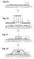
- FIGS. 1 a - 1 d show the process of manufacturing a wiring board according to the present invention and the condition of a completed power semiconductor module, wherein FIG. 1 a shows a metal base wiring board, FIG. 1 b shows the step of forming a built-up circuit pattern using a cold spray process, FIG. 1 c shows a condition in which a built-up circuit pattern has been formed, and FIG. 1 d shows a power semiconductor module in which a power semiconductor is mounted on a built-up circuit pattern;
- FIG. 2 is a diagram regarding a thickness of a built-up circuit pattern
- FIG. 3 is a view showing a cross-sectional structure of a conventional metal base wiring substrate
- FIGS. 4 a and 4 b show a cross-sectional structure of a conventional ceramics wiring board, wherein FIG. 4 a shows a ceramics wiring board, and FIG. 4 b shows a ceramics wiring board in which a base metal is bonded thereto; and
- FIG. 5 is a view showing a cross-sectional structure where a build-up circuit pattern is formed on an entire region of a circuit pattern.
- FIGS. 1 a - 1 d show the process of manufacturing a wiring board according to the present invention and the condition of a completed power semiconductor module, wherein FIG. 1 a shows a metal base wiring board, FIG. 1 b shows the step of forming a built-up circuit pattern using a cold spray process, FIG. 1 c shows a condition in which a built-up circuit pattern has been formed, and FIG. 1 d shows a power semiconductor module in which a power semiconductor is mounted on a built-up circuit pattern.
- a metal base wiring board is of a three-layer construction constituted by providing an insulating layer 2 containing inorganic filler on base metal 1 , and attaching a circuit pattern 3 on top of this.
- the circuit pattern 3 usually copper foil is employed. Aluminum foil could be employed for this circuit pattern 3 instead of copper foil.
- the copper foil that is attached to the insulating layer 2 is processed to the prescribed pattern by wet etching to produce the circuit pattern 3 .
- a standard product having a thickness of about 35 ⁇ m to 140 ⁇ m may normally be employed.
- the pattern thickness of the circuit pattern 3 is determined by the current capacity of the circuit, taking into consideration the costs of etching processing, the thickness of the copper foil should preferably be made as thin as possible.
- the metal base wiring board formed as described above is the same as the conventional metal base wiring board, but, in the case of a wiring board according to the present invention, the thickness is increased locally, exclusively in a region of the circuit pattern 3 where heat dissipation is desired to be improved.
- a mask 4 that is formed with a hole in the shape corresponding to the region where the thickness is desired to be increased is arranged on the circuit pattern 3 and metal powder is sprayed thereon from above at normal temperature and ultrasonic speed by the cold spray process, thereby laminating a layer of metal powder onto the circuit pattern 3 .
- a built-up circuit pattern 5 as shown in FIG. 1 c is formed.
- the cold spray process is considered to be a type of spray coating technique.
- Gas at a temperature lower than the melting point or softening temperature of the spray coating material is used to produce a gas current of ultrasonic speed; particles of spray coating material are accelerated by being injected into this current and a coating is formed by blasting the substrate with these particles still in the solid state.
- a characteristic feature of the cold spray process is that the temperature of the working gas that is used to heat/accelerate the spray coating material particles is much lower than in the case of, for example, the conventional plasma spray coating method, flame spray coating method or high-speed flame spray coating method.
- a high working gas temperature of 2000 to 8000° C.
- a working gas of ordinary temperature to about 600° C. may be employed.
- the spray coating material particles are made to collide with the substrate at high speed while still in the solid state without being heated to any great extent, when a critical speed is reached, plastic deformation of the substrate and the spray coating material particles takes place due to the energy of impact, resulting in the formation of a coating.
- oxidation or thermal denaturing of the spray coating material due to heat can be minimized.
- high-pressure gas supplied from a gas source such as a cylinder is branched to a powder supply device and a gas heater.
- the working gas constituting the main flow is raised in temperature by flowing through a gas pipe of coil shape that is directly or indirectly heated by, for example, an electric furnace, before being supplied to the spray coating gun where it is accelerated and sprayed by means of an ultrasonic speed nozzle.
- part of the working gas is branched to the powder supply device, where it acts as a carrier gas and is caused to flow into the rear of the spray coating gun together with the spray coating powder.
- heating of the working gas need not be performed, but such heating is advantageous in that heating makes it possible to use higher particle speeds and in order to facilitate generation of plastic deformation of the particles.
- Air, helium, or nitrogen may be employed as the gas.
- metal material of particle size 1 to 50 ⁇ m may be employed as the spray coating material that is sprayed onto the circuit pattern 3 .
- this particle material for example copper, aluminum, iron, titanium, molybdenum, or nickel may be employed.
- copper or aluminum is employed.
- These spray coating material particles are deposited by being blasted onto the circuit pattern 3 through the mask 4 separated by a distance of 10 to 50 mm, with a speed of 500 to 900 m/s: a built-up circuit pattern 5 is thereby formed on the circuit pattern 3 as shown in FIG. 1 c . Blasting with spray coating material particles is performed for a prescribed time in order to obtain the necessary film thickness of the built-up circuit pattern 5 .
- the thickness of the built-up circuit pattern 5 is set taking into account the loss generated by the power semiconductor. Although this depends on the amount of loss generated, the thickness of an effective built-up circuit pattern 5 is about 0.5 mm to 5 mm.
- a metal base wiring board of a three-layer structure wherein a built-up circuit pattern 5 is directly bonded with the copper foil is manufactured by the manufacturing steps described above. After this, a power semiconductor 6 is mounted on the built-up circuit pattern 5 that has been deposited by cold spraying. The power semiconductor 6 is usually bonded to the built-up circuit pattern 5 by means of SnPb-based solder or SnAgCu-based solder.
- wire 7 is normally used for the wire 7 .
- FIG. 2 is a diagram regarding the thickness of the built-up circuit pattern.
- the heat current that is generated from the power semiconductor 6 has the property of normally diffusing and spreading out at an angle of inclination of 45 degrees. If therefore the distance a from the chip edge of the power semiconductor 6 to the edge of the built-up circuit pattern 5 is equal to the thickness b of the sum of the circuit pattern 3 and built-up circuit pattern 5 , the heat spreading effect is manifested to a maximum, making it possible to greatly reduce the thermal resistance. There is therefore no need for useless increase in the width of the circuit pattern 3 and built-up circuit pattern 5 with respect to the size of the power semiconductor 6 and there is no need for useless increase in the thickness of the built-up circuit pattern 5 .
- the optimum ratio of the distance a from the edge of the mounted power semiconductor 6 to the edge of the built-up circuit pattern 5 and the thickness b of the sum of the circuit pattern 3 and built-up circuit pattern 5 is 1, a substantially satisfactory thermal diffusion effect can be obtained so long as this ratio is in the range of 0.8 to 1.2. If this ratio is less than 0.8, in some cases, sufficient thermal diffusion may not be obtained and if this ratio exceeds 1.2 the effect is saturated.
Abstract
Description
Claims (12)
Priority Applications (1)
| Application Number | Priority Date | Filing Date | Title |
|---|---|---|---|
| US12/585,913 US8336202B2 (en) | 2005-05-13 | 2009-09-29 | Method of manufacturing a wiring board |
Applications Claiming Priority (2)
| Application Number | Priority Date | Filing Date | Title |
|---|---|---|---|
| JP2005-140498 | 2005-05-13 | ||
| JP2005140498A JP4595665B2 (en) | 2005-05-13 | 2005-05-13 | Wiring board manufacturing method |
Related Child Applications (1)
| Application Number | Title | Priority Date | Filing Date |
|---|---|---|---|
| US12/585,913 Division US8336202B2 (en) | 2005-05-13 | 2009-09-29 | Method of manufacturing a wiring board |
Publications (2)
| Publication Number | Publication Date |
|---|---|
| US20060258055A1 US20060258055A1 (en) | 2006-11-16 |
| US7626124B2 true US7626124B2 (en) | 2009-12-01 |
Family
ID=37311270
Family Applications (2)
| Application Number | Title | Priority Date | Filing Date |
|---|---|---|---|
| US11/358,143 Active US7626124B2 (en) | 2005-05-13 | 2006-02-22 | Wiring board |
| US12/585,913 Active 2027-09-02 US8336202B2 (en) | 2005-05-13 | 2009-09-29 | Method of manufacturing a wiring board |
Family Applications After (1)
| Application Number | Title | Priority Date | Filing Date |
|---|---|---|---|
| US12/585,913 Active 2027-09-02 US8336202B2 (en) | 2005-05-13 | 2009-09-29 | Method of manufacturing a wiring board |
Country Status (4)
| Country | Link |
|---|---|
| US (2) | US7626124B2 (en) |
| JP (1) | JP4595665B2 (en) |
| CN (1) | CN100570866C (en) |
| DE (1) | DE102006019602B4 (en) |
Cited By (5)
| Publication number | Priority date | Publication date | Assignee | Title |
|---|---|---|---|---|
| US20080066955A1 (en) * | 2006-09-15 | 2008-03-20 | Takamasa Nodo | Surface mounting structure for a surface mounting electronic component |
| US11562967B2 (en) * | 2020-04-06 | 2023-01-24 | Infineon Technologies Ag | Method for fabricating a semiconductor package, semiconductor package and embedded PCB module |
| US11662300B2 (en) | 2019-09-19 | 2023-05-30 | Westinghouse Electric Company Llc | Apparatus for performing in-situ adhesion test of cold spray deposits and method of employing |
| US11898986B2 (en) | 2012-10-10 | 2024-02-13 | Westinghouse Electric Company Llc | Systems and methods for steam generator tube analysis for detection of tube degradation |
| US11935662B2 (en) | 2019-07-02 | 2024-03-19 | Westinghouse Electric Company Llc | Elongate SiC fuel elements |
Families Citing this family (50)
| Publication number | Priority date | Publication date | Assignee | Title |
|---|---|---|---|---|
| JP4662361B2 (en) * | 2006-01-23 | 2011-03-30 | 株式会社小糸製作所 | Light source module |
| JP2008053548A (en) * | 2006-08-25 | 2008-03-06 | Sharp Corp | Circuit board and inspection method thereof |
| US7957158B2 (en) * | 2006-10-31 | 2011-06-07 | Sanyo Electric Co., Ltd. | Circuit device |
| DE102006061435A1 (en) * | 2006-12-23 | 2008-06-26 | Leoni Ag | Method and device for spraying in particular a conductor track, electrical component with a conductor track and metering device |
| KR100834515B1 (en) * | 2007-03-07 | 2008-06-02 | 삼성전기주식회사 | Method for forming photoresist-laminated substrate, method for plating insulating substrate, method for surface treating metal layer of circuit board, and method for manufacturing multi layer ceramic condenser using metal nanoparticles aerosol |
| JP4986657B2 (en) * | 2007-03-09 | 2012-07-25 | パナソニック株式会社 | Brushless motor |
| JP5144657B2 (en) * | 2007-05-30 | 2013-02-13 | 京セラ株式会社 | Laminated heat dissipation base, heat dissipation unit using the same, and electronic device |
| DE102007050405B4 (en) * | 2007-10-22 | 2010-09-09 | Continental Automotive Gmbh | Electrical power component, in particular power semiconductor module, with a cooling device and method for surface and heat-conducting bonding of a cooling device to an electrical power component |
| US20090141456A1 (en) * | 2007-11-30 | 2009-06-04 | Itt Manufacturing Enterprises, Inc. | Multilayer, thermally-stabilized substrate structures |
| JP5321942B2 (en) * | 2008-02-29 | 2013-10-23 | 新東工業株式会社 | Method for manufacturing electronic circuit board and electronic circuit board |
| KR101013078B1 (en) * | 2008-05-09 | 2011-02-08 | (주)세렉트론 | Method of fabrication electrode using cold spray and electrode by the same |
| DE102009033029A1 (en) | 2009-07-02 | 2011-01-05 | Electrovac Ag | Electronic device |
| JP5359644B2 (en) * | 2009-07-23 | 2013-12-04 | 三菱マテリアル株式会社 | Power module substrate, power module, and method of manufacturing power module substrate |
| EP2315242A1 (en) * | 2009-10-23 | 2011-04-27 | ABB Technology AG | Circuit arrangement and manufacturing method thereof |
| JP5186528B2 (en) * | 2010-04-23 | 2013-04-17 | 日本発條株式会社 | Conductive member and manufacturing method thereof |
| EP2571050A4 (en) | 2010-05-12 | 2017-10-04 | Toyota Jidosha Kabushiki Kaisha | Semiconductor device |
| EP2573809A4 (en) | 2010-05-18 | 2017-05-24 | Toyota Jidosha Kabushiki Kaisha | Semiconductor device and method for manufacturing the same |
| WO2011145202A1 (en) * | 2010-05-21 | 2011-11-24 | トヨタ自動車株式会社 | Semiconductor device |
| DE102010039728A1 (en) * | 2010-08-25 | 2012-03-01 | Robert Bosch Gmbh | Method for producing an electrical circuit and electrical circuit |
| US20120193126A1 (en) * | 2011-01-31 | 2012-08-02 | General Electric Company | Method of forming sensors and circuits on components |
| JP2013012531A (en) * | 2011-06-28 | 2013-01-17 | Kyocera Corp | Member for mounting electronic component and electronic apparatus |
| JP6125527B2 (en) * | 2012-11-06 | 2017-05-10 | 日本碍子株式会社 | Light emitting diode substrate and method for manufacturing light emitting diode substrate |
| EP2919287B1 (en) * | 2012-11-06 | 2019-12-25 | NGK Insulators, Ltd. | Substrate for light emitting diodes |
| DE102012224376A1 (en) * | 2012-12-27 | 2014-07-03 | Robert Bosch Gmbh | Printed circuit arrangement and method for its production |
| JP6037885B2 (en) * | 2013-02-19 | 2016-12-07 | 三菱重工業株式会社 | Deposition method |
| US9147631B2 (en) | 2013-04-17 | 2015-09-29 | Infineon Technologies Austria Ag | Semiconductor power device having a heat sink |
| EP3093882B1 (en) * | 2014-01-10 | 2021-02-17 | Furukawa Electric Co. Ltd. | Electronic circuit device |
| CN103841784A (en) * | 2014-03-18 | 2014-06-04 | 亚超特工业有限公司 | Forming method of internal middle frame board of electronic device and internal middle frame board |
| DE102014217186A1 (en) * | 2014-08-28 | 2016-03-03 | Continental Automotive Gmbh | Method for producing a circuit carrier and circuit carrier for electronic components |
| CN104363697B (en) * | 2014-10-16 | 2017-12-29 | 金壬海 | The aluminium substrate copper-clad plate of ceramic filler medium and its manufacture method |
| DE102015201927A1 (en) * | 2015-02-04 | 2016-08-04 | Siemens Aktiengesellschaft | Method for cold gas spraying with mask |
| JP6400501B2 (en) * | 2015-02-18 | 2018-10-03 | Dowaメタルテック株式会社 | Metal-ceramic circuit board manufacturing method |
| JP6370257B2 (en) * | 2015-04-27 | 2018-08-08 | 三菱電機株式会社 | Semiconductor device |
| KR102424402B1 (en) | 2015-08-13 | 2022-07-25 | 삼성전자주식회사 | Semiconductor packages and methods for fabricating the same |
| JP6454262B2 (en) * | 2015-12-24 | 2019-01-16 | タツタ電線株式会社 | Solder connection structure and film forming method |
| DE102016001810A1 (en) * | 2016-02-17 | 2017-08-17 | Häusermann GmbH | Method for producing a printed circuit board with reinforced copper structure |
| US9532448B1 (en) * | 2016-03-03 | 2016-12-27 | Ford Global Technologies, Llc | Power electronics modules |
| CN106158764A (en) * | 2016-08-30 | 2016-11-23 | 无锡新洁能股份有限公司 | Power model base plate and power model |
| US11160172B2 (en) * | 2017-01-17 | 2021-10-26 | Denka Company Limited | Method for producing ceramic circuit board |
| CN110476244B (en) | 2017-03-31 | 2023-11-03 | 罗姆股份有限公司 | Power module and method for manufacturing the same |
| JP7369508B2 (en) * | 2017-08-04 | 2023-10-26 | デンカ株式会社 | ceramic circuit board |
| JP7299671B2 (en) * | 2017-08-04 | 2023-06-28 | デンカ株式会社 | ceramic circuit board |
| WO2019036304A1 (en) * | 2017-08-18 | 2019-02-21 | Thin Film Electronics Asa | Spray coated sense lines, security and/or identification tags and devices including the same, and methods of manufacturing |
| JP6847259B2 (en) * | 2017-11-22 | 2021-03-24 | 三菱電機株式会社 | Semiconductor devices and methods for manufacturing semiconductor devices |
| DE102019215793A1 (en) * | 2019-10-14 | 2021-04-15 | Vitesco Technologies GmbH | Wiring substrate for a semiconductor device and method for manufacturing a wiring substrate |
| DE102020202607A1 (en) * | 2020-02-28 | 2021-09-02 | Siemens Aktiengesellschaft | Electronic module, method for manufacturing an electronic module and industrial plant |
| KR20210117587A (en) | 2020-03-19 | 2021-09-29 | 삼성전자주식회사 | Semiconductor module |
| CN111867259A (en) * | 2020-07-30 | 2020-10-30 | 南京凯泰化学科技有限公司 | Preparation method of ceramic copper-clad plate |
| JP7428261B2 (en) * | 2020-08-28 | 2024-02-06 | 富士電機株式会社 | semiconductor equipment |
| JP2022094661A (en) * | 2020-12-15 | 2022-06-27 | 三菱マテリアル株式会社 | Insulated circuit board and manufacturing method for the same |
Citations (24)
| Publication number | Priority date | Publication date | Assignee | Title |
|---|---|---|---|---|
| US4521476A (en) * | 1982-08-19 | 1985-06-04 | Denki Kagaku Kogyo Kabushiki Kaisha | Hybrid integrated circuit and preparation thereof |
| US4811166A (en) * | 1986-07-02 | 1989-03-07 | Texas Instruments Incorporated | Heat dissipating member for mounting a semiconductor device and electrical circuit unit incorporating the member |
| US5348683A (en) | 1990-02-06 | 1994-09-20 | Olin Corporation | Chloric acid - alkali metal chlorate mixtures and chlorine dioxide generation |
| US5362926A (en) * | 1991-07-24 | 1994-11-08 | Denki Kagaku Kogyo Kabushiki Kaisha | Circuit substrate for mounting a semiconductor element |
| US5384683A (en) * | 1991-11-07 | 1995-01-24 | Kabushiki Kaisha Toshiba | Intelligent power device module |
| US5393568A (en) * | 1992-02-28 | 1995-02-28 | Thomas J. Valente | Metalized coating process |
| JPH07122696A (en) | 1993-10-27 | 1995-05-12 | Nippon Steel Corp | Semiconductor device |
| US5469131A (en) * | 1992-08-28 | 1995-11-21 | Sanyo Electric Co., Ltd. | Hybrid integrated circuit device |
| DE19963264A1 (en) | 1999-12-17 | 2001-06-21 | Sli Miniature Lighting Gmbh | Support material for electronic high heat-dissipation component in surface mounted device technology; has metal core, insulation layer with top and bottom connection structures and metal coating |
| JP2002012653A (en) | 2000-07-03 | 2002-01-15 | Denki Kagaku Kogyo Kk | Curable resin composition and metal-base circuit board using the same |
| JP2002076549A (en) | 2000-08-24 | 2002-03-15 | Denki Kagaku Kogyo Kk | Metal base circuit board |
| JP2002114836A (en) | 2000-10-10 | 2002-04-16 | Denki Kagaku Kogyo Kk | Curable resin composition and metal base circuit board using the same |
| US6570099B1 (en) * | 1999-11-09 | 2003-05-27 | Matsushita Electric Industrial Co., Ltd. | Thermal conductive substrate and the method for manufacturing the same |
| JP2003229508A (en) | 2001-11-28 | 2003-08-15 | Nitto Shinko Kk | High heat dissipation insulating substrate and module using it |
| US6627814B1 (en) * | 2002-03-22 | 2003-09-30 | David H. Stark | Hermetically sealed micro-device package with window |
| US20040079957A1 (en) | 2002-09-04 | 2004-04-29 | Andrews Peter Scott | Power surface mount light emitting die package |
| US6737153B2 (en) * | 2000-07-18 | 2004-05-18 | Matsushita Electric Industrial Co., Ltd. | Circuit board and method for manufacturing the same, and electronic apparatus comprising it |
| US6740903B2 (en) | 2002-04-15 | 2004-05-25 | Citizen Electronics Co., Ltd. | Substrate for light emitting diodes |
| JP2005005638A (en) | 2003-04-15 | 2005-01-06 | Fuji Electric Fa Components & Systems Co Ltd | Semiconductor module and its manufacturing method |
| US20050147742A1 (en) * | 2004-01-07 | 2005-07-07 | Tokyo Electron Limited | Processing chamber components, particularly chamber shields, and method of controlling temperature thereof |
| US20060093736A1 (en) * | 2004-10-29 | 2006-05-04 | Derek Raybould | Aluminum articles with wear-resistant coatings and methods for applying the coatings onto the articles |
| US7128948B2 (en) * | 2003-10-20 | 2006-10-31 | The Boeing Company | Sprayed preforms for forming structural members |
| US7232957B2 (en) * | 2003-09-25 | 2007-06-19 | Sanyo Electric Co., Ltd. | Hybrid integrated circuit device and method of manufacturing the same |
| US7476422B2 (en) | 2002-05-23 | 2009-01-13 | Delphi Technologies, Inc. | Copper circuit formed by kinetic spray |
Family Cites Families (6)
| Publication number | Priority date | Publication date | Assignee | Title |
|---|---|---|---|---|
| JPS6351690A (en) | 1986-08-20 | 1988-03-04 | 松下電工株式会社 | Manufacture of ceramic wiring board |
| JPH0831546B2 (en) | 1987-07-22 | 1996-03-27 | 電気化学工業株式会社 | High power circuit board and hybrid integrated circuit thereof |
| JPH0778901A (en) | 1993-06-18 | 1995-03-20 | Sumitomo Electric Ind Ltd | Semiconductor device |
| JP2002203942A (en) * | 2000-12-28 | 2002-07-19 | Fuji Electric Co Ltd | Power semiconductor module |
| US6808817B2 (en) * | 2002-03-15 | 2004-10-26 | Delphi Technologies, Inc. | Kinetically sprayed aluminum metal matrix composites for thermal management |
| DE10331208A1 (en) * | 2003-07-10 | 2005-02-10 | Newspray Gmbh | Method for securing electric or electronic components, generating waste heat, to cooler of aluminum, or its alloy, with cooler enameled, at least in fastening region of components, |
-
2005
- 2005-05-13 JP JP2005140498A patent/JP4595665B2/en active Active
-
2006
- 2006-02-22 US US11/358,143 patent/US7626124B2/en active Active
- 2006-02-28 CN CNB2006100515605A patent/CN100570866C/en active Active
- 2006-04-27 DE DE102006019602.3A patent/DE102006019602B4/en active Active
-
2009
- 2009-09-29 US US12/585,913 patent/US8336202B2/en active Active
Patent Citations (24)
| Publication number | Priority date | Publication date | Assignee | Title |
|---|---|---|---|---|
| US4521476A (en) * | 1982-08-19 | 1985-06-04 | Denki Kagaku Kogyo Kabushiki Kaisha | Hybrid integrated circuit and preparation thereof |
| US4811166A (en) * | 1986-07-02 | 1989-03-07 | Texas Instruments Incorporated | Heat dissipating member for mounting a semiconductor device and electrical circuit unit incorporating the member |
| US5348683A (en) | 1990-02-06 | 1994-09-20 | Olin Corporation | Chloric acid - alkali metal chlorate mixtures and chlorine dioxide generation |
| US5362926A (en) * | 1991-07-24 | 1994-11-08 | Denki Kagaku Kogyo Kabushiki Kaisha | Circuit substrate for mounting a semiconductor element |
| US5384683A (en) * | 1991-11-07 | 1995-01-24 | Kabushiki Kaisha Toshiba | Intelligent power device module |
| US5393568A (en) * | 1992-02-28 | 1995-02-28 | Thomas J. Valente | Metalized coating process |
| US5469131A (en) * | 1992-08-28 | 1995-11-21 | Sanyo Electric Co., Ltd. | Hybrid integrated circuit device |
| JPH07122696A (en) | 1993-10-27 | 1995-05-12 | Nippon Steel Corp | Semiconductor device |
| US6570099B1 (en) * | 1999-11-09 | 2003-05-27 | Matsushita Electric Industrial Co., Ltd. | Thermal conductive substrate and the method for manufacturing the same |
| DE19963264A1 (en) | 1999-12-17 | 2001-06-21 | Sli Miniature Lighting Gmbh | Support material for electronic high heat-dissipation component in surface mounted device technology; has metal core, insulation layer with top and bottom connection structures and metal coating |
| JP2002012653A (en) | 2000-07-03 | 2002-01-15 | Denki Kagaku Kogyo Kk | Curable resin composition and metal-base circuit board using the same |
| US6737153B2 (en) * | 2000-07-18 | 2004-05-18 | Matsushita Electric Industrial Co., Ltd. | Circuit board and method for manufacturing the same, and electronic apparatus comprising it |
| JP2002076549A (en) | 2000-08-24 | 2002-03-15 | Denki Kagaku Kogyo Kk | Metal base circuit board |
| JP2002114836A (en) | 2000-10-10 | 2002-04-16 | Denki Kagaku Kogyo Kk | Curable resin composition and metal base circuit board using the same |
| JP2003229508A (en) | 2001-11-28 | 2003-08-15 | Nitto Shinko Kk | High heat dissipation insulating substrate and module using it |
| US6627814B1 (en) * | 2002-03-22 | 2003-09-30 | David H. Stark | Hermetically sealed micro-device package with window |
| US6740903B2 (en) | 2002-04-15 | 2004-05-25 | Citizen Electronics Co., Ltd. | Substrate for light emitting diodes |
| US7476422B2 (en) | 2002-05-23 | 2009-01-13 | Delphi Technologies, Inc. | Copper circuit formed by kinetic spray |
| US20040079957A1 (en) | 2002-09-04 | 2004-04-29 | Andrews Peter Scott | Power surface mount light emitting die package |
| JP2005005638A (en) | 2003-04-15 | 2005-01-06 | Fuji Electric Fa Components & Systems Co Ltd | Semiconductor module and its manufacturing method |
| US7232957B2 (en) * | 2003-09-25 | 2007-06-19 | Sanyo Electric Co., Ltd. | Hybrid integrated circuit device and method of manufacturing the same |
| US7128948B2 (en) * | 2003-10-20 | 2006-10-31 | The Boeing Company | Sprayed preforms for forming structural members |
| US20050147742A1 (en) * | 2004-01-07 | 2005-07-07 | Tokyo Electron Limited | Processing chamber components, particularly chamber shields, and method of controlling temperature thereof |
| US20060093736A1 (en) * | 2004-10-29 | 2006-05-04 | Derek Raybould | Aluminum articles with wear-resistant coatings and methods for applying the coatings onto the articles |
Cited By (6)
| Publication number | Priority date | Publication date | Assignee | Title |
|---|---|---|---|---|
| US20080066955A1 (en) * | 2006-09-15 | 2008-03-20 | Takamasa Nodo | Surface mounting structure for a surface mounting electronic component |
| US8263875B2 (en) * | 2006-09-15 | 2012-09-11 | Kabushiki Kaisha Toyota Jidoshokki | Surface mounting structure for a surface mounting electronic component |
| US11898986B2 (en) | 2012-10-10 | 2024-02-13 | Westinghouse Electric Company Llc | Systems and methods for steam generator tube analysis for detection of tube degradation |
| US11935662B2 (en) | 2019-07-02 | 2024-03-19 | Westinghouse Electric Company Llc | Elongate SiC fuel elements |
| US11662300B2 (en) | 2019-09-19 | 2023-05-30 | Westinghouse Electric Company Llc | Apparatus for performing in-situ adhesion test of cold spray deposits and method of employing |
| US11562967B2 (en) * | 2020-04-06 | 2023-01-24 | Infineon Technologies Ag | Method for fabricating a semiconductor package, semiconductor package and embedded PCB module |
Also Published As
| Publication number | Publication date |
|---|---|
| US20100041228A1 (en) | 2010-02-18 |
| DE102006019602A1 (en) | 2006-11-23 |
| US8336202B2 (en) | 2012-12-25 |
| US20060258055A1 (en) | 2006-11-16 |
| CN100570866C (en) | 2009-12-16 |
| DE102006019602B4 (en) | 2021-01-28 |
| CN1862795A (en) | 2006-11-15 |
| JP2006319146A (en) | 2006-11-24 |
| JP4595665B2 (en) | 2010-12-08 |
Similar Documents
| Publication | Publication Date | Title |
|---|---|---|
| US7626124B2 (en) | Wiring board | |
| JP5077529B2 (en) | Insulating substrate manufacturing method and semiconductor device manufacturing method | |
| US9373555B2 (en) | Power semiconductor module, method for manufacturing the same, and power converter | |
| US7256431B2 (en) | Insulating substrate and semiconductor device having a thermally sprayed circuit pattern | |
| JP6024750B2 (en) | Semiconductor module | |
| KR101585142B1 (en) | Heat dissipation structure, power module, method for manufacturing heat dissipation structure and method for manufacturing power module | |
| JP6332439B2 (en) | Power converter | |
| JP4023397B2 (en) | Semiconductor module and manufacturing method thereof | |
| JP5971333B2 (en) | Power converter | |
| WO2015064430A1 (en) | Laminate body, insulating cooling plate, power module, and production method for laminate body | |
| KR20110109931A (en) | Cooling device | |
| US9318352B2 (en) | Power module package and method for manufacturing the same | |
| JP2006278558A (en) | Insulated heat transmission structure and substrate for use of power module | |
| WO2016021561A1 (en) | Composite substrate and power module | |
| WO2013065316A1 (en) | Power converter | |
| CN103378050A (en) | Electronic assemblies and methods of fabricating electronic assemblies | |
| JP5644806B2 (en) | Insulating substrate, semiconductor device and manufacturing method thereof | |
| JP2013168421A (en) | Wiring board and manufacturing method of the same | |
| JP2010511297A (en) | Electronic member module and manufacturing method thereof | |
| JP5875102B2 (en) | Manufacturing method of semiconductor module | |
| US20230254970A1 (en) | Circuit board | |
| JP2010239164A (en) | Wiring board | |
| US11081421B2 (en) | IGBT module with heat dissipation structure having ceramic layers corresponding in position and in area to chips | |
| US20230247762A1 (en) | Circuit board |
Legal Events
| Date | Code | Title | Description |
|---|---|---|---|
| AS | Assignment |
Owner name: FUJI ELECTRIC HOLDINGS CO., LTD., JAPAN Free format text: ASSIGNMENT OF ASSIGNORS INTEREST;ASSIGNOR:OKAMOTO, KENJI;REEL/FRAME:017721/0500 Effective date: 20060320 |
|
| STCF | Information on status: patent grant |
Free format text: PATENTED CASE |
|
| FEPP | Fee payment procedure |
Free format text: PAYOR NUMBER ASSIGNED (ORIGINAL EVENT CODE: ASPN); ENTITY STATUS OF PATENT OWNER: LARGE ENTITY |
|
| AS | Assignment |
Owner name: FUJI ELECTRIC SYSTEMS CO., LTD.,JAPAN Free format text: ASSIGNMENT OF ASSIGNORS INTEREST;ASSIGNOR:FUJI ELECTRIC DEVICE TECHNOLOGY CO., LTD.;REEL/FRAME:024252/0451 Effective date: 20090930 Owner name: FUJI ELECTRIC SYSTEMS CO., LTD., JAPAN Free format text: ASSIGNMENT OF ASSIGNORS INTEREST;ASSIGNOR:FUJI ELECTRIC DEVICE TECHNOLOGY CO., LTD.;REEL/FRAME:024252/0451 Effective date: 20090930 |
|
| AS | Assignment |
Owner name: FUJI ELECTRIC CO., LTD., JAPAN Free format text: MERGER AND CHANGE OF NAME;ASSIGNORS:FUJI ELECTRIC SYSTEMS CO., LTD. (FES);FUJI TECHNOSURVEY CO., LTD. (MERGER BY ABSORPTION);REEL/FRAME:026970/0872 Effective date: 20110401 |
|
| FPAY | Fee payment |
Year of fee payment: 4 |
|
| FPAY | Fee payment |
Year of fee payment: 8 |
|
| MAFP | Maintenance fee payment |
Free format text: PAYMENT OF MAINTENANCE FEE, 12TH YEAR, LARGE ENTITY (ORIGINAL EVENT CODE: M1553); ENTITY STATUS OF PATENT OWNER: LARGE ENTITY Year of fee payment: 12 |