US7670950B2 - Copper metallization of through silicon via - Google Patents
Copper metallization of through silicon via Download PDFInfo
- Publication number
- US7670950B2 US7670950B2 US12/185,641 US18564108A US7670950B2 US 7670950 B2 US7670950 B2 US 7670950B2 US 18564108 A US18564108 A US 18564108A US 7670950 B2 US7670950 B2 US 7670950B2
- Authority
- US
- United States
- Prior art keywords
- copper
- microns
- via feature
- feature
- concentration
- Prior art date
- Legal status (The legal status is an assumption and is not a legal conclusion. Google has not performed a legal analysis and makes no representation as to the accuracy of the status listed.)
- Active
Links
- 0 C.[2*]C[1*]S(=O)(=O)[O-] Chemical compound C.[2*]C[1*]S(=O)(=O)[O-] 0.000 description 3
- BXOFJAYGXCDBFG-UHFFFAOYSA-L C.C.O=S(=O)([O-])CCCSSCCCS(=O)(=O)[O-] Chemical compound C.C.O=S(=O)([O-])CCCSSCCCS(=O)(=O)[O-] BXOFJAYGXCDBFG-UHFFFAOYSA-L 0.000 description 1
- CBYLJEMZLSCTLI-UHFFFAOYSA-L C.O=S(=O)([O-])CCCSSCCCS(=O)(=O)[O-].[Na+] Chemical compound C.O=S(=O)([O-])CCCSSCCCS(=O)(=O)[O-].[Na+] CBYLJEMZLSCTLI-UHFFFAOYSA-L 0.000 description 1
- HWGKFJWMWCWSGV-UHFFFAOYSA-M C=CC1=CC=NC=C1.C=CC1=CC=[N+](C)C=C1.CCC(CC)C1=CC=N(C)C=C1.CO.COS(=O)(=O)O.COS(=O)(=O)OC.COS(=O)(=O)[O-] Chemical compound C=CC1=CC=NC=C1.C=CC1=CC=[N+](C)C=C1.CCC(CC)C1=CC=N(C)C=C1.CO.COS(=O)(=O)O.COS(=O)(=O)OC.COS(=O)(=O)[O-] HWGKFJWMWCWSGV-UHFFFAOYSA-M 0.000 description 1
- DCTPILKGUYHKGK-UHFFFAOYSA-N O=S(=O)(O)CCCCO.O=S(=O)(O)CCCSSSSCCCS(=O)(=O)O.O=S(CCCS(=O)(=O)O)S(=O)SCCCS(=O)(=O)O.O=S(CCCS(=O)(=O)O)SSSCCCS(=O)(=O)O.O=S(SCCCS(=O)(=O)O)SSCCCS(=O)(=O)O Chemical compound O=S(=O)(O)CCCCO.O=S(=O)(O)CCCSSSSCCCS(=O)(=O)O.O=S(CCCS(=O)(=O)O)S(=O)SCCCS(=O)(=O)O.O=S(CCCS(=O)(=O)O)SSSCCCS(=O)(=O)O.O=S(SCCCS(=O)(=O)O)SSCCCS(=O)(=O)O DCTPILKGUYHKGK-UHFFFAOYSA-N 0.000 description 1
- LMPMFQXUJXPWSL-UHFFFAOYSA-N O=S(=O)(O)CCCSSCCCS(=O)(=O)O Chemical compound O=S(=O)(O)CCCSSCCCS(=O)(=O)O LMPMFQXUJXPWSL-UHFFFAOYSA-N 0.000 description 1
Images


Classifications
-
- H—ELECTRICITY
- H01—ELECTRIC ELEMENTS
- H01L—SEMICONDUCTOR DEVICES NOT COVERED BY CLASS H10
- H01L21/00—Processes or apparatus adapted for the manufacture or treatment of semiconductor or solid state devices or of parts thereof
- H01L21/70—Manufacture or treatment of devices consisting of a plurality of solid state components formed in or on a common substrate or of parts thereof; Manufacture of integrated circuit devices or of parts thereof
- H01L21/71—Manufacture of specific parts of devices defined in group H01L21/70
- H01L21/768—Applying interconnections to be used for carrying current between separate components within a device comprising conductors and dielectrics
- H01L21/76898—Applying interconnections to be used for carrying current between separate components within a device comprising conductors and dielectrics formed through a semiconductor substrate
-
- C—CHEMISTRY; METALLURGY
- C25—ELECTROLYTIC OR ELECTROPHORETIC PROCESSES; APPARATUS THEREFOR
- C25D—PROCESSES FOR THE ELECTROLYTIC OR ELECTROPHORETIC PRODUCTION OF COATINGS; ELECTROFORMING; APPARATUS THEREFOR
- C25D3/00—Electroplating: Baths therefor
- C25D3/02—Electroplating: Baths therefor from solutions
- C25D3/38—Electroplating: Baths therefor from solutions of copper
-
- C—CHEMISTRY; METALLURGY
- C25—ELECTROLYTIC OR ELECTROPHORETIC PROCESSES; APPARATUS THEREFOR
- C25D—PROCESSES FOR THE ELECTROLYTIC OR ELECTROPHORETIC PRODUCTION OF COATINGS; ELECTROFORMING; APPARATUS THEREFOR
- C25D5/00—Electroplating characterised by the process; Pretreatment or after-treatment of workpieces
- C25D5/02—Electroplating of selected surface areas
-
- C—CHEMISTRY; METALLURGY
- C25—ELECTROLYTIC OR ELECTROPHORETIC PROCESSES; APPARATUS THEREFOR
- C25D—PROCESSES FOR THE ELECTROLYTIC OR ELECTROPHORETIC PRODUCTION OF COATINGS; ELECTROFORMING; APPARATUS THEREFOR
- C25D7/00—Electroplating characterised by the article coated
- C25D7/12—Semiconductors
- C25D7/123—Semiconductors first coated with a seed layer or a conductive layer
-
- H—ELECTRICITY
- H01—ELECTRIC ELEMENTS
- H01L—SEMICONDUCTOR DEVICES NOT COVERED BY CLASS H10
- H01L21/00—Processes or apparatus adapted for the manufacture or treatment of semiconductor or solid state devices or of parts thereof
- H01L21/02—Manufacture or treatment of semiconductor devices or of parts thereof
- H01L21/04—Manufacture or treatment of semiconductor devices or of parts thereof the devices having at least one potential-jump barrier or surface barrier, e.g. PN junction, depletion layer or carrier concentration layer
- H01L21/18—Manufacture or treatment of semiconductor devices or of parts thereof the devices having at least one potential-jump barrier or surface barrier, e.g. PN junction, depletion layer or carrier concentration layer the devices having semiconductor bodies comprising elements of Group IV of the Periodic System or AIIIBV compounds with or without impurities, e.g. doping materials
- H01L21/28—Manufacture of electrodes on semiconductor bodies using processes or apparatus not provided for in groups H01L21/20 - H01L21/268
- H01L21/283—Deposition of conductive or insulating materials for electrodes conducting electric current
- H01L21/288—Deposition of conductive or insulating materials for electrodes conducting electric current from a liquid, e.g. electrolytic deposition
- H01L21/2885—Deposition of conductive or insulating materials for electrodes conducting electric current from a liquid, e.g. electrolytic deposition using an external electrical current, i.e. electro-deposition
Definitions
- the present invention generally relates to a method and composition for filling through silicon via with copper metallization.
- An interconnect feature is a feature such as a via or trench formed in a dielectric substrate which is then filled with metal, typically copper, to yield an electrically conductive interconnect. Copper, having better conductivity than any metal except silver, is the metal of choice since copper metallization allows for smaller features and uses less energy to pass electricity.
- damascene processing interconnect features of semiconductor IC devices are metallized using electrolytic copper deposition.
- substrates include patterned silicon wafers and dielectric films such as, for example, SiO2 or low- ⁇ dielectrics.
- Low- ⁇ dielectric materials are desirable since such materials exhibit reduced parasitic capacitance compared to the same thickness of SiO2 dielectric, enabling increased feature density, faster switching speeds, and lower heat dissipation.
- Low- ⁇ dielectric materials can be categorized by type (silicates, fluorosilicates and organo-silicates, organic polymeric etc.) and by deposition technique (CVD; spin-on). Dielectric constant reduction may be achieved by reducing polarizability, by reducing density, or by introducing porosity.
- a patterned semiconductor integrated circuit device substrate may comprise both small and large interconnect features.
- a wafer has layers of integrated circuitry, e.g., processors, programmable devices, memory devices, and the like, built in a silicon substrate.
- integrated circuit (IC) devices have been manufactured to contain small diameter vias and sub-micron sized trenches that form electrical connections between layers of interconnect structure. These features have dimensions on the order of about 150 nanometers or less, such as about 90 nanometers, 65 nanometers, or even 45 nanometers.
- Copper damascene metallization relies on superfilling additives, i.e., a combination of additives that are referred to in the art as accelerators, levelers, and suppressors. These additives act in conjunction in a manner that can flawlessly fill copper into the interconnect features (often called “superfilling” or “bottom up” growth). See, for example, Too et al., U.S. Pat. No. 6,776,893 and Commander et al., U.S. Pub. No. 2003/0168343, the disclosures of which are hereby incorporated as if set forth in their entireties.
- superfilling additives i.e., a combination of additives that are referred to in the art as accelerators, levelers, and suppressors. These additives act in conjunction in a manner that can flawlessly fill copper into the interconnect features (often called “superfilling” or “bottom up” growth). See, for example, Too et al., U.S. Pat. No. 6,776,893 and
- a wafer may be constructed to comprise one or more large diameter vias.
- This type of via architecture is known in the art as a “through silicon via” (TSV).
- TSV through silicon via
- through silicon via allows electrical interconnection between 2 or more wafers bonded to each other in a three-dimensional wafer stack.
- the 3D wafer stack may be diced into stacked dies (“chips”), each stacked chip having multiple tiers (“layers”) of integrated circuitry.
- chips stacked dies
- layers multiple tiers
- the vias can be characterized as “Via First—Before FEOL”, or “Via First—After BEOL”.
- the vias are made before wafer/die attachment or bonding.
- the third category of TSV is via last, which means the via is constructed after wafer/die attachment or bonding.
- Through silicon vias are critical components of three-dimensional integrated circuits, and they can be found in RF devices, MEMs, CMOS image sensors, Flash, DRAM, SRAM memories, analog devices, and logic devices.
- the depth of a TSV depends on the via type (via first or via last), and the application. Via depth varies from 20 microns to 500 microns, typically between about 50 microns and about 250 microns. Via openings in TSV have an entry dimension such as a diameter on the order of between about 200 nm to about 200 microns, typically between about 25 microns and about 75 microns.
- the typical aspect ratio for a through silicon via is from 0.3:1 to greater than 20:1.
- compositions appropriate for damascene metallization i.e., the composition comprises the three component superfilling additives including accelerator, suppressor, and leveler
- the composition comprises the three component superfilling additives including accelerator, suppressor, and leveler
- plating durations as long as 20 hours to completely metallize large dimension (e.g., greater than 50 micron diameter openings) through silicon via.
- Arana et al. (U.S. 2007/0001266, Intel Corporation) disclose a method for filling through silicon via by incorporating particles into the copper metallization, the particles having a different coefficient of thermal expansion than the copper matrix.
- the stated purpose is to reduce stress variations between the copper metallization matrix and the silicon possibly caused by the differing bulk CTE of the respective materials.
- the reference does not include actual electrolytic copper plating chemistry, nor does the reference state that their electrolytic plating method incorporating particles in the deposition composition reduces through silicon via fill time.
- Lane et al. (U.S. Pat. No. 7,081,408, Intel Corporation) disclose a method for filling through silicon via features. Although they discuss filling the through silicon via with copper metallization by any suitable process, for example, electrolytic deposition, Lane et al. do not disclose actual electrolytic copper plating chemistry, nor do they disclose the duration necessary to achieve copper filling.
- Copper plating is also known from, e.g., also Eilert (U.S. Pat. No. 7,111,149); Rumer et al. (U.S. Pat. No. 6,924,551); Shi et al. (U.S. Pub. No. 2007/0085198); Ramanathan et al. (U.S. Pub. No. 2007/0117348) Heck et al. (U.S. Pub. No. 2006/0264029); Williams et al. (U.S. Pub. No. 2006/0273455); Rangel (U.S. Pub. No. 2006/0278979); and Savastiouk et al. (U.S. Pub. No. 2005/0136635); but none of these references, which relate to through silicon via architectures and methods, disclose applicable copper metallization chemistries or plating durations sufficient to fill through silicon via features.
- the present invention is directed to a method for metallizing a through silicon via feature in a semiconductor integrated circuit device substrate, wherein the semiconductor integrated circuit device substrate comprises a front surface, a back surface, and the via feature and wherein the via feature comprises an opening in the front surface of the substrate, a sidewall extending from the front surface of the substrate, and a bottom, the method comprising immersing the semiconductor integrated circuit device substrate into an electrolytic copper deposition composition, wherein the through silicon via feature has an entry dimension between about 200 nm and about 200 microns, and an aspect ratio greater than about 0.3:1, the deposition composition comprising (a) a source of copper ions; (b) an organic sulfonic acid; (c) one or more organic compounds selected from among polarizers and/or depolarizers; and (d) chloride ions; and supplying electrical current to the electrolytic deposition composition to deposit copper metal onto the bottom and sidewall for bottom-up filling to thereby yield a copper filled via feature.
- FIG. 1 is a graph demonstrating relative rate enhancement results from present invention compared to prior art with the same through silicon via structures and same plating equipment.
- FIG. 2 is a graph of potential v. time response in a controlled current experiment demonstrating the polarizing effect of a polarizer.
- FIG. 3 is a graph of potential v. time response in a controlled current experiment demonstrating the depolarizing effect of a depolarizer.
- FIG. 4 is a graph of potential v. time response in a controlled current experiment demonstrating the synergistic effect between a polarizer and a depolarizer.
- FIG. 5 is a graph of potential v. time response in a controlled current experiment showing bottom-up fill behavior in a system having just one organic component.
- FIG. 6 is a graph of current-potential response obtained in a cyclic voltammetrical experiment with a fixed scan rate of 50 mV/s.
- FIG. 7 is a flow chart of the through silicon via preparation process.
- FIGS. 8A and 8B are optical photographs of filled TSV features according to a working Example below.
- FIGS. 9A , B, C, and D are optical photographs of filled TSV features according to a working Example below.
- FIGS. 10A , B, C, and D are optical photographs of filled TSV features according to a working Example below.
- FIGS. 11A and 11B are optical photographs of filled TSV features according to a working Example below.
- FIGS. 12A and 12B are optical photographs of TSV features filled according to a working Example below.
- FIGS. 13A and 13B are optical photographs of TSV features filled according to a working Example below.
- FIGS. 14A and 14B are optical photographs of TSV features filled according to a working Example below.
- FIGS. 15A and 15B are optical photographs of TSV features filled according to a working Example below.
- FIG. 16 is an optical photograph of a partially filled TSV feature. The feature was metallized according to the method described a Comparative Example.
- FIG. 17 is an optical photograph of TSV feature metallized according to the method described in a Comparative Example.
- the present invention is directed to a method for electrolytically depositing copper metal into large size TSV features located in semiconductor integrated circuit device substrates. These features have a depth from less than about 20 to about 750 microns, typically between about 20 and about 500 microns, such as between about 50 and 250 or 300 microns. They have an entry dimension (such as diameter where the entry is round) on the order of between about 200 nm and about 500 microns, typically between about 5 and about 300 microns, such as between about 5 or 10 and about 100 microns, with aspect ratios greater than 0.3:1, such as between about 0.3:1 to greater than about 20:1, such as between about 4:1 and about 15:1.
- the method of the present invention achieves defect-free (i.e., void free and seam free) fill at higher current densities than the limited current densities required when using conventional electrolytic deposition chemistries appropriate for damascene metallization, i.e., electrolytic deposition compositions that employ the conventional three component additive system (accelerator, suppressor, and leveler).
- electrolytic deposition compositions that employ the conventional three component additive system (accelerator, suppressor, and leveler).
- the total time to copper metallize a through silicon via i.e., at least about 90% of the volume of the TSV, preferably at least about 99% of the volume, even more preferably complete fill) is greatly reduced by the method of the present invention.
- FIG. 1 demonstrates that the fill time for a 90-micron depth with the present invention is about 110 minutes while the fill time for the prior art is greater than 500 minutes. And for about a 135-micron depth, the fill time with the present invention is about 190 minutes compared to 600 minutes for the prior art.
- the electrolytic copper deposition composition of the present invention comprises a source of copper ions, an acid, one or more components that enhances the rate of copper deposition, one or more components that suppress the rate of copper deposition with halide ions such as chloride.
- halide ions such as chloride.
- Conformal plating is characterized by a deposit of equal thickness at all points of a feature and may lead to formation of a seam if is used to fill the via completely. Conformal plating results from relatively equal copper deposition suppression along the side walls and via bottom, resulting in a relatively equal rate of copper deposition on both the sidewalls and the bottom of the through silicon via. Copper growth along the sidewalls converges at some point toward the center of the via, forming a seam. Sub-conformal plating is characterized by overgrowth at the top of the feature and may lead to the formation of a void.
- Sub-conformal plating results when local depletion of copper ion inside the feature causes a concentration overpotential which causes the current to flow preferentially to more accessible locations near the top of and outside the feature. Local depletion of copper ions is thought to occur, in part, due to inadequate mass transfer of copper ions to the bottom of the feature.
- the deposition rate in the bottom should exceed the deposition rate on the side walls.
- the copper deposition rate along of the bottom i.e., bottom up or vertical growth rate
- the copper deposition rate along the sidewalls i.e. lateral or horizontal growth rate
- bottom up TSV filling appears to result from use of polarizers and/or depolarizers to promote a situation where copper deposition potential is less negative in the bottom of the via than it is at the top of the feature at the via opening.
- Polarizers are defined herein as organic molecules that result in a negative shift of the copper deposition potential, as shown in FIG. 2 .
- FIG. 2 shows four potential (E) vs. time (t) response curves.
- the top first curve is the E/t response without the polarizer.
- the two lower curves are the E/t responses in the presence of polarizer, C, at concentrations of 2 and 9 ml/L.
- the potentials become more negative in the presence of C than that without C.
- Depolarizers are defined herein as molecules that result in a shift in positive direction of the copper deposition potential, as shown in FIG. 3 .
- FIG. 3 shows six potential vs time response curves.
- the bottom first curve is the E/t response without the depolarizer, B.
- the five upper curves are the E/t responses in the presence of the depolarizer B, at concentrations of 2, 4, 5.5, 8 and 10 ml/L, respectively.
- the potentials become more positive (less negative in absolute value) in the presence of B than that without B.
- concentrations of B such as 5.5 and 10 ml/L
- the positive shift of the potential is larger than that of 2 ml/L B.
- the efficacy of this invention is understood with reference to FIG. 4 .
- the experiment is conducted with a rotating disk electrode.
- the current density is kept at 1 A/dm 2 , while the electrode is rotating at different rounds per minute (RPM).
- RPM rounds per minute
- the purpose of rotating the electrode is to provide solution agitation or solution movement or mass transport.
- This figure is therefore a simulation of differences in copper deposition potential which can be achieved at a via bottom versus at a via opening.
- the copper reduction potential is much less negative (more positive) at 0 RPM than at 1000 RPM, which means that the copper deposition rate is much faster at the via bottom than at the via top (or opening).
- the copper deposition at the via bottom is “accelerated” compared to the copper deposition at the top.
- greater separation between the potential at 0 and 1000 RPM corresponds to a more advantageous bias towards bottom up via filling.
- the via dimension diameter and aspect ratio
- the invention involves use of one or more polarization compounds selected from among polarizers and depolarizers, which one or more polarization compounds promotes a copper deposition potential at the via bottom which is at least about 50 millivolts, for example at least about 100 millivolts, less negative than a copper deposition potential at the via opening.
- a depolarizer that enhances the rate of copper deposition is an organic sulfur compound.
- Organic sulfur compounds currently preferred by the applicants are water soluble organic divalent sulfur compounds.
- the organic sulfur compound has the following general structure (1):
- Preferred organic sulfur compounds of Structure (1) have the following structure (2):
- M is a counter ion possessing charge sufficient to balance the negative charges on the oxygen atoms.
- M may be, for example, protons, alkali metal ions such as sodium and potassium, or another charge balancing cation such as ammonium or a quaternary amine.
- organic sulfur compound of structure (2) is the sodium salt of 3,3′-dithiobis(1-propanesulfonate), which has the following structure (3):
- organic sulfur compound of structure (2) is 3,3′-dithiobis(1-propanesulfonic acid), which has the following structure (4):
- the organic sulfur compound may be added in a concentration between about 1 PPM and about 2 PPM typically between about 3 PPM and about 100 PPM, such as between about 5 PPM and 50 PPM.
- the organic sulfur compound is 3,3′-dithiobis(1-propanesulfonic acid) added in a concentration of about 20 PPM, which is between about 10 PPM and about 30 PPM.
- the electrolytic copper deposition composition comprises a component that polarizes the potential of copper deposition and yields a slower copper deposition rate near the opening of a through silicon via feature.
- An exemplary group of compounds observed to have a polarizing effect include vinyl-pyridine based compounds.
- the compound is a pyridinium compound and, in particular, a quaternized pyridinium salt.
- a pyridinium compound is a compound derived from pyridine in which the nitrogen atom of the pyridine is protonated.
- a quaternized pyridinium salt is distinct from pyridine, and quaternized pyridinium salt-based polymers are distinct from pyridine-based polymers, in that the nitrogen atom of the pyridine ring is quaternized in the quaternized pyridinium salt and quaternized pyridinium salt-based polymers.
- the suppressive compounds of the invention include derivatives of a vinyl pyridine, such as derivatives of 2-vinyl pyridine and, in certain preferred embodiments, derivatives of 4-vinyl pyridine.
- the suppressive compound polymers of the invention encompass homo-polymers of vinyl pyridine, co-polymers of vinyl pyridine, quaternized salts of vinyl pyridine, and quaternized salts of these homo-polymers and co-polymers.
- Some specific examples of such compounds include, for example, poly(4-vinyl pyridine), the reaction product of poly(4-vinyl pyridine) with dimethyl sulfate, the reaction product of 4-vinyl pyridine with 2-chloroethanol, the reaction product of 4-vinyl pyridine with benzylchloride, the reaction product of 4-vinyl pyridine with allyl chloride, the reaction product of 4-vinyl pyridine with 4-chloromethylpyridine, the reaction product of 4-vinyl pyridine with 1,3-propane sultone, the reaction product of 4-vinyl pyridine with methyl tosylate, the reaction product of 4-vinyl pyridine with chloroacetone, the reaction product of 4-vinyl pyridine with 2-methoxyethoxymethylchloride, the reaction product of 4-vinyl pyridine with 2-chloroethylether, the reaction product of 2-vinyl pyridine with methyl tosylate, the reaction product of 2-vinyl
- the molecular weight of the substituted pyridyl polymer compound additives of the invention in one embodiment is on the order of about 160,000 g/mol or less. While some higher molecular weight compounds are difficult to dissolve into the electroplating bath or to maintain in solution, other higher molecular weight compounds are soluble due to the added solubilizing ability of the quaternary nitrogen cation.
- solubility in this context is reference to relative solubility, such as, for example, greater than 60% soluble, or some other minimum solubility that is effective under the circumstances. It is not a reference to absolute solubility.
- the foregoing preference of 160,000 g/mol or less in certain embodiments is not narrowly critical.
- the molecular weight of the substituted pyridyl polymer compound additive is about 150,000 g/mol, or less.
- the molecular weight of the substituted pyridyl polymer compound additive is at least about 500 g/mol.
- the molecular weight of the substituted pyridyl polymer compound additive may be between about 500 g/mol and about 150,000 g/mol, such as about 700 g/mol, about 1000 g/mol, and about 10,000 g/mol.
- the substituted pyridyl polymers selected are soluble in a Cu plating bath, retain their functionality under electrolytic conditions, and do not yield deleterious by-products under electrolytic conditions, at least neither immediately nor shortly thereafter.
- the compound is a reaction product of a vinyl pyridine or poly(vinyl pyridine)
- it is obtained by causing a vinyl pyridine or poly(vinyl pyridine) to react with an alkylating agent selected from among those which yield a product which is soluble, bath compatible, and effective for leveling.
- candidates are selected from among reaction products obtained by causing vinyl pyridine or poly(vinyl pyridine) to react with a compound of the following structure (17) R1-L (17)
- R1 is alkyl, alkenyl, aralkyl, heteroarylalkyl, substituted alkyl, substituted alkenyl, substituted aralkyl, or substituted heteroarylalkyl; and L is a leaving group.
- a leaving group is any group that can be displaced from a carbon atom.
- weak bases are good leaving groups.
- Exemplary leaving groups are halides, methyl sulfate, tosylates, and the like.
- R1 is alkyl or substituted alkyl; preferably, R1 is substituted or unsubstituted methyl, ethyl, straight, branched or cyclic propyl, butyl, pentyl or hexyl; in one embodiment R1 is methyl, hydroxyethyl, acetylmethyl, chloroethoxyethyl or methoxyethoxymethyl.
- R1 is alkenyl; preferably, R1 is vinyl, propenyl, straight or branched butenyl, straight, branched or cyclic pentenyl or straight, branched, or cyclic hexenyl; in one embodiment R1 is propenyl.
- R1 is aralkyl or substituted aralkyl; preferably, R1 is benzyl or substituted benzyl, naphthylalkyl or substituted naphthylalkyl; in one embodiment R1 is benzyl or naphthylmethyl.
- R1 is heteroarylalkyl or substituted heteroarylalkyl; preferably, R1 is pyridylalkyl; particularly, R1 is pyridylmethyl.
- L is chloride, methyl sulfate (CH 3 SO 4 —), octyl sulfate (C 8 H 18 SO 4 —), trifluoromethanesulfonate (CF 3 SO 3 —), chloroacetate (CH 2 ClC(O)O—), or tosylate (C 7 H 7 SO 3 —); preferably, L is methyl sulfate, chloride or tosylate.
- Water soluble initiators can be used to prepare polymers of vinyl pyridine, though they are not used in the currently preferred embodiments or in the working examples.
- Exemplary water soluble initiators are peroxides (e.g., hydrogen peroxide, benzoyl peroxide, peroxybenzoic acid, etc.) and the like, and water soluble azo initiators such as 4,4′-Azobis(4-cyanovaleric acid).
- the compound constitutes a component of a mixture of one of the above-described polymers with a quantity of a monomer which is, for example, a monomeric vinyl pyridine derivative compound.
- the mixture is obtained by quaternizing a monomer to yield a quaternized salt which then undergoes spontaneous polymerization.
- the quaternized salt does not completely polymerize; rather, it yields a mixture of the monomer and spontaneously generated polymer.
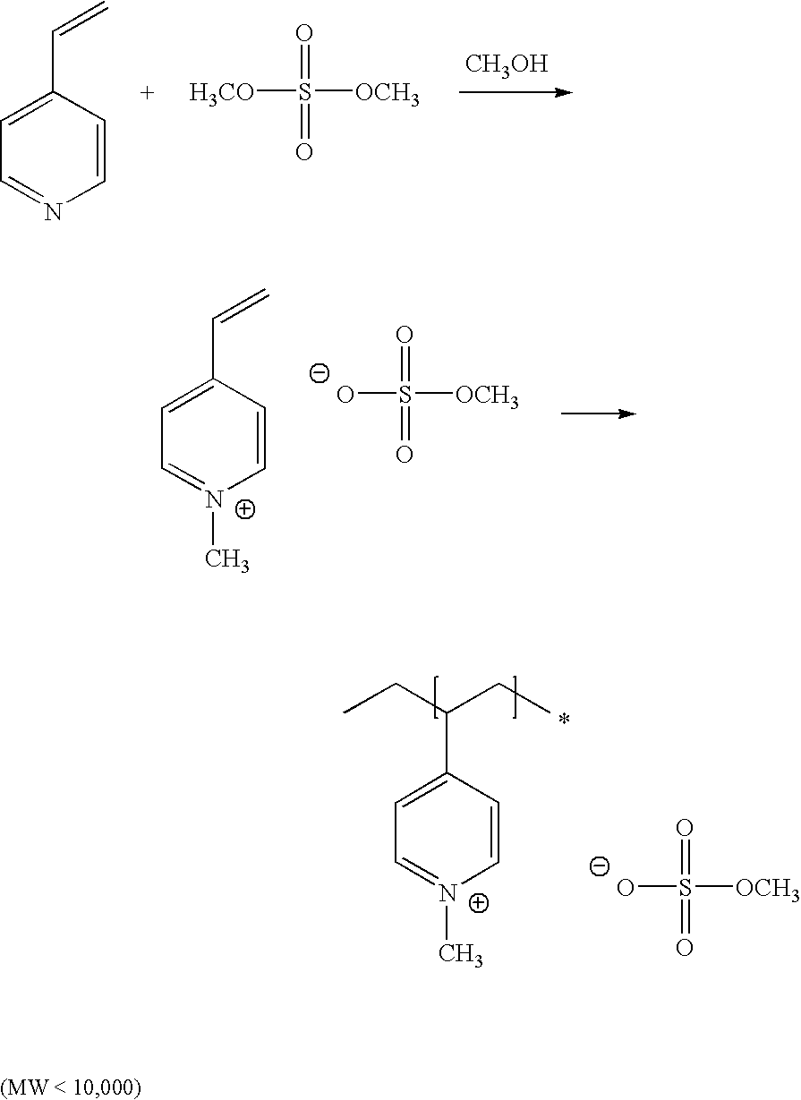
- 4-vinyl pyridine is quaternized by reaction with dimethyl sulfate, and spontaneous polymerization occurs according to the following reaction scheme (45-65° C.):
- the monomer fraction is increased with an increase in amount of methanol used in the quaternization reaction; that is, the degree of spontaneous polymerization is decreased.
- the component that polarizes the copper deposition and renders a slower copper deposition rate near the opening of a via feature may be incorporated into the electroplating bath at concentrations between about 1 ppm and about 200 ppm.
- the component that suppresses the rate of copper deposition near the opening of a via feature may be added to the electrolytic copper deposition composition at concentrations between about 1 and about 40 ppm or higher, preferably between about 2 ppm and about 20 ppm.
- concentration of the component is optimally determined in view of the aspect ratio of the feature to be copper metallized.
- the concentration of the component is preferably near the lower end of the preferred range, such as between about 4.2 ppm and about 8.4 ppm (0.45 micromolar), such as about 5.6 ppm.
- the concentration of the component is preferably near the higher end of the preferred range, such as between about 9.8 ppm and about 14 ppm, such as about 11.2 ppm.
- the leveler concentration is preferably maintained near the lower end of the preferred range to avoid unnecessarily prolonging the fill time.
- PPGA polypropylene glycol amine
- PPG low molecular weight polypropylene glycol
- the electrolytic baths include acid baths including mixed organic acid baths and alkaline baths.
- Exemplary electrolytic copper plating baths include copper fluoroborate, copper pyrophosphate, copper phosphonate, copper sulfate, and other copper metal complexes such as copper methane sulfonate.
- Preferred copper sources include copper sulfate in sulfuric acid solution and copper methane sulfonate in methane sulfonic acid solution.
- the copper source is copper methanesulfonate and the acid is methanesulfonic acid.
- the use of copper methanesulfonate as the copper source allows for greater concentrations of copper ions in the electrolytic copper deposition composition in comparison to other copper ion sources. Accordingly, the source of copper ion may be added to achieve copper ion concentrations greater than about 50 g/L, greater than about 90 g/L, or even greater than about 100 g/L, such as, for example about 110 g/L.
- the copper methane sulfonate is added to achieve a copper ion concentration between about 70 g/L and about 100 g/L.
- the copper concentration is optimally determined in view of the aspect ratio of the feature to be copper metallized.
- the concentration of the copper ion is added and maintained at the higher end of the preferred concentration range, such as between about 90 g/L and about 110 g/L, such as about 110 g/L.
- the concentration of the copper ion may be added and maintained at the lower end of the preferred concentration range, such as between about 80 g/L and about 100 g/L, such as about 90 g/L.
- the concentration of the copper ion is optimally decreased.
- the copper concentration may be increased in embodiments wherein the feature a relatively low aspect ratio.
- methane sulfonic acid and its derivative and other organic sulfonic acids as the electrolyte.
- methane sulfonic acid When methane sulfonic acid is added, its concentration may be between about 1 g/L and about 50 g/L, such as between about 5 g/L and about 25 g/L, such as about 20 g/L.
- Experimental evidence to date indicates that increased acidity advantageously plays a role in the copper metallization process.
- incorporating methane sulfonic acid in the electrolytic copper deposition composition reduces the electrochemical copper reduction potential (i.e., makes it less negative, thereby facilitating Cu deposition, as shown in FIG. 6 .
- FIG. 6 shows three current-potential curves from cyclic voltammetric experiments, with MSA concentrations of 0, 2 g/L, and 4 g/L. In this experiment, both copper reduction and oxidation information were obtained. It is important to distinguish the anodic current and cathodic current. In plating terminology, when the current is positive (I>0), it is called anodic current; when the current is negative (I ⁇ 0), it is called cathodic current or reduction current. Attention is paid to the cathodic behavior or reduction of Cu(II) to Cu metal (lower left curves). As it is shown clearly in FIG.
- the concentration of copper ion and acid may vary over wide limits; for example, from about 4 to about 70 g/L copper and from about 2 to about 225 g/L sulfuric acid.
- the compounds of the invention are suitable for use in distinct acid/copper concentration ranges, such as high acid/low copper systems, in low acid/high copper systems, and mid acid/high copper systems.
- the copper ion concentration can be on the order of 4 g/L to on the order of 30 g/L; and the acid concentration may be sulfuric acid in an amount of greater than about 100 g/L up to about 225 g/L.
- the copper ion concentration is about 17 g/L where the H 2 SO 4 concentration is about 180 g/L.
- the copper ion concentration can be between about 35 g/L and about 60 g/L, such as between about 38 g/L and about 42 g/L.
- the copper ion concentration can be between about 46 g/L and about 60 g/L, such as between about 48 g/L and about 52 g/L. (35 g/L copper ion corresponds to about 140 g/L CuSO4.5H2O copper sulfate pentahydrate.)
- the acid concentration in these systems is preferably less than about 100 g/L.
- the acid concentration can be between about 5 g/L and about 30 g/L, such as between about 10 g/L and about 15 g/L. In some low acid/high copper, the acid concentration can be between about 50 g/L and about 100 g/L, such as between about 75 g/L to about 85 g/L. In an exemplary low acid/high copper system, the copper ion concentration is about 40 g/L and the H 2 SO 4 concentration is about 10 g/L. In another exemplary low acid/high copper system, the copper ion concentration is about 50 g/L and the H 2 SO 4 concentration is about 80 g/L.
- the copper ion concentration can be on the order of 30 g/L to on the order of 60 g/L; and the acid concentration may be sulfuric acid in an amount of greater than about 50 g/L up to about 100 g/L. In one mid acid/high copper system, the copper ion concentration is about 50 g/L where the H 2 SO 4 concentration is about 80 g/L.
- Chloride ion may also be used in the bath at a level up to about 200 mg/L (about 200 ppm), preferably about 10 mg/L to about 90 mg/L (10 to 90 ppm), such as about 50 gm/L (about 50 ppm). Chloride ion is added in these concentration ranges to enhance the function of other bath additives. In particular, it has been discovered that the addition of chloride ion enhances void-free filling.
- FIG. 7 is a flow chart of the process steps in preparing a wafer-to-wafer stack or chip-to-wafer stack involving through silicon via metallization.
- the wafer substrate i.e., device wafer
- the electrolytic copper deposition solution of the present invention comprises a back surface, a front surface, and vias and through silicon vias, which are prepared by photolithography and etching methods as is conventionally known.
- the front surface refers to the active side of the device wafer substrate.
- vias and through silicon vias have openings that extend from the front surface of the wafer substrate to a depth defined by the length of their sidewalls.
- conventional photoresist material is applied to a cleaned and dried surface of a device wafer by spin coating.
- the photoresist may be soft-baked to remove excess solvent at a temperature between about 60° C. and about 100° C. for about 5 to 30 minutes.
- the photoresist is exposed to ultraviolet light in a manner that defines the pattern of copper metallization.
- Exposed photoresist is then dissolved using a developer solution.
- the wafer and photoresist defining the copper metallization pattern is then hard-baked, typically between about 120° C. and about 180° C. for about 20 to 30 minutes.
- the exposed wafer is then etched by means known in the art to define a pattern of vias having sidewalls and bottoms.
- the front surface of the wafer substrate and the sidewalls and the bottoms of the vias are then coated with a barrier layer, which may be titanium nitride, tantalum, tantalum nitride, or ruthenium to inhibit copper diffusion.
- a barrier layer which may be titanium nitride, tantalum, tantalum nitride, or ruthenium to inhibit copper diffusion.
- the barrier layer is typically seeded with a seed layer of copper or other metal to initiate copper superfilling plating thereon.
- a copper seed layer may be applied by chemical vapor deposition (CVD), physical vapor deposition (PVD), or the like.
- CVD chemical vapor deposition
- PVD physical vapor deposition
- the vias having barrier layers and copper seed layers are then plated using the electrolytic copper deposition composition and method of the present invention.
- the wafer surface having TSV features therein may optionally be pretreated to ensure proper wetting of the vias with the Cu filling chemistry.
- An exemplary solution useful for degassing the wafer surface if MICROFAB® PW 1000, available from Enthone Inc. (West Haven, Conn.). After degassing, TSV features located in the wafer is copper metallized using the electrolytic copper deposition composition of the present invention.
- a cathode substrate and anode are electrically connected by wiring and, respectively, to a rectifier (power supply).
- the cathode substrate for direct or pulse current has a net negative charge so that copper ions in the solution are reduced at the cathode substrate forming plated copper metal on the cathode surface.
- An oxidation reaction takes place at the anode. This same oxidation reaction may take place at the cathode if periodic pulse reverse plating is used.
- the cathode and anode may be horizontally or vertically disposed in the tank.
- a pulse current, direct current, reverse periodic current, periodic pulse reverse current, step current or other suitable current may be employed.
- the temperature of the electrolytic solution may be maintained using a heater/cooler whereby electrolytic solution is removed from the holding tank and flows through the heater/cooler and then is recycled to the holding tank.
- the bath temperature is typically about room temperature such as about 20-27° C., but may be at elevated temperatures up to about 40° C. or higher. It is preferred to use an anode to cathode ratio of about 1:1, but this may also vary widely from about 1:4 to 4:1.
- the process also uses mixing in the electrolytic plating tank which may be supplied by agitation or preferably by the circulating flow of recycle electrolytic solution through the tank.
- use of the methane sulfonic acid based electrolytic copper deposition composition containing the preferred polarizing and/or depolarizing additives of the present invention allows for enhanced filling growth rates, as shown in FIG. 1 .
- the method of the present invention employs a current density profile in which initiation preferably occurs at a relatively low current density and in which the current density is increased after a period of copper deposition.
- Relatively low current densities may be used initially typically to avoid depleting copper ion locally near the bottom of the feature faster than the copper ion may be replenished. A situation wherein the depletion rate is faster than the replenishment rate may lead to the formation of a void.
- Optimal initial current densities and durations are typically determined experimentally and may vary depending upon the aspect ratio of the through silicon via feature. Increasing the initial relatively low current density to a relatively higher final current density may be continuous or according to a stepped profile.
- the current density may be stepped from an initiating current density to a second current density and stepped again to a final maximum current density.
- there may be more than two current density steps such as three, four, five, or more current density steps.
- Overall the current density averages between about 0.3 A/dm 2 and about 3 A/dm 2 .
- An exemplary stepped current density profile according to the method of the present invention may be as follows:
- the increase in current density in each step may be about 0.1 A/dm 2 , about 0.2 A/dm 2 , about 0.3 A/dm 2 , about 0.4 A/dm 2 , or more.
- the wafer surface and exposed copper metallization may be cleaned by chemical mechanical polishing, as is known in the art.
- the wafer may be thinned by conventional etching techniques to expose the bottom layer of copper metallization, thereby achieving through silicon via wherein copper metallization extends from the back surface of the wafer or IC die to the front, active surface of the wafer or die.
- the wafer may be further processed, stacked, and singulated by methods known in the art to achieve a device comprising multiple device levels, each connected electronically using through silicon via.
- An electrolytic copper deposition composition according to the present invention was prepared comprising the following components:
- Cu(CH 3 SO 3 )2 (copper methane sulfonate sufficient to yield 100 g/L copper ions)
- MICROVAB DVF 200 Additive C available from Enthone Inc., West Haven, Conn. (4 mL/L) containing methyl quaternized poly(vinyl-4-pyridine).
- the vias had an aspect ratio of 2.5:1 (depth:opening diameter), resulting from an opening having a diameter of 100 microns and a total depth of 250 microns.
- the current density profile was characterized by relatively rapid increases to a maximum current density of 0.60 A/dm 2 .
- the test wafer was degassed using MICROFAB® PW 1000 (available from Enthone Inc., West Haven, Conn.) and then immersed in the electrolytic copper deposition composition.
- the anode was a copper anode that was filmed prior to use in a copper methane sulfonate plating bath.
- the power supply supplied an average current density of 0.57 A/dm 2 .
- the current density was supplied according to the following stepped profile:
- FIGS. 8A and 8B are cross sections of the completely filled TSV features. Plating appears to occur according to a bottom-up mechanism since the TSV were void-free and seam-free.
- An electrolytic copper deposition composition according to the present invention was prepared comprising the following components:
- the vias had an aspect ratio of 1.75:1; 2.16:1; 3:1; and 5:1 (depth:opening diameter), resulting from an opening having the following diameters, respectively: 40, 30, 20, 10 microns, and the following depths, respectively: 70, 65, 60, 50 microns.
- the current density profile was characterized by relatively rapid increases to a maximum current density of 1.4 A/dm 2 .
- the test wafer was degassed using MICROFAB® PW 1000 (available from Enthone Inc., West Haven, Conn.) and then immersed in the electrolytic copper deposition composition.
- the anode was a copper anode that was filmed prior to use in a copper methane sulfonate plating bath.
- the power supply supplied an average current density of 0.84 A/dm 2 .
- the current density was supplied according to the following stepped profile:
- FIGS. 9A , B, C, and D are FIB (Focused Ion Beam) cross sections of the completely filled TSV features. Plating appears to occur according to a bottom-up mechanism since the TSV were void-free and seam-free.
- An electrolytic copper deposition composition according to the present invention was prepared comprising the following components:
- Polypropylene glycol amine (ca. 400 g/mol) 30 mg/L
- the vias had an aspect ratio of 3.5:1; 3.8:1; 2.5:1; and 5:1 (depth:opening diameter), resulting from an opening having the following diameters respectively: 50; 45; 75; 35 microns; and all having a depth of 175 microns.
- the current density profile was characterized by relatively rapid increases to a maximum current density of 1.2 A/dm 2 .
- the test wafer was degassed using MICROFAB® PW 1000 (available from Enthone Inc., West Haven, Conn.) and then immersed in the electrolytic copper deposition composition.
- the anode was a copper anode that was filmed prior to use in a copper methane sulfonate plating bath.
- the power supply supplied an average current density of 0.93 A/dm 2 .
- the current density was supplied according to the following stepped profile:
- FIGS. 10A , B, C, and D are optical cross sections of the completely filled TSV features. Plating appears to occur according to a bottom-up mechanism since the TSV were void-free and seam-free.
- An electrolytic copper deposition composition having a composition:
- An electrolytic copper deposition composition according to the present invention was prepared comprising the following components:
- Polypropylene gycol amine (ca. 400 g/mol; 30 mg/L)
- the vias had an aspect ratio of 3.5:1; 2.5:1 (depth:opening diameter), resulting from an opening having the following diameters respectively: 50; 75 microns; and each having a depth of 175 microns.
- the current density profile was characterized by relatively rapid increases to a maximum current density of 1.2 A/dm 2 .
- the test wafer was degassed using MICROFAB® PW 1000 (available from Enthone Inc., West Haven, Conn.) and then immersed in the electrolytic copper deposition composition.
- the anode was a copper anode that was filmed prior to use in a copper methane sulfonate plating bath.
- the power supply supplied an average current density of 0.93 A/dm 2 .
- the current density was supplied according to the following stepped profile:
- FIGS. 11A and B are optical cross sections of the completely filled TSV features. Plating appears to occur according to a bottom-up mechanism since the TSV were void-free and seam-free.
- An electrolytic copper deposition composition according to the present invention was prepared comprising the following components:
- Synalox 40-D700 (0.2 g/L) (random EO/PO copolymer available from Dow Chemical; m.w. 5300)
- the electrolytic copper deposition composition of Example 5 was used to deposit copper metallization into a large size via in a test wafer substrate.
- the vias had an opening having a diameter of 50 microns and a total depth of 135 microns.
- the test wafer was degassed using MICROFAB® PW 1000 (available from Enthone Inc., West Haven, Conn.) and then immersed in the electrolytic copper deposition composition of Example 5.
- the anode was a copper anode that was filmed prior to use in a copper methane sulfonate plating bath.
- the power supply supplied an average current density of 0.50 A/dm2.
- the current density was supplied according to the following stepped profile:
- FIGS. 12A and 12B are optical photographs (500 ⁇ magnification) of filled TSV features. Plating appears to occur according to a bottom-up mechanism since void-free and seam-free copper filled TSV were obtained.
- An electrolytic copper deposition composition according to the present invention was prepared comprising the following components:
- MICROFAB DVF200 B (3,3′-dithiobis(1-propanesulfonic acid) (6 mL/L)
- MIROFAB DVF200 C Metal quaternized poly(vinyl-4-pyridine) (4 mL/L).
- the electrolytic copper deposition composition of Example 7 was used to deposit copper metallization into a large size via in a test wafer substrate.
- the vias had an opening having a diameter of 50 microns and a total depth of 200 microns.
- the test wafer was degassed using MICROFAB® PW 1000 (available from Enthone Inc., West Haven, Conn.) and then immersed in the electrolytic copper deposition composition of Example 7.
- the anode was a copper anode that was filmed prior to use in a copper methane sulfonate plating bath.
- the power supply supplied an average current density of 0.64 A/dm 2 .
- the current density was supplied according to the following stepped profile:
- FIGS. 13A and 13B are optical photographs (500 ⁇ magnification) of the partially filled TSV features. Plating appears to occur according to a true bottom-up mechanism as indicated by the “U” shaped plating profile.
- the electrolytic copper deposition composition of Example 7 was used to deposit copper metallization into a large size via in a test wafer substrate.
- the vias had an aspect ratio of 3:1 (depth:opening diameter), resulting from an opening having a diameter of 50 microns and a total depth of 150 microns.
- the current density profile was characterized by relatively rapid increases to a maximum current density of 0.60 A/dm 2 .
- the test wafer was degassed using MICROFAB® PW 1000 (available from Enthone Inc., West Haven, Conn.) and then immersed in the electrolytic copper deposition composition of Example 7.
- the anode was a copper anode that was filmed prior to use in a copper methane sulfonate plating bath.
- the power supply supplied an average current density of 0.58 A/dm 2 .
- the current density was supplied according to the following stepped profile:
- FIGS. 14A and 14B are optical photographs (200 ⁇ magnification) of the completely filled TSV features. Plating appears to occur according to a bottom-up mechanism since the TSV were void-free and seam-free.
- An electrolytic copper deposition composition having a composition identical to that of Example 7 except for an increase in the concentration of the methyl quaternized poly(vinyl-4-pyridine) to 8 mL/L was used to deposit copper metallization into a large size, high aspect ratio via in a test wafer substrate.
- the vias had an aspect ratio of 4:1 (depth:opening diameter), resulting from an opening having a diameter of 50 microns and a total depth of 200 microns.
- the current density profile was characterized by relatively rapid increases to a maximum current density of 0.60 A/dm 2 .
- the test wafer was degassed using MICROFAB® PW 1000 (available from Enthone Inc., West Haven, Conn.) and then immersed in the electrolytic copper deposition composition.
- the anode was a copper anode that was filmed prior to use in a copper methane sulfonate plating bath.
- the power supply supplied an average current density of 0.64 A/dm 2 .
- the current density was supplied according to the following stepped profile:
- FIGS. 15A and 15B are optical photographs (200 ⁇ magnification) of the completely filled TSV features. Plating appears to occur according to a bottom-up mechanism since the TSV were void-free and seam-free.
- Electrolytic Copper Deposition Composition Comprising Superfilling Additives
- An electrolytic copper deposition composition comprising superfilling additives was prepared comprising the following components:
- the electrolytic copper deposition composition of Comparative Example 1 was used to deposit copper metallization into a large size via in a test wafer substrate.
- the via had an opening having a diameter of 50 microns and a total depth of 150 microns.
- the current density was relatively low to ensure good initiation, bottom up filling, and defect-free metallization.
- the test wafer was degassed using MICROFAB® PW 1000 (available from Enthone Inc., West Haven, Conn.) and then immersed in the electrolytic copper deposition composition of Comparative Example 1.
- the anode was a copper anode that was filmed prior to use in a copper sulfate plating bath.
- the power supply supplied a current density of 0.11 A/dm 2 and plating was discontinued after five hours.
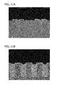
- FIG. 16 is an optical photograph (500 ⁇ magnification) of the partially filled TSV feature. It is apparent from FIG. 16 that 5 hours of plating at this current density was not sufficient to metallize the entire feature. In fact, the feature was only about 33% filled.
- Electrolytic Copper Deposition Composition Comprising Superfilling Additives
- An electrolytic copper deposition composition comprising superfilling additives was prepared comprising the following components:
- the electrolytic copper deposition composition of Comparative Example 3 was used to deposit copper metallization into a large size via in a test wafer substrate.
- the via had an opening having a diameter of 50 microns and a total depth of 150 microns.
- the current density was relatively low to ensure good initiation, bottom up filling, and defect-free metallization.
- the test wafer was degassed using MICROFAB® PW 1000 (available from Enthone Inc., West Haven, Conn.) and then immersed in the electrolytic copper deposition composition of Comparative Example 3.
- the anode was a copper anode that was filmed prior to use in a copper sulfate plating bath.
- the power supply supplied a current density of 0.11 A/dm 2 and plating continued until the feature was completely filled with copper metal.
- FIG. 17 is an optical photograph (500 ⁇ magnification) of the filled TSV feature. Deposition was characterized by bottom up growth, and the metallization was void-free and defect-free. The plating rate in the vertical direction was very slow however, about 0.27 microns/minute, and although the metallized feature was defect-free, filling the entire feature took 10 hours.
Abstract
Description

wherein
- X is O, S, or S═O;
- n is 1 to 6;
- M is hydrogen, alkali metal, or ammonium as needed to satisfy the valence;
- R1 is an alkylene or cyclic alkylene group of 1 to 8 carbon atoms, an aromatic hydrocarbon or an aliphatic aromatic hydrocarbon of 6 to 12 carbon atoms; and
- R2 is hydrogen, hydroxyalkyl having from 1 to 8 carbon atoms, or MO3SR1 wherein M and R1 are as defined above.

wherein M is a counter ion possessing charge sufficient to balance the negative charges on the oxygen atoms. M may be, for example, protons, alkali metal ions such as sodium and potassium, or another charge balancing cation such as ammonium or a quaternary amine.


R1-L (17)
-
- 1. Initiate plating at a current density between about 0.1 A/dm2 and about 0.2 A/dm2 for a duration between about 30 seconds and about 60 min.
- 2. Step the current density to between about 0.3 A/dm2 and about 0.5 A/dm2 and maintaining the current density after each step for a duration between about 1 min and about 60 min. This may involve one or more than one step, such as a step to 0.3 A/dm2, followed by a step to 0.4 A/dm2, followed by a step to about 0.5 A/dm2.
- 3. Step the current density to the final current density of between about 0.6 A/dm2 and about 1.2 A/dm2 and maintaining the current density after each step for a duration between about 60 min and about 90 min. This may involve one or more than one step, such as a step to 0.6 A/dm2, followed by a step to 0.7 A/dm2, followed by a step to about 0.8 A/dm2, followed by a step to about 0.9 A/dm2, followed by a step to about 1.0 A/dm2, followed by a step to about 1.1 A/dm2, followed by a step to about 1.2 A/dm2.
Claims (21)

Priority Applications (1)
| Application Number | Priority Date | Filing Date | Title |
|---|---|---|---|
| US12/185,641 US7670950B2 (en) | 2007-08-02 | 2008-08-04 | Copper metallization of through silicon via |
Applications Claiming Priority (3)
| Application Number | Priority Date | Filing Date | Title |
|---|---|---|---|
| US95360207P | 2007-08-02 | 2007-08-02 | |
| US5903908P | 2008-06-05 | 2008-06-05 | |
| US12/185,641 US7670950B2 (en) | 2007-08-02 | 2008-08-04 | Copper metallization of through silicon via |
Publications (2)
| Publication Number | Publication Date |
|---|---|
| US20090035940A1 US20090035940A1 (en) | 2009-02-05 |
| US7670950B2 true US7670950B2 (en) | 2010-03-02 |
Family
ID=40304935
Family Applications (1)
| Application Number | Title | Priority Date | Filing Date |
|---|---|---|---|
| US12/185,641 Active US7670950B2 (en) | 2007-08-02 | 2008-08-04 | Copper metallization of through silicon via |
Country Status (7)
| Country | Link |
|---|---|
| US (1) | US7670950B2 (en) |
| EP (1) | EP2183769B8 (en) |
| JP (1) | JP2010535289A (en) |
| KR (1) | KR101529342B1 (en) |
| CN (1) | CN101855714B (en) |
| TW (1) | TWI341554B (en) |
| WO (1) | WO2009018581A1 (en) |
Cited By (24)
| Publication number | Priority date | Publication date | Assignee | Title |
|---|---|---|---|---|
| US20100200412A1 (en) * | 2008-08-18 | 2010-08-12 | Novellus Systems, Inc. | Process For Through Silicon Via Filling |
| US20100264551A1 (en) * | 2009-04-20 | 2010-10-21 | International Business Machines Corporation | Three dimensional integrated circuit integration using dielectric bonding first and through via formation last |
| US20100320081A1 (en) * | 2009-06-17 | 2010-12-23 | Mayer Steven T | Apparatus for wetting pretreatment for enhanced damascene metal filling |
| WO2012103357A1 (en) | 2011-01-26 | 2012-08-02 | Enthone Inc. | Process for filling vias in the microelectronics |
| US8404588B2 (en) | 2010-10-06 | 2013-03-26 | Electronics And Telecommunications Research Institute | Method of manufacturing via electrode |
| US20130178063A1 (en) * | 2012-01-11 | 2013-07-11 | United Microelectronics Corp. | Method of manufacturing semiconductor device having silicon through via |
| US8563403B1 (en) | 2012-06-27 | 2013-10-22 | International Business Machines Corporation | Three dimensional integrated circuit integration using alignment via/dielectric bonding first and through via formation last |
| US8992757B2 (en) | 2010-05-19 | 2015-03-31 | Novellus Systems, Inc. | Through silicon via filling using an electrolyte with a dual state inhibitor |
| US20150214171A1 (en) * | 2014-01-24 | 2015-07-30 | Zhuhai Advanced Chip Carriers & Electronic Substrate Solutions Technologies Co., Ltd. | Substrates with Protruding Copper Termination Posts |
| US9109295B2 (en) | 2009-10-12 | 2015-08-18 | Novellus Systems, Inc. | Electrolyte concentration control system for high rate electroplating |
| US9138784B1 (en) | 2009-12-18 | 2015-09-22 | Novellus Systems, Inc. | Deionized water conditioning system and methods |
| US9190371B2 (en) | 2010-12-21 | 2015-11-17 | Moon J. Kim | Self-organizing network with chip package having multiple interconnection configurations |
| EP2963158A1 (en) | 2014-06-30 | 2016-01-06 | Rohm and Haas Electronic Materials LLC | Plating method |
| US9330975B2 (en) | 2012-05-31 | 2016-05-03 | Micron Technology, Inc. | Integrated circuit substrates comprising through-substrate vias and methods of forming through-substrate vias |
| US9435049B2 (en) | 2013-11-20 | 2016-09-06 | Lam Research Corporation | Alkaline pretreatment for electroplating |
| US9455139B2 (en) | 2009-06-17 | 2016-09-27 | Novellus Systems, Inc. | Methods and apparatus for wetting pretreatment for through resist metal plating |
| US9481942B2 (en) | 2015-02-03 | 2016-11-01 | Lam Research Corporation | Geometry and process optimization for ultra-high RPM plating |
| US9613833B2 (en) | 2013-02-20 | 2017-04-04 | Novellus Systems, Inc. | Methods and apparatus for wetting pretreatment for through resist metal plating |
| US9617648B2 (en) | 2015-03-04 | 2017-04-11 | Lam Research Corporation | Pretreatment of nickel and cobalt liners for electrodeposition of copper into through silicon vias |
| EP3162921A1 (en) | 2015-10-27 | 2017-05-03 | Rohm and Haas Electronic Materials LLC | Method of electroplating copper into a via on a substrate from an acid copper electroplating bath |
| US9677188B2 (en) | 2009-06-17 | 2017-06-13 | Novellus Systems, Inc. | Electrofill vacuum plating cell |
| US10472730B2 (en) | 2009-10-12 | 2019-11-12 | Novellus Systems, Inc. | Electrolyte concentration control system for high rate electroplating |
| US10692735B2 (en) | 2017-07-28 | 2020-06-23 | Lam Research Corporation | Electro-oxidative metal removal in through mask interconnect fabrication |
| WO2020160352A1 (en) | 2019-01-31 | 2020-08-06 | Macdermid Enthone Inc. | Composition and method for fabrication of nickel interconnects |
Families Citing this family (30)
| Publication number | Priority date | Publication date | Assignee | Title |
|---|---|---|---|---|
| US10221496B2 (en) | 2008-11-26 | 2019-03-05 | Macdermid Enthone Inc. | Copper filling of through silicon vias |
| US8388824B2 (en) * | 2008-11-26 | 2013-03-05 | Enthone Inc. | Method and composition for electrodeposition of copper in microelectronics with dipyridyl-based levelers |
| US20100206737A1 (en) * | 2009-02-17 | 2010-08-19 | Preisser Robert F | Process for electrodeposition of copper chip to chip, chip to wafer and wafer to wafer interconnects in through-silicon vias (tsv) |
| US20110042803A1 (en) * | 2009-08-24 | 2011-02-24 | Chen-Fu Chu | Method For Fabricating A Through Interconnect On A Semiconductor Substrate |
| US20120175744A1 (en) | 2009-09-28 | 2012-07-12 | Basf Se | Copper electroplating composition |
| KR101302564B1 (en) * | 2009-10-28 | 2013-09-02 | 한국전자통신연구원 | Method of forming a via and method of fabricating chip stack package thereof |
| KR101300587B1 (en) * | 2009-12-09 | 2013-08-28 | 한국전자통신연구원 | Method for forming semiconductor device |
| JP5384719B2 (en) * | 2010-02-22 | 2014-01-08 | Jx日鉱日石金属株式会社 | High purity copper sulfonate aqueous solution and method for producing the same |
| WO2011154493A1 (en) | 2010-06-11 | 2011-12-15 | Alchimer | Copper-electroplating composition and process for filling a cavity in a semiconductor substrate using this composition |
| US20120024713A1 (en) * | 2010-07-29 | 2012-02-02 | Preisser Robert F | Process for electrodeposition of copper chip to chip, chip to wafer and wafer to wafer interconnects in through-silicon vias (tsv) with heated substrate and cooled electrolyte |
| TW201221703A (en) * | 2010-11-18 | 2012-06-01 | Chiracol Co Ltd | Electrolytic copper plating bath and electrolytic copper plating method used for semiconductor |
| KR101705734B1 (en) * | 2011-02-18 | 2017-02-14 | 삼성전자주식회사 | Copper electroplating solution and method of copper electroplating using the same |
| US8884083B2 (en) | 2011-02-21 | 2014-11-11 | E. I. Du Pont De Nemours And Company | Selective catalytical dehydrochlorination of hydrochlorofluorocarbons |
| EP2518187A1 (en) * | 2011-04-26 | 2012-10-31 | Atotech Deutschland GmbH | Aqueous acidic bath for electrolytic deposition of copper |
| SG194983A1 (en) | 2011-06-01 | 2013-12-30 | Basf Se | Composition for metal electroplating comprising an additive for bottom-up filling of though silicon vias and interconnect features |
| EP2530102A1 (en) | 2011-06-01 | 2012-12-05 | Basf Se | Additive and composition for metal electroplating comprising an additive for bottom-up filling of though silicon vias |
| EP2560196A1 (en) | 2011-08-15 | 2013-02-20 | Nederlandse Organisatie voor toegepast -natuurwetenschappelijk onderzoek TNO | Method and system for forming a metallic structure |
| CN102443828B (en) * | 2011-09-23 | 2014-11-19 | 上海华力微电子有限公司 | Method for electro-coppering in through hole of semiconductor silicon chip |
| US8383460B1 (en) * | 2011-09-23 | 2013-02-26 | GlobalFoundries, Inc. | Method for fabricating through substrate vias in semiconductor substrate |
| CN103839872A (en) * | 2012-11-21 | 2014-06-04 | 中芯国际集成电路制造(上海)有限公司 | Method for manufacturing semiconductor device |
| CN103290438B (en) * | 2013-06-25 | 2015-12-02 | 深圳市创智成功科技有限公司 | For copper electroplating solution and the electro-plating method of wafer-level packaging |
| CN103361694A (en) * | 2013-08-08 | 2013-10-23 | 上海新阳半导体材料股份有限公司 | Micro-pore electroplated copper filling method for three-dimensional (3D) copper interconnection high aspect ratio through-silicon-via technology |
| CN103397354B (en) * | 2013-08-08 | 2016-10-26 | 上海新阳半导体材料股份有限公司 | A kind of additive in cavity after reducing silicon through hole technology copper facing annealing |
| US20160348245A1 (en) * | 2015-05-28 | 2016-12-01 | Macdermid, Incorporated | Method of Pretreatment for Electroless Plating |
| KR102448669B1 (en) | 2015-06-30 | 2022-09-29 | 맥더미드 엔쏜 인코포레이티드 | Cobalt filling of interconnects in microelectronics |
| WO2017090161A1 (en) * | 2015-11-26 | 2017-06-01 | 近藤 和夫 | Acidic copper plating solution, acidic copper plated product, and method for producing semiconductor device |
| US11035048B2 (en) | 2017-07-05 | 2021-06-15 | Macdermid Enthone Inc. | Cobalt filling of interconnects |
| US10566287B1 (en) * | 2018-02-02 | 2020-02-18 | Inphi Corporation | Light engine based on silicon photonics TSV interposer |
| US11387191B2 (en) * | 2019-07-18 | 2022-07-12 | Taiwan Semiconductor Manufacturing Company, Ltd. | Integrated circuit package and method |
| US11165509B1 (en) | 2020-06-05 | 2021-11-02 | Marvell Asia Pte, Ltd. | Method for co-packaging light engine chiplets on switch substrate |
Citations (44)
| Publication number | Priority date | Publication date | Assignee | Title |
|---|---|---|---|---|
| US4110176A (en) | 1975-03-11 | 1978-08-29 | Oxy Metal Industries Corporation | Electrodeposition of copper |
| US4389505A (en) | 1981-12-16 | 1983-06-21 | Mobil Oil Corporation | Plasticized polyacrylonitrile, a film thereof and a process for film preparation and plasticization |
| US20020112964A1 (en) | 2000-07-12 | 2002-08-22 | Applied Materials, Inc. | Process window for gap-fill on very high aspect ratio structures using additives in low acid copper baths |
| US6444110B2 (en) | 1999-05-17 | 2002-09-03 | Shipley Company, L.L.C. | Electrolytic copper plating method |
| US6518182B1 (en) | 1999-11-12 | 2003-02-11 | Ebara-Udylite Co., Ltd. | Via-filling process |
| US6544399B1 (en) | 1999-01-11 | 2003-04-08 | Applied Materials, Inc. | Electrodeposition chemistry for filling apertures with reflective metal |
| US6551487B1 (en) | 2001-05-31 | 2003-04-22 | Novellus Systems, Inc. | Methods and apparatus for controlled-angle wafer immersion |
| US6607654B2 (en) | 2000-09-27 | 2003-08-19 | Samsung Electronics Co., Ltd. | Copper-plating elecrolyte containing polyvinylpyrrolidone and method for forming a copper interconnect |
| US6610191B2 (en) | 1998-04-21 | 2003-08-26 | Applied Materials, Inc. | Electro deposition chemistry |
| US6638411B1 (en) | 1999-01-26 | 2003-10-28 | Ebara Corporation | Method and apparatus for plating substrate with copper |
| US6660153B2 (en) | 2000-10-20 | 2003-12-09 | Shipley Company, L.L.C. | Seed layer repair bath |
| US20040045832A1 (en) | 1999-10-14 | 2004-03-11 | Nicholas Martyak | Electrolytic copper plating solutions |
| US6706418B2 (en) | 2000-07-01 | 2004-03-16 | Shipley Company L.L.C. | Metal alloy compositions and plating methods related thereto |
| US20040082756A1 (en) * | 2002-06-27 | 2004-04-29 | Recai Sezi | Poly-o-hydroxyamide, polybenzoxazole from the poly-o-hydroxyamide, electronic component including a polybenzoxazole, and processes for producing the same |
| US6740221B2 (en) | 2001-03-15 | 2004-05-25 | Applied Materials Inc. | Method of forming copper interconnects |
| US6747217B1 (en) | 2001-11-20 | 2004-06-08 | Unisys Corporation | Alternative to through-hole-plating in a printed circuit board |
| US20040154926A1 (en) | 2002-12-24 | 2004-08-12 | Zhi-Wen Sun | Multiple chemistry electrochemical plating method |
| US6776893B1 (en) | 2000-11-20 | 2004-08-17 | Enthone Inc. | Electroplating chemistry for the CU filling of submicron features of VLSI/ULSI interconnect |
| US6793796B2 (en) | 1998-10-26 | 2004-09-21 | Novellus Systems, Inc. | Electroplating process for avoiding defects in metal features of integrated circuit devices |
| US6797142B2 (en) | 2001-05-24 | 2004-09-28 | Shipley Company, L.L.C. | Tin plating |
| US20040217009A1 (en) | 2002-11-21 | 2004-11-04 | Shipley Company, L.L.C. | Electroplating bath |
| US20040222104A1 (en) | 2003-02-19 | 2004-11-11 | Rohm And Haas Electronic Materials, L.L.C | Electroplating composition |
| US20050045488A1 (en) | 2002-03-05 | 2005-03-03 | Enthone Inc. | Copper electrodeposition in microelectronics |
| US6881319B2 (en) | 2000-12-20 | 2005-04-19 | Shipley Company, L.L.C. | Electrolytic copper plating solution and method for controlling the same |
| US20050081744A1 (en) | 2003-10-16 | 2005-04-21 | Semitool, Inc. | Electroplating compositions and methods for electroplating |
| US6924551B2 (en) | 2003-05-28 | 2005-08-02 | Intel Corporation | Through silicon via, folded flex microelectronic package |
| US6926922B2 (en) | 2002-04-09 | 2005-08-09 | Shipley Company, L.L.C. | PWB manufacture |
| US20050199507A1 (en) | 2004-03-09 | 2005-09-15 | Taiwan Semiconductor Manufacturing Co., Ltd. | Chemical structures and compositions of ECP additives to reduce pit defects |
| US20050211564A1 (en) | 2004-03-29 | 2005-09-29 | Taiwan Semiconductor Manufacturing Co., Ltd. | Method and composition to enhance wetting of ECP electrolyte to copper seed |
| US20050241946A1 (en) | 2003-12-25 | 2005-11-03 | Mizuki Nagai | Plating apparatus and plating method |
| US20050274622A1 (en) | 2004-06-10 | 2005-12-15 | Zhi-Wen Sun | Plating chemistry and method of single-step electroplating of copper on a barrier metal |
| US20060076661A1 (en) | 2003-12-17 | 2006-04-13 | Sergey Savastiouk | Attachment of integrated circuit structures and other substrates to substrates with vias |
| US7081408B2 (en) | 2004-10-28 | 2006-07-25 | Intel Corporation | Method of creating a tapered via using a receding mask and resulting structure |
| US7105082B2 (en) | 2003-02-27 | 2006-09-12 | Novellus Systems, Inc. | Composition and method for electrodeposition of metal on a work piece |
| US7111149B2 (en) | 2003-07-07 | 2006-09-19 | Intel Corporation | Method and apparatus for generating a device ID for stacked devices |
| US20060264029A1 (en) | 2005-05-23 | 2006-11-23 | Intel Corporation | Low inductance via structures |
| US20060278979A1 (en) | 2005-06-09 | 2006-12-14 | Intel Corporation | Die stacking recessed pad wafer design |
| US20070001266A1 (en) | 2005-06-30 | 2007-01-04 | Leonel Arana | Integrated circuit die containing particle-filled through-silicon metal vias with reduced thermal expansion |
| US20070085198A1 (en) | 2005-10-13 | 2007-04-19 | Wei Shi | Integrated micro-channels for 3D through silicon architectures |
| US20070235343A1 (en) * | 2006-04-05 | 2007-10-11 | James Watkowski | Process for electrolytically plating copper |
| US7303992B2 (en) | 2004-11-12 | 2007-12-04 | Enthone Inc. | Copper electrodeposition in microelectronics |
| US7316772B2 (en) | 2002-03-05 | 2008-01-08 | Enthone Inc. | Defect reduction in electrodeposited copper for semiconductor applications |
| US7317256B2 (en) | 2005-06-01 | 2008-01-08 | Intel Corporation | Electronic packaging including die with through silicon via |
| US7410884B2 (en) | 2005-11-21 | 2008-08-12 | Intel Corporation | 3D integrated circuits using thick metal for backside connections and offset bumps |
Family Cites Families (13)
| Publication number | Priority date | Publication date | Assignee | Title |
|---|---|---|---|---|
| AU3143500A (en) * | 1999-01-21 | 2000-08-07 | Atotech Deutschland Gmbh | Method for galvanically forming conductor structures of high-purity copper in the production of integrated circuits |
| JP2001181889A (en) * | 1999-12-22 | 2001-07-03 | Nippon Macdermid Kk | Bright tin-copper alloy electroplating bath |
| DE10013801A1 (en) * | 2000-03-20 | 2001-10-18 | Reinhardt Gmbh Maschbau | Sheet metal forming machine |
| JP2003328180A (en) * | 2002-05-17 | 2003-11-19 | Denso Corp | Method of filling plating into bottomed hole |
| US7147767B2 (en) * | 2002-12-16 | 2006-12-12 | 3M Innovative Properties Company | Plating solutions for electrochemical or chemical deposition of copper interconnects and methods therefor |
| JP2005033116A (en) * | 2003-07-11 | 2005-02-03 | Sony Corp | Via hole, semiconductor device having via hole, and forming method of same via hole |
| JP4624738B2 (en) * | 2003-08-21 | 2011-02-02 | 株式会社荏原製作所 | Plating equipment |
| CN1918327B (en) * | 2003-12-22 | 2010-08-25 | 恩索恩公司 | Copper electrodeposition in microelectronics |
| DE102004029894B3 (en) * | 2004-06-17 | 2005-12-22 | Atotech Deutschland Gmbh | Apparatus and method for the electrolytic treatment of electrically mutually insulated, electrically conductive structures on surfaces of flat material to be treated |
| JP4369348B2 (en) * | 2004-11-08 | 2009-11-18 | 新光電気工業株式会社 | Substrate and manufacturing method thereof |
| US7405671B2 (en) * | 2005-07-01 | 2008-07-29 | Sebescak Andrew J | Power failure alarm |
| TWI328622B (en) * | 2005-09-30 | 2010-08-11 | Rohm & Haas Elect Mat | Leveler compounds |
| US20070178697A1 (en) * | 2006-02-02 | 2007-08-02 | Enthone Inc. | Copper electrodeposition in microelectronics |
-
2008
- 2008-08-01 TW TW097129380A patent/TWI341554B/en active
- 2008-08-04 EP EP08797141.2A patent/EP2183769B8/en active Active
- 2008-08-04 CN CN2008801097952A patent/CN101855714B/en active Active
- 2008-08-04 KR KR1020107004714A patent/KR101529342B1/en active IP Right Grant
- 2008-08-04 WO PCT/US2008/072136 patent/WO2009018581A1/en active Application Filing
- 2008-08-04 US US12/185,641 patent/US7670950B2/en active Active
- 2008-08-04 JP JP2010519274A patent/JP2010535289A/en active Pending
Patent Citations (47)
| Publication number | Priority date | Publication date | Assignee | Title |
|---|---|---|---|---|
| US4110176A (en) | 1975-03-11 | 1978-08-29 | Oxy Metal Industries Corporation | Electrodeposition of copper |
| US4389505A (en) | 1981-12-16 | 1983-06-21 | Mobil Oil Corporation | Plasticized polyacrylonitrile, a film thereof and a process for film preparation and plasticization |
| US6610191B2 (en) | 1998-04-21 | 2003-08-26 | Applied Materials, Inc. | Electro deposition chemistry |
| US6793796B2 (en) | 1998-10-26 | 2004-09-21 | Novellus Systems, Inc. | Electroplating process for avoiding defects in metal features of integrated circuit devices |
| US6544399B1 (en) | 1999-01-11 | 2003-04-08 | Applied Materials, Inc. | Electrodeposition chemistry for filling apertures with reflective metal |
| US6596151B2 (en) | 1999-01-11 | 2003-07-22 | Applied Materials, Inc. | Electrodeposition chemistry for filling of apertures with reflective metal |
| US6638411B1 (en) | 1999-01-26 | 2003-10-28 | Ebara Corporation | Method and apparatus for plating substrate with copper |
| US6444110B2 (en) | 1999-05-17 | 2002-09-03 | Shipley Company, L.L.C. | Electrolytic copper plating method |
| US20040045832A1 (en) | 1999-10-14 | 2004-03-11 | Nicholas Martyak | Electrolytic copper plating solutions |
| US6518182B1 (en) | 1999-11-12 | 2003-02-11 | Ebara-Udylite Co., Ltd. | Via-filling process |
| US6706418B2 (en) | 2000-07-01 | 2004-03-16 | Shipley Company L.L.C. | Metal alloy compositions and plating methods related thereto |
| US20020112964A1 (en) | 2000-07-12 | 2002-08-22 | Applied Materials, Inc. | Process window for gap-fill on very high aspect ratio structures using additives in low acid copper baths |
| US6607654B2 (en) | 2000-09-27 | 2003-08-19 | Samsung Electronics Co., Ltd. | Copper-plating elecrolyte containing polyvinylpyrrolidone and method for forming a copper interconnect |
| US6660153B2 (en) | 2000-10-20 | 2003-12-09 | Shipley Company, L.L.C. | Seed layer repair bath |
| US6776893B1 (en) | 2000-11-20 | 2004-08-17 | Enthone Inc. | Electroplating chemistry for the CU filling of submicron features of VLSI/ULSI interconnect |
| US6881319B2 (en) | 2000-12-20 | 2005-04-19 | Shipley Company, L.L.C. | Electrolytic copper plating solution and method for controlling the same |
| US6740221B2 (en) | 2001-03-15 | 2004-05-25 | Applied Materials Inc. | Method of forming copper interconnects |
| US6797142B2 (en) | 2001-05-24 | 2004-09-28 | Shipley Company, L.L.C. | Tin plating |
| US6551487B1 (en) | 2001-05-31 | 2003-04-22 | Novellus Systems, Inc. | Methods and apparatus for controlled-angle wafer immersion |
| US6747217B1 (en) | 2001-11-20 | 2004-06-08 | Unisys Corporation | Alternative to through-hole-plating in a printed circuit board |
| US20050045488A1 (en) | 2002-03-05 | 2005-03-03 | Enthone Inc. | Copper electrodeposition in microelectronics |
| US7316772B2 (en) | 2002-03-05 | 2008-01-08 | Enthone Inc. | Defect reduction in electrodeposited copper for semiconductor applications |
| US6926922B2 (en) | 2002-04-09 | 2005-08-09 | Shipley Company, L.L.C. | PWB manufacture |
| US20040082756A1 (en) * | 2002-06-27 | 2004-04-29 | Recai Sezi | Poly-o-hydroxyamide, polybenzoxazole from the poly-o-hydroxyamide, electronic component including a polybenzoxazole, and processes for producing the same |
| US7244803B2 (en) | 2002-06-27 | 2007-07-17 | Infineon Technologies Ag | Poly-o-hydroxyamide, polybenzoxazole from the poly-o-hydroxyamide, electronic component including a polybenzoxazole, and processes for producing the same |
| US20040217009A1 (en) | 2002-11-21 | 2004-11-04 | Shipley Company, L.L.C. | Electroplating bath |
| US20040154926A1 (en) | 2002-12-24 | 2004-08-12 | Zhi-Wen Sun | Multiple chemistry electrochemical plating method |
| US20040222104A1 (en) | 2003-02-19 | 2004-11-11 | Rohm And Haas Electronic Materials, L.L.C | Electroplating composition |
| US7105082B2 (en) | 2003-02-27 | 2006-09-12 | Novellus Systems, Inc. | Composition and method for electrodeposition of metal on a work piece |
| US6924551B2 (en) | 2003-05-28 | 2005-08-02 | Intel Corporation | Through silicon via, folded flex microelectronic package |
| US7111149B2 (en) | 2003-07-07 | 2006-09-19 | Intel Corporation | Method and apparatus for generating a device ID for stacked devices |
| US20050081744A1 (en) | 2003-10-16 | 2005-04-21 | Semitool, Inc. | Electroplating compositions and methods for electroplating |
| US7241675B2 (en) | 2003-12-17 | 2007-07-10 | Tru-Si Technologies, Inc. | Attachment of integrated circuit structures and other substrates to substrates with vias |
| US20060076661A1 (en) | 2003-12-17 | 2006-04-13 | Sergey Savastiouk | Attachment of integrated circuit structures and other substrates to substrates with vias |
| US20050241946A1 (en) | 2003-12-25 | 2005-11-03 | Mizuki Nagai | Plating apparatus and plating method |
| US20050199507A1 (en) | 2004-03-09 | 2005-09-15 | Taiwan Semiconductor Manufacturing Co., Ltd. | Chemical structures and compositions of ECP additives to reduce pit defects |
| US20050211564A1 (en) | 2004-03-29 | 2005-09-29 | Taiwan Semiconductor Manufacturing Co., Ltd. | Method and composition to enhance wetting of ECP electrolyte to copper seed |
| US20050274622A1 (en) | 2004-06-10 | 2005-12-15 | Zhi-Wen Sun | Plating chemistry and method of single-step electroplating of copper on a barrier metal |
| US7081408B2 (en) | 2004-10-28 | 2006-07-25 | Intel Corporation | Method of creating a tapered via using a receding mask and resulting structure |
| US7303992B2 (en) | 2004-11-12 | 2007-12-04 | Enthone Inc. | Copper electrodeposition in microelectronics |
| US20060264029A1 (en) | 2005-05-23 | 2006-11-23 | Intel Corporation | Low inductance via structures |
| US7317256B2 (en) | 2005-06-01 | 2008-01-08 | Intel Corporation | Electronic packaging including die with through silicon via |
| US20060278979A1 (en) | 2005-06-09 | 2006-12-14 | Intel Corporation | Die stacking recessed pad wafer design |
| US20070001266A1 (en) | 2005-06-30 | 2007-01-04 | Leonel Arana | Integrated circuit die containing particle-filled through-silicon metal vias with reduced thermal expansion |
| US20070085198A1 (en) | 2005-10-13 | 2007-04-19 | Wei Shi | Integrated micro-channels for 3D through silicon architectures |
| US7410884B2 (en) | 2005-11-21 | 2008-08-12 | Intel Corporation | 3D integrated circuits using thick metal for backside connections and offset bumps |
| US20070235343A1 (en) * | 2006-04-05 | 2007-10-11 | James Watkowski | Process for electrolytically plating copper |
Non-Patent Citations (2)
| Title |
|---|
| International Search Report, PCT/US08/72136, dated Oct. 22, 2008, 3 pages. |
| Written Opinion, PCT/US08/72136, dated Oct. 22, 2008, 7 pages. |
Cited By (42)
| Publication number | Priority date | Publication date | Assignee | Title |
|---|---|---|---|---|
| US8722539B2 (en) | 2008-08-18 | 2014-05-13 | Novellus Systems, Inc. | Process for through silicon via filling |
| US20100200412A1 (en) * | 2008-08-18 | 2010-08-12 | Novellus Systems, Inc. | Process For Through Silicon Via Filling |
| US8043967B2 (en) | 2008-08-18 | 2011-10-25 | Novellus Systems, Inc. | Process for through silicon via filling |
| US20100264551A1 (en) * | 2009-04-20 | 2010-10-21 | International Business Machines Corporation | Three dimensional integrated circuit integration using dielectric bonding first and through via formation last |
| US9406561B2 (en) | 2009-04-20 | 2016-08-02 | International Business Machines Corporation | Three dimensional integrated circuit integration using dielectric bonding first and through via formation last |
| US9455139B2 (en) | 2009-06-17 | 2016-09-27 | Novellus Systems, Inc. | Methods and apparatus for wetting pretreatment for through resist metal plating |
| US20100320609A1 (en) * | 2009-06-17 | 2010-12-23 | Mayer Steven T | Wetting pretreatment for enhanced damascene metal filling |
| US9677188B2 (en) | 2009-06-17 | 2017-06-13 | Novellus Systems, Inc. | Electrofill vacuum plating cell |
| US9828688B2 (en) | 2009-06-17 | 2017-11-28 | Novellus Systems, Inc. | Methods and apparatus for wetting pretreatment for through resist metal plating |
| US9852913B2 (en) | 2009-06-17 | 2017-12-26 | Novellus Systems, Inc. | Wetting pretreatment for enhanced damascene metal filling |
| US8962085B2 (en) | 2009-06-17 | 2015-02-24 | Novellus Systems, Inc. | Wetting pretreatment for enhanced damascene metal filling |
| US9721800B2 (en) | 2009-06-17 | 2017-08-01 | Novellus Systems, Inc. | Apparatus for wetting pretreatment for enhanced damascene metal filling |
| US10840101B2 (en) | 2009-06-17 | 2020-11-17 | Novellus Systems, Inc. | Wetting pretreatment for enhanced damascene metal filling |
| US10301738B2 (en) | 2009-06-17 | 2019-05-28 | Novellus Systems, Inc. | Methods and apparatus for wetting pretreatment for through resist metal plating |
| US20100320081A1 (en) * | 2009-06-17 | 2010-12-23 | Mayer Steven T | Apparatus for wetting pretreatment for enhanced damascene metal filling |
| US9109295B2 (en) | 2009-10-12 | 2015-08-18 | Novellus Systems, Inc. | Electrolyte concentration control system for high rate electroplating |
| US10472730B2 (en) | 2009-10-12 | 2019-11-12 | Novellus Systems, Inc. | Electrolyte concentration control system for high rate electroplating |
| US9138784B1 (en) | 2009-12-18 | 2015-09-22 | Novellus Systems, Inc. | Deionized water conditioning system and methods |
| US8992757B2 (en) | 2010-05-19 | 2015-03-31 | Novellus Systems, Inc. | Through silicon via filling using an electrolyte with a dual state inhibitor |
| US9593426B2 (en) | 2010-05-19 | 2017-03-14 | Novellus Systems, Inc. | Through silicon via filling using an electrolyte with a dual state inhibitor |
| US8404588B2 (en) | 2010-10-06 | 2013-03-26 | Electronics And Telecommunications Research Institute | Method of manufacturing via electrode |
| US9190371B2 (en) | 2010-12-21 | 2015-11-17 | Moon J. Kim | Self-organizing network with chip package having multiple interconnection configurations |
| US10541140B2 (en) | 2011-01-26 | 2020-01-21 | Macdermid Enthone Inc. | Process for filling vias in the microelectronics |
| US10103029B2 (en) | 2011-01-26 | 2018-10-16 | Macdermid Enthone Inc. | Process for filling vias in the microelectronics |
| WO2012103357A1 (en) | 2011-01-26 | 2012-08-02 | Enthone Inc. | Process for filling vias in the microelectronics |
| US20130178063A1 (en) * | 2012-01-11 | 2013-07-11 | United Microelectronics Corp. | Method of manufacturing semiconductor device having silicon through via |
| US9330975B2 (en) | 2012-05-31 | 2016-05-03 | Micron Technology, Inc. | Integrated circuit substrates comprising through-substrate vias and methods of forming through-substrate vias |
| US8563403B1 (en) | 2012-06-27 | 2013-10-22 | International Business Machines Corporation | Three dimensional integrated circuit integration using alignment via/dielectric bonding first and through via formation last |
| US10128102B2 (en) | 2013-02-20 | 2018-11-13 | Novellus Systems, Inc. | Methods and apparatus for wetting pretreatment for through resist metal plating |
| US9613833B2 (en) | 2013-02-20 | 2017-04-04 | Novellus Systems, Inc. | Methods and apparatus for wetting pretreatment for through resist metal plating |
| US9435049B2 (en) | 2013-11-20 | 2016-09-06 | Lam Research Corporation | Alkaline pretreatment for electroplating |
| US20150214171A1 (en) * | 2014-01-24 | 2015-07-30 | Zhuhai Advanced Chip Carriers & Electronic Substrate Solutions Technologies Co., Ltd. | Substrates with Protruding Copper Termination Posts |
| US9642261B2 (en) * | 2014-01-24 | 2017-05-02 | Zhuhai Advanced Chip Carriers & Electronic Substrate Solutions Technologies Co. Ltd. | Composite electronic structure with partially exposed and protruding copper termination posts |
| EP2963158A1 (en) | 2014-06-30 | 2016-01-06 | Rohm and Haas Electronic Materials LLC | Plating method |
| US9809891B2 (en) | 2014-06-30 | 2017-11-07 | Rohm And Haas Electronic Materials Llc | Plating method |
| US9481942B2 (en) | 2015-02-03 | 2016-11-01 | Lam Research Corporation | Geometry and process optimization for ultra-high RPM plating |
| US9617648B2 (en) | 2015-03-04 | 2017-04-11 | Lam Research Corporation | Pretreatment of nickel and cobalt liners for electrodeposition of copper into through silicon vias |
| EP3162921A1 (en) | 2015-10-27 | 2017-05-03 | Rohm and Haas Electronic Materials LLC | Method of electroplating copper into a via on a substrate from an acid copper electroplating bath |
| US10988852B2 (en) | 2015-10-27 | 2021-04-27 | Rohm And Haas Electronic Materials Llc | Method of electroplating copper into a via on a substrate from an acid copper electroplating bath |
| US10692735B2 (en) | 2017-07-28 | 2020-06-23 | Lam Research Corporation | Electro-oxidative metal removal in through mask interconnect fabrication |
| US11610782B2 (en) | 2017-07-28 | 2023-03-21 | Lam Research Corporation | Electro-oxidative metal removal in through mask interconnect fabrication |
| WO2020160352A1 (en) | 2019-01-31 | 2020-08-06 | Macdermid Enthone Inc. | Composition and method for fabrication of nickel interconnects |
Also Published As
| Publication number | Publication date |
|---|---|
| EP2183769B1 (en) | 2017-07-19 |
| KR101529342B1 (en) | 2015-06-19 |
| TWI341554B (en) | 2011-05-01 |
| EP2183769B8 (en) | 2017-08-23 |
| CN101855714A (en) | 2010-10-06 |
| CN101855714B (en) | 2013-05-08 |
| US20090035940A1 (en) | 2009-02-05 |
| TW200924036A (en) | 2009-06-01 |
| EP2183769A1 (en) | 2010-05-12 |
| JP2010535289A (en) | 2010-11-18 |
| KR20100055446A (en) | 2010-05-26 |
| WO2009018581A1 (en) | 2009-02-05 |
| EP2183769A4 (en) | 2015-12-09 |
Similar Documents
| Publication | Publication Date | Title |
|---|---|---|
| US7670950B2 (en) | Copper metallization of through silicon via | |
| EP1810322B1 (en) | Copper electrodeposition in microelectronics | |
| EP2668317B1 (en) | Process for filling vias in the microelectronics | |
| US9493884B2 (en) | Copper electrodeposition in microelectronics | |
| US10988852B2 (en) | Method of electroplating copper into a via on a substrate from an acid copper electroplating bath | |
| US20070178697A1 (en) | Copper electrodeposition in microelectronics | |
| JP2012510179A (en) | Electron deposition of copper in microelectronics with dipyridyl-based leveling agents | |
| JP7345586B2 (en) | Copper electrodeposition in microelectronics | |
| US10221496B2 (en) | Copper filling of through silicon vias | |
| US9809891B2 (en) | Plating method |
Legal Events
| Date | Code | Title | Description |
|---|---|---|---|
| AS | Assignment |
Owner name: ENTHONE INC., CONNECTICUT Free format text: ASSIGNMENT OF ASSIGNORS INTEREST;ASSIGNORS:RICHARDSON, THOMAS B.;ZHANG, YUN;WANG, CHEN;AND OTHERS;REEL/FRAME:021473/0687;SIGNING DATES FROM 20080813 TO 20080829 Owner name: ENTHONE INC.,CONNECTICUT Free format text: ASSIGNMENT OF ASSIGNORS INTEREST;ASSIGNORS:RICHARDSON, THOMAS B.;ZHANG, YUN;WANG, CHEN;AND OTHERS;SIGNING DATES FROM 20080813 TO 20080829;REEL/FRAME:021473/0687 |
|
| AS | Assignment |
Owner name: ENTHONE INC., CONNECTICUT Free format text: CORRECTIVE ASSIGNMENT TO CORRECT THE ASSIGNOR AND EXECUTION DATE PREVIOUSLY RECORDED ON REEL 021473, FRAME 0687;ASSIGNORS:RICHARDSON, THOMAS B.;ZHANG, YUN;WANG, CHEN;AND OTHERS;REEL/FRAME:021542/0001;SIGNING DATES FROM 20080813 TO 20080829 Owner name: ENTHONE INC.,CONNECTICUT Free format text: CORRECTIVE ASSIGNMENT TO CORRECT THE ASSIGNOR AND EXECUTION DATE PREVIOUSLY RECORDED ON REEL 021473, FRAME 0687. (ASSIGNMENT OF ASSIGNOR'S INTEREST);ASSIGNORS:RICHARDSON, THOMAS B.;ZHANG, YUN;WANG, CHEN;AND OTHERS;SIGNING DATES FROM 20080813 TO 20080829;REEL/FRAME:021542/0001 |
|
| STCF | Information on status: patent grant |
Free format text: PATENTED CASE |
|
| FPAY | Fee payment |
Year of fee payment: 4 |
|
| AS | Assignment |
Owner name: BARCLAYS BANK PLC, AS COLLATERAL AGENT, NEW YORK Free format text: PATENT SECURITY AGREEMENT;ASSIGNOR:ENTHONE INC.;REEL/FRAME:038439/0777 Effective date: 20160413 |
|
| MAFP | Maintenance fee payment |
Free format text: PAYMENT OF MAINTENANCE FEE, 8TH YEAR, LARGE ENTITY (ORIGINAL EVENT CODE: M1552) Year of fee payment: 8 |
|
| AS | Assignment |
Owner name: MACDERMID ENTHONE INC. (F/K/A ENTHONE INC.), GEORG Free format text: RELEASE BY SECURED PARTY;ASSIGNOR:BARCLAYS BANK PLC, AS COLLATERAL AGENT;REEL/FRAME:048233/0141 Effective date: 20190131 Owner name: MACDERMID ENTHONE INC. (F/K/A ENTHONE INC.), GEORGIA Free format text: RELEASE BY SECURED PARTY;ASSIGNOR:BARCLAYS BANK PLC, AS COLLATERAL AGENT;REEL/FRAME:048233/0141 Effective date: 20190131 |
|
| AS | Assignment |
Owner name: BARCLAYS BANK PLC, AS COLLATERAL AGENT, NEW YORK Free format text: SECURITY INTEREST;ASSIGNOR:MACDERMID ENTHONE INC. (F/K/A ENTHONE INC.);REEL/FRAME:048261/0110 Effective date: 20190131 |
|
| AS | Assignment |
Owner name: MACDERMID ENTHONE INC., CONNECTICUT Free format text: CHANGE OF NAME;ASSIGNOR:ENTHONE INC.;REEL/FRAME:048355/0656 Effective date: 20160627 |
|
| MAFP | Maintenance fee payment |
Free format text: PAYMENT OF MAINTENANCE FEE, 12TH YEAR, LARGE ENTITY (ORIGINAL EVENT CODE: M1553); ENTITY STATUS OF PATENT OWNER: LARGE ENTITY Year of fee payment: 12 |
|
| AS | Assignment |
Owner name: CITIBANK, N.A., NEW YORK Free format text: ASSIGNMENT OF SECURITY INTEREST IN PATENT COLLATERAL;ASSIGNOR:BARCLAYS BANK PLC;REEL/FRAME:061956/0643 Effective date: 20221115 |