US7678649B2 - Semiconductor device and manufacturing method thereof - Google Patents
Semiconductor device and manufacturing method thereof Download PDFInfo
- Publication number
- US7678649B2 US7678649B2 US12/330,637 US33063708A US7678649B2 US 7678649 B2 US7678649 B2 US 7678649B2 US 33063708 A US33063708 A US 33063708A US 7678649 B2 US7678649 B2 US 7678649B2
- Authority
- US
- United States
- Prior art keywords
- insulating film
- region
- over
- semiconductor device
- film
- Prior art date
- Legal status (The legal status is an assumption and is not a legal conclusion. Google has not performed a legal analysis and makes no representation as to the accuracy of the status listed.)
- Expired - Fee Related
Links
- 238000004519 manufacturing process Methods 0.000 title claims abstract description 84
- 239000004065 semiconductor Substances 0.000 title claims description 169
- 239000000758 substrate Substances 0.000 claims abstract description 62
- VYPSYNLAJGMNEJ-UHFFFAOYSA-N Silicium dioxide Chemical compound O=[Si]=O VYPSYNLAJGMNEJ-UHFFFAOYSA-N 0.000 claims abstract description 51
- 238000000034 method Methods 0.000 claims abstract description 51
- 229910052814 silicon oxide Inorganic materials 0.000 claims abstract description 51
- 229910052581 Si3N4 Inorganic materials 0.000 claims abstract description 37
- 230000008569 process Effects 0.000 claims abstract description 37
- HQVNEWCFYHHQES-UHFFFAOYSA-N silicon nitride Chemical compound N12[Si]34N5[Si]62N3[Si]51N64 HQVNEWCFYHHQES-UHFFFAOYSA-N 0.000 claims abstract description 37
- 238000000623 plasma-assisted chemical vapour deposition Methods 0.000 claims abstract description 10
- 229910021332 silicide Inorganic materials 0.000 claims description 29
- FVBUAEGBCNSCDD-UHFFFAOYSA-N silicide(4-) Chemical compound [Si-4] FVBUAEGBCNSCDD-UHFFFAOYSA-N 0.000 claims description 29
- 238000005530 etching Methods 0.000 claims description 28
- 239000012535 impurity Substances 0.000 claims description 28
- 238000005468 ion implantation Methods 0.000 claims description 19
- 238000000151 deposition Methods 0.000 claims description 9
- 238000000059 patterning Methods 0.000 claims description 5
- 229910021420 polycrystalline silicon Inorganic materials 0.000 abstract description 36
- 125000006850 spacer group Chemical group 0.000 abstract description 16
- 239000010408 film Substances 0.000 description 297
- 230000002093 peripheral effect Effects 0.000 description 36
- 239000010410 layer Substances 0.000 description 29
- 238000005229 chemical vapour deposition Methods 0.000 description 17
- 229920002120 photoresistant polymer Polymers 0.000 description 14
- 238000002955 isolation Methods 0.000 description 13
- 238000001312 dry etching Methods 0.000 description 12
- BLRPTPMANUNPDV-UHFFFAOYSA-N Silane Chemical compound [SiH4] BLRPTPMANUNPDV-UHFFFAOYSA-N 0.000 description 9
- XUIMIQQOPSSXEZ-UHFFFAOYSA-N Silicon Chemical compound [Si] XUIMIQQOPSSXEZ-UHFFFAOYSA-N 0.000 description 8
- BHEPBYXIRTUNPN-UHFFFAOYSA-N hydridophosphorus(.) (triplet) Chemical compound [PH] BHEPBYXIRTUNPN-UHFFFAOYSA-N 0.000 description 8
- 229910052710 silicon Inorganic materials 0.000 description 8
- 239000010703 silicon Substances 0.000 description 8
- ZOXJGFHDIHLPTG-UHFFFAOYSA-N Boron Chemical compound [B] ZOXJGFHDIHLPTG-UHFFFAOYSA-N 0.000 description 7
- 229910052785 arsenic Inorganic materials 0.000 description 7
- RQNWIZPPADIBDY-UHFFFAOYSA-N arsenic atom Chemical compound [As] RQNWIZPPADIBDY-UHFFFAOYSA-N 0.000 description 7
- 230000015572 biosynthetic process Effects 0.000 description 7
- 229910052796 boron Inorganic materials 0.000 description 7
- 238000012936 correction and preventive action Methods 0.000 description 7
- 239000007789 gas Substances 0.000 description 7
- 239000010936 titanium Substances 0.000 description 7
- IJGRMHOSHXDMSA-UHFFFAOYSA-N Atomic nitrogen Chemical compound N#N IJGRMHOSHXDMSA-UHFFFAOYSA-N 0.000 description 6
- NRTOMJZYCJJWKI-UHFFFAOYSA-N Titanium nitride Chemical compound [Ti]#N NRTOMJZYCJJWKI-UHFFFAOYSA-N 0.000 description 6
- 238000000354 decomposition reaction Methods 0.000 description 6
- 239000000203 mixture Substances 0.000 description 6
- 230000008021 deposition Effects 0.000 description 5
- 239000011229 interlayer Substances 0.000 description 5
- 229910052751 metal Inorganic materials 0.000 description 5
- 239000002184 metal Substances 0.000 description 5
- 238000000206 photolithography Methods 0.000 description 5
- 238000004544 sputter deposition Methods 0.000 description 5
- 239000000126 substance Substances 0.000 description 5
- QGZKDVFQNNGYKY-UHFFFAOYSA-N Ammonia Chemical compound N QGZKDVFQNNGYKY-UHFFFAOYSA-N 0.000 description 4
- 238000006243 chemical reaction Methods 0.000 description 4
- 238000010586 diagram Methods 0.000 description 4
- 238000009792 diffusion process Methods 0.000 description 4
- 239000002784 hot electron Substances 0.000 description 4
- 238000007517 polishing process Methods 0.000 description 4
- 230000009467 reduction Effects 0.000 description 4
- 230000008878 coupling Effects 0.000 description 3
- 238000010168 coupling process Methods 0.000 description 3
- 238000005859 coupling reaction Methods 0.000 description 3
- 238000002347 injection Methods 0.000 description 3
- 239000007924 injection Substances 0.000 description 3
- PXHVJJICTQNCMI-UHFFFAOYSA-N nickel Substances [Ni] PXHVJJICTQNCMI-UHFFFAOYSA-N 0.000 description 3
- 229910052757 nitrogen Inorganic materials 0.000 description 3
- 229910000077 silane Inorganic materials 0.000 description 3
- 238000002230 thermal chemical vapour deposition Methods 0.000 description 3
- RTAQQCXQSZGOHL-UHFFFAOYSA-N Titanium Chemical compound [Ti] RTAQQCXQSZGOHL-UHFFFAOYSA-N 0.000 description 2
- 229910045601 alloy Inorganic materials 0.000 description 2
- 239000000956 alloy Substances 0.000 description 2
- 229910052782 aluminium Inorganic materials 0.000 description 2
- XAGFODPZIPBFFR-UHFFFAOYSA-N aluminium Chemical compound [Al] XAGFODPZIPBFFR-UHFFFAOYSA-N 0.000 description 2
- 230000008901 benefit Effects 0.000 description 2
- 239000010941 cobalt Substances 0.000 description 2
- 229910017052 cobalt Inorganic materials 0.000 description 2
- GUTLYIVDDKVIGB-UHFFFAOYSA-N cobalt atom Chemical compound [Co] GUTLYIVDDKVIGB-UHFFFAOYSA-N 0.000 description 2
- 230000000694 effects Effects 0.000 description 2
- 239000000463 material Substances 0.000 description 2
- 229910000069 nitrogen hydride Inorganic materials 0.000 description 2
- 230000003647 oxidation Effects 0.000 description 2
- 238000007254 oxidation reaction Methods 0.000 description 2
- 238000003860 storage Methods 0.000 description 2
- 229910052719 titanium Inorganic materials 0.000 description 2
- WFKWXMTUELFFGS-UHFFFAOYSA-N tungsten Chemical compound [W] WFKWXMTUELFFGS-UHFFFAOYSA-N 0.000 description 2
- 229910052721 tungsten Inorganic materials 0.000 description 2
- 239000010937 tungsten Substances 0.000 description 2
- 101000741396 Chlamydia muridarum (strain MoPn / Nigg) Probable oxidoreductase TC_0900 Proteins 0.000 description 1
- 101000741399 Chlamydia pneumoniae Probable oxidoreductase CPn_0761/CP_1111/CPj0761/CpB0789 Proteins 0.000 description 1
- 101000741400 Chlamydia trachomatis (strain D/UW-3/Cx) Probable oxidoreductase CT_610 Proteins 0.000 description 1
- 229910018999 CoSi2 Inorganic materials 0.000 description 1
- 229910020776 SixNy Inorganic materials 0.000 description 1
- 230000004913 activation Effects 0.000 description 1
- 229910021529 ammonia Inorganic materials 0.000 description 1
- 230000000295 complement effect Effects 0.000 description 1
- 238000013500 data storage Methods 0.000 description 1
- 230000003247 decreasing effect Effects 0.000 description 1
- 238000010438 heat treatment Methods 0.000 description 1
- 230000010354 integration Effects 0.000 description 1
- 238000011835 investigation Methods 0.000 description 1
- 239000011159 matrix material Substances 0.000 description 1
- 229910021421 monocrystalline silicon Inorganic materials 0.000 description 1
- 229910052759 nickel Inorganic materials 0.000 description 1
- 238000005498 polishing Methods 0.000 description 1
- 229920005591 polysilicon Polymers 0.000 description 1
- 239000010409 thin film Substances 0.000 description 1
- WQJQOUPTWCFRMM-UHFFFAOYSA-N tungsten disilicide Chemical compound [Si]#[W]#[Si] WQJQOUPTWCFRMM-UHFFFAOYSA-N 0.000 description 1
- 229910021342 tungsten silicide Inorganic materials 0.000 description 1
Images


Classifications
-
- H—ELECTRICITY
- H10—SEMICONDUCTOR DEVICES; ELECTRIC SOLID-STATE DEVICES NOT OTHERWISE PROVIDED FOR
- H10B—ELECTRONIC MEMORY DEVICES
- H10B41/00—Electrically erasable-and-programmable ROM [EEPROM] devices comprising floating gates
- H10B41/40—Electrically erasable-and-programmable ROM [EEPROM] devices comprising floating gates characterised by the peripheral circuit region
-
- H—ELECTRICITY
- H01—ELECTRIC ELEMENTS
- H01L—SEMICONDUCTOR DEVICES NOT COVERED BY CLASS H10
- H01L21/00—Processes or apparatus adapted for the manufacture or treatment of semiconductor or solid state devices or of parts thereof
- H01L21/02—Manufacture or treatment of semiconductor devices or of parts thereof
- H01L21/02104—Forming layers
- H01L21/02107—Forming insulating materials on a substrate
- H01L21/02109—Forming insulating materials on a substrate characterised by the type of layer, e.g. type of material, porous/non-porous, pre-cursors, mixtures or laminates
- H01L21/02112—Forming insulating materials on a substrate characterised by the type of layer, e.g. type of material, porous/non-porous, pre-cursors, mixtures or laminates characterised by the material of the layer
- H01L21/02123—Forming insulating materials on a substrate characterised by the type of layer, e.g. type of material, porous/non-porous, pre-cursors, mixtures or laminates characterised by the material of the layer the material containing silicon
- H01L21/02164—Forming insulating materials on a substrate characterised by the type of layer, e.g. type of material, porous/non-porous, pre-cursors, mixtures or laminates characterised by the material of the layer the material containing silicon the material being a silicon oxide, e.g. SiO2
-
- H—ELECTRICITY
- H01—ELECTRIC ELEMENTS
- H01L—SEMICONDUCTOR DEVICES NOT COVERED BY CLASS H10
- H01L21/00—Processes or apparatus adapted for the manufacture or treatment of semiconductor or solid state devices or of parts thereof
- H01L21/02—Manufacture or treatment of semiconductor devices or of parts thereof
- H01L21/02104—Forming layers
- H01L21/02107—Forming insulating materials on a substrate
- H01L21/02109—Forming insulating materials on a substrate characterised by the type of layer, e.g. type of material, porous/non-porous, pre-cursors, mixtures or laminates
- H01L21/02112—Forming insulating materials on a substrate characterised by the type of layer, e.g. type of material, porous/non-porous, pre-cursors, mixtures or laminates characterised by the material of the layer
- H01L21/02123—Forming insulating materials on a substrate characterised by the type of layer, e.g. type of material, porous/non-porous, pre-cursors, mixtures or laminates characterised by the material of the layer the material containing silicon
- H01L21/0217—Forming insulating materials on a substrate characterised by the type of layer, e.g. type of material, porous/non-porous, pre-cursors, mixtures or laminates characterised by the material of the layer the material containing silicon the material being a silicon nitride not containing oxygen, e.g. SixNy or SixByNz
-
- H—ELECTRICITY
- H01—ELECTRIC ELEMENTS
- H01L—SEMICONDUCTOR DEVICES NOT COVERED BY CLASS H10
- H01L21/00—Processes or apparatus adapted for the manufacture or treatment of semiconductor or solid state devices or of parts thereof
- H01L21/02—Manufacture or treatment of semiconductor devices or of parts thereof
- H01L21/02104—Forming layers
- H01L21/02107—Forming insulating materials on a substrate
- H01L21/02225—Forming insulating materials on a substrate characterised by the process for the formation of the insulating layer
- H01L21/0226—Forming insulating materials on a substrate characterised by the process for the formation of the insulating layer formation by a deposition process
- H01L21/02263—Forming insulating materials on a substrate characterised by the process for the formation of the insulating layer formation by a deposition process deposition from the gas or vapour phase
- H01L21/02271—Forming insulating materials on a substrate characterised by the process for the formation of the insulating layer formation by a deposition process deposition from the gas or vapour phase deposition by decomposition or reaction of gaseous or vapour phase compounds, i.e. chemical vapour deposition
- H01L21/02274—Forming insulating materials on a substrate characterised by the process for the formation of the insulating layer formation by a deposition process deposition from the gas or vapour phase deposition by decomposition or reaction of gaseous or vapour phase compounds, i.e. chemical vapour deposition in the presence of a plasma [PECVD]
-
- H—ELECTRICITY
- H01—ELECTRIC ELEMENTS
- H01L—SEMICONDUCTOR DEVICES NOT COVERED BY CLASS H10
- H01L21/00—Processes or apparatus adapted for the manufacture or treatment of semiconductor or solid state devices or of parts thereof
- H01L21/02—Manufacture or treatment of semiconductor devices or of parts thereof
- H01L21/04—Manufacture or treatment of semiconductor devices or of parts thereof the devices having at least one potential-jump barrier or surface barrier, e.g. PN junction, depletion layer or carrier concentration layer
- H01L21/18—Manufacture or treatment of semiconductor devices or of parts thereof the devices having at least one potential-jump barrier or surface barrier, e.g. PN junction, depletion layer or carrier concentration layer the devices having semiconductor bodies comprising elements of Group IV of the Periodic System or AIIIBV compounds with or without impurities, e.g. doping materials
- H01L21/30—Treatment of semiconductor bodies using processes or apparatus not provided for in groups H01L21/20 - H01L21/26
- H01L21/31—Treatment of semiconductor bodies using processes or apparatus not provided for in groups H01L21/20 - H01L21/26 to form insulating layers thereon, e.g. for masking or by using photolithographic techniques; After treatment of these layers; Selection of materials for these layers
- H01L21/314—Inorganic layers
- H01L21/318—Inorganic layers composed of nitrides
- H01L21/3185—Inorganic layers composed of nitrides of siliconnitrides
-
- H—ELECTRICITY
- H01—ELECTRIC ELEMENTS
- H01L—SEMICONDUCTOR DEVICES NOT COVERED BY CLASS H10
- H01L27/00—Devices consisting of a plurality of semiconductor or other solid-state components formed in or on a common substrate
- H01L27/02—Devices consisting of a plurality of semiconductor or other solid-state components formed in or on a common substrate including semiconductor components specially adapted for rectifying, oscillating, amplifying or switching and having at least one potential-jump barrier or surface barrier; including integrated passive circuit elements with at least one potential-jump barrier or surface barrier
- H01L27/04—Devices consisting of a plurality of semiconductor or other solid-state components formed in or on a common substrate including semiconductor components specially adapted for rectifying, oscillating, amplifying or switching and having at least one potential-jump barrier or surface barrier; including integrated passive circuit elements with at least one potential-jump barrier or surface barrier the substrate being a semiconductor body
- H01L27/06—Devices consisting of a plurality of semiconductor or other solid-state components formed in or on a common substrate including semiconductor components specially adapted for rectifying, oscillating, amplifying or switching and having at least one potential-jump barrier or surface barrier; including integrated passive circuit elements with at least one potential-jump barrier or surface barrier the substrate being a semiconductor body including a plurality of individual components in a non-repetitive configuration
- H01L27/0611—Devices consisting of a plurality of semiconductor or other solid-state components formed in or on a common substrate including semiconductor components specially adapted for rectifying, oscillating, amplifying or switching and having at least one potential-jump barrier or surface barrier; including integrated passive circuit elements with at least one potential-jump barrier or surface barrier the substrate being a semiconductor body including a plurality of individual components in a non-repetitive configuration integrated circuits having a two-dimensional layout of components without a common active region
- H01L27/0617—Devices consisting of a plurality of semiconductor or other solid-state components formed in or on a common substrate including semiconductor components specially adapted for rectifying, oscillating, amplifying or switching and having at least one potential-jump barrier or surface barrier; including integrated passive circuit elements with at least one potential-jump barrier or surface barrier the substrate being a semiconductor body including a plurality of individual components in a non-repetitive configuration integrated circuits having a two-dimensional layout of components without a common active region comprising components of the field-effect type
- H01L27/0629—Devices consisting of a plurality of semiconductor or other solid-state components formed in or on a common substrate including semiconductor components specially adapted for rectifying, oscillating, amplifying or switching and having at least one potential-jump barrier or surface barrier; including integrated passive circuit elements with at least one potential-jump barrier or surface barrier the substrate being a semiconductor body including a plurality of individual components in a non-repetitive configuration integrated circuits having a two-dimensional layout of components without a common active region comprising components of the field-effect type in combination with diodes, or resistors, or capacitors
-
- H—ELECTRICITY
- H01—ELECTRIC ELEMENTS
- H01L—SEMICONDUCTOR DEVICES NOT COVERED BY CLASS H10
- H01L27/00—Devices consisting of a plurality of semiconductor or other solid-state components formed in or on a common substrate
- H01L27/02—Devices consisting of a plurality of semiconductor or other solid-state components formed in or on a common substrate including semiconductor components specially adapted for rectifying, oscillating, amplifying or switching and having at least one potential-jump barrier or surface barrier; including integrated passive circuit elements with at least one potential-jump barrier or surface barrier
- H01L27/04—Devices consisting of a plurality of semiconductor or other solid-state components formed in or on a common substrate including semiconductor components specially adapted for rectifying, oscillating, amplifying or switching and having at least one potential-jump barrier or surface barrier; including integrated passive circuit elements with at least one potential-jump barrier or surface barrier the substrate being a semiconductor body
- H01L27/10—Devices consisting of a plurality of semiconductor or other solid-state components formed in or on a common substrate including semiconductor components specially adapted for rectifying, oscillating, amplifying or switching and having at least one potential-jump barrier or surface barrier; including integrated passive circuit elements with at least one potential-jump barrier or surface barrier the substrate being a semiconductor body including a plurality of individual components in a repetitive configuration
- H01L27/105—Devices consisting of a plurality of semiconductor or other solid-state components formed in or on a common substrate including semiconductor components specially adapted for rectifying, oscillating, amplifying or switching and having at least one potential-jump barrier or surface barrier; including integrated passive circuit elements with at least one potential-jump barrier or surface barrier the substrate being a semiconductor body including a plurality of individual components in a repetitive configuration including field-effect components
-
- H—ELECTRICITY
- H10—SEMICONDUCTOR DEVICES; ELECTRIC SOLID-STATE DEVICES NOT OTHERWISE PROVIDED FOR
- H10B—ELECTRONIC MEMORY DEVICES
- H10B41/00—Electrically erasable-and-programmable ROM [EEPROM] devices comprising floating gates
- H10B41/40—Electrically erasable-and-programmable ROM [EEPROM] devices comprising floating gates characterised by the peripheral circuit region
- H10B41/42—Simultaneous manufacture of periphery and memory cells
- H10B41/49—Simultaneous manufacture of periphery and memory cells comprising different types of peripheral transistor
-
- H—ELECTRICITY
- H10—SEMICONDUCTOR DEVICES; ELECTRIC SOLID-STATE DEVICES NOT OTHERWISE PROVIDED FOR
- H10B—ELECTRONIC MEMORY DEVICES
- H10B69/00—Erasable-and-programmable ROM [EPROM] devices not provided for in groups H10B41/00 - H10B63/00, e.g. ultraviolet erasable-and-programmable ROM [UVEPROM] devices
-
- H—ELECTRICITY
- H10—SEMICONDUCTOR DEVICES; ELECTRIC SOLID-STATE DEVICES NOT OTHERWISE PROVIDED FOR
- H10B—ELECTRONIC MEMORY DEVICES
- H10B99/00—Subject matter not provided for in other groups of this subclass
-
- H—ELECTRICITY
- H01—ELECTRIC ELEMENTS
- H01L—SEMICONDUCTOR DEVICES NOT COVERED BY CLASS H10
- H01L29/00—Semiconductor devices adapted for rectifying, amplifying, oscillating or switching, or capacitors or resistors with at least one potential-jump barrier or surface barrier, e.g. PN junction depletion layer or carrier concentration layer; Details of semiconductor bodies or of electrodes thereof ; Multistep manufacturing processes therefor
- H01L29/66—Types of semiconductor device ; Multistep manufacturing processes therefor
- H01L29/66007—Multistep manufacturing processes
- H01L29/66075—Multistep manufacturing processes of devices having semiconductor bodies comprising group 14 or group 13/15 materials
- H01L29/66227—Multistep manufacturing processes of devices having semiconductor bodies comprising group 14 or group 13/15 materials the devices being controllable only by the electric current supplied or the electric potential applied, to an electrode which does not carry the current to be rectified, amplified or switched, e.g. three-terminal devices
- H01L29/66409—Unipolar field-effect transistors
- H01L29/66477—Unipolar field-effect transistors with an insulated gate, i.e. MISFET
- H01L29/665—Unipolar field-effect transistors with an insulated gate, i.e. MISFET using self aligned silicidation, i.e. salicide
-
- H—ELECTRICITY
- H01—ELECTRIC ELEMENTS
- H01L—SEMICONDUCTOR DEVICES NOT COVERED BY CLASS H10
- H01L29/00—Semiconductor devices adapted for rectifying, amplifying, oscillating or switching, or capacitors or resistors with at least one potential-jump barrier or surface barrier, e.g. PN junction depletion layer or carrier concentration layer; Details of semiconductor bodies or of electrodes thereof ; Multistep manufacturing processes therefor
- H01L29/66—Types of semiconductor device ; Multistep manufacturing processes therefor
- H01L29/68—Types of semiconductor device ; Multistep manufacturing processes therefor controllable by only the electric current supplied, or only the electric potential applied, to an electrode which does not carry the current to be rectified, amplified or switched
- H01L29/76—Unipolar devices, e.g. field effect transistors
- H01L29/772—Field effect transistors
- H01L29/78—Field effect transistors with field effect produced by an insulated gate
- H01L29/7833—Field effect transistors with field effect produced by an insulated gate with lightly doped drain or source extension, e.g. LDD MOSFET's; DDD MOSFET's
Definitions
- the present invention relates to a semiconductor device and a method of manufacturing the device, and particularly relates to a technique effectively used for a semiconductor device having a nonvolatile memory such as flash-EEPROM (Electric Erasable Programmable Read Only Memory; hereinafter mentioned as flash memory).
- flash-EEPROM Electrical Erasable Programmable Read Only Memory
- a gate electrode pattern is formed by stacking a gate oxide film, a gate electrode, and an offset oxide film from a lower layer on a silicon substrate; then sidewalls are formed on sidewalls of the gate electrode pattern and then the offset oxide film is subjected to etching; then the silicon substrate is subjected to ion implantation of an impurity for activation, thereby an impurity diffusion layer is formed while conductivity of the gate electrode is increased at the same time, so that surface areas of the gate electrode and the impurity diffusion layer are formed into silicide, and then an insulating film for covering the areas is formed; then the insulating film is subjected to etching such that the film is remained while filling spaces between the sidewalls, but not remained on the silicide formed on the surface areas of the impurity diffusion layer; then a SiN film and an interlayer insulating film are sequentially formed in a manner of covering the
- the inventor has investigated a technique of forming a nonvolatile memory without adding a different process to a manufacturing process of forming complementary MISFET. During such investigation, the inventor found the following problems.
- a metal silicide layer 102 is formed on a surface of a floating gate electrode 101 of a data storage transistor (here, assumed as n-channel type), and a silicon nitride film 103 is formed in a manner of covering a surface of a semiconductor substrate while being contacted to a surface of the metal silicide layer.
- a thermal CVD process an impurity introduced into the semiconductor substrate is diffused due to heat during such film formation, and device properties may be changed, therefore a plasma enhanced CVD process is used.
- An object of the invention is to provide a nonvolatile memory having an excellent data holding property, and a technique of manufacturing the memory.
- a semiconductor device includes;
- nonvolatile memory cell having a first gate electrode formed on a semiconductor substrate
- a first insulating film is formed on a sidewall of the first gate electrode
- a second insulating film is formed on the first gate electrode
- the nonvolatile memory cell has a third insulating film deposited on the semiconductor substrate in the presence of the first insulating film and the second insulating film, and
- the third insulating film has an etching selectivity ratio different from that of each of the first insulating film and the second insulating film.
- the first insulating film and the second insulating film include silicon oxide as a major component
- the third insulating film includes silicon nitride as a major component.
- a method of manufacturing a semiconductor device is a method of manufacturing a semiconductor device including a nonvolatile memory cell having a first gate electrode, the method including;
- step (d) a step of forming a first insulating film on sidewalls of the first gate electrode and the second insulating film, after the step (c), and
- the first insulating film and the second insulating film include silicon oxide as a major component
- the third insulating film includes silicon nitride as a major component.
- Reliability of a semiconductor device can be improved.
- FIG. 1 is an equivalent circuit diagram of a memory cell in a nonvolatile memory of a semiconductor device of embodiment 1 of the invention
- FIG. 2 is a mat selection relief circuit diagram of DRAM to which the nonvolatile memory of the semiconductor device of the embodiment 1 of the invention is applied;
- FIG. 3 is a plane view of a relevant part for explaining a method of manufacturing the semiconductor device of the embodiment 1 of the invention.
- FIG. 4 is a cross section view of a relevant part for explaining a method of manufacturing the semiconductor device of the embodiment 1 of the invention.
- FIG. 5 is a cross section view of a relevant part for explaining a method of manufacturing the semiconductor device of the embodiment 1 of the invention.
- FIG. 6 is a cross section view of a relevant part during a manufacturing process of the semiconductor device following FIG. 4 ;
- FIG. 7 is a cross section view of a relevant part during the manufacturing process of the semiconductor device following FIG. 6 ;
- FIG. 8 is a cross section view of a relevant part during the manufacturing process of the semiconductor device following FIG. 7 ;
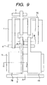
- FIG. 9 is a plane view of a relevant part during the manufacturing process of the semiconductor device of the embodiment 1 of the invention.
- FIG. 10 is a cross section view of a relevant part during the manufacturing process of the semiconductor device following FIG. 8 ;
- FIG. 11 is a cross section view of a relevant part during the manufacturing process of the semiconductor device following FIG. 10 ;
- FIG. 12 is a cross section view of a relevant part during the manufacturing process of the semiconductor device following FIG. 11 ;
- FIG. 13 is a cross section view of a relevant part during the manufacturing process of the semiconductor device following FIG. 12 ;
- FIG. 14 is a cross section view of a relevant part during the manufacturing process of the semiconductor device following FIG. 13 ;
- FIG. 15 is a cross section view of a relevant part during the manufacturing process of the semiconductor device following FIG. 14 ;
- FIG. 16 is a plane view of a relevant part during the manufacturing process of the semiconductor device of the embodiment 1 of the invention.
- FIG. 17 is a cross section view of a relevant part during the manufacturing process of the semiconductor device following FIG. 15 ;
- FIG. 18 is a plane view of a relevant part during the manufacturing process of the semiconductor device following FIG. 16 ;
- FIG. 19 is a cross section view of a relevant part during the manufacturing process of the semiconductor device following FIG. 17 ;
- FIG. 20 is a cross section view of a relevant part during the manufacturing process of the semiconductor device following FIG. 18 ;
- FIG. 21 is a cross section view of a relevant part during the manufacturing process of the semiconductor device of the embodiment 1 of the invention.
- FIG. 22 is a cross section view of a relevant part for explaining a method of manufacturing a semiconductor device of embodiment 2 of the invention.
- FIG. 23 is a cross section view of a relevant part during a manufacturing process of the semiconductor device following FIG. 22 ;
- FIG. 24 is a cross section view of a relevant part during the manufacturing process of the semiconductor device following FIG. 23 ;
- FIG. 25 is a cross section view of a relevant part during the manufacturing process of the semiconductor device following FIG. 24 ;
- FIG. 26 is a cross section view of a relevant part during the manufacturing process of the semiconductor device following FIG. 25 ;
- FIG. 27 is a cross section view of a relevant part during the manufacturing process of the semiconductor device following FIG. 26 ;
- FIG. 28 is a cross section view of a relevant part during the manufacturing process of the semiconductor device following FIG. 27 ;
- FIG. 29 is a cross section view of a relevant part during the manufacturing process of the semiconductor device following FIG. 28 ;
- FIG. 30 is a cross section view of a relevant part during the manufacturing process of the semiconductor device following FIG. 29 ;
- FIG. 31 is a cross section view of a relevant part during the manufacturing process of the semiconductor device following FIG. 30 ;
- FIG. 32 is a plane view of a relevant part for explaining a method of manufacturing a semiconductor device of embodiment 3 of the invention.
- FIG. 33 is a cross section view of a relevant part for explaining the method of manufacturing the semiconductor device of the embodiment 3 of the invention.
- FIG. 34 is a cross section view of a relevant part during a manufacturing process of the semiconductor device following FIG. 33 ;
- FIG. 35 is a cross section view of a relevant part during the manufacturing process of the semiconductor device following FIG. 34 ;
- FIG. 36 is a cross section view of a relevant part during the manufacturing process of the semiconductor device following FIG. 35 ;
- FIG. 37 is a cross section view of a relevant part during the manufacturing process of the semiconductor device following FIG. 36 ;
- FIG. 38 is a cross section view of a relevant part during the manufacturing process of the semiconductor device following FIG. 37 ;
- FIG. 39 is a plane view of a relevant part during the manufacturing process of the semiconductor device of the embodiment 3 of the invention.
- FIG. 40 is a cross section view of a relevant part during the manufacturing process of the semiconductor device following FIG. 38 ;
- FIG. 41 is a cross section view of a relevant part during the manufacturing process of the semiconductor device following FIG. 40 ;
- FIG. 42 is a cross section view of a relevant part during the manufacturing process of the semiconductor device following FIG. 41 ;
- FIG. 43 is a cross section view of a relevant part during the manufacturing process of the semiconductor device following FIG. 42 ;
- FIG. 44 is a cross section view of a relevant part during the manufacturing process of the semiconductor device following FIG. 43 ;
- FIG. 45 is a plane view of a relevant part during the manufacturing process of the semiconductor device following FIG. 44 ;
- FIG. 46 is a cross section view of a relevant part during the manufacturing process of the semiconductor device following FIG. 45 ;
- FIG. 47 is a cross section view of a relevant part during the manufacturing process of the semiconductor device following FIG. 46 ;
- FIG. 48 is a cross section view of a relevant part during the manufacturing process of the semiconductor device following FIG. 47 ;
- FIG. 49 is a plane view of a relevant part during the manufacturing process of the semiconductor device of the embodiment 3 of the invention.
- FIG. 50 is a cross section view of a relevant part during the manufacturing process of the semiconductor device following FIG. 48 ;
- FIG. 51 is a plane view of a relevant part during the manufacturing process of the semiconductor device following FIG. 49 ;
- FIG. 52 is a cross section view of a relevant part during the manufacturing process of the semiconductor device following FIG. 50 ;
- FIG. 53 is a cross section view of a relevant part during the manufacturing process of the semiconductor device of the embodiment 3 of the invention.
- FIG. 54 is a cross section view of a relevant part for explaining a semiconductor device that the inventor investigated.
- FIG. 1 is an equivalent circuit diagram of a memory cell in a nonvolatile memory of a semiconductor device of the embodiment 1, and an area enclosed by a dashed line corresponds to a memory cell.
- floating gates of a plurality of nonvolatile memory elements PM 1 , PM 2 are used as gate electrodes of a plurality of readout MISFETs DM 1 , DM 2 in OR logic connection, and a control gate cg of the nonvolatile memory elements PM 1 and PM 2 is set to be 1.5 V during readout.
- the floating gates of the two nonvolatile memory elements PM 1 , PM 2 are connected in series to the gate electrodes of the readout MISFETs DM 1 and DM 2 respectively.
- the nonvolatile memory elements PM 1 and PM 2 have MIS capacitance elements PM 1 b and PM 2 b in which capacitance electrodes are provided on semiconductor regions working as control gate electrodes (described later in detail) via insulating layers, MISFETs PM 1 a and PM 2 a having sources and drains formed on other semiconductor regions, and gate electrodes, respectively.
- the MIS capacitance elements PM 1 b and PM 2 b are configured by capacitance of MISFET structures in which sources, drains, and back gates are commonly connected respectively.
- the capacitance electrodes of the MIS capacitance elements PM 1 b and PM 2 b are commonly connected to the gate electrodes of the MISFETs PM 1 a , PM 2 a and thus work as the floating gate electrodes, respectively.
- a drain of the readout MISFET DM 2 is coupled to a control node pu via n-channel MISFETs TR 3 and TR 4 , and therefore electric potential of a coupling node rl between the n-channel MISFET TR 3 and the n-channel MISFET TR 4 is provided to a write/read control circuit (omitted to be shown) as output.
- the MISFETs PM 1 a and PM 2 a are coupled to a control node wl via n-channel MISFETs TR 1 and TR 2 .
- Gate electrodes of the n-channel MISFETs TR 1 to TR 4 are biased by power voltage Vdd.
- the source line sl and the control gate cg are set to be 9 V, and the control node wl is set to be 0 V so that the nonvolatile memory elements PM 1 and PM 2 are turned on, and thus hot electron injection is performed from a source line sl side to the floating gates.
- the control node pu is applied with 1.5 V
- the control gate cg is also applied with 1.5 V, so that electrical potential of the coupling node rl, which is determined by a switch state or a mutual conductance state of the readout MISFETs DM 1 , DM 2 corresponding to storage charge on the floating gates, is latched by a latch circuit (omitted to be shown) in a subsequent stage.
- both sides of the source (source line sl) and the drain (control node wl) of the nonvolatile memory elements PM 1 and PM 2 are fixed to 0 V.
- weak hot electrons may not be injected from the MISFETs PM 1 a and PM 2 a into the floating gates during readout.
- weak hot electron injection may by naturally induced from the readout MISFETs DM 1 and DM 2 into the floating gates, since the n-channel MISFETs TR 4 and TR 3 , and the readout MISFETs DM 2 and DM 1 are vertically stacked, drain voltage of the readout MISFETs DM 1 and DM 2 is decreased to voltage of the control node pu or lower.
- a control level of the control gate cg is also low during readout, such hot electron injection can be estimated to be small as to be substantially neglected. Consequently, the readout error rate of the nonvolatile memory elements PM 1 and PM 2 themselves can be reduced.
- the memory cell as shown in FIG. 1 is a unit data cell, and a plurality of the unit data cells are collected, so that an electric program circuit for the nonvolatile memory elements of a plurality of unit data cells is formed, and the plurality of unit data cells become a memory circuit of relief data for a circuit to be relieved.
- reliability of bad cell relief can be improved.
- a fuse program circuit may be further provided as a different relief data memory circuit for the circuit to be relieved, which is for storing relief data depending on a fusing condition of a fuse element.
- Relief for a bad cell detected in a wafer level is performed by a fuse program circuit, and the electric program circuit is used for a bad cell detected after burn-in, thereby relief efficiency can be improved.
- FIG. 2 shows a mat selection relief circuit diagram of DRAM for explaining relief of a bad memory cell of the DRAM by the redundancy.
- a column decoder CLD for write control, write driver WTD, row decoder LWD, and word driver WDD are added to replace a previous laser meltdown fuse with the nonvolatile memory element in the embodiment 1.
- Writing is performed to the nonvolatile memory element, thereby a state equivalent to a state where a fuse is melted can be realized, and readout operation may be the same operation as in the case of the previous laser meltdown fuse.
- Power voltage Vpp necessary for writing is externally supplied.
- Memory cells MC having a basic configuration as described in FIG.
- Writing data lines s 10 to s 14 are connected to the writing driver WTD, and writing word lines w 10 to w 17 (corresponding to the control node w 1 (refer to FIG. 1 )) are connected to the word driver WDD.
- the column decoder CLD decodes a column address signal CADD to generate a selection signal of the writing data lines s 10 to s 14 during writing operation, so that a selected writing data line is driven by the writing driver WTD.
- Selection of the writing word lines w 10 to w 17 during writing operation is directed to the word driver WDD by the row decoder LWD for decoding a low address signal RADD.
- Readout is performed in 8 memory cells MC selected in column by mat selection signals MS 0 to MS 4 .
- Readout data are supplied to an address comparison circuit ACC as relief address data CRA 0 to CRA 7 , and compared with corresponding 8 bits of an access address signal at that time, and comparison results YSEN and YR are used for selection control of redundancy.
- Respective plane views in FIGS. 3 to 20 show a single memory cell.
- a portion marked with a reference A indicates a cross section of a memory cell along a line A-A of a corresponding plane view
- a portion marked with a reference B indicates a cross section of a memory cell along a line B-B of a corresponding plane view
- a portion marked with a reference C indicates a cross section of a memory cell along a line C-C of a corresponding plane view
- other portions indicate cross sections of a part of a peripheral circuit region (first region), respectively.
- element isolation grooves 2 are formed in element isolation regions on a main surface of a semiconductor substrate (hereinafter, simply mentioned as substrate) 1 including, for example, p-type single crystal silicon.
- substrate a semiconductor substrate
- grooves are formed, for example, by performing dry etching the main surface of the substrate 1 , then an insulating film such as a silicon oxide film 3 is deposited on the substrate 1 including the insides of the grooves by a CVD (Chemical Vapor Deposition) process, and then an unnecessary silicon oxide film 3 outside the grooves is polished and removed by a chemical mechanical polishing (CMP) process, thereby silicon oxide films 3 are left within the grooves.
- the element isolation grooves 2 are formed, thereby active regions whose peripheries are defined by the element isolation grooves 2 , are formed on the main surface of the substrate 1 of a memory array.
- a part of the substrate 1 is subjected to ion implantation of an n-type impurity (for example, P (phosphorous)), and a different part of the substrate is subjected to ion implantation of a p-type impurity (for example, B (boron)), then the substrate 1 is subjected to heat treatment to diffuse the impurities into the substrate 1 , thereby a p-type well 4 and an n-type well 5 are formed on the main surface of the substrate 1 .
- an n-type impurity for example, P (phosphorous)
- a p-type impurity for example, B (boron
- the active regions may be defined by forming field insulating films 3 A as shown in FIG. 5 instead of the element isolation grooves 2 .
- Such field insulating films 3 A can be formed by the so-called LOCOS (Local Oxidation of Silicon) process in which a pattern of a silicon nitride film as an oxidation resistance film is formed on surfaces of the substrate 1 , which are to be active regions, and then the surfaces of the substrate 1 are thermally oxidized.
- LOCOS Local Oxidation of Silicon
- the substrate 1 is thermally oxidized to form gate insulating films 6 including, for example, silicon oxide on respective surfaces of the p-type wells 4 and the n-type wells 5 .
- gate insulating films 6 including, for example, silicon oxide on respective surfaces of the p-type wells 4 and the n-type wells 5 .
- a polycrystalline silicon film 7 is formed as a first conductive film on the gate insulating films 6 by, for example, a CVD process, and then an insulating film (second insulating film) 8 including a silicon oxide film or the like is deposited on an upper part of the polycrystalline silicon film 7 by, for example, the CVD process.
- polycrystalline silicon films 7 formed on the p-type wells 4 have been implanted with an impurity showing an n-type conduction type
- polycrystalline silicon films 7 formed on the n-type wells 5 have been implanted with an impurity showing an p-type conduction type, respectively.
- the insulating film 8 in the peripheral circuit region is removed by dry etching using a photoresist film (omitted to be shown), which has been patterned by a photolithography technique, as a mask.
- a photoresist film (omitted to be shown)
- a photolithography technique as a mask.
- an insulating film (fifth insulating film) is deposited on the substrate 1 by, for example, CVD process, the film including a silicon oxide film having a thickness of about 10 nm or more.
- the insulating films 9 and 8 are patterned by dry etching using a photoresist film (omitted to be shown) patterned by the photolithography technique as a mask.
- a photoresist film (omitted to be shown) patterned by the photolithography technique as a mask.
- the polycrystalline silicon film 7 acts as an etching stopper, a cap film including the insulating films 9 and 8 can be formed in the memory cell region (A-A, B-B and C-C), and a cap film including the insulating film 9 can be formed in the peripheral circuit region.
- the gate electrode (first gate electrode) 7 A acts as the floating gate electrode of the MISFET PM 1 a (refer to FIG. 1 ), gate electrode of the readout MISFET DM 1 (refer to FIG. 1 ), and a capacitance electrode of the MIS capacitance element MP 1 b (refer to FIG. 1 ).
- the gate electrode 7 B acts as the floating gate electrode of the MISFET PM 2 a (refer to FIG. 1 ), gate electrode of the readout MISFET DM 2 (refer to FIG.
- the gate electrode 7 C acts as gate electrodes of the n-channel MISFETs TR 1 to TR 4 .
- the gate electrode 7 D (second gate electrode) acts as a gate electrode of MISFET formed in the peripheral circuit region.
- the p-type well 4 and the n-type well 5 are partially subjected to ion implantation of phosphorous or arsenic as an n-type impurity, thereby an n-type semiconductor region 10 in a comparatively low concentration is formed, and the n-type well 5 is subjected to ion implantation of boron as a p-type impurity, thereby a p ⁇ -type semiconductor region 11 in a comparatively low concentration is formed.
- the n ⁇ -type semiconductor region 10 is formed for making respective sources and drains of the MISFETs PM 1 a and PM 2 a , readout MISFETs DM 1 and DM 2 , n-channel MISFETs TR 1 to TR 4 , and n-channel MISFETs formed in the peripheral circuit region, into a LDD (lightly doped drain) structure. Furthermore, the n ⁇ -type semiconductor region 10 is formed for configuring part of the control gate cg of the MIS capacitance elements PM 1 b and PM 2 b . The p ⁇ -type semiconductor region 11 is formed for making sources and drains of p-channel MISFETs formed in the periphery circuit region, into the LDD structure.
- a silicon oxide film is deposited on the substrate 1 by the CVD process, then the silicon oxide film and the insulating film 9 are anisotropically etched, thereby sidewall spacers (first insulating film) 12 are formed on sidewalls of the gate electrodes 7 A, 7 B, 7 C and 7 D and the insulating films B.
- the insulating film 9 as the cap film is removed and surfaces of the gate electrodes 7 D are exposed in the peripheral circuit region, however, in the memory cell region (A-A, B-B and C-C), the insulating films 9 and 8 as the cap film are etched in a degree that the insulating film 9 is merely removed by etching, and formed into a structure where the insulating films 8 are left on the gate electrodes A and B.
- the insulating film 9 is somewhat left on the insulating film 8 , it may not cause any problem in MISFET properties.
- the insulating film 8 (or insulating films 9 and 8 ) as the cap film is left on the gate electrodes A and B in the memory cell region, and the insulating film 9 as the cap film on the gate electrode 7 C of the n-channel MISFETs TR 1 to TR 4 and the gate electrode 7 D in the peripheral circuit region is removed.
- the p-type well 4 and the n-type well 5 are partially subjected to ion implantation of phosphorous or arsenic as an n-type impurity, thereby an n + -type semiconductor region 14 in a comparatively high concentration is formed, and the n-type well 5 is subjected to ion implantation of boron as a p-type impurity, thereby a p + -type semiconductor region 15 in a comparatively high concentration is formed.
- the n + -type semiconductor region 14 configures respective sources and drains of the MISFETs PM 1 a and PM 2 a , readout MISFETs DM 1 and DM 2 , n-channel MISFETs TR 1 to TR 4 , and n-channel MISFETs formed in the peripheral circuit region. Furthermore, the n + -type semiconductor region 14 is formed for configuring the control gate cg of the MIS capacitance elements PM 1 b and PM 2 b .
- the p + -type semiconductor region 15 configures a source and a drain of the p-channel MISFET formed in the peripheral circuit region.
- An n + -type semiconductor region 14 formed in the n-type well 5 of the memory cell acts as the control gate cg (refer to FIG. 1 ).
- a silicide layer 18 is formed.
- a Co (cobalt) film is deposited on the substrate 1 by a sputtering process. Then, the substrate 1 is subjected to heat treating to induce a silicide reaction at an interface between the Co film and the gate electrode 7 D in the peripheral circuit region, and an interface between the Co film and the substrate 1 , then an unreacted Co film is removed by etching.
- a silicide (CoSi 2 ) layer 18 is formed on the surface of the gate electrode 7 D and surfaces of the sources and drains (n + -type semiconductor regions 14 and p + -type semiconductor regions 15 ).
- the silicide layers 18 are formed also on the surfaces of the gate electrode 7 C. Moreover, in the memory cell region, the silicide layer 18 is formed also on the surface of the n + -type semiconductor regions 14 . Here, since the insulating film 8 as the cap film is left on the gate electrodes 7 A, 7 B, the silicide layer 18 is not formed. While Co (cobalt) was exemplified as a material of the silicide layer 18 in the embodiment 1, the material is not limited to this, and Ti (titanium), W (tungsten), Ni (nickel) or the like can be also used.
- the MIS capacitance element PM 1 a is a capacitance element using the substrate 1 (n-type well 5 ) and the gate electrode 7 A on the n-type well 5 as capacitance electrodes, and using the gate insulating film 6 as a capacitance insulating film.
- the MIS capacitance element PM 2 b is a capacitance element using the substrate 1 (n-type well 5 ) and the gate electrode 7 B on the n-type well 5 as capacitance electrodes, and using the gate insulating film 6 as a capacitance insulating film.
- a silicon nitride film (third insulating film) 19 is deposited on the substrate 1 by the plasma enhanced CVD process in a way of covering the gate electrodes 7 A, 7 B, 7 C and 7 D, insulating films 9 and 8 , and sidewall spacer 12 .
- the silicon nitride film 19 works such that when an interlayer insulating film is formed on the substrate 1 in a subsequent step, and contact holes are formed in the interlayer insulating film, the holes being penetrated to each of the n + -type semiconductor region 14 and the p + -type semiconductor region 15 , the contact holes are prevented from being penetrated to the gate electrodes 7 A, 7 B, 7 C and 7 D by increasing etching selectivity ratio to the sidewall spacers formed from the silicon oxide film.
- the silicon nitride film 19 works to prevent a surface of the silicide layer from being reduced by overetching. That is, the silicon nitride film 19 works as an etching stopper film.
- the plasma enhanced CVD process is preferably used, by which a film can be formed at low temperature compared with the thermal CVD process as described before.
- NH 3 gas when used as deposition gas, it may apprehensively affect on the characteristics of the device. Therefore, an approach of plasma decomposition of a mixture of SiH 4 (silane) and N 2 (nitrogen) can be exemplified.
- SiH 4 +N 2 ⁇ Si x N y +zH 2 is given (x, y, or z is an integer).
- the silicon nitride film 19 is formed by the approach, a silicon-rich film is easily formed in an initial stage of film formation.
- a silicon nitride film 19 is in a condition of being electrically connected to gate electrodes 7 A and 7 B of the MISFETs PM 1 a and PM 2 a forming the nonvolatile memory elements PM 1 and PM 2
- since electric charges tend to leak in a portion of the silicon-rich film electric charges stored in the gate electrodes 7 A and 7 B as the floating gate electrodes of the nonvolatile memory elements PM 1 and PM 2 may leak from interfaces between the silicon nitride film 19 and the gate electrodes 7 A, 7 B, and the electric charges may reach the n + -type semiconductor region 14 , and thus discharged from a plug (formed in a subsequent step) electrically connected to the n + -type semiconductor region 14 . That is, the data holding property of the nonvolatile memory may be apprehensively reduced.
- the sidewall spacer 12 or the insulating film 8 which is formed from a silicon oxide film that hardly allows leakage of electric charges compared with the silicon nitride film 19 (highly insulative compared with the silicon nitride film 19 ), is formed between the silicon nitride film 19 and the gate electrodes 7 A, 7 B. That is, the silicon nitride film 19 as an etching stopper film is formed on the gate electrodes 7 A, 7 B via the insulating film 8 or the sidewall spacer 12 which is a silicon oxide film highly insulative compared with the silicon nitride film 19 . Therefore, since the electric charges stored in the gate electrodes 7 A, 7 B are hardly allowed to leak, reduction in the data holding property of the nonvolatile memory of the embodiment 1 can be prevented. That is, reliability of the semiconductor device can be improved.
- a silicon oxide film 20 is deposited by, for example, the CVD process, and then a surface of the silicon oxide film 20 is planarized by a chemical mechanical polishing process.
- the silicon oxide film 20 is subjected to dry etching using a photoresist film as a mask, thereby contact holes 21 are formed, which are penetrated to each of the n + -type semiconductor region 14 and the p + -type semiconductor region 15 .
- the silicon nitride film 19 acts as an etching stopper film in etching the silicon oxide film 20 .
- plugs 22 are formed within the contact holes 21 .
- a Ti (titanium) film and a TiN (titanium nitride) film is deposited on the silicon oxide film 20 including the insides of the contact holes 21 by a sputtering process, then a TiN film and a W (tungsten) film as a metal film are deposited by the CVD process, and then the W film, TiN film and Ti film outside the contact holes 21 are removed by the chemical mechanical polishing process.
- a plurality of wiring lines 23 are formed on the silicon oxide film 20 and the plugs 22 .
- a Ti film, an Al (aluminum) alloy film and a TiN film are sequentially deposited on the silicon oxide film 20 by the sputtering process, and then the Ti film, Al (aluminum) alloy film and TiN film are patterned by dry etching using a photoresist film as a mask.
- the wiring lines 23 include a wiring line to be electrically connected to the control gate cg (refer to FIG. 1 ), and a wiring line to be the source line sl (refer to FIG. 1 ).
- a silicon oxide film (omitted to be shown) is deposited on the substrate 1 as an interlayer insulating film, then contact holes penetrated to the wiring lines 23 are formed in the silicon oxide film, and then plugs 25 similar to the plugs 22 are formed in the contact holes.
- a plurality of wiring lines 26 are formed on the silicon oxide film and the plugs, so that the semiconductor device of the embodiment is manufactured.
- the wiring lines 26 can be formed in the same steps as in the wiring lines 23 .
- the wiring lines 26 include a wiring line electrically connected to the coupling node rl (refer to FIG. 1 ), a wiring line electrically connected to the power voltage Vdd (refer to FIG.
- the gate electrodes 7 A, 7 B, 7 C and 7 D were formed from the polycrystalline silicon film 7 was described in the embodiment 1, as shown in FIG. 21 , the gate electrodes 7 A, 7 B, 7 C and 7 D may be formed from a stacked film of the polycrystalline silicon film 7 and a WSi (tungsten silicide) film 7 F, and again in that case, similar effects can be obtained.
- the silicide layer 18 (for example, refer to FIG. 13 ) may be omitted.
- a structure of a nonvolatile memory of embodiment 2 is described together with a manufacturing process of the memory using FIGS. 22 to 31 . Since a planar structure of a memory cell of the nonvolatile memory of the embodiment 2 is approximately the same as a plane structure of the memory cell shown in the embodiment, the planar structure is omitted to be shown in the embodiment 2.
- a portion marked with a reference B shows a cross section of the memory cell along the line B-B in each of plane views used in the embodiment 1
- a portion marked with a reference C shows a cross section of the memory cell along the line C-C in each of corresponding plane views used in the embodiment 1
- other portions show cross sections of part of the peripheral circuit region.
- an n-channel MISFET and a p-channel MISFET which configure a peripheral circuit, and a resistance element are formed. That is, in description with FIG. 22 as an example, a cross section view of a memory cell along a line B-B of each plane view, a cross section view of a memory cell along a line C-C of each plane view, the peripheral circuit region in which the n-channel MISFET and the p-channel MISFET are formed, and a resistance element formation region are shown from the left in FIG. 22 .
- a manufacturing process of the nonvolatile memory of the embodiment 2 has the same steps as steps described using FIGS. 3 to 6 in the embodiment 1 (refer to FIG. 22 ).
- an insulating film (sixth insulating film) 8 is patterned by dry etching using a photoresist film (omitted to be shown) patterned by a photolithography technique as a mask.
- a polycrystalline silicon film 7 is patterned using the patterned insulating film 8 as a mask, so that gate electrodes 7 A (refer to FIG. 9 and FIG. 10 ), 7 B and 7 C (refer to FIG. 10 ), and 7 D, and a resistance element 7 R are formed.
- the resistance element 7 R is formed on the silicon oxide film 3 .
- the resistance element 7 R is formed in a step of forming the gate electrodes 7 A, 7 B, and the gate electrode 7 C of the n-channel MISFETs TR 1 to TR 4 in the memory cell region, and the gate electrode 7 D in the peripheral circuit region.
- the manufacturing process can be simplified, and increase in the number of masks can be prevented.
- a p-type well 4 is subjected to ion implantation of phosphorous or arsenic as an n-type impurity, thereby an n + -type semiconductor region 10 in a comparatively low concentration is formed, and an n-type well 5 is subjected to ion implantation of boron as a p-type impurity, thereby a p ⁇ -type semiconductor region 11 in a comparatively low concentration is formed.
- a silicon oxide film is deposited on a substrate 1 by the CVD process, then the silicon oxide film is anisotropically etched, thereby sidewall spacers 12 are formed on sidewalls of the gate electrodes 7 A, 7 B, 7 C and 7 D and the resistance element 7 R.
- the insulating film 8 formed on the gate electrodes 7 A, 7 B, 7 C and 7 D, and on the resistance element 7 R is removed.
- the p-type well 4 is subjected to ion implantation of phosphorous or arsenic as an n-type impurity, thereby an n + -type semiconductor region 14 in a comparatively high concentration is formed, and the n-type well 5 is subjected to ion implantation of boron as a p-type impurity, thereby a p + -type semiconductor region 15 in a comparatively high concentration is formed.
- the n + -type semiconductor region 14 configures respective sources and drains of the MISFETs PM 1 a (refer to FIG. 1 ) and PM 2 a (refer to FIG. 1 ), readout MISFETs DM 1 (refer to FIG.
- n + -type semiconductor region 14 is formed for configuring the control gate cg of the MIS capacitance elements PM 1 b and PM 2 b .
- the p + -type semiconductor region 15 configures sources and drains of the p-channel MISFETs formed in the peripheral circuit region.
- a silicon oxide film (second insulating film) 9 A about 10 nm or more in thickness is deposited on the substrate 1 by the CVD process.
- the insulating film 9 A is patterned by dry etching using a photoresist film (omitted to be shown) patterned by a photolithography technique as a mask.
- the insulating film 9 A is left on tops and sides of the gate electrodes 7 A, 7 B and 7 C (refer to FIG. 10 ) and the resistance element 7 R.
- An opening 9 B penetrated to the resistance element 7 R is formed in the insulating film 9 A on the resistance element 7 R.
- the opening 9 B is provided for forming a silicide layer 18 formed on a surface of the resistance element 7 R in a subsequent step. That is, in the embodiment 2, in a step of forming the insulating film 9 A formed for providing the opening 9 B on the resistance element 7 R, the insulating film 9 A is formed on the gate electrodes 7 A and 7 B in the memory cell region.
- the manufacturing process can be simplified, and increase in the number of masks can be prevented.
- a silicide layer 18 is formed.
- a method of forming the silicide layer 18 is the same as that in the embodiment 1: first, for example, a Co film is deposited on the substrate 1 by the sputtering process. Then, the substrate 1 is subjected to heat treating to induce a silicide reaction at an interface between the Co film and the gate electrode 7 D in the peripheral circuit region, an interface between the Co film and the resistance element 7 R on a bottom of the opening 9 B, and an interface between the Co film and the substrate 1 , then an unreacted Co film is removed by etching.
- the silicide layer 18 as a silicide layer is formed on the surface of the gate electrode 7 D, a surface of the resistance element 7 R on the bottom of the opening 9 B and surfaces of the sources and drains (n + -type semiconductor regions 14 and p + -type semiconductor regions 15 ).
- the MISFETs PM 1 a (refer to FIG. 1 ), PM 2 a (refer to FIG. 1 ) and the MIS capacitance elements PM 1 b (refer to FIG. 1 ), PM 2 b (refer to FIG. 1 ), which form nonvolatile memory elements PM 1 (refer to FIG. 1 ), PM 2 (refer to FIG. 1 ), readout MISFETs DM 1 (refer to FIG.
- DM 2 (refer to FIG. 1 ), and n-channel MISFETs TR 1 to TR 4 (refer to FIG. 1 ) are formed in the memory cell, and a p-channel MISFET Qp and an n-channel MISFET Qn are formed in the peripheral circuit region.
- a silicon nitride film 19 is deposited on the substrate 1 by the plasma enhanced CVD process.
- the silicon nitride film 19 is formed by using a mixture of SiH 4 and N 2 as deposition gas, and performing plasma decomposition of the deposition gas.
- the sidewall spacer 12 and the insulating film 9 A are disposed in a stacked condition between the silicon nitride film 19 and the gate electrodes 7 A, 7 B. Therefore, since the electric charges stored in the gate electrodes 7 A, 7 B are hardly allowed to leak, reduction in the data holding property of the nonvolatile memory of the embodiment 2 can be prevented further securely. That is, reliability of the semiconductor device can be improved.
- a silicon oxide film 20 is deposited on the substrate 1 by, for example, the CVD process, then a surface of the silicon oxide film 20 is planarized by the chemical mechanical polishing process. Then, as shown in FIG. 31 , the silicon oxide film 20 is subjected to dry etching using a photoresist film as a mask, thereby contact holes 21 are formed, which are penetrated to each of the n + -type semiconductor region 14 , the p + -type semiconductor region 15 , and the resistance element 7 R. At that time, the silicon nitride film 19 works as an etching stopper film in etching the silicon oxide film 20 .
- plugs 22 similar to the plugs 22 as shown in the embodiment 1 are formed within the contact holes 21 .
- a plurality of wiring lines 23 similar to the wiring lines 23 as shown in the embodiment 1 are formed on the silicon oxide film 20 and the plugs 22 .
- a semiconductor device of the embodiment 2 is manufactured through the same steps as steps described using FIG. 20 in the embodiment 1.
- the resistance element can be concurrently formed in the step of forming the gate electrodes of the MISFETs in the memory cell region and the peripheral circuit region.
- the insulating film 9 A can be formed on the gate electrodes 7 A and 7 B in the memory cell region in the step of forming the insulating film 9 A formed for providing the openings 9 B on the resistance element 7 R.
- FIGS. 32 to 52 a structure of a nonvolatile memory of embodiment 3 is described together with a manufacturing process of the memory using FIGS. 32 to 52 .
- a portion marked with a reference A shows a cross section of a memory cell along a line A-A in a corresponding plane view
- a portion marked with a reference B shows a cross section of a memory cell along a line B-B in a corresponding plane view
- other portions show cross sections of part of the peripheral circuit region.
- an n-channel MISFET configuring a peripheral circuit, a capacitance element, and a resistance element are formed.
- a conduction type is merely inverted and a structure is approximately the same with respect to the n-channel MISFET, therefore a region where the p-channel MISFET is formed is omitted to be shown in each cross section view in the embodiment 3.
- element isolation grooves 2 , p-type wells 4 , and n-type wells 5 are formed according to the same steps as steps described using FIG. 3 and FIG. 4 in the embodiment 1 (refer to FIG. 32 and FIG. 33 ).
- the substrate 1 is thermally oxidized so that gate insulating films 6 including, for example, silicon oxide are formed on respective surfaces of the p-type wells 4 and the n-type wells 5 .
- gate insulating films 6 including, for example, silicon oxide are formed on respective surfaces of the p-type wells 4 and the n-type wells 5 .
- polycrystalline silicon films 7 are formed as conductive films on the gate insulating films 6 by, for example, the CVD process.
- insulating films (fourth insulating films) ONO are formed on the polycrystalline silicon films 7 .
- the insulating film ONO is formed by sequentially depositing a silicon oxide film about 5 nm in thickness, silicon nitride film about 20 nm in thickness, and silicon oxide film about 5 nm in thickness from a lower layer.
- the insulating films ONO and the polycrystalline silicon films 7 are patterned by etching using a photoresist film as a mask.
- the insulating films ONO and the polycrystalline silicon films 7 are left in regions where the capacitance elements are formed in the memory cell region and the peripheral circuit region, and removed in other regions.
- the polycrystalline silicon film 7 left in the region where the capacitance element is formed in the peripheral circuit region acts as a lower electrode (first capacitance electrode) KD of the capacitance element.
- a polycrystalline silicon film (second conductive film) 7 S is deposited on the substrate 1 by, for example, the CVD process.
- an insulating film 8 is deposited on the polycrystalline silicon film 7 S by, for example, the CVD process.
- an insulating film 8 to be a cap film is patterned by etching using a photoresist film as a mask.
- the polycrystalline silicon film 7 S is patterned by dry etching using the cap film 8 as a mask.
- the insulating film ONO acts as an etching stopper.
- the insulating film 8 and the polycrystalline silicon film 7 S are left in a region where the gate electrodes are formed in a subsequent step, and left on element isolation grooves 2 (silicon oxide films 3 ).
- the polycrystalline silicon films 7 S left in the memory cell region act as control gates (third electrodes) of nonvolatile memory elements PM 1 , PM 2 (refer to FIG. 1 ).
- a gate electrode 7 D including the polycrystalline silicon film 7 S, a resistance element 7 R, and an upper electrode (second capacitance electrode) JD of the capacitance element are formed, consequently a capacitance element CAPA with the lower electrode KD and the upper electrode JD as capacitance electrodes, and with the insulating film ONO as a capacitance insulating film.
- the peripheral circuit region is covered by a photoresist film RESI, and the insulating film ONO and the polycrystalline silicon film 7 are subjected to etching using the photoresist film RESI and the insulating film 8 as a mask.
- gate electrodes 7 A, 7 B and 7 C including the polycrystalline silicon film 7 , insulating film ONO, and polycrystalline silicon film 7 S are formed.
- the polycrystalline silicon films 7 S in the memory cell region configure control gate electrodes of the nonvolatile memory elements PM 1 and PM 2
- the polycrystalline silicon film 7 configure floating gate electrodes of the nonvolatile memory elements PM 1 and PM 2 .
- the p-type well 4 and the n-type well 5 are partially subjected to ion implantation of phosphorous or arsenic as an n-type impurity, thereby an n ⁇ -type semiconductor region 10 in a comparatively low concentration is formed.
- the memory cell region, and a region where the resistance element 7 R and the capacitance element CAPA are formed in the peripheral circuit region are covered by a photoresist film RESI 2 .
- the p-type well 4 in the peripheral circuit region is subjected to ion implantation of phosphorous or arsenic as an n-type impurity, thereby an n ⁇ -type semiconductor region 10 A in a comparatively low concentration is formed, and the n-type well is subjected to ion implantation of boron as an p-type impurity, thereby a p ⁇ -type semiconductor region in a comparatively low concentration is formed.
- a silicon oxide film is deposited on the substrate 1 by the CVD process, then the silicon oxide film and the insulating film 8 are anisotropically etched, thereby sidewall spacers 12 are formed on sidewalls of the gate electrodes 7 A, 7 B, 7 C and 7 D, resistance element 7 R, and capacitance element CAPA.
- the sidewall spacers 12 are formed also on sidewalls of the polycrystalline silicon patterns left on the element isolation grooves 2 , and dummy patterns DP are formed from the polycrystalline silicon patterns and the sidewall spacers 12 on the element isolation grooves 2 .
- the dummy patterns DP work as a mask so that the silicon oxide films 3 in the element isolation grooves 2 are not etched when the silicon oxide film on the substrate 1 is subjected to etching in a subsequent step.
- an insulating film 9 C is formed by depositing a silicon oxide film about 20 nm to 30 nm in thickness on the substrate 1 by the CVD process.
- the p-type well 4 and the n-type well 5 are partially subjected to ion implantation of phosphorous or arsenic as an n-type impurity, thereby an n + -type semiconductor region 14 in a comparatively high concentration is formed, and the n-type well 5 is subjected to ion implantation of boron as a p-type impurity, thereby a p + -type semiconductor region 15 in a comparatively high concentration is formed.
- the n + -type semiconductor region 14 configures respective sources and drains of the MISFETs PM 1 a (refer to FIG. 1 ) and PM 2 a (refer to FIG. 1 ), readout MISFETs DM 1 (refer to FIG. 1 ) and DM 2 (refer to FIG. 1 ), n-channel MISFETs TR 1 to TR 4 (refer to FIG. 1 ), and n-channel MISFETs formed in the peripheral circuit region.
- the p + -type semiconductor region 15 configures a source and a drain of the p-channel MISFET formed in the peripheral circuit region.
- the insulating film 9 C is patterned by dry etching using a photoresist film (omitted to be shown) patterned by the photolithography technique as a mask.
- the insulating film 9 C is left on the resistance element 7 R.
- An opening 9 B penetrated to the resistance element 7 R is formed in the insulating film 9 C on the resistance element 7 R.
- a Co film is deposited on the substrate 1 by the sputtering process. Then, the substrate 1 is subjected to heat treating to induce a silicide reaction at an interface between the Co film, and the polycrystalline silicon film 7 S and the gate electrode 7 D, an interface between the Co film and the resistance element 7 R on a bottom of the opening 9 B, an interface between a polycrystalline silicon film 7 as a lower electrode of the capacitance element CAPA and the Co film, and an interface between the Co film and the substrate 1 , then an unreacted Co film is removed by etching.
- a silicide layer 18 is formed on surfaces of the polycrystalline silicon film 7 S and the gate electrode 7 D, a surface of the resistance element 7 R on the bottom of the opening 9 B, part of a surface of the lower electrode of the capacitance element CAPA, and surfaces of the sources and drains (n + -type semiconductor region 14 and p + -type semiconductor region 15 ).
- n-channel MISFETs TR 1 to TR 4 are formed in the memory cell, and a p-channel MISFET and an n-channel MISFET Qn are formed in the peripheral circuit region.
- a silicon nitride film 19 is deposited on the substrate 1 by the plasma enhanced CVD process.
- the silicon nitride film 19 is formed by using a mixture of SiH 4 and N 2 as deposition gas, and performing plasma decomposition of the mixture.
- a silicon oxide film 20 is deposited on the substrate 1 by, for example, the CVD process, then a surface of the silicon oxide film 20 is planarized by the chemical mechanical polishing process. Then, as shown in FIG. 49 and FIG. 50 , the silicon oxide film 20 is subjected to dry etching using a photoresist film as a mask, thereby contact holes 21 are formed, which are penetrated to each of the n + -type semiconductor region 14 , the p + -type semiconductor region 15 , the resistance element 7 R, and the resistance element CAPA (upper electrode and lower electrode). Then, plugs 22 similar to the plugs 22 as shown in the embodiment (refer to FIG. 16 and FIG. 17 ) are formed within the contact holes 21 .
- a plurality of wiring lines 23 similar to the wiring lines 23 as shown in the embodiment 1 are formed on the silicon oxide film 20 and the plugs 22 .
- a semiconductor device of the embodiment 3 is manufactured through the same steps as steps described using FIG. 20 in the embodiment 1.
- the resistance element and the capacitance element can be concurrently formed in the step of forming the MISFETs.
- the silicon oxide film which is a film that hardly allows leakage of electric charges (highly insulative film) compared with the silicon nitride film 19 , between the floating gate (polysilicon silicon film 7 ) and the silicon nitride film 19 in the memory cell region, reduction in data holding property of the nonvolatile memory as shown in the embodiment 1 can be prevented.
- the gate electrodes 7 A, 7 B, 7 C and 7 D including the polycrystalline silicon film 7 S, and lower electrodes of the resistance element 7 R and the capacitance element CAPA was described in the embodiment 3, they may be formed by stacking WSi films 7 F on the polycrystalline silicon films 7 S as shown in FIG. 53 .
- the silicide layers 18 (for example, refer to FIG. 13 ) may be omitted.
- a circuit to be relieved is a bad memory cell of DRAM
- the circuit may be a memory cell of microcomputer-equipped DRAM, or a memory cell of microcomputer-equipped SRAM.
- a circuit of relieving an LCD driver can be configured.
- the semiconductor device and the method of manufacturing the device of the invention can be used, for example, for a semiconductor device having a nonvolatile memory and a method of manufacturing the device.
Abstract
Description
Claims (15)
Priority Applications (1)
| Application Number | Priority Date | Filing Date | Title |
|---|---|---|---|
| US12/330,637 US7678649B2 (en) | 2004-04-14 | 2008-12-09 | Semiconductor device and manufacturing method thereof |
Applications Claiming Priority (5)
| Application Number | Priority Date | Filing Date | Title |
|---|---|---|---|
| JP2004-119415 | 2004-04-14 | ||
| JP2004119415 | 2004-04-14 | ||
| US10/592,169 US7612402B2 (en) | 2004-04-14 | 2005-03-17 | Nonvolatile memory semiconductor device and manufacturing method thereof |
| PCT/JP2005/004750 WO2005101519A1 (en) | 2004-04-14 | 2005-03-17 | Semiconductor device and manufacturing method thereof |
| US12/330,637 US7678649B2 (en) | 2004-04-14 | 2008-12-09 | Semiconductor device and manufacturing method thereof |
Related Parent Applications (3)
| Application Number | Title | Priority Date | Filing Date |
|---|---|---|---|
| US10/592,169 Division US7612402B2 (en) | 2004-04-14 | 2005-03-17 | Nonvolatile memory semiconductor device and manufacturing method thereof |
| PCT/JP2005/004750 Division WO2005101519A1 (en) | 2004-04-14 | 2005-03-17 | Semiconductor device and manufacturing method thereof |
| US11/592,169 Division US20070094871A1 (en) | 2005-11-03 | 2006-11-03 | Method for manufacturing a printed circuit board with a film capacitor embedded therein, and a printed circuit board obtained thereby |
Publications (2)
| Publication Number | Publication Date |
|---|---|
| US20090093096A1 US20090093096A1 (en) | 2009-04-09 |
| US7678649B2 true US7678649B2 (en) | 2010-03-16 |
Family
ID=35150262
Family Applications (2)
| Application Number | Title | Priority Date | Filing Date |
|---|---|---|---|
| US10/592,169 Active 2026-02-08 US7612402B2 (en) | 2004-04-14 | 2005-03-17 | Nonvolatile memory semiconductor device and manufacturing method thereof |
| US12/330,637 Expired - Fee Related US7678649B2 (en) | 2004-04-14 | 2008-12-09 | Semiconductor device and manufacturing method thereof |
Family Applications Before (1)
| Application Number | Title | Priority Date | Filing Date |
|---|---|---|---|
| US10/592,169 Active 2026-02-08 US7612402B2 (en) | 2004-04-14 | 2005-03-17 | Nonvolatile memory semiconductor device and manufacturing method thereof |
Country Status (6)
| Country | Link |
|---|---|
| US (2) | US7612402B2 (en) |
| JP (2) | JP4977461B2 (en) |
| KR (1) | KR101144380B1 (en) |
| CN (1) | CN1943037B (en) |
| TW (2) | TW200541082A (en) |
| WO (1) | WO2005101519A1 (en) |
Cited By (2)
| Publication number | Priority date | Publication date | Assignee | Title |
|---|---|---|---|---|
| US20100038693A1 (en) * | 2006-06-22 | 2010-02-18 | Renesas Technology Corp. | Semiconductor device |
| US20110224254A1 (en) * | 2010-03-10 | 2011-09-15 | Probiodrug Ag | Novel inhibitors |
Families Citing this family (11)
| Publication number | Priority date | Publication date | Assignee | Title |
|---|---|---|---|---|
| TW200541082A (en) * | 2004-04-14 | 2005-12-16 | Renesas Tech Corp | Semiconductor device and manufacturing method thereof |
| JP2009016462A (en) * | 2007-07-03 | 2009-01-22 | Renesas Technology Corp | Semiconductor device and its manufacturing method |
| US20090065841A1 (en) * | 2007-09-06 | 2009-03-12 | Assaf Shappir | SILICON OXY-NITRIDE (SiON) LINER, SUCH AS OPTIONALLY FOR NON-VOLATILE MEMORY CELLS |
| WO2010032594A1 (en) * | 2008-09-19 | 2010-03-25 | Semiconductor Energy Laboratory Co., Ltd. | Semiconductor device |
| JP2012164869A (en) * | 2011-02-08 | 2012-08-30 | Renesas Electronics Corp | Semiconductor device and manufacturing method of the same |
| JP5847537B2 (en) * | 2011-10-28 | 2016-01-27 | ルネサスエレクトロニクス株式会社 | Semiconductor device manufacturing method and semiconductor device |
| JP6026914B2 (en) * | 2013-02-12 | 2016-11-16 | ルネサスエレクトロニクス株式会社 | Manufacturing method of semiconductor device |
| CN108666312B (en) * | 2017-03-30 | 2021-05-04 | 联华电子股份有限公司 | Dynamic random access memory element with embedded flash memory and manufacturing method thereof |
| US10756113B2 (en) | 2017-11-23 | 2020-08-25 | Yangtze Memory Technologies Co., Ltd. | Protective structure and fabrication methods for the peripheral circuits of a three-dimensional memory |
| CN107968090B (en) * | 2017-11-23 | 2019-02-12 | 长江存储科技有限责任公司 | The method and structure for preventing peripheral circuit impaired |
| CN107946312B (en) * | 2017-11-23 | 2019-01-29 | 长江存储科技有限责任公司 | The method and structure for preventing peripheral circuit impaired |
Citations (10)
| Publication number | Priority date | Publication date | Assignee | Title |
|---|---|---|---|---|
| JPH04212471A (en) | 1990-07-12 | 1992-08-04 | Hitachi Ltd | Semiconductor integrated circuit device |
| JPH07235613A (en) | 1993-12-28 | 1995-09-05 | Nippon Steel Corp | Semiconductor memory storage and manufacture thereof |
| US5612238A (en) | 1993-12-28 | 1997-03-18 | Nippon Steel Corporation | Method of manufacturing first and second memory cell arrays with a capacitor and a nonvolatile memory cell |
| JPH09289249A (en) | 1996-04-22 | 1997-11-04 | Sony Corp | Fabrication method of semiconductor device |
| JPH1187664A (en) | 1997-04-28 | 1999-03-30 | Nippon Steel Corp | Semiconductor device and its production |
| JP2001196327A (en) | 2000-01-06 | 2001-07-19 | Matsushita Electric Ind Co Ltd | Semiconductor device and method of manufacturing the same |
| JP2001332640A (en) | 2000-05-25 | 2001-11-30 | Nec Corp | Semiconductor memory device and its manufacturing method |
| US20040014323A1 (en) | 2002-07-19 | 2004-01-22 | Mitsubishi Denki Kabushiki Kaisha | Method of fabricating semiconductor device |
| JP2004079893A (en) | 2002-08-21 | 2004-03-11 | Denso Corp | Semiconductor device and method for manufacturing same |
| US20050173753A1 (en) * | 2004-02-06 | 2005-08-11 | Kim Sang-Soo | Semiconductor device and method of fabricating the same |
Family Cites Families (8)
| Publication number | Priority date | Publication date | Assignee | Title |
|---|---|---|---|---|
| JP3507761B2 (en) * | 1990-07-12 | 2004-03-15 | 株式会社ルネサステクノロジ | Semiconductor integrated circuit device |
| KR920006991A (en) * | 1990-09-25 | 1992-04-28 | 김광호 | High Voltage Generation Circuit of Semiconductor Memory Device |
| JP3231470B2 (en) * | 1993-03-31 | 2001-11-19 | 株式会社リコー | Semiconductor device |
| US5940735A (en) * | 1997-08-25 | 1999-08-17 | Advanced Micro Devices, Inc. | Reduction of charge loss in nonvolatile memory cells by phosphorus implantation into PECVD nitride/oxynitride films |
| KR19990021388A (en) * | 1997-08-30 | 1999-03-25 | 김영환 | Capacitor Manufacturing Method of Analog Semiconductor Device |
| US6555865B2 (en) * | 2001-07-10 | 2003-04-29 | Samsung Electronics Co. Ltd. | Nonvolatile semiconductor memory device with a multi-layer sidewall spacer structure and method for manufacturing the same |
| JP2003249579A (en) * | 2003-02-10 | 2003-09-05 | Toshiba Corp | Non-volatile semiconductor memory device and method of manufacturing the same |
| TW200541082A (en) * | 2004-04-14 | 2005-12-16 | Renesas Tech Corp | Semiconductor device and manufacturing method thereof |
-
2005
- 2005-02-24 TW TW094105628A patent/TW200541082A/en unknown
- 2005-02-24 TW TW097105471A patent/TW200826300A/en unknown
- 2005-03-17 WO PCT/JP2005/004750 patent/WO2005101519A1/en active Application Filing
- 2005-03-17 US US10/592,169 patent/US7612402B2/en active Active
- 2005-03-17 CN CN2005800112877A patent/CN1943037B/en active Active
- 2005-03-17 KR KR1020067021314A patent/KR101144380B1/en active IP Right Grant
- 2005-03-17 JP JP2006512285A patent/JP4977461B2/en active Active
-
2008
- 2008-12-09 US US12/330,637 patent/US7678649B2/en not_active Expired - Fee Related
-
2011
- 2011-02-02 JP JP2011020290A patent/JP5342573B2/en active Active
Patent Citations (17)
| Publication number | Priority date | Publication date | Assignee | Title |
|---|---|---|---|---|
| US6501689B2 (en) | 1990-07-12 | 2002-12-31 | Hitachi, Ltd. | Semiconductor integrated circuit device |
| US5457335A (en) | 1990-07-12 | 1995-10-10 | Hitachi, Ltd. | Floating gate FET with hydrogen barrier shield |
| JPH04212471A (en) | 1990-07-12 | 1992-08-04 | Hitachi Ltd | Semiconductor integrated circuit device |
| JPH07235613A (en) | 1993-12-28 | 1995-09-05 | Nippon Steel Corp | Semiconductor memory storage and manufacture thereof |
| US5612238A (en) | 1993-12-28 | 1997-03-18 | Nippon Steel Corporation | Method of manufacturing first and second memory cell arrays with a capacitor and a nonvolatile memory cell |
| JPH09289249A (en) | 1996-04-22 | 1997-11-04 | Sony Corp | Fabrication method of semiconductor device |
| JPH1187664A (en) | 1997-04-28 | 1999-03-30 | Nippon Steel Corp | Semiconductor device and its production |
| US20030047747A1 (en) | 1997-04-28 | 2003-03-13 | Yoshihiro Kumazaki | Non-volatile semiconductor memory with single layer gate structure |
| US6489650B2 (en) | 1997-04-28 | 2002-12-03 | Nippon Steel Corporation | Semiconductor device and a method of manufacturing the same |
| JP2001196327A (en) | 2000-01-06 | 2001-07-19 | Matsushita Electric Ind Co Ltd | Semiconductor device and method of manufacturing the same |
| US20010048130A1 (en) | 2000-05-25 | 2001-12-06 | Nec Corporation | Semiconductor device |
| JP2001332640A (en) | 2000-05-25 | 2001-11-30 | Nec Corp | Semiconductor memory device and its manufacturing method |
| US6849490B2 (en) | 2000-05-25 | 2005-02-01 | Nec Electronics Corporation | Semiconductor device having a memory cell region and a peripheral circuit region and method of manufacturing thereof |
| US20040014323A1 (en) | 2002-07-19 | 2004-01-22 | Mitsubishi Denki Kabushiki Kaisha | Method of fabricating semiconductor device |
| JP2004055826A (en) | 2002-07-19 | 2004-02-19 | Renesas Technology Corp | Method for manufacturing semiconductor device |
| JP2004079893A (en) | 2002-08-21 | 2004-03-11 | Denso Corp | Semiconductor device and method for manufacturing same |
| US20050173753A1 (en) * | 2004-02-06 | 2005-08-11 | Kim Sang-Soo | Semiconductor device and method of fabricating the same |
Cited By (5)
| Publication number | Priority date | Publication date | Assignee | Title |
|---|---|---|---|---|
| US20100038693A1 (en) * | 2006-06-22 | 2010-02-18 | Renesas Technology Corp. | Semiconductor device |
| US7940561B2 (en) | 2006-06-22 | 2011-05-10 | Renesas Electronics Corporation | Semiconductor device |
| US8189377B2 (en) | 2006-06-22 | 2012-05-29 | Renesas Electronics Corporation | Semiconductor device |
| US8351255B2 (en) | 2006-06-22 | 2013-01-08 | Renesas Electronics Corporation | Semiconductor device |
| US20110224254A1 (en) * | 2010-03-10 | 2011-09-15 | Probiodrug Ag | Novel inhibitors |
Also Published As
| Publication number | Publication date |
|---|---|
| US20090093096A1 (en) | 2009-04-09 |
| JPWO2005101519A1 (en) | 2008-07-31 |
| JP5342573B2 (en) | 2013-11-13 |
| CN1943037A (en) | 2007-04-04 |
| TWI351766B (en) | 2011-11-01 |
| TW200541082A (en) | 2005-12-16 |
| WO2005101519A1 (en) | 2005-10-27 |
| KR20060129089A (en) | 2006-12-14 |
| US7612402B2 (en) | 2009-11-03 |
| JP4977461B2 (en) | 2012-07-18 |
| JP2011124599A (en) | 2011-06-23 |
| US20070210388A1 (en) | 2007-09-13 |
| CN1943037B (en) | 2012-06-06 |
| TW200826300A (en) | 2008-06-16 |
| KR101144380B1 (en) | 2012-05-10 |
Similar Documents
| Publication | Publication Date | Title |
|---|---|---|
| US7678649B2 (en) | Semiconductor device and manufacturing method thereof | |
| JP4451594B2 (en) | Semiconductor integrated circuit device and manufacturing method thereof | |
| KR100967255B1 (en) | A semiconductor integrated circuit device and a method of manufacturing the same | |
| US7671396B2 (en) | Three-dimensional control-gate architecture for single poly EPROM memory devices fabricated in planar CMOS technology | |
| US7498220B2 (en) | Methods of fabricating semiconductor memory devices including different dielectric layers for the cell transistors and refresh transistors thereof | |
| KR101036669B1 (en) | Array source line in nand flash memory | |
| JP4463954B2 (en) | Nonvolatile memory device having bulk bias contact structure in cell array region | |
| US7084477B2 (en) | Semiconductor device and manufacturing method of the same | |
| US20090003074A1 (en) | Scalable Electrically Eraseable And Programmable Memory (EEPROM) Cell Array | |
| US20040238878A1 (en) | Manufacturing method of a semiconductor integrated circuit device | |
| US6984567B2 (en) | Nonvolatile semiconductor memory device and manufacturing method thereof | |
| US20150214316A1 (en) | Simple and cost-free mtp structure | |
| US6657265B2 (en) | Semiconductor device and its manufacturing method | |
| CN109473438B (en) | Semiconductor device and method for manufacturing the same | |
| KR20020020934A (en) | New method of forming select gate to improve reliability and performance for nand type flash memory devices | |
| US6808985B1 (en) | Products derived from embedded flash/EEPROM products | |
| US20180277551A1 (en) | Cost-free mtp memory structure with reduced terminal voltages | |
| US6977408B1 (en) | High-performance non-volatile memory device and fabrication process | |
| US7541236B2 (en) | Method for manufacturing semiconductor device | |
| US11087818B2 (en) | Semiconductor storage element, semiconductor storage device, semiconductor system, and control method | |
| US20100327341A1 (en) | Nonvolatile semiconductor memory device having charge storage layers and manufacturing method thereof | |
| US7250661B2 (en) | Semiconductor memory device with plural source/drain regions | |
| JP2011096727A (en) | Method of manufacturing semiconductor device | |
| JP4994437B2 (en) | Semiconductor integrated circuit device and manufacturing method thereof |
Legal Events
| Date | Code | Title | Description |
|---|---|---|---|
| FEPP | Fee payment procedure |
Free format text: PAYOR NUMBER ASSIGNED (ORIGINAL EVENT CODE: ASPN); ENTITY STATUS OF PATENT OWNER: LARGE ENTITY |
|
| STCF | Information on status: patent grant |
Free format text: PATENTED CASE |
|
| AS | Assignment |
Owner name: RENESAS ELECTRONICS CORPORATION, JAPAN Free format text: CHANGE OF NAME;ASSIGNOR:NEC ELECTRONICS CORPORATION;REEL/FRAME:024864/0635 Effective date: 20100401 Owner name: NEC ELECTRONICS CORPORATION, JAPAN Free format text: MERGER;ASSIGNOR:RENESAS TECHNOLOGY CORP.;REEL/FRAME:024879/0190 Effective date: 20100401 |
|
| FPAY | Fee payment |
Year of fee payment: 4 |
|
| MAFP | Maintenance fee payment |
Free format text: PAYMENT OF MAINTENANCE FEE, 8TH YEAR, LARGE ENTITY (ORIGINAL EVENT CODE: M1552) Year of fee payment: 8 |
|
| AS | Assignment |
Owner name: RENESAS ELECTRONICS CORPORATION, JAPAN Free format text: CHANGE OF ADDRESS;ASSIGNOR:RENESAS ELECTRONICS CORPORATION;REEL/FRAME:044928/0001 Effective date: 20150806 |
|
| FEPP | Fee payment procedure |
Free format text: MAINTENANCE FEE REMINDER MAILED (ORIGINAL EVENT CODE: REM.); ENTITY STATUS OF PATENT OWNER: LARGE ENTITY |
|
| LAPS | Lapse for failure to pay maintenance fees |
Free format text: PATENT EXPIRED FOR FAILURE TO PAY MAINTENANCE FEES (ORIGINAL EVENT CODE: EXP.); ENTITY STATUS OF PATENT OWNER: LARGE ENTITY |
|
| STCH | Information on status: patent discontinuation |
Free format text: PATENT EXPIRED DUE TO NONPAYMENT OF MAINTENANCE FEES UNDER 37 CFR 1.362 |
|
| FP | Lapsed due to failure to pay maintenance fee |
Effective date: 20220316 |