US7679130B2 - Deep trench isolation structures and methods of formation thereof - Google Patents
Deep trench isolation structures and methods of formation thereof Download PDFInfo
- Publication number
- US7679130B2 US7679130B2 US11/367,247 US36724706A US7679130B2 US 7679130 B2 US7679130 B2 US 7679130B2 US 36724706 A US36724706 A US 36724706A US 7679130 B2 US7679130 B2 US 7679130B2
- Authority
- US
- United States
- Prior art keywords
- trench isolation
- isolation structure
- deep trench
- well
- workpiece
- Prior art date
- Legal status (The legal status is an assumption and is not a legal conclusion. Google has not performed a legal analysis and makes no representation as to the accuracy of the status listed.)
- Active, expires
Links
Images


Classifications
-
- H—ELECTRICITY
- H10—SEMICONDUCTOR DEVICES; ELECTRIC SOLID-STATE DEVICES NOT OTHERWISE PROVIDED FOR
- H10B—ELECTRONIC MEMORY DEVICES
- H10B41/00—Electrically erasable-and-programmable ROM [EEPROM] devices comprising floating gates
- H10B41/40—Electrically erasable-and-programmable ROM [EEPROM] devices comprising floating gates characterised by the peripheral circuit region
-
- H—ELECTRICITY
- H01—ELECTRIC ELEMENTS
- H01L—SEMICONDUCTOR DEVICES NOT COVERED BY CLASS H10
- H01L27/00—Devices consisting of a plurality of semiconductor or other solid-state components formed in or on a common substrate
- H01L27/02—Devices consisting of a plurality of semiconductor or other solid-state components formed in or on a common substrate including semiconductor components specially adapted for rectifying, oscillating, amplifying or switching and having at least one potential-jump barrier or surface barrier; including integrated passive circuit elements with at least one potential-jump barrier or surface barrier
- H01L27/04—Devices consisting of a plurality of semiconductor or other solid-state components formed in or on a common substrate including semiconductor components specially adapted for rectifying, oscillating, amplifying or switching and having at least one potential-jump barrier or surface barrier; including integrated passive circuit elements with at least one potential-jump barrier or surface barrier the substrate being a semiconductor body
- H01L27/10—Devices consisting of a plurality of semiconductor or other solid-state components formed in or on a common substrate including semiconductor components specially adapted for rectifying, oscillating, amplifying or switching and having at least one potential-jump barrier or surface barrier; including integrated passive circuit elements with at least one potential-jump barrier or surface barrier the substrate being a semiconductor body including a plurality of individual components in a repetitive configuration
- H01L27/105—Devices consisting of a plurality of semiconductor or other solid-state components formed in or on a common substrate including semiconductor components specially adapted for rectifying, oscillating, amplifying or switching and having at least one potential-jump barrier or surface barrier; including integrated passive circuit elements with at least one potential-jump barrier or surface barrier the substrate being a semiconductor body including a plurality of individual components in a repetitive configuration including field-effect components
-
- H—ELECTRICITY
- H10—SEMICONDUCTOR DEVICES; ELECTRIC SOLID-STATE DEVICES NOT OTHERWISE PROVIDED FOR
- H10B—ELECTRONIC MEMORY DEVICES
- H10B41/00—Electrically erasable-and-programmable ROM [EEPROM] devices comprising floating gates
- H10B41/30—Electrically erasable-and-programmable ROM [EEPROM] devices comprising floating gates characterised by the memory core region
-
- H—ELECTRICITY
- H10—SEMICONDUCTOR DEVICES; ELECTRIC SOLID-STATE DEVICES NOT OTHERWISE PROVIDED FOR
- H10B—ELECTRONIC MEMORY DEVICES
- H10B41/00—Electrically erasable-and-programmable ROM [EEPROM] devices comprising floating gates
- H10B41/40—Electrically erasable-and-programmable ROM [EEPROM] devices comprising floating gates characterised by the peripheral circuit region
- H10B41/42—Simultaneous manufacture of periphery and memory cells
- H10B41/49—Simultaneous manufacture of periphery and memory cells comprising different types of peripheral transistor
-
- H—ELECTRICITY
- H01—ELECTRIC ELEMENTS
- H01L—SEMICONDUCTOR DEVICES NOT COVERED BY CLASS H10
- H01L21/00—Processes or apparatus adapted for the manufacture or treatment of semiconductor or solid state devices or of parts thereof
- H01L21/70—Manufacture or treatment of devices consisting of a plurality of solid state components formed in or on a common substrate or of parts thereof; Manufacture of integrated circuit devices or of parts thereof
- H01L21/71—Manufacture of specific parts of devices defined in group H01L21/70
- H01L21/76—Making of isolation regions between components
- H01L21/762—Dielectric regions, e.g. EPIC dielectric isolation, LOCOS; Trench refilling techniques, SOI technology, use of channel stoppers
- H01L21/76224—Dielectric regions, e.g. EPIC dielectric isolation, LOCOS; Trench refilling techniques, SOI technology, use of channel stoppers using trench refilling with dielectric materials
Definitions
- the present invention relates generally to the fabrication of semiconductor devices, and more particularly to the formation of deep trench isolation structures for isolation of adjacent wells.
- Semiconductor devices are used in a variety of electronic applications, such as personal computers, cell phones, digital cameras, and other electronic equipment, as examples. Semiconductor devices are typically fabricated by sequentially depositing insulating or dielectric layers, conductive layers, and semiconductive layers of material over a semiconductor substrate, and patterning the various layers using lithography to form circuit components and elements thereon, forming integrated circuits.
- the deep trenches may be several micrometers ( ⁇ m) deep, and are typically filled with an insulating material such as silicon dioxide (SiO 2 ) or other dielectric material, for example.
- the deep trenches may have a high aspect ratio, e.g., about 10:1 or greater, for example.
- Flash memory cell structures in particular can benefit from deep trench isolation, for example.
- Flash memory cells are typically constructed in a triple well configuration, where the n-doped source and drain regions of the flash memory cells are located in a P well that is located above an N well in order to be isolated from the p-doped substrate below.
- the P wells of the flash memory cells are shortened in this configuration, and no independent voltages can be applied to the P wells of individual flash memory cells.
- the use of deep trench isolation makes the application of an independent voltage to the P wells of individual flash memory cells possible.
- the use of deep trench isolation in flash memory cell arrays allows the application of a voltage to a selected flash memory cell P well without disturbing the other flash memory cells, for example.
- deep trench isolation structures are lined with an insulating material such as SiO 2 , and are then filled with polysilicon. Because the substrate or semiconductor wafer the deep trench isolation structures are formed in also comprises silicon, the stress of the polysilicon and the substrate are similar, so that stress does not create a problem in the semiconductor device.
- a deep isolation trench filled with an insulating liner and a polysilicon fill can result in a parasitic transistor being formed.
- the substrate has a P well formed therein and an N well formed beneath the P well, and the deep trench extends into both the P well and the N well, a parasitic transistor is formed, with the P wells functioning as the source and drain, and with a conductive inversion channel being formed around the deep trench bottom in the N well.
- Many integrated circuits include a plurality of transistors formed within and over a substrate, as well as other devices.
- the transistors and other devices may be separated by deep trench isolation structures, for example. If a parasitic transistor is formed within a deep trench isolation structure, the isolation properties of the deep trench isolation structure suffer.
- Deep trench isolation structures are formed by one or more methods, to be described further herein.
- Embodiments of the present invention include methods of fabricating deep trench isolation structures that are particularly beneficial when used in flash memory cell structures, for example.
- a semiconductor device in accordance with a preferred embodiment of the present invention, includes a workpiece, at least two devices formed within the workpiece, and at least one deep trench isolation structure including a top portion and a bottom portion formed within the workpiece between the at least two devices.
- a parasitic transistor is formed in the workpiece proximate the at least one deep trench isolation structure, the parasitic transistor having a threshold voltage.
- a thin insulating liner lines the at least one deep trench isolation structure, and a semiconductive material fills at least the top portion of the at least one deep trench isolation structure within the thin insulating liner.
- the semiconductor device includes a means for increasing the threshold voltage of the parasitic transistor.
- FIG. 1 shows a cross-sectional view of a less preferred embodiment of a deep trench isolation structure having a parasitic transistor with a low threshold voltage
- FIG. 2 is a cross-sectional view of a deep trench isolation structure in accordance with an embodiment of the present invention, wherein a channel stop region is implanted into the bottom surface of the deep trench isolation structure;
- FIG. 3 is a cross-sectional view of a deep trench isolation structure in accordance with another embodiment of the present invention, wherein an insulating material is disposed within a bottom portion of the deep trench isolation structure;
- FIGS. 4 through 6 show a method of forming the insulating material of FIG. 3 within the bottom portion of the deep trench isolation structure at various stages of manufacturing
- FIGS. 7 and 8 show another method of forming the insulating material of FIG. 3 within the bottom portion of the deep trench isolation structure at various stages of manufacturing
- FIG. 9 is a cross-sectional view of another embodiment of the present invention, wherein a semiconductive fill material within a deep trench isolation structure is deposited containing a dopant;
- FIG. 10 illustrates a combination of embodiments of the present invention implemented in a deep trench isolation structure
- FIGS. 11 a , 11 b , and 11 c show cross-sectional views ( FIG. 11 a ) and top views ( FIGS. 11 b and 11 c ) of the novel deep trench isolation structures described herein implemented in a flash memory cell design;
- FIGS. 12 through 17 illustrate examples of implementing embodiments of the present invention in flash memory cell designs.
- the present invention will be described with respect to preferred embodiments in a specific context, namely with respect to deep trench isolation structures for flash memory cells. Embodiments of the invention may also be applied, however, to other semiconductor device applications wherein deep trench isolation structures are utilized, such as in static or non-volatile memories, other memory devices, complementary metal oxide semiconductor (CMOS) devices, bi-CMOS devices, and other applications, as examples.
- CMOS complementary metal oxide semiconductor
- the deep trench isolation structures may be used to isolate adjacent P wells from one another, for example.
- FIG. 1 there is shown a less-preferred embodiment of the present invention, which includes a semiconductor device 100 having a deep trench isolation structure 116 in a cross-sectional view.
- the deep trench isolation structure 116 is formed in a workpiece 102 having a first well 106 a / 106 b , and a second well 104 formed therein.
- the workpiece comprises a substrate 102 disposed below the second well 104 .
- the workpiece 102 may comprise a p type substrate comprising a third well
- the second well 104 may comprise an N well
- the first well 106 a / 106 b may comprise a P well.
- the first well 106 a / 106 b and the second well 104 may each comprise a thickness of about 1 ⁇ m, for example.
- a source and drain region 108 a / 108 b may be disposed in the region above the first well 106 a / 106 b , having a thickness of about 100 nm or less, for example.
- the source and drain region 108 a / 108 b may comprise areas where the source and drain of the flash memory cells are formed, for example (not shown).
- the deep trench isolation structure 116 isolates adjacent flash memory cells from one another.
- the deep trench isolation structures 116 are filled with a thin insulating liner 110 that typically comprises about 40 nm of silicon dioxide, and a polysilicon fill material 112 disposed over the insulating liner 110 .
- a region of shallow trench isolation 114 is formed in a top portion of the deep trench isolation structure 116 as shown.
- the shallow trench isolation 114 is typically wider than the deep trench isolation structure 116 ; e.g., the deep trench isolation structure 116 may be about 3 ⁇ m or less in depth and about 0.25 ⁇ m or less in width, and the shallow trench isolation 114 may be about 0.4 ⁇ m in depth and about 0.4 ⁇ m or greater in width.
- Flash memory cells store a charge in a floating gate (not shown in FIG. 1 ) and are ‘programmed’ e.g., using Fowler-Nordheim tunneling, although flash memory cells may alternatively be programmed using other methods, for example.
- the active areas of the flash memory cells comprise the P wells 106 a / 106 b that are isolated from the substrate 102 by the buried N well 104 ; e.g., the deep trench isolation structure 116 isolates laterally from the adjacent P well.
- the thin insulating liner 110 is used and filled with polysilicon 112 , in some deep trench isolation structure 116 designs, as shown in FIG. 1 .
- high voltages typically must be applied to the P well of the devices in operation, e.g., to read and/or write to the devices. If all of the P wells in a flash memory cell array are connected, then all of the flash memory cells in the array have the same bias applied to their P wells. This is not optimal in terms of device performance. However, if adjacent P wells are isolated from one other by a deep trench isolation structure, then the P wells of the individual flash memory cells can be biased independently.
- a parasitic transistor may be formed, e.g., by an inversion region 118 that is electrically created at the bottom of the trench within the N well 104 , as shown in FIG. 1 , which activates a parasitic field effect transistor (FET).
- FET parasitic field effect transistor
- the parasitic transistor is activated at relatively low voltages, e.g., at about 5 volts (V).
- the polysilicon 112 in the deep trench 116 may also be biased, because there is a coupling between the polysilicon fill 112 and the adjacent P wells 106 b / 106 a .
- a voltage ⁇ V applied to one side of the deep trench isolation structure 116 in the P well 106 a creates a parasitic FET, with the polysilicon trench fill 112 acting as a gate electrode, for example, by current flowing from one P well to the adjacent P well on the other side of the trench 116 . Because the polysilicon fill material 112 is conductive, a voltage of about or below ⁇ V/2 is created in the fill material 112 .
- the thin insulating liner 110 is very thin, e.g., 40 nm or less, and the threshold voltage of the parasitic transistor thus is on the order of only several volts.
- the negative potential creates an inversion 118 at the deep trench bottom in the N well 104 , so that there is a current path from one P well 106 a through the N well 104 to the other P well 106 b , i.e., a source-channel-drain flow of current, driven by the gate (e.g., the polysilicon fill 112 functions as a gate of the parasitic transistor).
- the threshold voltage V t of the parasitic transistor in such a structure can be excessively low so that the deep trench isolation structure 116 fails to isolate adjacent devices.
- P wells 106 a and 106 b cannot be effectively isolated using such a deep trench isolation structure 116 .
- Embodiments of the present invention achieve technical advantages by increasing the threshold voltage V t of parasitic transistors formed in deep trench isolation structures.
- Several means and methods of increasing the threshold voltage of a parasitic transistor formed proximate deep trench isolation structures will be described herein. Implanting a channel stop region into the bottom surface of the deep trench isolation structures, partially filling a bottom portion of the deep trench isolation structures with an insulating material, and/or depositing a polysilicon fill material containing a high content of dopants into the deep trench isolation structures will be described.
- the various methods and structures of increasing the threshold voltage of the parasitic transistor to be described herein may be used alone, or may be used in combinations thereof, for example.
- the semiconductor device 200 includes a workpiece 202 and at least two devices formed within the workpiece. Like numerals are used for the reference numbers in FIG. 2 as were used in FIG. 1 .
- a portion 208 a and 208 b of the at least two devices are shown in FIG. 2 , wherein the portions 208 a and 208 b represent a source and drain region of a flash memory cell, as an example.
- the semiconductor device 200 includes at least one deep trench isolation structure 216 including a top portion and a bottom portion formed within the workpiece 202 between the at least two devices.
- a parasitic transistor (e.g., from region 206 a to 204 to 206 b ) is formed in the workpiece proximate the at least one deep trench isolation structure 216 , the parasitic transistor having a threshold voltage.
- a thin insulating liner 210 is formed lining the at least one deep trench isolation structure 216 , and a semiconductive material 212 fills at least the top portion of the at least one deep trench isolation structure 216 within the thin insulating liner 210 .
- the semiconductive material 212 completely fills the deep trench 216 beneath the shallow trench isolation region 214 .
- Embodiments of the present invention include novel means for increasing the threshold voltage of the parasitic transistor proximate the at least one deep trench isolation structure 216 .
- a trench for the deep trench isolation structure 216 is formed within the workpiece 202 having a depth d 1 .
- Depth d 1 preferably comprises about 3 ⁇ m or less, as an example, and may alternatively comprise other dimensions, for example.
- the deep trench isolation structure 216 may have a high aspect ratio, e.g., about 10:1 or greater in one embodiment, and may comprise a width of about 0.25 ⁇ m or less, as examples.
- the workpiece 202 includes a first well 206 a / 206 b and a second well 204 disposed beneath the first well 206 a / 206 b , in one embodiment.
- the first well 206 a / 206 b may be formed by implanting the workpiece 202 with a first dopant between a depth d 2 and a depth d 3
- the second well 204 may be formed by implanting the workpiece 202 with a second dopant between a depth d 3 and depth d 4 , as shown.
- Depth d 2 may comprise about 300 nm
- depth d 3 may comprise about 1.5 ⁇ m
- depth d 4 may comprise about 2.5 ⁇ m, as examples, although depths d 2 , d 3 , and d 4 may alternatively comprise other dimensions.
- the deep trench isolation structure 216 is formed so that it extends into the second well 204 by a depth d 5 , as shown, wherein depth d 5 preferably comprises about 0.5 ⁇ m or less, although alternatively, depth d 5 may comprise other dimensions.
- the first well 206 a / 206 b is preferably doped with one or more types of p type dopants to form a P well within the workpiece 202
- the second well 204 is preferably doped with one or more types of n type dopants to form an N well within the workpiece 202 , for example.
- the workpiece 202 is preferably lightly doped with p type dopants in this embodiment and may comprise a third well, for example.
- the first well 206 a / 206 b may alternatively be doped with n type dopants to form an N well within the workpiece 202
- the second well 204 may alternatively be doped with p type dopants to form a P well within the workpiece 202 (not shown).
- the workpiece 202 may be lightly doped with n type dopants in this embodiment and may comprise a third well, for example.
- the deep trench isolation structure 216 preferably extends through the first well 206 a / 206 b and at least partially through the second well 204 formed in the workpiece 202 , as shown.
- the means for increasing the threshold voltage of the parasitic transistor includes a channel stop region 230 formed just below the bottom surface of a deep trench isolation structure 216 .
- the channel stop region 230 is preferably formed in one embodiment by implanting a dopant into the bottom surface of the deep trench isolation structure 216 .
- the dopant implanted into the second well 204 at the bottom of the deep trench isolation structure 216 to form the channel stop region 230 preferably comprises the same dopant implanted into the second well 204 , or another dopant of the same type, for example, at a higher concentration than the dopant concentration of the second well 204 , for example.
- the concentration of the dopant in the channel stop region 230 is preferably in the order of about 10 to 100 times greater than the concentration of dopant in the second well 204 , for example.
- the implantation process to form the channel stop region 230 may be performed after the deep trench isolation structure 216 is etched (e.g., after a trench is formed) into the workpiece 202 , or after the formation of the thin insulating liner 210 .
- the channel stop region 230 may be formed by implanting the dopant into the second well 204 region through the thin insulating liner 210 , in one embodiment.
- the channel stop region 230 is preferably implanted after the deep trench isolation structure 216 is etched and before the wells 206 a / 206 b and 204 are implanted, in accordance with one embodiment of the present invention, so that the P well 206 a / 206 b and N well 204 do not exist yet when the channel stop region 230 implantation takes place, for example.
- the channel stop region 230 suppresses the electrical formation of a parasitic transistor, by increasing the threshold voltage required for a parasitic transistor effect to take place during the operation of the semiconductor device 200 .
- the threshold voltage V t is locally increased and thus also allows isolation with only a thin deep trench liner 210 , in this embodiment.
- the depth d 6 of the implantation process is preferably about 20 to 80 nm, as examples, although alternatively, depth d 6 may comprise other dimensions.
- the second well 204 comprises an N well, for example, the second well 204 may have a dopant concentration of about 1 ⁇ 10 17 cm ⁇ 3 , and the channel stop region 230 may comprise a dopant concentration of about 1 ⁇ 10 19 cm ⁇ 3 , although alternatively, the second well 204 and the channel stop region 230 may comprise other dopant concentrations, for example.
- Portions of the top surface of the workpiece 202 e.g., source and drain region 208 , may be masked using a photoresist or hard mask during the dopant implantation process, not shown.
- the deep trench isolation structure 216 is filled with a semiconductive material 212 such as undoped polysilicon, e.g., by chemical vapor deposition (CVD), and a shallow trench isolation region 214 is formed at the top region of the deep trench isolation structure 216 , as shown in FIG. 2 .
- a semiconductive material 212 such as undoped polysilicon, e.g., by chemical vapor deposition (CVD)
- CVD chemical vapor deposition
- the shallow trench isolation 214 may comprise a depth d 7 of about 400 nm, as an example, and preferably extends within the first well 206 a / 206 b by a depth d 8 of about 100 to 300 nm, also as an example, although alternatively, depths d 7 and d 8 may comprise other dimensions.
- the shallow trench isolation 214 is formed by etching a trench using lithography and filling the trench with an insulating material, such as an oxide (e.g., SiO 2 ), for example.
- FIG. 3 is a cross-sectional view of a deep trench isolation structure 316 in accordance with a second preferred embodiment of the present invention, wherein the means for increasing the threshold voltage of the parasitic transistor includes an insulating material 340 disposed within a bottom portion of the deep trench isolation structure 316 over the thin insulating liner 310 .
- the means for increasing the threshold voltage of the parasitic transistor includes an insulating material 340 disposed within a bottom portion of the deep trench isolation structure 316 over the thin insulating liner 310 .
- FIGS. 4 through 6 show a first method of forming the insulating material 340 within the bottom portion of the deep trench isolation structure 316 at various stages of manufacturing in accordance with an embodiment of the invention, in cross-sectional views.
- a blanket oxide 340 is deposited over the top surface of the workpiece 302 , which at least partially fills the deep trench isolation structures 316 , as shown.
- the blanket oxide 340 may comprise tetra ethyl oxysilane, (TEOS) deposited by CVD, for example, although alternatively, the oxide 340 may comprise other insulators formed using other methods.
- TEOS tetra ethyl oxysilane
- an optional etch stop layer 350 comprising a nitride, for example, may be deposited over the thin insulating layer 310 , as shown.
- Optional material layers 346 and 348 comprising pad oxides and/or pad nitrides, for example, may be formed on the top surface of the workpiece 302 , as shown, e.g., before the formation of the deep trench isolation structure 316 , to protect the source and drain regions 308 from the reactive ion etch (RIE) process or other etch process used to pattern the deep trench isolation structure 316 , for example.
- RIE reactive ion etch
- the blanket oxide 340 is etched back, e.g., using a timed etch and HF acid.
- the optional etch stop layer 350 may function as an etch stop for the etch-back of the blanket oxide 340 , in this embodiment, for example.
- a portion of the oxide e.g., about 50 nm or greater, is left remaining above the interface of the second well 304 and the first well 306 , as shown in FIG. 5 and also in FIG. 3 at d 9 and d 10 .
- the insulating material 340 may comprise a slightly greater thickness d 9 in the corners of the deep trench 316 than at the center, e.g. at d 10 , for example.
- the optional material layers 346 and 348 are stripped or removed after the shallow trench isolation 314 is formed, leaving the semiconductor device 300 similar to the structure shown in FIG. 3 .
- an optional additional thin oxide layer 342 may be formed over the insulating material 340 in the bottom of the deep trench isolation structure 316 and over the sidewalls of the top portion of the deep trench isolation structure 316 before forming the semiconductive material 344 within the top portion of the deep trench isolation structure 316 , as shown in FIG. 6 .
- the thin oxide layer 342 preferably comprises a layer of silicon dioxide having a thickness of about 20 nm that is formed only over the sidewalls of the deep trench isolation structure 316 and over the top surface of the insulating material 340 , as shown.
- FIGS. 7 and 8 show another method of forming the insulating material of FIG. 3 within the bottom portion of the deep trench isolation structure 316 at various stages of manufacturing.
- a bottom up fill process is used to form the insulating material 340 within the bottom of the deep trench isolation structure 316 .
- an insulating material 340 may be deposited using a process such as a flowable oxide (e.g., FlowFill by Trikon) or other spin-on-glass materials, as examples, wherein the insulating material 340 may be used to partially fill the deep trench isolation structure 316 , e.g., to fill the bottom portion of the deep trench isolation structure 316 with an insulating material 340 comprising silicon dioxide, as shown in FIG.
- the semiconductive material 344 preferably comprising polysilicon, is then deposited over the top surface of the insulating material 340 , as shown in FIG. 8 , in order to completely fill the deep trench isolation structure 316 .
- an optional additional oxide liner 342 may be formed before filling the deep trench isolation structure 316 with the semiconductive material 344 , as shown in FIG. 3 .
- the optional material layers 346 and 348 are stripped or removed after the shallow trench isolation 314 is formed, leaving the semiconductor device 300 similar to the structure shown in FIG. 3 .
- the threshold voltage of a parasitic transistor proximate the deep trench isolation structure 316 is increased, for example.
- FIG. 9 is a cross-sectional view of a third embodiment of the present invention, wherein a semiconductive fill material 462 within a deep trench isolation structure 416 is highly doped with a dopant 460 , preferably in-situ during the deposition, for example, in accordance with one embodiment of the present invention.
- a dopant 460 preferably in-situ during the deposition, for example, in accordance with one embodiment of the present invention.
- the semiconductive fill material 462 may comprise undoped polysilicon, for example, that is deposited using low pressure CVD (LPCVD).
- LPCVD low pressure CVD
- a dopant gas may be added to the silane or other chemical used for the polysilicon deposition, for example.
- CMP chemical-mechanical polish
- the semiconductive material may be deposited, and then implanted with a dopant 460 , as shown, to form the doped semiconductive material 462 .
- Portions of the top surface of the workpiece 402 e.g., source and drain regions 408 , may be masked using a photoresist or hard mask during the dopant implantation process, not shown.
- the semiconductive material 462 is preferably doped with the same dopant or same dopant type that is implanted into the second well 404 , for example, in one embodiment.
- the concentration of the dopant in the semiconductive material 462 is preferably in the order of about 1,000 to 10,000 times greater than the concentration of dopant in the second well 404 , for example. If the second well 404 comprises an N well, for example, the second well 404 may have a dopant concentration of about 1 ⁇ 10 17 cm ⁇ 3 , and the concentration of the dopant in the semiconductive material 462 may comprise a dopant concentration of about 1 ⁇ 10 20 cm ⁇ 3 , although alternatively, the second well 404 and the semiconductive material 462 may comprise other dopant concentrations, for example.
- the doped semiconductive material 462 advantageously increases the voltage at which the first wells 406 and second well 404 proximate the deep trench isolation structure 416 electrically function as a parasitic transistor, thus effectively increasing the threshold voltage of the parasitic transistor of the structure.
- the semiconductive material 462 within the deep trench isolation structure 416 acts as a highly doped fill to increase the threshold voltage, for example. Doping the polysilicon fill material, e.g., semiconductive material 462 , changes the work function of the polysilicon fill material 462 , compared to an undoped fill material. Therefore, a higher voltage is necessary to turn on the parasitic transistor of the structure.
- FIG. 10 illustrates a combination of all three embodiments of the present invention described herein implemented in a deep trench isolation structure 516 .
- like numerals are used for the reference numbers in FIG. 10 as were used in the other figures herein.
- any one of the embodiments may be omitted, leaving the other two in the structure.
- the channel stop region 530 may be omitted, leaving the partial fill of the deep trench isolation structure 516 bottom portion with the insulating material 540 and also including a highly doped semiconductive material 562 formed at a top portion of the deep trench isolation structure 516 .
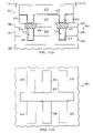
- FIGS. 11 a , 11 b , and 11 c show cross-sectional views ( FIG. 11 a ) and top views ( FIGS. 11 b and 11 c ) of the novel deep trench isolation structures 216 / 316 / 416 / 516 described herein implemented in a flash memory cell design.
- the semiconductor device 600 includes a workpiece 602 having an N well 604 and a P well 606 formed therein.
- Source and drain region 608 is disposed over the P well 606 .
- the flash memory cells include a floating gate 670 , an inter-gate oxide 672 , and a control gate electrode 674 .
- Deep trench isolation structures 616 (e.g., comprising deep trench isolation structures 216 / 316 / 416 / 516 described herein) are formed between the flash memory cells to provide isolation.
- a shallow trench isolation structure 614 is formed at the top of each deep trench isolation structure 616 .
- FIG. 11 b shows a top view of the flash memory cell 680 after the front end of line (FEOL) manufacturing process for the structure
- FIG. 11 c shows a top view of the flash memory cell 680 after the back end of line (BEOL), or metallization layer processing, for example.
- the metal runs 676 and 678 connect the drain 608 and source 608 to a contact layer 682 in the metallization structure, for example.
- FIG. 12 of the present patent application corresponds to FIG. 5 of U.S. Pat. No. 6,909,139.
- FIG. 12 shows a typical floating gate structure that includes an insulating tunnel oxide layer 63 (typically thin SiO 2 or oxynitride) on the surface of the substrate 40 (e.g., comprising a workpiece such as workpiece 202 shown in FIG. 2 of the present patent application), a first conductive, charge storage layer on the insulating layer that forms the floating gate 62 , an insulating layer 61 (typically an ONO layer) on the lower conductive layer, and a second conductive layer on the charge storage layer that forms the control gate 60 .
- a charge may be stored or erased from the floating gate transistor, or the charging state will be sensed in the read mode.
- Source regions 22 , 27 , 32 , 37 and others are formed by implanting the substrate with suitable N-type dopants and diffusing the dopants into the P-wells 42 .
- the deep trenches prevent the sources from laterally spreading into adjacent columns.
- the sources are further masked and self-aligned to spacers 91 , 92 .
- a P-type implant is made into the opening between spacers 91 , 92 to form P + body ties 24 in the source regions.
- each source is diffused via n ⁇ /P + body tie to provide a continuous, buried bit line 14 in the common P-well 42 .
- This buried bit line resistance is further reduced by subsequent silicide process prior to contact formation.
- Such silicidation must take place in the P + 24 overlap of the n ⁇ region, extend to both ends of n ⁇ region 22 and 27 but avoid extend to under the gate edge.
- Not every combined source region has a contact by a metal strap. It is sufficient to form contact with an upper level metal strap every thirty-two or sixty-four word lines (not shown) to reduce well resistance while maintaining single metal line per bit line simplicity.
- the added upper level of metal is simple to add, and does not adversely affect the footprint of the embedded memory array because its core processor already uses many levels of metals.
- the transistors in a typical cell of the array are shown in FIG. 12 , which again corresponds to FIG. 5 of U.S. Pat. No. 6,909,139.
- the substrate 40 has a deep N-well 41 and a shallow P-well 42 .
- the transistors are in the P-well 42 .
- Drain contacts 50 , 52 extend above the substrate 40 to contact a raised metal bit line 500 , as shown in FIG. 13 .
- Source regions 22 , 27 form buried bit lines 14 that are vertically aligned with the raised metal bit lines.
- a higher (upper level) metal line runs in parallel with and above drain bit line 500 and contacts the source buried bit lines 14 .
- the sources, drains and control gates are silicided. Sidewall oxide and spacers isolate the gates from the drains and sources.
- the deep trenches isolation structures 216 / 316 / 416 / 516 / 616 separate adjacent columns and buried bit lines 14 from each other.
- the novel deep trenches 216 / 316 / 416 / 516 / 616 described herein provide improved lateral isolation of adjacent doped wells and improved isolation from substrates, by increasing the threshold voltage above which a deep trench isolation structure 216 / 316 / 416 / 516 / 616 begins to function as a parasitic transistor.
- FIGS. 15 and 16 which correspond to FIGS. 9 and 10, respectively, of U.S. Pat. No. 6,909,139, the steps involved in fabricating the deep trench 46 in which the deep trench isolation structures 216 / 316 / 416 / 516 / 616 of embodiments of the present invention are formed are shown.
- the deep trench 46 is formed and filled in accordance with embodiments of the present invention to form deep trench isolation structures 216 / 316 / 416 / 516 / 616 at the beginning of the process, generally before the shallow trench isolation that is used to separate the high voltage and CMOS devices is formed.
- a pad oxide layer 70 is deposited on the substrate 40 , as shown in FIG. 15 .
- the pad oxide is approximately 53 Angstroms thick.
- a pad nitride layer 71 with a thickness of about 1800 Angstroms is deposited over the pad oxide layer.
- a layer of boron-doped silicon glass (BSG) 72 is deposited on the pad nitride layer 71 .
- the BSG 72 is patterned by a photoresist mask 77 .
- the mask 77 provides openings 46 that will ultimately become the deep trench shown in FIG. 15 .
- the BSG 72 is removed from the trench followed by resist strip and clean that leaves BSG on the active region as a hard mask to protect the substrate from the subsequent deep trench etch.
- the trench is filled as described herein to form deep trench isolation structures 216 / 316 / 416 / 516 / 616 , wherein a structure which causes the threshold voltage of the parasitic transistor to increase is formed in the deep trench isolation regions.
- Embodiments of the present invention are preferably implemented at the point in the manufacturing process for a flash memory cell shown in FIG. 16 , after the formation of the trench.
- a channel stop region may be implanted into the bottom surface of the deep trench 40 , a bottom portion of the deep trench 40 may be partially filled with an insulating material, or a doped polysilicon fill material may be disposed within the deep trench 40 .
- combinations of these techniques may be used in order to increase the threshold voltage above which the deep trench isolation structure 216 / 316 / 416 / 516 / 616 begins to function as a parasitic transistor.
- the fabrication of the semiconductor device 700 is then continued to complete the device, for example.
- FIG. 17 A more detailed view of an example of a completed flash memory cell structure 700 having the novel deep trench isolation structures 216 / 316 / 416 / 516 / 616 described herein, and in which embodiments of the present invention may be implemented, is shown in FIG. 17 , which corresponds to FIG. 19 of U.S. Pat. No. 6,909,139.
- the methods of forming the structure shown in FIG. 17 may comprise the methods described with reference to FIG. 12 through 19 of U.S. Pat. No. 6,909,139.
- the P-type substrate 40 is suitably patterned to form shallow trench isolation regions. The trench isolation regions isolate each pair of CMOS transistors and any linear or high voltage devices formed on the substrate.
- the deep trenches separate the memory columns from each other and from the other devices.
- the substrate 40 is then covered with a floating gate oxide followed by a layer of polysilicon.
- a suitable portion of the substrate Prior to deposition of the layers, a suitable portion of the substrate, such as region A, is separately patterned and implanted to have a triple-well comprising N-well 41 that encloses P-well 42 .
- a logic CMOS pair of transistors are in region B.
- the B regions may include transistors other than CMOS logic pairs.
- transistor of one conductivity type may be formed in the B regions and the types of transistors may be logic or linear, including and not limited to power transistors such as LDMOS transistors.
- the oxide and polysilicon layers are then patterned with photoresist to form a floating gate slit (parallel to the bit line).
- a layer of ONO interpoly dielectric is deposited over the substrate.
- the layer comprises sequentially a thermally grown bottom oxide, a deposited layer of low temperature deposited polysilicon that is re-oxidized to form top oxide at a later time.
- the layer is suitably patterned by photoresist to form two of the three layers of the ONO interpoly dielectric in the EEPROM stack.
- the layer and polysilicon layer are stripped from the peripheral regions B and they are suitably patterned and implanted to form P-wells 42 and N-wells 41 .
- the substrate 40 is covered with a layer of oxide followed by a second layer of polysilicon 126 .
- the layer of oxide forms the gate oxide layer for the logic and linear devices and forms the upper oxide layer of the ONO dielectric layer.
- the polysilicon layer 126 is patterned and etched to form the control gates of the EEPROM transistors and the logic and linear transistors.
- a first TEOS layer is deposited over the second polysilicon layer.
- the first TEOS layer is then suitably patterned with photoresist to open the source and drain regions of the EEPROM. Source and drain regions are suitably implanted to form the source and drains of the EEPROM.
- the first TEOS layer is removed by a highly selective reactive ion etching process, stopping on polysilicon layer 126 .
- the sidewalls of the gate stack of the EEPROM are oxidized to provide a sidewall oxide suitable for flash stack transistors.
- the oxidation may take place at about 850 to 950° C. in a furnace for approximately 30 minutes in order to grow a sidewall that is about 15 manometers thick on the polysilicon regions of the gate stack, for example, although other oxidation parameters may also be used.
- a second TEOS layer is deposited over the substrate 40 .
- TEOS layer is suitably patterned with a photoresist layer to form the gates and to open the source and drains of the logic and linear transistors, as shown in FIG. 17 .
- the sources and drains of the logic and/or linear transistors are implanted, the second TEOS layer is removed by reactive ion etching and the gates of the peripheral transistors receive a thinner sidewall oxide.
- the sidewall oxide is approximately 6 nanometers thick and may be generated by a relatively short rapid thermal annealing step, for example.
- the rapid thermal annealing (RTA) may be carried out at about 700 to 900° C. for about 10 to 20 seconds, although the RTA may also comprise other parameters.
- the RTA activates the doping in the logic and/or linear transistors but does not drive them very far into the substrate. This results in a logic and/or linear region with relatively closely spaced transistors.
- the substrate is masked to expose only selected source regions in the memory array.
- the source regions are exposed and implanted with a P-type implant to form the P+ body ties, to the source N ⁇ junctions of the memory.
- Additional metal straps from upper levels of metal e.g., metallization layer M3 will bring the source rail resistance down. Not every source region requires a metal strap, and every thirty-second or sixty-fourth source region is sufficient. There is no bit line pitch increase due to the addition of metal strap M3 since both the M1 bit line and M3 source lines run on top of each other.
- the triple well allows the user to control the voltage on the deep buried N-well 41 and the shallow P-well 42 in order to program, erase, and read the array.
- a typical set of operating parameters for the flash memory cell to program, erase, and read appears in the following Table 1, where the voltages applied to the selected and unselected components are identified.
- the word line associated with the transistor is raised to approximately 2.5 volts.
- the bit line connected to the drain is coupled to a voltage of approximately 1.25 volts.
- the output of the cell then appears on the other or source bit line.
- the deep N well is held at zero volts.
- the voltages for all of the other electrodes of the rest of the array are set to zero volts.
- the word line of the gate with the selected transistor is raised to +14 volts.
- the drain bit line is lowered to ⁇ 3 volts, as is the buried source bit line, to provide a uniform voltage across the channel.
- the deep N well 41 is set to a positive voltage, such as +3 volts, as an example, to raise the body effect of the parasitic transistor and thus eliminate the parasitic leakage from the adjacent columns of cells. Setting the deep N well 41 to a positive voltage biases the N well 41 , suppressing leakage current from the shallow P well 42 to the deep N well 41 , for example.
- the gates of the unselected transistors are either set to zero or ⁇ 3 volts and the other electrodes are set to +3 volts.
- the drain and the source bit lines are set to +3 volts and the gate is set to ⁇ 14 volts.
- the gates of the unselected transistors are set to between zero and +3 volts and all of the other electrodes are set to +3 volts.
- Embodiments of the present invention may also be implemented in other applications where deep trenches are used to separate active areas from one another, for example.
- Advantages of embodiments of the invention include increasing the threshold voltage above which a deep trench isolation structure 216 / 316 / 416 / 516 / 616 begins to function as a parasitic transistor, increasing device performance and improving the isolation capabilities of the deep trench isolation structure 216 / 316 / 416 / 516 / 616 .
- Improved lateral isolation is provided by the novel deep trench isolation structures 216 / 316 / 416 / 516 / 616 described herein.
- the isolation structures 216 / 316 / 416 / 516 / 616 provide improved lateral isolation of adjacent doped wells and improved isolation from substrates.
- the deep trenches may isolate two adjacent P wells embedded in a triple well, e.g., disposed above a buried N well, isolating the P wells and N well from the P doped substrate. This allows for different biases to be applied to the P wells, for example.
- the threshold voltage of parasitic transistors in the deep trench isolation structure 216 / 316 / 416 / 516 / 616 can be increased by about 5 to 10 V or greater, for example, by the use of embodiments of the present invention.
- the adjacent P wells are isolated (e.g., P wells 506 in FIG. 10 ). Therefore, adjacent P wells may be biased independently, which may optimize performance in some applications, for example.
- the doping may be achieved by an in-situ doping process in some embodiments, which is an advantage if the trenches for the deep trench isolation structures 216 / 316 / 416 / 516 / 616 are very deep and narrow, in which implantation of a dopant may be difficult, for example.
Abstract
Description
| U.S. Pat. | Filing | Issue | ||
| Ser. No. | No. | date | Date | Title |
| 10/234,344 | 6,841,824 | Sep. 4, | Jan. 11, | Flash Memory Cell and |
| B2 | 2002 | 2005 | the Method of Making | |
| Separate Sidewall | ||||
| Oxidation | ||||
| 10/607,610 | 6,909,139 | Jun. 27, | Jun. 21, | One Transistor Flash |
| B2 | 2003 | 2005 | Memory Cell | |
| 10/615,630 | 6,864,151 | Jul. 9, | Mar. 8, | Method of Forming |
| B2 | 2003 | 2005 | Shallow Trench Isolation | |
| Using Deep Trench | ||||
| Isolation | ||||
| 10/918,335 | — | Aug. 13, | — | Integrated Memory |
| 2004 | Device and Process | |||
| TABLE 1 | ||||
| Read (volts) | Program (volts) | Erase (volts) | ||
| Selected cells: | |||
| Gate | VPP = 2.5 | +14 | −14 |
| Drain | VDD = 1.25 | −3 | +3 |
| Source/P-well | 0 | −3 | +3 |
| Deep N-well | 0 | +3 | +3 |
| Unselected cells: | |||
| Gate | 0 | 0/−3 | 0/+3 |
| Drain disturb | DR turn-on | ||
| Drain | 0 | +3 | +3 |
| Gate disturb | R. disturb | ||
| Source/P-well | 0 | +3 | +3 |
| Deep N-well | 0 | +3 | +3 |
Claims (25)
Priority Applications (4)
| Application Number | Priority Date | Filing Date | Title |
|---|---|---|---|
| US11/367,247 US7679130B2 (en) | 2005-05-10 | 2006-03-03 | Deep trench isolation structures and methods of formation thereof |
| TW095115512A TWI339897B (en) | 2005-05-10 | 2006-05-01 | Deep trench isolation structures and methods of formation thereof |
| DE102006021070.0A DE102006021070B4 (en) | 2005-05-10 | 2006-05-05 | Semiconductor devices with deep trench isolation structures and methods of making same |
| US12/702,368 US8258028B2 (en) | 2005-05-10 | 2010-02-09 | Deep trench isolation structures and methods of formation thereof |
Applications Claiming Priority (2)
| Application Number | Priority Date | Filing Date | Title |
|---|---|---|---|
| US67933405P | 2005-05-10 | 2005-05-10 | |
| US11/367,247 US7679130B2 (en) | 2005-05-10 | 2006-03-03 | Deep trench isolation structures and methods of formation thereof |
Related Child Applications (1)
| Application Number | Title | Priority Date | Filing Date |
|---|---|---|---|
| US12/702,368 Division US8258028B2 (en) | 2005-05-10 | 2010-02-09 | Deep trench isolation structures and methods of formation thereof |
Publications (2)
| Publication Number | Publication Date |
|---|---|
| US20060267134A1 US20060267134A1 (en) | 2006-11-30 |
| US7679130B2 true US7679130B2 (en) | 2010-03-16 |
Family
ID=37295598
Family Applications (2)
| Application Number | Title | Priority Date | Filing Date |
|---|---|---|---|
| US11/367,247 Active 2028-06-11 US7679130B2 (en) | 2005-05-10 | 2006-03-03 | Deep trench isolation structures and methods of formation thereof |
| US12/702,368 Active US8258028B2 (en) | 2005-05-10 | 2010-02-09 | Deep trench isolation structures and methods of formation thereof |
Family Applications After (1)
| Application Number | Title | Priority Date | Filing Date |
|---|---|---|---|
| US12/702,368 Active US8258028B2 (en) | 2005-05-10 | 2010-02-09 | Deep trench isolation structures and methods of formation thereof |
Country Status (3)
| Country | Link |
|---|---|
| US (2) | US7679130B2 (en) |
| DE (1) | DE102006021070B4 (en) |
| TW (1) | TWI339897B (en) |
Cited By (6)
| Publication number | Priority date | Publication date | Assignee | Title |
|---|---|---|---|---|
| US8637365B2 (en) | 2012-06-06 | 2014-01-28 | International Business Machines Corporation | Spacer isolation in deep trench |
| US8927989B2 (en) | 2012-11-28 | 2015-01-06 | International Business Machines Corporation | Voltage contrast inspection of deep trench isolation |
| US20150137309A1 (en) * | 2006-03-01 | 2015-05-21 | Infineon Technologies Ag | Methods of Fabricating Isolation Regions of Semiconductor Devices and Structures Thereof |
| US10504768B1 (en) * | 2018-06-28 | 2019-12-10 | Globalfoundries Singapore Pte. Ltd. | Contact structures to deep trench isolation structures and method of nanufacturing the same |
| US10529866B2 (en) | 2012-05-30 | 2020-01-07 | X-Fab Semiconductor Foundries Gmbh | Semiconductor device |
| US11682578B2 (en) | 2020-07-30 | 2023-06-20 | Taiwan Semiconductor Manufacturing Co., Ltd. | Multilayer isolation structure for high voltage silicon-on-insulator device |
Families Citing this family (20)
| Publication number | Priority date | Publication date | Assignee | Title |
|---|---|---|---|---|
| US20070140008A1 (en) * | 2005-12-21 | 2007-06-21 | Microchip Technology Incorporated | Independently programmable memory segments within an NMOS electrically erasable programmable read only memory array achieved by P-well separation and method therefor |
| US7982284B2 (en) | 2006-06-28 | 2011-07-19 | Infineon Technologies Ag | Semiconductor component including an isolation structure and a contact to the substrate |
| US7816759B2 (en) * | 2008-01-09 | 2010-10-19 | Infineon Technologies Ag | Integrated circuit including isolation regions substantially through substrate |
| JP2011077185A (en) * | 2009-09-29 | 2011-04-14 | Elpida Memory Inc | Semiconductor device, method of manufacturing semiconductor device, and data processing system |
| US9484269B2 (en) | 2010-06-24 | 2016-11-01 | Globalfoundries Inc. | Structure and method to control bottom corner threshold in an SOI device |
| KR101201903B1 (en) * | 2010-07-20 | 2012-11-16 | 매그나칩 반도체 유한회사 | Element isolation structure of semiconductor and method for forming the same |
| US8138558B2 (en) * | 2010-08-20 | 2012-03-20 | Great Wall Semiconductor Corporation | Semiconductor device and method of forming low voltage MOSFET for portable electronic devices and data processing centers |
| CN102446968A (en) * | 2010-10-13 | 2012-05-09 | 上海华虹Nec电子有限公司 | LDMOS (Laterally Diffused Metal Oxide Semiconductor) device structure and manufacturing method |
| US8710627B2 (en) * | 2011-06-28 | 2014-04-29 | Alpha And Omega Semiconductor Incorporated | Uni-directional transient voltage suppressor (TVS) |
| US9698044B2 (en) | 2011-12-01 | 2017-07-04 | Taiwan Semiconductor Manufacturing Company, Ltd. | Localized carrier lifetime reduction |
| US20130221478A1 (en) * | 2012-02-27 | 2013-08-29 | Globalfoundries Inc. | Methods of forming isolation structures for semiconductor devices by employing a spin-on glass material or a flowable oxide material |
| US9082654B2 (en) * | 2013-05-30 | 2015-07-14 | Rohm Co., Ltd. | Method of manufacturing non-volatile memory cell with simplified step of forming floating gate |
| US9406710B2 (en) | 2013-11-11 | 2016-08-02 | United Microelectronics Corp. | Semiconductor device and manufacturing method of the same |
| FR3060201B1 (en) * | 2016-12-12 | 2019-05-17 | Aledia | ELECTRONIC DEVICE COMPRISING A TRENCH OF ELECTRICAL INSULATION AND METHOD OF MANUFACTURING THE SAME |
| US9955225B1 (en) | 2017-03-31 | 2018-04-24 | At&T Mobility Ii Llc | Sharing video content from a set top box through a mobile phone |
| US11127622B2 (en) | 2020-01-13 | 2021-09-21 | Nxp Usa, Inc. | Deep trench isolation and substrate connection on SOI |
| US11177158B2 (en) * | 2020-02-25 | 2021-11-16 | Globalfoundries U.S. Inc. | Integrated circuit structure with semiconductor-based isolation structure and methods to form same |
| CN111354677B (en) * | 2020-03-09 | 2023-10-20 | 上海华虹宏力半导体制造有限公司 | Preparation method of deep trench isolation structure and semiconductor device |
| CN111968975A (en) * | 2020-08-07 | 2020-11-20 | 长江存储科技有限责任公司 | Circuit chip, three-dimensional memory and method for preparing three-dimensional memory |
| US11443976B2 (en) * | 2020-10-20 | 2022-09-13 | Taiwan Semiconductor Manufacturing Company, Ltd. | Trench isolation process |
Citations (58)
| Publication number | Priority date | Publication date | Assignee | Title |
|---|---|---|---|---|
| US4549927A (en) | 1984-06-29 | 1985-10-29 | International Business Machines Corporation | Method of selectively exposing the sidewalls of a trench and its use to the forming of a metal silicide substrate contact for dielectric filled deep trench isolated devices |
| US4692992A (en) | 1986-06-25 | 1987-09-15 | Rca Corporation | Method of forming isolation regions in a semiconductor device |
| US4835115A (en) | 1987-12-07 | 1989-05-30 | Texas Instruments Incorporated | Method for forming oxide-capped trench isolation |
| JPH02260564A (en) | 1989-03-31 | 1990-10-23 | Mitsubishi Electric Corp | Semiconductor device and manufacture thereof |
| US4994406A (en) | 1989-11-03 | 1991-02-19 | Motorola Inc. | Method of fabricating semiconductor devices having deep and shallow isolation structures |
| US5296392A (en) * | 1990-03-06 | 1994-03-22 | Digital Equipment Corporation | Method of forming trench isolated regions with sidewall doping |
| US5306940A (en) | 1990-10-22 | 1994-04-26 | Nec Corporation | Semiconductor device including a locos type field oxide film and a U trench penetrating the locos film |
| US5313419A (en) | 1993-02-01 | 1994-05-17 | National Semiconductor Corporation | Self-aligned trench isolation scheme for select transistors in an alternate metal virtual ground (AMG) EPROM array |
| US5468676A (en) | 1992-09-23 | 1995-11-21 | Texas Instruments Incorporated | Trench isolation structure and method for forming |
| US5471422A (en) | 1994-04-11 | 1995-11-28 | Motorola, Inc. | EEPROM cell with isolation transistor and methods for making and operating the same |
| US5635415A (en) | 1994-11-30 | 1997-06-03 | United Microelectronics Corporation | Method of manufacturing buried bit line flash EEPROM memory cell |
| US5644532A (en) | 1992-09-08 | 1997-07-01 | National Semiconductor Corporation | Method for programming a cell in a source-coupling, split-gate, virtual ground flash EEPROM array |
| EP0810667A2 (en) | 1996-05-30 | 1997-12-03 | Hyundai Electronics America, Inc. | Triple well flash memory cell and fabrication process |
| US5702988A (en) | 1996-05-02 | 1997-12-30 | Taiwan Semiconductor Manufacturing Company, Ltd. | Blending integrated circuit technology |
| US5717634A (en) | 1995-07-19 | 1998-02-10 | Texas Instruments Incorporated | Programmable and convertible non-volatile memory array |
| EP0926728A1 (en) | 1997-12-25 | 1999-06-30 | Matsushita Electronics Corporation | Method of manufacturing a BiCMOS semiconductor device |
| US6037222A (en) | 1998-05-22 | 2000-03-14 | Taiwan Semiconductor Manufacturing Company | Method for fabricating a dual-gate dielectric module for memory embedded logic using salicide technology and polycide technology |
| EP0997930A1 (en) | 1998-10-30 | 2000-05-03 | Halo Lsi Design and Device Technology Inc. | Integration method for sidewall split gate flash transistor |
| US6096597A (en) | 1997-01-31 | 2000-08-01 | Texas Instruments Incorporated | Method for fabricating an integrated circuit structure |
| US6141242A (en) | 1997-04-14 | 2000-10-31 | International Business Machines Corporation | Low cost mixed memory integration with substantially coplanar gate surfaces |
| US6146970A (en) | 1998-05-26 | 2000-11-14 | Motorola Inc. | Capped shallow trench isolation and method of formation |
| US6180456B1 (en) | 1999-02-17 | 2001-01-30 | International Business Machines Corporation | Triple polysilicon embedded NVRAM cell and method thereof |
| US6184107B1 (en) | 1999-03-17 | 2001-02-06 | International Business Machines Corp. | Capacitor trench-top dielectric for self-aligned device isolation |
| US6207501B1 (en) | 1998-12-15 | 2001-03-27 | United Microelectronics. Corp. | Method of fabricating a flash memory |
| US6214696B1 (en) | 1998-04-22 | 2001-04-10 | Texas Instruments - Acer Incorporated | Method of fabricating deep-shallow trench isolation |
| US6228712B1 (en) | 1998-11-10 | 2001-05-08 | Mitsubishi Denki Kabushiki Kaisha | Non-volatile semiconductor memory device and manufacturing method thereof |
| US6251734B1 (en) | 1998-07-01 | 2001-06-26 | Motorola, Inc. | Method for fabricating trench isolation and trench substrate contact |
| US6258667B1 (en) | 1999-08-10 | 2001-07-10 | United Microelectronics Corp. | Method for implementing embedded flash |
| US6284602B1 (en) | 1999-09-20 | 2001-09-04 | Advanced Micro Devices, Inc. | Process to reduce post cycling program VT dispersion for NAND flash memory devices |
| US6284593B1 (en) | 2000-11-03 | 2001-09-04 | International Business Machines Corporation | Method for shallow trench isolated, contacted well, vertical MOSFET DRAM |
| US6297127B1 (en) | 2000-06-22 | 2001-10-02 | International Business Machines Corporation | Self-aligned deep trench isolation to shallow trench isolation |
| US6303413B1 (en) * | 2000-05-03 | 2001-10-16 | Maxim Integrated Products, Inc. | Method of forming a shallow and deep trench isolation (SDTI) suitable for silicon on insulator (SOI) substrates |
| US6307781B1 (en) | 1999-09-30 | 2001-10-23 | Infineon Technologies Aktiengesellschaft | Two transistor flash memory cell |
| US6327182B1 (en) | 1998-06-22 | 2001-12-04 | Motorola Inc. | Semiconductor device and a method of operation the same |
| WO2002015190A2 (en) | 2000-08-15 | 2002-02-21 | Motorola, Inc., A Corporation Of The State Of Delaware | Non-volatile memory, method of manufacture and programming |
| US6368907B1 (en) | 1999-11-29 | 2002-04-09 | Matsushita Electric Industrial Co., Ltd. | Method of fabricating semiconductor device |
| EP1209749A1 (en) | 2000-05-12 | 2002-05-29 | Matsushita Electric Industrial Co., Ltd. | Semiconductor device and method of manufacture thereof |
| US6406960B1 (en) | 1999-10-25 | 2002-06-18 | Advanced Micro Devices, Inc. | Process for fabricating an ONO structure having a silicon-rich silicon nitride layer |
| US6559008B2 (en) | 2001-10-04 | 2003-05-06 | Hynix Semiconductor America, Inc. | Non-volatile memory cells with selectively formed floating gate |
| US6566197B2 (en) | 2000-08-29 | 2003-05-20 | Hynix Semiconductor Inc. | Method for fabricating connection structure between segment transistor and memory cell region of flash memory device |
| US6600199B2 (en) | 2000-12-29 | 2003-07-29 | International Business Machines Corporation | Deep trench-buried layer array and integrated device structures for noise isolation and latch up immunity |
| US6628544B2 (en) | 1999-09-30 | 2003-09-30 | Infineon Technologies Ag | Flash memory cell and method to achieve multiple bits per cell |
| EP1351292A2 (en) | 2002-04-05 | 2003-10-08 | Sharp Kabushiki Kaisha | Semiconductor device comprising a flexible region and method for manufacturing the same |
| US6667226B2 (en) | 2000-12-22 | 2003-12-23 | Texas Instruments Incorporated | Method and system for integrating shallow trench and deep trench isolation structures in a semiconductor device |
| US6693830B1 (en) | 2001-10-22 | 2004-02-17 | Lattice Semiconductor Corp. | Single-poly two-transistor EEPROM cell with differentially doped floating gate |
| WO2004023553A2 (en) | 2002-09-02 | 2004-03-18 | Infineon Technologies Ag | Bitline structure and method for production thereof |
| US20040183159A1 (en) | 2003-03-17 | 2004-09-23 | Hitachi, Ltd. | Semiconductor device |
| US6806540B2 (en) | 2000-10-11 | 2004-10-19 | Kabushiki Kaisha Toshiba | Semiconductor device and method of manufacturing the same |
| US6815311B2 (en) | 2001-08-30 | 2004-11-09 | Hynix Semiconductor Inc. | Method for fabricating semiconductor memory device |
| US6841824B2 (en) | 2002-09-04 | 2005-01-11 | Infineon Technologies Ag | Flash memory cell and the method of making separate sidewall oxidation |
| US6844588B2 (en) | 2001-12-19 | 2005-01-18 | Freescale Semiconductor, Inc. | Non-volatile memory |
| US20050045944A1 (en) | 2003-02-14 | 2005-03-03 | Achim Gratz | Semiconductor circuit arrangement with trench isolation and fabrication method |
| US6864530B2 (en) | 2002-03-05 | 2005-03-08 | Hynix Semiconductor America, Inc. | High density flash memory architecture with columnar substrate coding |
| US6864151B2 (en) | 2003-07-09 | 2005-03-08 | Infineon Technologies Ag | Method of forming shallow trench isolation using deep trench isolation |
| US6885080B2 (en) | 2002-02-22 | 2005-04-26 | International Business Machines Corporation | Deep trench isolation of embedded DRAM for improved latch-up immunity |
| US6909139B2 (en) | 2003-06-27 | 2005-06-21 | Infineon Technologies Ag | One transistor flash memory cell |
| US20050179111A1 (en) * | 2004-02-12 | 2005-08-18 | Iwen Chao | Semiconductor device with low resistive path barrier |
| US20060033145A1 (en) | 2004-08-13 | 2006-02-16 | Ronald Kakoschke | Integrated memory device and process |
Family Cites Families (13)
| Publication number | Priority date | Publication date | Assignee | Title |
|---|---|---|---|---|
| US4526631A (en) * | 1984-06-25 | 1985-07-02 | International Business Machines Corporation | Method for forming a void free isolation pattern utilizing etch and refill techniques |
| EP0220108A3 (en) * | 1985-10-07 | 1990-04-11 | Thomson Components-Mostek Corporation | Side-wall doping for trench isolation |
| US4808543A (en) * | 1986-05-07 | 1989-02-28 | Motorola, Inc. | Well Extensions for trench devices |
| US5382541A (en) * | 1992-08-26 | 1995-01-17 | Harris Corporation | Method for forming recessed oxide isolation containing deep and shallow trenches |
| US5559008A (en) * | 1992-11-05 | 1996-09-24 | Cornell Research Foundation, Inc. | Leukotoxin gene from Pasteurella suis |
| US6069597A (en) * | 1997-08-29 | 2000-05-30 | Candescent Technologies Corporation | Circuit and method for controlling the brightness of an FED device |
| KR20010059185A (en) | 1999-12-30 | 2001-07-06 | 박종섭 | A method for forming a field oxide of a semiconductor device |
| KR100346844B1 (en) | 2000-12-09 | 2002-08-03 | 삼성전자 주식회사 | Semiconductor device having shallow trench isolation structure and method for manufacturing the same |
| JP2003297848A (en) * | 2002-04-01 | 2003-10-17 | Matsushita Electric Ind Co Ltd | Method of manufacturing semiconductor device |
| US6933203B2 (en) * | 2002-11-19 | 2005-08-23 | Texas Instruments Incorporated | Methods for improving well to well isolation |
| TW594912B (en) | 2002-11-22 | 2004-06-21 | Taiwan Semiconductor Mfg | Fabrication method of shallow and deep trench isolation structure |
| KR100525797B1 (en) | 2003-06-18 | 2005-11-02 | 동부아남반도체 주식회사 | STI structure and processing method |
| US7015086B2 (en) * | 2004-02-05 | 2006-03-21 | Taiwan Semiconductor Manufacturing Company, Ltd. | Method of forming a shallow trench-deep trench isolation region for a BiCMOS/CMOS technology |
-
2006
- 2006-03-03 US US11/367,247 patent/US7679130B2/en active Active
- 2006-05-01 TW TW095115512A patent/TWI339897B/en active
- 2006-05-05 DE DE102006021070.0A patent/DE102006021070B4/en not_active Expired - Fee Related
-
2010
- 2010-02-09 US US12/702,368 patent/US8258028B2/en active Active
Patent Citations (59)
| Publication number | Priority date | Publication date | Assignee | Title |
|---|---|---|---|---|
| US4549927A (en) | 1984-06-29 | 1985-10-29 | International Business Machines Corporation | Method of selectively exposing the sidewalls of a trench and its use to the forming of a metal silicide substrate contact for dielectric filled deep trench isolated devices |
| US4692992A (en) | 1986-06-25 | 1987-09-15 | Rca Corporation | Method of forming isolation regions in a semiconductor device |
| US4835115A (en) | 1987-12-07 | 1989-05-30 | Texas Instruments Incorporated | Method for forming oxide-capped trench isolation |
| JPH02260564A (en) | 1989-03-31 | 1990-10-23 | Mitsubishi Electric Corp | Semiconductor device and manufacture thereof |
| US4994406A (en) | 1989-11-03 | 1991-02-19 | Motorola Inc. | Method of fabricating semiconductor devices having deep and shallow isolation structures |
| US5296392A (en) * | 1990-03-06 | 1994-03-22 | Digital Equipment Corporation | Method of forming trench isolated regions with sidewall doping |
| US5306940A (en) | 1990-10-22 | 1994-04-26 | Nec Corporation | Semiconductor device including a locos type field oxide film and a U trench penetrating the locos film |
| US5644532A (en) | 1992-09-08 | 1997-07-01 | National Semiconductor Corporation | Method for programming a cell in a source-coupling, split-gate, virtual ground flash EEPROM array |
| US5468676A (en) | 1992-09-23 | 1995-11-21 | Texas Instruments Incorporated | Trench isolation structure and method for forming |
| US5313419A (en) | 1993-02-01 | 1994-05-17 | National Semiconductor Corporation | Self-aligned trench isolation scheme for select transistors in an alternate metal virtual ground (AMG) EPROM array |
| US5471422A (en) | 1994-04-11 | 1995-11-28 | Motorola, Inc. | EEPROM cell with isolation transistor and methods for making and operating the same |
| US5635415A (en) | 1994-11-30 | 1997-06-03 | United Microelectronics Corporation | Method of manufacturing buried bit line flash EEPROM memory cell |
| US5717634A (en) | 1995-07-19 | 1998-02-10 | Texas Instruments Incorporated | Programmable and convertible non-volatile memory array |
| US5702988A (en) | 1996-05-02 | 1997-12-30 | Taiwan Semiconductor Manufacturing Company, Ltd. | Blending integrated circuit technology |
| EP0810667A2 (en) | 1996-05-30 | 1997-12-03 | Hyundai Electronics America, Inc. | Triple well flash memory cell and fabrication process |
| US6096597A (en) | 1997-01-31 | 2000-08-01 | Texas Instruments Incorporated | Method for fabricating an integrated circuit structure |
| US6141242A (en) | 1997-04-14 | 2000-10-31 | International Business Machines Corporation | Low cost mixed memory integration with substantially coplanar gate surfaces |
| EP0926728A1 (en) | 1997-12-25 | 1999-06-30 | Matsushita Electronics Corporation | Method of manufacturing a BiCMOS semiconductor device |
| US6214696B1 (en) | 1998-04-22 | 2001-04-10 | Texas Instruments - Acer Incorporated | Method of fabricating deep-shallow trench isolation |
| US6037222A (en) | 1998-05-22 | 2000-03-14 | Taiwan Semiconductor Manufacturing Company | Method for fabricating a dual-gate dielectric module for memory embedded logic using salicide technology and polycide technology |
| US6146970A (en) | 1998-05-26 | 2000-11-14 | Motorola Inc. | Capped shallow trench isolation and method of formation |
| US6327182B1 (en) | 1998-06-22 | 2001-12-04 | Motorola Inc. | Semiconductor device and a method of operation the same |
| US6251734B1 (en) | 1998-07-01 | 2001-06-26 | Motorola, Inc. | Method for fabricating trench isolation and trench substrate contact |
| EP0997930A1 (en) | 1998-10-30 | 2000-05-03 | Halo Lsi Design and Device Technology Inc. | Integration method for sidewall split gate flash transistor |
| US6228712B1 (en) | 1998-11-10 | 2001-05-08 | Mitsubishi Denki Kabushiki Kaisha | Non-volatile semiconductor memory device and manufacturing method thereof |
| US6207501B1 (en) | 1998-12-15 | 2001-03-27 | United Microelectronics. Corp. | Method of fabricating a flash memory |
| US6180456B1 (en) | 1999-02-17 | 2001-01-30 | International Business Machines Corporation | Triple polysilicon embedded NVRAM cell and method thereof |
| US6184107B1 (en) | 1999-03-17 | 2001-02-06 | International Business Machines Corp. | Capacitor trench-top dielectric for self-aligned device isolation |
| US6258667B1 (en) | 1999-08-10 | 2001-07-10 | United Microelectronics Corp. | Method for implementing embedded flash |
| US6284602B1 (en) | 1999-09-20 | 2001-09-04 | Advanced Micro Devices, Inc. | Process to reduce post cycling program VT dispersion for NAND flash memory devices |
| US6628544B2 (en) | 1999-09-30 | 2003-09-30 | Infineon Technologies Ag | Flash memory cell and method to achieve multiple bits per cell |
| US6307781B1 (en) | 1999-09-30 | 2001-10-23 | Infineon Technologies Aktiengesellschaft | Two transistor flash memory cell |
| US6406960B1 (en) | 1999-10-25 | 2002-06-18 | Advanced Micro Devices, Inc. | Process for fabricating an ONO structure having a silicon-rich silicon nitride layer |
| US6368907B1 (en) | 1999-11-29 | 2002-04-09 | Matsushita Electric Industrial Co., Ltd. | Method of fabricating semiconductor device |
| US6303413B1 (en) * | 2000-05-03 | 2001-10-16 | Maxim Integrated Products, Inc. | Method of forming a shallow and deep trench isolation (SDTI) suitable for silicon on insulator (SOI) substrates |
| EP1209749A1 (en) | 2000-05-12 | 2002-05-29 | Matsushita Electric Industrial Co., Ltd. | Semiconductor device and method of manufacture thereof |
| US6297127B1 (en) | 2000-06-22 | 2001-10-02 | International Business Machines Corporation | Self-aligned deep trench isolation to shallow trench isolation |
| WO2002015190A2 (en) | 2000-08-15 | 2002-02-21 | Motorola, Inc., A Corporation Of The State Of Delaware | Non-volatile memory, method of manufacture and programming |
| US6438030B1 (en) | 2000-08-15 | 2002-08-20 | Motorola, Inc. | Non-volatile memory, method of manufacture, and method of programming |
| US6566197B2 (en) | 2000-08-29 | 2003-05-20 | Hynix Semiconductor Inc. | Method for fabricating connection structure between segment transistor and memory cell region of flash memory device |
| US6806540B2 (en) | 2000-10-11 | 2004-10-19 | Kabushiki Kaisha Toshiba | Semiconductor device and method of manufacturing the same |
| US6284593B1 (en) | 2000-11-03 | 2001-09-04 | International Business Machines Corporation | Method for shallow trench isolated, contacted well, vertical MOSFET DRAM |
| US6667226B2 (en) | 2000-12-22 | 2003-12-23 | Texas Instruments Incorporated | Method and system for integrating shallow trench and deep trench isolation structures in a semiconductor device |
| US6600199B2 (en) | 2000-12-29 | 2003-07-29 | International Business Machines Corporation | Deep trench-buried layer array and integrated device structures for noise isolation and latch up immunity |
| US6815311B2 (en) | 2001-08-30 | 2004-11-09 | Hynix Semiconductor Inc. | Method for fabricating semiconductor memory device |
| US6559008B2 (en) | 2001-10-04 | 2003-05-06 | Hynix Semiconductor America, Inc. | Non-volatile memory cells with selectively formed floating gate |
| US6693830B1 (en) | 2001-10-22 | 2004-02-17 | Lattice Semiconductor Corp. | Single-poly two-transistor EEPROM cell with differentially doped floating gate |
| US6844588B2 (en) | 2001-12-19 | 2005-01-18 | Freescale Semiconductor, Inc. | Non-volatile memory |
| US6885080B2 (en) | 2002-02-22 | 2005-04-26 | International Business Machines Corporation | Deep trench isolation of embedded DRAM for improved latch-up immunity |
| US6864530B2 (en) | 2002-03-05 | 2005-03-08 | Hynix Semiconductor America, Inc. | High density flash memory architecture with columnar substrate coding |
| EP1351292A2 (en) | 2002-04-05 | 2003-10-08 | Sharp Kabushiki Kaisha | Semiconductor device comprising a flexible region and method for manufacturing the same |
| WO2004023553A2 (en) | 2002-09-02 | 2004-03-18 | Infineon Technologies Ag | Bitline structure and method for production thereof |
| US6841824B2 (en) | 2002-09-04 | 2005-01-11 | Infineon Technologies Ag | Flash memory cell and the method of making separate sidewall oxidation |
| US20050045944A1 (en) | 2003-02-14 | 2005-03-03 | Achim Gratz | Semiconductor circuit arrangement with trench isolation and fabrication method |
| US20040183159A1 (en) | 2003-03-17 | 2004-09-23 | Hitachi, Ltd. | Semiconductor device |
| US6909139B2 (en) | 2003-06-27 | 2005-06-21 | Infineon Technologies Ag | One transistor flash memory cell |
| US6864151B2 (en) | 2003-07-09 | 2005-03-08 | Infineon Technologies Ag | Method of forming shallow trench isolation using deep trench isolation |
| US20050179111A1 (en) * | 2004-02-12 | 2005-08-18 | Iwen Chao | Semiconductor device with low resistive path barrier |
| US20060033145A1 (en) | 2004-08-13 | 2006-02-16 | Ronald Kakoschke | Integrated memory device and process |
Non-Patent Citations (4)
| Title |
|---|
| Chang, et al., "Fabrication Method of Shallow and Deep Trench Isolation Structure", Abstract of TW 594912 (B), Jun. 21, 2004, Application No. TW20020134134 20021122. |
| English translation of the Examination Notification Issued to Taiwan Patent Application No. 095115512, Jan. 9, 2009. |
| Li, C.-N. B., et al., "A Novel Uniform-Channel-Program-Erase (UCPE) Flash EEPROM Using an Isolated P-well Structue," IEDM 00, Apr. 2000, pp. 779-782, IEEE, Los Alamitos, CA. |
| Yang, E. C.-S., et al., "Novel Bi-Directional Tunneling Program/Erase NOR (BiNOR)-Type Flash EEPROM," IEEE Transactions on Electron Devices, Jun. 1999, pp. 1294-1296, vol. 46, No. 6, IEEE, Los Alamitos, CA. |
Cited By (9)
| Publication number | Priority date | Publication date | Assignee | Title |
|---|---|---|---|---|
| US20150137309A1 (en) * | 2006-03-01 | 2015-05-21 | Infineon Technologies Ag | Methods of Fabricating Isolation Regions of Semiconductor Devices and Structures Thereof |
| US9653543B2 (en) * | 2006-03-01 | 2017-05-16 | Infineon Technologies Ag | Methods of fabricating isolation regions of semiconductor devices and structures thereof |
| US10529866B2 (en) | 2012-05-30 | 2020-01-07 | X-Fab Semiconductor Foundries Gmbh | Semiconductor device |
| US8637365B2 (en) | 2012-06-06 | 2014-01-28 | International Business Machines Corporation | Spacer isolation in deep trench |
| US8754461B2 (en) | 2012-06-06 | 2014-06-17 | International Business Machines Corporation | Spacer isolation in deep trench |
| US8927989B2 (en) | 2012-11-28 | 2015-01-06 | International Business Machines Corporation | Voltage contrast inspection of deep trench isolation |
| US9293382B2 (en) | 2012-11-28 | 2016-03-22 | Globalfoundries Inc. | Voltage contrast inspection of deep trench isolation |
| US10504768B1 (en) * | 2018-06-28 | 2019-12-10 | Globalfoundries Singapore Pte. Ltd. | Contact structures to deep trench isolation structures and method of nanufacturing the same |
| US11682578B2 (en) | 2020-07-30 | 2023-06-20 | Taiwan Semiconductor Manufacturing Co., Ltd. | Multilayer isolation structure for high voltage silicon-on-insulator device |
Also Published As
| Publication number | Publication date |
|---|---|
| US20100203703A1 (en) | 2010-08-12 |
| TWI339897B (en) | 2011-04-01 |
| US20060267134A1 (en) | 2006-11-30 |
| US8258028B2 (en) | 2012-09-04 |
| DE102006021070B4 (en) | 2017-06-22 |
| TW200711123A (en) | 2007-03-16 |
| DE102006021070A1 (en) | 2006-11-16 |
Similar Documents
| Publication | Publication Date | Title |
|---|---|---|
| US7679130B2 (en) | Deep trench isolation structures and methods of formation thereof | |
| US10079316B2 (en) | Split gate embedded memory technology and method of manufacturing thereof | |
| US6909139B2 (en) | One transistor flash memory cell | |
| US8031532B2 (en) | Methods of operating embedded flash memory devices | |
| US9012968B2 (en) | Semiconductor non-volatile memory device | |
| US6177703B1 (en) | Method and apparatus for producing a single polysilicon flash EEPROM having a select transistor and a floating gate transistor | |
| US20070166912A1 (en) | Three-dimensional control-gate architecture for single poly EPROM memory devices fabricated in planar CMOS technology | |
| US20060214254A1 (en) | Semiconductor device and manufacturing method of the same | |
| US7163863B2 (en) | Vertical memory cell and manufacturing method thereof | |
| US7126188B2 (en) | Vertical split gate memory cell and manufacturing method thereof | |
| US6225161B1 (en) | Fully recessed semiconductor method for low power applications with single wrap around buried drain region | |
| US20060278933A1 (en) | Semiconductor device and manufacturing method thereof | |
| US20070111442A1 (en) | Method of making a multi-bit nanocrystal memory | |
| US20070241387A1 (en) | Nonvolatile semiconductor memory device | |
| US6844586B2 (en) | Fabrication of gate dielectric in nonvolatile memories having select, floating and control gates | |
| US9806087B2 (en) | Low cost high performance EEPROM device | |
| US20040217411A1 (en) | Non-volatile semiconductor memory device and manufacturing method therefor | |
| JP3860408B2 (en) | Semiconductor device and method for manufacturing semiconductor device | |
| JP4047500B2 (en) | Semiconductor device and manufacturing method thereof | |
| US6834011B2 (en) | Structure, fabrication method and operating method for flash memory |
Legal Events
| Date | Code | Title | Description |
|---|---|---|---|
| AS | Assignment |
Owner name: INFINEON TECHNOLOGIES NORTH AMERICA CORP.,CALIFORN Free format text: ASSIGNMENT OF ASSIGNORS INTEREST;ASSIGNORS:TILKE, ARMIN;SHUM, DANNY PAK-CHUM;SIGNING DATES FROM 20060216 TO 20060220;REEL/FRAME:017428/0492 Owner name: INFINEON TECHNOLOGIES AG, GERMANY Free format text: ASSIGNMENT OF ASSIGNORS INTEREST;ASSIGNORS:KAKOSCHKE, RONALD;PESCINI, LAURA;STRENZ, KARL ROBERT;AND OTHERS;REEL/FRAME:017428/0417;SIGNING DATES FROM 20060221 TO 20060222 Owner name: INFINEON TECHNOLOGIES AG,GERMANY Free format text: ASSIGNMENT OF ASSIGNORS INTEREST;ASSIGNORS:KAKOSCHKE, RONALD;PESCINI, LAURA;STRENZ, KARL ROBERT;AND OTHERS;SIGNING DATES FROM 20060221 TO 20060222;REEL/FRAME:017428/0417 Owner name: INFINEON TECHNOLOGIES NORTH AMERICA CORP., CALIFOR Free format text: ASSIGNMENT OF ASSIGNORS INTEREST;ASSIGNORS:TILKE, ARMIN;SHUM, DANNY PAK-CHUM;REEL/FRAME:017428/0492;SIGNING DATES FROM 20060216 TO 20060220 |
|
| AS | Assignment |
Owner name: INFINEON TECHNOLOGIES AG, GERMANY Free format text: ASSIGNMENT OF ASSIGNORS INTEREST;ASSIGNOR:INFINEON TECHNOLOGIES NORTH AMERICA CORP.;REEL/FRAME:017479/0018 Effective date: 20060417 Owner name: INFINEON TECHNOLOGIES AG,GERMANY Free format text: ASSIGNMENT OF ASSIGNORS INTEREST;ASSIGNOR:INFINEON TECHNOLOGIES NORTH AMERICA CORP.;REEL/FRAME:017479/0018 Effective date: 20060417 |
|
| FEPP | Fee payment procedure |
Free format text: PAYOR NUMBER ASSIGNED (ORIGINAL EVENT CODE: ASPN); ENTITY STATUS OF PATENT OWNER: LARGE ENTITY |
|
| STCF | Information on status: patent grant |
Free format text: PATENTED CASE |
|
| FPAY | Fee payment |
Year of fee payment: 4 |
|
| MAFP | Maintenance fee payment |
Free format text: PAYMENT OF MAINTENANCE FEE, 8TH YEAR, LARGE ENTITY (ORIGINAL EVENT CODE: M1552) Year of fee payment: 8 |
|
| MAFP | Maintenance fee payment |
Free format text: PAYMENT OF MAINTENANCE FEE, 12TH YEAR, LARGE ENTITY (ORIGINAL EVENT CODE: M1553); ENTITY STATUS OF PATENT OWNER: LARGE ENTITY Year of fee payment: 12 |