US7679182B2 - Power module and motor integrated control unit - Google Patents
Power module and motor integrated control unit Download PDFInfo
- Publication number
- US7679182B2 US7679182B2 US11/936,158 US93615807A US7679182B2 US 7679182 B2 US7679182 B2 US 7679182B2 US 93615807 A US93615807 A US 93615807A US 7679182 B2 US7679182 B2 US 7679182B2
- Authority
- US
- United States
- Prior art keywords
- power module
- main surface
- heat radiation
- radiation layer
- resin
- Prior art date
- Legal status (The legal status is an assumption and is not a legal conclusion. Google has not performed a legal analysis and makes no representation as to the accuracy of the status listed.)
- Expired - Fee Related, expires
Links
Images


Classifications
-
- H—ELECTRICITY
- H05—ELECTRIC TECHNIQUES NOT OTHERWISE PROVIDED FOR
- H05K—PRINTED CIRCUITS; CASINGS OR CONSTRUCTIONAL DETAILS OF ELECTRIC APPARATUS; MANUFACTURE OF ASSEMBLAGES OF ELECTRICAL COMPONENTS
- H05K7/00—Constructional details common to different types of electric apparatus
- H05K7/20—Modifications to facilitate cooling, ventilating, or heating
- H05K7/2089—Modifications to facilitate cooling, ventilating, or heating for power electronics, e.g. for inverters for controlling motor
- H05K7/209—Heat transfer by conduction from internal heat source to heat radiating structure
-
- H—ELECTRICITY
- H01—ELECTRIC ELEMENTS
- H01L—SEMICONDUCTOR DEVICES NOT COVERED BY CLASS H10
- H01L23/00—Details of semiconductor or other solid state devices
- H01L23/34—Arrangements for cooling, heating, ventilating or temperature compensation ; Temperature sensing arrangements
- H01L23/42—Fillings or auxiliary members in containers or encapsulations selected or arranged to facilitate heating or cooling
- H01L23/433—Auxiliary members in containers characterised by their shape, e.g. pistons
- H01L23/4334—Auxiliary members in encapsulations
-
- H—ELECTRICITY
- H01—ELECTRIC ELEMENTS
- H01L—SEMICONDUCTOR DEVICES NOT COVERED BY CLASS H10
- H01L23/00—Details of semiconductor or other solid state devices
- H01L23/48—Arrangements for conducting electric current to or from the solid state body in operation, e.g. leads, terminal arrangements ; Selection of materials therefor
- H01L23/488—Arrangements for conducting electric current to or from the solid state body in operation, e.g. leads, terminal arrangements ; Selection of materials therefor consisting of soldered or bonded constructions
- H01L23/495—Lead-frames or other flat leads
- H01L23/49517—Additional leads
- H01L23/49531—Additional leads the additional leads being a wiring board
-
- H—ELECTRICITY
- H01—ELECTRIC ELEMENTS
- H01L—SEMICONDUCTOR DEVICES NOT COVERED BY CLASS H10
- H01L23/00—Details of semiconductor or other solid state devices
- H01L23/48—Arrangements for conducting electric current to or from the solid state body in operation, e.g. leads, terminal arrangements ; Selection of materials therefor
- H01L23/488—Arrangements for conducting electric current to or from the solid state body in operation, e.g. leads, terminal arrangements ; Selection of materials therefor consisting of soldered or bonded constructions
- H01L23/498—Leads, i.e. metallisations or lead-frames on insulating substrates, e.g. chip carriers
- H01L23/49811—Additional leads joined to the metallisation on the insulating substrate, e.g. pins, bumps, wires, flat leads
-
- H—ELECTRICITY
- H01—ELECTRIC ELEMENTS
- H01L—SEMICONDUCTOR DEVICES NOT COVERED BY CLASS H10
- H01L24/00—Arrangements for connecting or disconnecting semiconductor or solid-state bodies; Methods or apparatus related thereto
- H01L24/01—Means for bonding being attached to, or being formed on, the surface to be connected, e.g. chip-to-package, die-attach, "first-level" interconnects; Manufacturing methods related thereto
- H01L24/34—Strap connectors, e.g. copper straps for grounding power devices; Manufacturing methods related thereto
- H01L24/36—Structure, shape, material or disposition of the strap connectors prior to the connecting process
- H01L24/37—Structure, shape, material or disposition of the strap connectors prior to the connecting process of an individual strap connector
-
- H—ELECTRICITY
- H01—ELECTRIC ELEMENTS
- H01L—SEMICONDUCTOR DEVICES NOT COVERED BY CLASS H10
- H01L24/00—Arrangements for connecting or disconnecting semiconductor or solid-state bodies; Methods or apparatus related thereto
- H01L24/01—Means for bonding being attached to, or being formed on, the surface to be connected, e.g. chip-to-package, die-attach, "first-level" interconnects; Manufacturing methods related thereto
- H01L24/34—Strap connectors, e.g. copper straps for grounding power devices; Manufacturing methods related thereto
- H01L24/39—Structure, shape, material or disposition of the strap connectors after the connecting process
- H01L24/40—Structure, shape, material or disposition of the strap connectors after the connecting process of an individual strap connector
-
- H—ELECTRICITY
- H01—ELECTRIC ELEMENTS
- H01L—SEMICONDUCTOR DEVICES NOT COVERED BY CLASS H10
- H01L25/00—Assemblies consisting of a plurality of individual semiconductor or other solid state devices ; Multistep manufacturing processes thereof
- H01L25/16—Assemblies consisting of a plurality of individual semiconductor or other solid state devices ; Multistep manufacturing processes thereof the devices being of types provided for in two or more different main groups of groups H01L27/00 - H01L33/00, or in a single subclass of H10K, H10N, e.g. forming hybrid circuits
-
- H—ELECTRICITY
- H01—ELECTRIC ELEMENTS
- H01L—SEMICONDUCTOR DEVICES NOT COVERED BY CLASS H10
- H01L2224/00—Indexing scheme for arrangements for connecting or disconnecting semiconductor or solid-state bodies and methods related thereto as covered by H01L24/00
- H01L2224/01—Means for bonding being attached to, or being formed on, the surface to be connected, e.g. chip-to-package, die-attach, "first-level" interconnects; Manufacturing methods related thereto
- H01L2224/34—Strap connectors, e.g. copper straps for grounding power devices; Manufacturing methods related thereto
- H01L2224/36—Structure, shape, material or disposition of the strap connectors prior to the connecting process
- H01L2224/37—Structure, shape, material or disposition of the strap connectors prior to the connecting process of an individual strap connector
- H01L2224/37001—Core members of the connector
- H01L2224/37099—Material
- H01L2224/371—Material with a principal constituent of the material being a metal or a metalloid, e.g. boron [B], silicon [Si], germanium [Ge], arsenic [As], antimony [Sb], tellurium [Te] and polonium [Po], and alloys thereof
- H01L2224/37138—Material with a principal constituent of the material being a metal or a metalloid, e.g. boron [B], silicon [Si], germanium [Ge], arsenic [As], antimony [Sb], tellurium [Te] and polonium [Po], and alloys thereof the principal constituent melting at a temperature of greater than or equal to 950°C and less than 1550°C
- H01L2224/37147—Copper [Cu] as principal constituent
-
- H—ELECTRICITY
- H01—ELECTRIC ELEMENTS
- H01L—SEMICONDUCTOR DEVICES NOT COVERED BY CLASS H10
- H01L2224/00—Indexing scheme for arrangements for connecting or disconnecting semiconductor or solid-state bodies and methods related thereto as covered by H01L24/00
- H01L2224/01—Means for bonding being attached to, or being formed on, the surface to be connected, e.g. chip-to-package, die-attach, "first-level" interconnects; Manufacturing methods related thereto
- H01L2224/34—Strap connectors, e.g. copper straps for grounding power devices; Manufacturing methods related thereto
- H01L2224/36—Structure, shape, material or disposition of the strap connectors prior to the connecting process
- H01L2224/37—Structure, shape, material or disposition of the strap connectors prior to the connecting process of an individual strap connector
- H01L2224/37001—Core members of the connector
- H01L2224/37099—Material
- H01L2224/371—Material with a principal constituent of the material being a metal or a metalloid, e.g. boron [B], silicon [Si], germanium [Ge], arsenic [As], antimony [Sb], tellurium [Te] and polonium [Po], and alloys thereof
- H01L2224/37163—Material with a principal constituent of the material being a metal or a metalloid, e.g. boron [B], silicon [Si], germanium [Ge], arsenic [As], antimony [Sb], tellurium [Te] and polonium [Po], and alloys thereof the principal constituent melting at a temperature of greater than 1550°C
- H01L2224/3718—Molybdenum [Mo] as principal constituent
-
- H—ELECTRICITY
- H01—ELECTRIC ELEMENTS
- H01L—SEMICONDUCTOR DEVICES NOT COVERED BY CLASS H10
- H01L2224/00—Indexing scheme for arrangements for connecting or disconnecting semiconductor or solid-state bodies and methods related thereto as covered by H01L24/00
- H01L2224/01—Means for bonding being attached to, or being formed on, the surface to be connected, e.g. chip-to-package, die-attach, "first-level" interconnects; Manufacturing methods related thereto
- H01L2224/34—Strap connectors, e.g. copper straps for grounding power devices; Manufacturing methods related thereto
- H01L2224/36—Structure, shape, material or disposition of the strap connectors prior to the connecting process
- H01L2224/37—Structure, shape, material or disposition of the strap connectors prior to the connecting process of an individual strap connector
- H01L2224/37001—Core members of the connector
- H01L2224/37099—Material
- H01L2224/371—Material with a principal constituent of the material being a metal or a metalloid, e.g. boron [B], silicon [Si], germanium [Ge], arsenic [As], antimony [Sb], tellurium [Te] and polonium [Po], and alloys thereof
- H01L2224/37163—Material with a principal constituent of the material being a metal or a metalloid, e.g. boron [B], silicon [Si], germanium [Ge], arsenic [As], antimony [Sb], tellurium [Te] and polonium [Po], and alloys thereof the principal constituent melting at a temperature of greater than 1550°C
- H01L2224/37184—Tungsten [W] as principal constituent
-
- H—ELECTRICITY
- H01—ELECTRIC ELEMENTS
- H01L—SEMICONDUCTOR DEVICES NOT COVERED BY CLASS H10
- H01L2224/00—Indexing scheme for arrangements for connecting or disconnecting semiconductor or solid-state bodies and methods related thereto as covered by H01L24/00
- H01L2224/01—Means for bonding being attached to, or being formed on, the surface to be connected, e.g. chip-to-package, die-attach, "first-level" interconnects; Manufacturing methods related thereto
- H01L2224/34—Strap connectors, e.g. copper straps for grounding power devices; Manufacturing methods related thereto
- H01L2224/36—Structure, shape, material or disposition of the strap connectors prior to the connecting process
- H01L2224/37—Structure, shape, material or disposition of the strap connectors prior to the connecting process of an individual strap connector
- H01L2224/3754—Coating
- H01L2224/37599—Material
-
- H—ELECTRICITY
- H01—ELECTRIC ELEMENTS
- H01L—SEMICONDUCTOR DEVICES NOT COVERED BY CLASS H10
- H01L2224/00—Indexing scheme for arrangements for connecting or disconnecting semiconductor or solid-state bodies and methods related thereto as covered by H01L24/00
- H01L2224/01—Means for bonding being attached to, or being formed on, the surface to be connected, e.g. chip-to-package, die-attach, "first-level" interconnects; Manufacturing methods related thereto
- H01L2224/34—Strap connectors, e.g. copper straps for grounding power devices; Manufacturing methods related thereto
- H01L2224/39—Structure, shape, material or disposition of the strap connectors after the connecting process
- H01L2224/40—Structure, shape, material or disposition of the strap connectors after the connecting process of an individual strap connector
- H01L2224/4005—Shape
- H01L2224/4009—Loop shape
- H01L2224/40091—Arched
-
- H—ELECTRICITY
- H01—ELECTRIC ELEMENTS
- H01L—SEMICONDUCTOR DEVICES NOT COVERED BY CLASS H10
- H01L2224/00—Indexing scheme for arrangements for connecting or disconnecting semiconductor or solid-state bodies and methods related thereto as covered by H01L24/00
- H01L2224/01—Means for bonding being attached to, or being formed on, the surface to be connected, e.g. chip-to-package, die-attach, "first-level" interconnects; Manufacturing methods related thereto
- H01L2224/34—Strap connectors, e.g. copper straps for grounding power devices; Manufacturing methods related thereto
- H01L2224/39—Structure, shape, material or disposition of the strap connectors after the connecting process
- H01L2224/40—Structure, shape, material or disposition of the strap connectors after the connecting process of an individual strap connector
- H01L2224/401—Disposition
- H01L2224/40151—Connecting between a semiconductor or solid-state body and an item not being a semiconductor or solid-state body, e.g. chip-to-substrate, chip-to-passive
- H01L2224/40221—Connecting between a semiconductor or solid-state body and an item not being a semiconductor or solid-state body, e.g. chip-to-substrate, chip-to-passive the body and the item being stacked
- H01L2224/40225—Connecting between a semiconductor or solid-state body and an item not being a semiconductor or solid-state body, e.g. chip-to-substrate, chip-to-passive the body and the item being stacked the item being non-metallic, e.g. insulating substrate with or without metallisation
-
- H—ELECTRICITY
- H01—ELECTRIC ELEMENTS
- H01L—SEMICONDUCTOR DEVICES NOT COVERED BY CLASS H10
- H01L2224/00—Indexing scheme for arrangements for connecting or disconnecting semiconductor or solid-state bodies and methods related thereto as covered by H01L24/00
- H01L2224/01—Means for bonding being attached to, or being formed on, the surface to be connected, e.g. chip-to-package, die-attach, "first-level" interconnects; Manufacturing methods related thereto
- H01L2224/42—Wire connectors; Manufacturing methods related thereto
- H01L2224/44—Structure, shape, material or disposition of the wire connectors prior to the connecting process
- H01L2224/45—Structure, shape, material or disposition of the wire connectors prior to the connecting process of an individual wire connector
- H01L2224/45001—Core members of the connector
- H01L2224/45099—Material
- H01L2224/451—Material with a principal constituent of the material being a metal or a metalloid, e.g. boron (B), silicon (Si), germanium (Ge), arsenic (As), antimony (Sb), tellurium (Te) and polonium (Po), and alloys thereof
- H01L2224/45117—Material with a principal constituent of the material being a metal or a metalloid, e.g. boron (B), silicon (Si), germanium (Ge), arsenic (As), antimony (Sb), tellurium (Te) and polonium (Po), and alloys thereof the principal constituent melting at a temperature of greater than or equal to 400°C and less than 950°C
- H01L2224/45124—Aluminium (Al) as principal constituent
-
- H—ELECTRICITY
- H01—ELECTRIC ELEMENTS
- H01L—SEMICONDUCTOR DEVICES NOT COVERED BY CLASS H10
- H01L2224/00—Indexing scheme for arrangements for connecting or disconnecting semiconductor or solid-state bodies and methods related thereto as covered by H01L24/00
- H01L2224/01—Means for bonding being attached to, or being formed on, the surface to be connected, e.g. chip-to-package, die-attach, "first-level" interconnects; Manufacturing methods related thereto
- H01L2224/42—Wire connectors; Manufacturing methods related thereto
- H01L2224/47—Structure, shape, material or disposition of the wire connectors after the connecting process
- H01L2224/48—Structure, shape, material or disposition of the wire connectors after the connecting process of an individual wire connector
- H01L2224/481—Disposition
- H01L2224/48151—Connecting between a semiconductor or solid-state body and an item not being a semiconductor or solid-state body, e.g. chip-to-substrate, chip-to-passive
- H01L2224/48221—Connecting between a semiconductor or solid-state body and an item not being a semiconductor or solid-state body, e.g. chip-to-substrate, chip-to-passive the body and the item being stacked
- H01L2224/48245—Connecting between a semiconductor or solid-state body and an item not being a semiconductor or solid-state body, e.g. chip-to-substrate, chip-to-passive the body and the item being stacked the item being metallic
- H01L2224/48247—Connecting between a semiconductor or solid-state body and an item not being a semiconductor or solid-state body, e.g. chip-to-substrate, chip-to-passive the body and the item being stacked the item being metallic connecting the wire to a bond pad of the item
-
- H—ELECTRICITY
- H01—ELECTRIC ELEMENTS
- H01L—SEMICONDUCTOR DEVICES NOT COVERED BY CLASS H10
- H01L2224/00—Indexing scheme for arrangements for connecting or disconnecting semiconductor or solid-state bodies and methods related thereto as covered by H01L24/00
- H01L2224/01—Means for bonding being attached to, or being formed on, the surface to be connected, e.g. chip-to-package, die-attach, "first-level" interconnects; Manufacturing methods related thereto
- H01L2224/42—Wire connectors; Manufacturing methods related thereto
- H01L2224/47—Structure, shape, material or disposition of the wire connectors after the connecting process
- H01L2224/49—Structure, shape, material or disposition of the wire connectors after the connecting process of a plurality of wire connectors
- H01L2224/491—Disposition
- H01L2224/4912—Layout
- H01L2224/49171—Fan-out arrangements
-
- H—ELECTRICITY
- H01—ELECTRIC ELEMENTS
- H01L—SEMICONDUCTOR DEVICES NOT COVERED BY CLASS H10
- H01L2224/00—Indexing scheme for arrangements for connecting or disconnecting semiconductor or solid-state bodies and methods related thereto as covered by H01L24/00
- H01L2224/01—Means for bonding being attached to, or being formed on, the surface to be connected, e.g. chip-to-package, die-attach, "first-level" interconnects; Manufacturing methods related thereto
- H01L2224/42—Wire connectors; Manufacturing methods related thereto
- H01L2224/47—Structure, shape, material or disposition of the wire connectors after the connecting process
- H01L2224/49—Structure, shape, material or disposition of the wire connectors after the connecting process of a plurality of wire connectors
- H01L2224/491—Disposition
- H01L2224/4912—Layout
- H01L2224/49175—Parallel arrangements
-
- H—ELECTRICITY
- H01—ELECTRIC ELEMENTS
- H01L—SEMICONDUCTOR DEVICES NOT COVERED BY CLASS H10
- H01L2224/00—Indexing scheme for arrangements for connecting or disconnecting semiconductor or solid-state bodies and methods related thereto as covered by H01L24/00
- H01L2224/73—Means for bonding being of different types provided for in two or more of groups H01L2224/10, H01L2224/18, H01L2224/26, H01L2224/34, H01L2224/42, H01L2224/50, H01L2224/63, H01L2224/71
- H01L2224/732—Location after the connecting process
- H01L2224/73201—Location after the connecting process on the same surface
- H01L2224/73221—Strap and wire connectors
-
- H—ELECTRICITY
- H01—ELECTRIC ELEMENTS
- H01L—SEMICONDUCTOR DEVICES NOT COVERED BY CLASS H10
- H01L2224/00—Indexing scheme for arrangements for connecting or disconnecting semiconductor or solid-state bodies and methods related thereto as covered by H01L24/00
- H01L2224/80—Methods for connecting semiconductor or other solid state bodies using means for bonding being attached to, or being formed on, the surface to be connected
- H01L2224/83—Methods for connecting semiconductor or other solid state bodies using means for bonding being attached to, or being formed on, the surface to be connected using a layer connector
- H01L2224/838—Bonding techniques
- H01L2224/83801—Soldering or alloying
-
- H—ELECTRICITY
- H01—ELECTRIC ELEMENTS
- H01L—SEMICONDUCTOR DEVICES NOT COVERED BY CLASS H10
- H01L2224/00—Indexing scheme for arrangements for connecting or disconnecting semiconductor or solid-state bodies and methods related thereto as covered by H01L24/00
- H01L2224/80—Methods for connecting semiconductor or other solid state bodies using means for bonding being attached to, or being formed on, the surface to be connected
- H01L2224/84—Methods for connecting semiconductor or other solid state bodies using means for bonding being attached to, or being formed on, the surface to be connected using a strap connector
- H01L2224/848—Bonding techniques
- H01L2224/84801—Soldering or alloying
-
- H—ELECTRICITY
- H01—ELECTRIC ELEMENTS
- H01L—SEMICONDUCTOR DEVICES NOT COVERED BY CLASS H10
- H01L23/00—Details of semiconductor or other solid state devices
- H01L23/34—Arrangements for cooling, heating, ventilating or temperature compensation ; Temperature sensing arrangements
- H01L23/36—Selection of materials, or shaping, to facilitate cooling or heating, e.g. heatsinks
- H01L23/373—Cooling facilitated by selection of materials for the device or materials for thermal expansion adaptation, e.g. carbon
- H01L23/3735—Laminates or multilayers, e.g. direct bond copper ceramic substrates
-
- H—ELECTRICITY
- H01—ELECTRIC ELEMENTS
- H01L—SEMICONDUCTOR DEVICES NOT COVERED BY CLASS H10
- H01L24/00—Arrangements for connecting or disconnecting semiconductor or solid-state bodies; Methods or apparatus related thereto
- H01L24/01—Means for bonding being attached to, or being formed on, the surface to be connected, e.g. chip-to-package, die-attach, "first-level" interconnects; Manufacturing methods related thereto
- H01L24/42—Wire connectors; Manufacturing methods related thereto
- H01L24/44—Structure, shape, material or disposition of the wire connectors prior to the connecting process
- H01L24/45—Structure, shape, material or disposition of the wire connectors prior to the connecting process of an individual wire connector
-
- H—ELECTRICITY
- H01—ELECTRIC ELEMENTS
- H01L—SEMICONDUCTOR DEVICES NOT COVERED BY CLASS H10
- H01L24/00—Arrangements for connecting or disconnecting semiconductor or solid-state bodies; Methods or apparatus related thereto
- H01L24/01—Means for bonding being attached to, or being formed on, the surface to be connected, e.g. chip-to-package, die-attach, "first-level" interconnects; Manufacturing methods related thereto
- H01L24/42—Wire connectors; Manufacturing methods related thereto
- H01L24/47—Structure, shape, material or disposition of the wire connectors after the connecting process
- H01L24/48—Structure, shape, material or disposition of the wire connectors after the connecting process of an individual wire connector
-
- H—ELECTRICITY
- H01—ELECTRIC ELEMENTS
- H01L—SEMICONDUCTOR DEVICES NOT COVERED BY CLASS H10
- H01L24/00—Arrangements for connecting or disconnecting semiconductor or solid-state bodies; Methods or apparatus related thereto
- H01L24/01—Means for bonding being attached to, or being formed on, the surface to be connected, e.g. chip-to-package, die-attach, "first-level" interconnects; Manufacturing methods related thereto
- H01L24/42—Wire connectors; Manufacturing methods related thereto
- H01L24/47—Structure, shape, material or disposition of the wire connectors after the connecting process
- H01L24/49—Structure, shape, material or disposition of the wire connectors after the connecting process of a plurality of wire connectors
-
- H—ELECTRICITY
- H01—ELECTRIC ELEMENTS
- H01L—SEMICONDUCTOR DEVICES NOT COVERED BY CLASS H10
- H01L24/00—Arrangements for connecting or disconnecting semiconductor or solid-state bodies; Methods or apparatus related thereto
- H01L24/80—Methods for connecting semiconductor or other solid state bodies using means for bonding being attached to, or being formed on, the surface to be connected
- H01L24/84—Methods for connecting semiconductor or other solid state bodies using means for bonding being attached to, or being formed on, the surface to be connected using a strap connector
-
- H—ELECTRICITY
- H01—ELECTRIC ELEMENTS
- H01L—SEMICONDUCTOR DEVICES NOT COVERED BY CLASS H10
- H01L2924/00—Indexing scheme for arrangements or methods for connecting or disconnecting semiconductor or solid-state bodies as covered by H01L24/00
- H01L2924/0001—Technical content checked by a classifier
- H01L2924/00014—Technical content checked by a classifier the subject-matter covered by the group, the symbol of which is combined with the symbol of this group, being disclosed without further technical details
-
- H—ELECTRICITY
- H01—ELECTRIC ELEMENTS
- H01L—SEMICONDUCTOR DEVICES NOT COVERED BY CLASS H10
- H01L2924/00—Indexing scheme for arrangements or methods for connecting or disconnecting semiconductor or solid-state bodies as covered by H01L24/00
- H01L2924/01—Chemical elements
- H01L2924/01078—Platinum [Pt]
-
- H—ELECTRICITY
- H01—ELECTRIC ELEMENTS
- H01L—SEMICONDUCTOR DEVICES NOT COVERED BY CLASS H10
- H01L2924/00—Indexing scheme for arrangements or methods for connecting or disconnecting semiconductor or solid-state bodies as covered by H01L24/00
- H01L2924/10—Details of semiconductor or other solid state devices to be connected
- H01L2924/102—Material of the semiconductor or solid state bodies
- H01L2924/1025—Semiconducting materials
- H01L2924/10251—Elemental semiconductors, i.e. Group IV
- H01L2924/10253—Silicon [Si]
-
- H—ELECTRICITY
- H01—ELECTRIC ELEMENTS
- H01L—SEMICONDUCTOR DEVICES NOT COVERED BY CLASS H10
- H01L2924/00—Indexing scheme for arrangements or methods for connecting or disconnecting semiconductor or solid-state bodies as covered by H01L24/00
- H01L2924/10—Details of semiconductor or other solid state devices to be connected
- H01L2924/11—Device type
- H01L2924/13—Discrete devices, e.g. 3 terminal devices
- H01L2924/1304—Transistor
- H01L2924/1305—Bipolar Junction Transistor [BJT]
- H01L2924/13055—Insulated gate bipolar transistor [IGBT]
-
- H—ELECTRICITY
- H01—ELECTRIC ELEMENTS
- H01L—SEMICONDUCTOR DEVICES NOT COVERED BY CLASS H10
- H01L2924/00—Indexing scheme for arrangements or methods for connecting or disconnecting semiconductor or solid-state bodies as covered by H01L24/00
- H01L2924/10—Details of semiconductor or other solid state devices to be connected
- H01L2924/11—Device type
- H01L2924/13—Discrete devices, e.g. 3 terminal devices
- H01L2924/1304—Transistor
- H01L2924/1306—Field-effect transistor [FET]
- H01L2924/13091—Metal-Oxide-Semiconductor Field-Effect Transistor [MOSFET]
-
- H—ELECTRICITY
- H01—ELECTRIC ELEMENTS
- H01L—SEMICONDUCTOR DEVICES NOT COVERED BY CLASS H10
- H01L2924/00—Indexing scheme for arrangements or methods for connecting or disconnecting semiconductor or solid-state bodies as covered by H01L24/00
- H01L2924/15—Details of package parts other than the semiconductor or other solid state devices to be connected
- H01L2924/181—Encapsulation
- H01L2924/1815—Shape
-
- H—ELECTRICITY
- H01—ELECTRIC ELEMENTS
- H01L—SEMICONDUCTOR DEVICES NOT COVERED BY CLASS H10
- H01L2924/00—Indexing scheme for arrangements or methods for connecting or disconnecting semiconductor or solid-state bodies as covered by H01L24/00
- H01L2924/19—Details of hybrid assemblies other than the semiconductor or other solid state devices to be connected
- H01L2924/1901—Structure
- H01L2924/1904—Component type
- H01L2924/19041—Component type being a capacitor
Definitions
- the present invention relates to a power module, particularly to a power module of motor drive control improving its heat radiation performance suitable for home electric appliances, industrial devices and automobiles.
- MOSFET Metal-Oxide Semiconductor Field Effect Transistor
- IGBT Insulated Gate Bipolar Transistor
- the power module frequently has adopted a resin sealing structure to improve reliability of electric parts and productivity of modules.
- a surface mounting the switching elements are covered with resin and a heat radiation layer of reverse side surface is exposed and makes surface contact to an external module mounting portion with grease or the like. Accordingly, a heat radiation path is insured to radiating heat generated inside of the switching elements to outside.
- a traditional sealing structure of a power module seals only surface with resin where a switching element is mounted and the reverse side surface of the heat radiation layer is exposed. Therefore, it is well-known that warps are caused due to shrinking and hardening by hardening of the resin in manufacturing and resin shrinking at cooling, expansion and shrinking on the ambient temperature in practical use or the like.
- Such warps generated in the power module results in decreasing reliability of electric parts inside the power module and heat radiating performance through expanding the gap between the reverse side surface of the radiation layer and a module mounting portion.
- an object of the present invention is to propose a power module capable of maintaining reliability and productivity, as well as insuring of the heat radiation path.
- a typical power module in the present invention comprises a heat radiation layer having a first main surface (upper surface) and a second main surface (reverse side surface) opposed to the first main surface, an insulation layer disposed on the first main surface of the heat radiation layer, a wiring portion for current circuit disposed on the insulation layer, a plurality of switching element disposed on the insulation layer and electrically connected to the wiring part for current circuit, a plurality of external terminals electrically connected to the wiring portion for current circuit and a resin sealing all of a insulation layer, the wiring portion for current circuit, the switching elements, the first main surface of the heat radiation layer and a portion of the second main surface of the heat radiation layer.
- the other typical motor integrated control unit of the present invention comprises a motor, a power module mounting portion formed with metal and arranged on the motor, a power module to flow current for driving the motor and mounted to the power module mounting portion, a bus bar wiring board connected to the external terminal for conducting large current extending from the power module and mounted at upper portion of the power module, a resin circuit board transmitting a control signal to the power module, wherein, the power module is covered with a resin and having a plurality of switching elements for driving motor inside of the resin, the plurality of switching elements are disposed on the heat radiation layer through an insulation layer, the reverse side surface of the heat radiation layer has an exposure region exposed to outside and the non-exposure region covered with the resin, and the heat radiation layer is connected to the power module mounting portion in the exposure region.
- FIG. 1 is a whole perspective view before mounting the power module to fix the module mounting portion in the first embodiment
- FIG. 2 is a back view showing the power module
- FIG. 3 is a sectional view along line III-III of FIG. 2 showing the power module condition after mounted to the module mounting portion 3 .
- FIG. 4 is a vertical front view of the power module before resin sealing in the first embodiment
- FIG. 5 is a vertical front view of the power module before resin sealing in other practical modes in accordance with the present invention.
- FIG. 6 is a back view showing power module in the second embodiment
- FIG. 7 is a back view showing the power module in the third embodiment
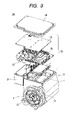
- FIG. 8 is a view showing the appearance of the motor integrated control unit mounting the power module in the first embodiment
- FIG. 9 is a view showing the disassembled motor integrated control unit.
- FIG. 10 is a general view showing manufacturing process of the power module in the first embodiment.
- FIG. 1 to FIG. 3 show an appropriate structure of the power module as an embodiment of the present invention.
- FIG. 1 is a whole perspective view of the present embodiment before mounting a power module 1 on the power module mounting portion 3 .
- FIG. 2 is a back view of the power module 1 shown in FIG. 1 .
- FIG. 3 is a sectional view taken along line III-III in FIG. 2 after mounting the power module 1 on the power module mounting portion 3 .
- the power module 1 of the present embodiment has a laminated structure which comprises a plurality of switching elements 10 for driving and controlling a external motor (not shown), a wiring portion of current circuit mounting a plurality of switching elements 10 , an insulation layer 12 consisting of an insulation material, and a heat radiation layer 13 diffusing and radiating heat from a plurality of switching elements 10 .
- the switching element 10 is a power semi-conductor element such as MOSFET or IGBT or the like. Also, the switching element 10 is a bear chip on which a silicon chip is mounted with exposed condition.
- An electrode pad is disposed at both ends of upper surface and reverse side surface of the switching element 10 .
- the electrode pad of the reverse side surface and the wiring portion for current circuit 11 are connected each other using a lead free solder 16 b .
- Such chip structure is capable of decreasing mounting area of the switching element 10 and size of the power module 1 .
- an electrode pad of the reverse side surface of the switching element 10 is connected to the wiring portion for current circuit 11 by lead free solder with high thermal conductivity and superior environment performance.
- both of the electrode pads of the upper surface and the wiring portion for current circuit 11 are connected with lead free solder 16 a through conductive stripe shaped bridge member 15 .
- the conductive stripe shaped bridge member 15 is made of cupper alloy material. It is preferable to use as the cupper alloy material, for example, tough pitch copper material and oxygen free cupper material with high thermal conductivity, low thermal expansion coefficient and low electric resistance coefficient. However, without limiting these materials, it is able to use cupper-molybdenum alloy material, cupper-tungsten alloy material or the like in comparison with the other metal material having a very low thermal expansion coefficient.
- At least a portion of electrical pads on the surface of the switching elements 10 uses lead free solder with high thermal conductivity and well environment performance and is connected to the wiring portion for current circuit 11 through the conductive stripe shaped bridge member 15 . As a result, it is able to diffuse heat of the switching element 10 from the upper surface of the switching element 10 effectively to the reverse side surface of the power module 1 .
- the wiring portion for current circuit 11 consists of a material having high thermal conductivity and low electric resistance such as cupper alloy or the like.
- the wiring thickness of the wiring portion for current circuit 11 is over 100 ⁇ m, preferable to 100 ⁇ m-175 ⁇ m.
- Such structure is capable of diffusing and radiating effectively heat of the switching element 10 to the reverse side surface of the power module 1 . Also, it is able to prevent heating of the wiring itself when flowing large current.
- Material having high thermal conductivity and well electric insulation is used as the insulation layer 12 .
- the insulation layer 12 Material having high thermal conductivity and well electric insulation is used.
- aluminum oxide material, silicon nitride material, aluminum nitride material, or alumna powder inserted epoxy resin material having high thermal conductivity, or the like are used.
- Using material having the high thermal conductivity and a well electric insulation is capable of insuring electric insulation performance between the wiring portion for current circuit 11 and the heat radiation layer 13 , and diffuse and radiate heat from the switching elements 10 to the reverse side surface of the power module 1 efficiently.
- the radiation layer 13 for example, it is preferable to use a material having high thermal conductivity and low thermal expansion coefficient comparing with other metal material, such as tough pitch cupper material and oxygen free cupper material.
- other metal material such as tough pitch cupper material and oxygen free cupper material.
- it is able to use aluminum alloy and light specific gravity or cupper-molybdenum alloy material having very low thermal expansion coefficient performance, cupper-tungsten alloy material, or alumna silicon carbide having high thermal conductivity comparing with other materials. Adopting such materials with high thermal conductivity is capable of diffusing and radiating the heat from the switching element more efficiently to the power module reverse side surface.
- FIG. 4 is a view showing a power module structure of the power module 1 of the present embodiment before the resin sealing process.
- a current sensing resistance element 18 and a temperature sensing element 19 are mounted on the wiring portion for current circuit 11 of the power module 1 . Including these elements, a control circuit for driving motor is constituted.
- FIG. 5 shows the other power module structure of the power module 1 of the present embodiment in the previous step of the resin sealing.
- a micro-computer 22 for controlling and supervising the switching elements 10 and an element 23 instituting a power source circuit are mounted on the wiring portion of current circuit 11 of the power module 1 .
- a circuit structure integrating a power circuit and control circuit may be adopted.
- the reverse side surface of the heat radiation layer 13 has a structure in which a portion except both ends of the longer sides is exposed to outside.
- the reverse side surface of resin 2 and the reverse side surface of the heat radiation layer 13 form a structure having a plane with height different from each other in the power module 1 .
- An exposure portion of the radiation layer 13 disposed on the reverse side surface of the power module, or a portion sealed with thin resin 2 is preferable to be formed to arrange the switching elements 10 at its center portion.
- Such structure may arrange the exposure portion or a portion with the thin resin seal so as to position the switching elements 10 in the minimum range as center. As a result, it is able to suppress efficiently the warp of all power modules 1 and to improve reliability to insure efficiently the radiation path.
- a structure sealed with thinner resin may be adopted instead of the exposed portion to the central portion of reverse side surface of the heat radiation layer 13 disposed at the reverse side surface of the power module 1 .
- a structure sealed with thinner resin may be adopted instead of the exposed portion to the central portion of reverse side surface of the heat radiation layer 13 disposed at the reverse side surface of the power module 1 .
- Such structure is able to obtain same effect as that above described.
- the structure that reverse side surface of the radiation layer 13 is sealed enable to improve the anti-corrosion performance of the heat radiation layer 13 in comparison with the structure that the reverse side surface is exposed.
- a salient 4 is provided with the power module mounting portion 3 for mounting the power module coinciding with the exposure shape of the heat radiation layer 13 of the power module 1 .
- the reverse side surface of radiation layer 13 of power module 1 is adhered to the salient 4 of the power module mounting portion 3 through grease 17 .
- the power module mounting portion 3 is preferable to be formed with a metal or the like having well heat radiating performance.
- an accommodating portion 5 to accommodate the sealing resin 2 which seals an end surface of the longer sides of the heat radiation layer 13 of the power module 1 is placed at the power module mounting portion 3 .
- the resin 2 is projected from the plane of the heat radiation layer 13 in the reverse side surface of the power module 1 . Therefore, the accommodation portion 5 disposed at the power module mounting portion 3 is so structured as to accommodate the salient portion projected from the heat radiation layer 13 in the resin 2 of the power module 1 .
- a plurality of the external terminals 20 of cupper alloy products having a L-shaped section to drive and control the motor is provided with the power module 1 .
- the surface of the external terminal 20 is plated, for example, Sn plating or Sn—Bi plating considering solder wetting performance and connection strength.
- an external terminal 20 a for conducting large current and an external terminal 20 b for transmitting signals are provided with a power module 1 as external terminals 20 .
- Large current for motor driving flows in the external terminal 20 a for conducting large current from the external power source through the switching elements 10 .
- a control signal to control ON/OFF for controlling current flowing through the motor is input to the external terminal 20 b for transmitting signal to transfer to control terminal switching element 10 . That is, the large current for driving motor flows based on the control signal input by external terminal 20 b for signal conducting through the external terminal for conducting large current 20 a.
- the external terminal 20 a for conducting large current As large current for motor driving flows through the external terminal 20 a for conducting large current, its width is selected to be larger than that of the external terminal 20 b of the signal transmitting.
- the external terminal 20 for conducting large current and the external terminal 20 b for transmitting signals may be set to same size and shape.
- an external terminals 20 a for conducting large current are disposed at both sides of the longer sides of power module 1 .
- an external terminal 20 b for transmitting signal is disposed at only one of the longer sides.
- the present invention is not limited to such structure and capable of changing appropriately considering influences of heat, noise and the like.
- Both of the external terminal 20 a for conducting large current and the external terminal 20 b for transmitting signal are connected each other using lead free solder to a connection portion 14 disposed on the wiring portion of current circuit 11 .
- lead free solder Sn—Cu solder, Sn—Ag—Cu solder, Sn—Ag—Cu—Bi solder, or the like are used, however, there is no necessary to limit to them.
- the external terminal 20 a for conducting large current and the external terminal 20 b for signal transmitting have a step portion 21 at a connection portion 14 .
- step portion 21 distance between the insulation layer 12 and the external terminal 20 becomes large in a portion except connection portion 14 .
- the salient 4 is provided with the power module mounting portion 3 coinciding with the exposed shape of the radiation layer 13 exposed to the reverse side surface of power module 1 .
- the power module 1 makes surface contact through the grease 17 having high thermal conductivity and is fixed to the power module mounting portion 3 .
- Such structure is capable of insuring radiation path from the reverse side surface of the power module 1 to the module mounting portion 3 .
- a high thermal conductivity radiation sheet and silicon adhesion agents may be used instead of the grease 17 .
- FIG. 6 shows the power module of the second embodiment in accordance with the present invention.
- the power module 1 of the present embodiment all of the both ends of the longer sides and both ends of the shorter sides of the heat radiation layer 13 are sealed by the resin 2 in reverse side surface of the heat radiation layer 13 .
- the resin 2 In the structure of the first embodiment, only both ends of the longer sides of the heat radiation layer 13 are sealed with the resin 2 .
- both ends of the longer sides and both ends of the shorter sides that is, by sealing all of four sides with the resin 2 , it is capable of keeping the heat radiation path and preventing warps of all the power modules 1 efficiently. As a result, provision of the power module with more improved reliability may be possible.
- FIG. 7 shows a power module of the third embodiment in accordance with of the present invention.
- the switching element 10 is mounted on upper portion of exposure region of the heat radiation layer 13 . Therefore, the resin 2 of the central portion is preferable to seal so as to avoid the mounting region of the switching elements 10 .
- FIG. 8 is an appearance view of a motor integrated control unit mounting the power module 1 in the present embodiment and FIG. 9 is a disassembling view of the motor integrated control unit of FIG. 8 .
- the motor integrated control unit 30 is used, for example, as a control system of an electric power steering.
- the motor integrated control unit 30 mainly comprises a motor 31 , a motor control unit 33 for driving and controlling the motor 31 , a housing 37 accommodating these and a cover 39 closing an opening of the housing 37 .
- a motor shaft 32 (rotating shaft) is projected from the motor 31 , and a back-up flange portion 38 is fixed around the motor shaft 32 .
- the motor control unit 33 is disposed in the housing 37 parallel to the motor shaft 32 of the motor 31 (around rotating shaft).
- the motor control unit 33 comprises a resin circuit board 34 mounting a micro-computer for controlling driving power of the motor 31 , a bus bar wiring board 35 having a path for supplying large current to the motor 3 , the power module 1 for flowing the large current to drive the motor 31 based on the control signal from a resin circuit board 34 , and a passive parts 36 including power module 1 flowing large current, power source relay, motor relay, coil, capacitor and the like.
- the resin circuit board 34 , bus bar wiring board 35 and the power module 1 are aligned in order from the opening in the housing 37 towards its bottom.
- the power module 1 is mounted on the power module mounting portion 3 positioned at the upper portion of the motor 31 .
- the external terminal 20 a for conducting large current of the power module 1 is connected to the bus bar wiring board 35 provided at the upper portion of the power module 1 .
- An external terminal 20 b for conducting signal of power module 1 is connected to the resin circuit board 34 provided at the upper portion of the bus bar wiring board 35 .
- the power module 1 is mounted on the power module mounting portion 3 close to the motor 31 of housing 37 and the power module mounting portion 3 is disposed as a portion of the housing 37 .
- the power module 1 is covered with the resin 2 and has a plurality of switching elements 10 for driving the motor 31 inside the resin.
- the plurality of switching elements 10 are disposed on the radiation layer 13 though an insulation layer 12 and the radiation layer 13 has an exposure region exposed to outside and a non-exposure region covered with the resin 2 .
- the heat radiation layer 13 is connected to the power module mounting portion 3 in the exposure region.
- the non-exposure region covered with the resin 2 is placed at the end of the heat radiation layer 13 .
- a salient 4 is provided coinciding with the exposure shape of the radiation layer 13 of the reverse side surface of the power module 1 . Accordingly, it is able to diffusing and radiating heat of the switching element 10 to bottom of the housing 37 of the reverse side surface of the power module 1 with high efficiency.
- the power module 1 is positioned between the bus bar wiring board 35 and the motor 31 .
- a resin circuit board 34 on which a micro computer for generating a control signal is disposed at the upper portion of the power module 1 and the bus bar wiring board 35 .
- the power module 1 and the bus bar wiring board 35 are positioned between the motor 31 and the resin circuit board 34 .
- passive portions 36 have a large capacitor, coil or the like to smooth voltage variation and form a voltage rising circuit. Therefore, by placing the passive parts 36 near the bus bar wiring board 35 , miniaturization of the motor integrated control unit 30 is realized.
- FIG. 10 is a general view showing manufacturing process of the power module in the present embodiment.
- the power module 1 is made through the manufacturing processes shown in [I]-[VII].
- lead free solder paste is printed on a metal board which the wiring portion for current 11 comprising a cupper alloy material of wiring thickness of 175 ⁇ m, an insulation layer 12 comprising an epoxy resin material and a radiation layer 13 composed of a tough pitch cupper are laminated.
- An external terminal 20 with a terminal frame 40 manufactured beforehand by press working of a cupper alloy plate mounting a sub-module mounting having a semi-conductor element such as a plurality of switching element 10 , a current sensing resistance element 18 , a temperature sensing element 19 and the like is mounted on solder paste of a wiring portion for current circuit.
- a step portion 21 is made at the press working beforehand.
- the sub-module 41 of previous process is set in a die of an injection-molding machine and the sub-module 41 is sealed with the resin 2 of epoxy thermo-setting type and taken out of the die.
- the present embodiment not only the upper surface and side surface of the power module 1 where a plurality of the switching elements are mounted but also at least a part of the heat radiation layer 13 placed at the reverse side surface of the power module 1 is exposed or sealed partially with thin resin, and sealed with the hardening type resin 2 so as to be plane different from the reverse side surface of the power module 1 in height.
- Such structure may decrease the difference of quantity of expansion and shrinking of the resin disposed on upper and lower surfaces of the power module 1 , as a result, it is able to suppress entire warp of the power module due to hardening and shrinking by resin hardening during manufacturing of the power module 1 , resin shrinking at cooling and expansion and shrinking at ambient temperature in the practical use. As a result, it is able to keep the heat radiation path and provide a power module 1 with high reliability.
- the structure which all of both ends of the longer sides of reverse side surface of the power module 1 are covered with the resin 2 is able to adopt a structure in which a portion of both ends of the longer sides is exposed and partially covered with the resin 2 .
- This may be applicable to the second and third embodiments as same way. If a portion of the reverse side surface of the radiation layer 13 is exposed so as to keep the heat radiation path, there is no limiting the shape of the sealing resin 2 .
- the embodiments in accordance with the present invention are explained as an assumption that the switching elements 10 be a bear chip. Instead, it is able to mount the switching elements sealed with resin beforehand.
Abstract
Description
Claims (16)
Applications Claiming Priority (2)
| Application Number | Priority Date | Filing Date | Title |
|---|---|---|---|
| JP2006-302243 | 2006-11-08 | ||
| JP2006302243A JP2008118067A (en) | 2006-11-08 | 2006-11-08 | Power module and motor-integrated controlling device |
Publications (2)
| Publication Number | Publication Date |
|---|---|
| US20080106160A1 US20080106160A1 (en) | 2008-05-08 |
| US7679182B2 true US7679182B2 (en) | 2010-03-16 |
Family
ID=39047643
Family Applications (1)
| Application Number | Title | Priority Date | Filing Date |
|---|---|---|---|
| US11/936,158 Expired - Fee Related US7679182B2 (en) | 2006-11-08 | 2007-11-07 | Power module and motor integrated control unit |
Country Status (3)
| Country | Link |
|---|---|
| US (1) | US7679182B2 (en) |
| EP (1) | EP1921911A1 (en) |
| JP (1) | JP2008118067A (en) |
Cited By (3)
| Publication number | Priority date | Publication date | Assignee | Title |
|---|---|---|---|---|
| US20090201651A1 (en) * | 2006-05-30 | 2009-08-13 | Shuichi Muramatsu | Resin sealing semiconductor device and electronic device using resin sealing semiconductor device |
| US20090224398A1 (en) * | 2008-03-04 | 2009-09-10 | Denso Corporation | Semiconductor module and method of manufacturing the same |
| US20180233437A1 (en) * | 2016-03-11 | 2018-08-16 | Shindengen Electric Manufacturing Co., Ltd. | Semiconductor device |
Families Citing this family (18)
| Publication number | Priority date | Publication date | Assignee | Title |
|---|---|---|---|---|
| JP5435284B2 (en) * | 2009-06-24 | 2014-03-05 | 株式会社デンソー | Drive device |
| DE102010017522A1 (en) * | 2009-06-24 | 2011-02-03 | ASMO Co., Ltd., Kosai-city | Drive device and semiconductor module |
| JP5516066B2 (en) | 2009-06-24 | 2014-06-11 | 株式会社デンソー | Drive device |
| JP5435286B2 (en) | 2009-06-24 | 2014-03-05 | 株式会社デンソー | Drive device |
| JP5435285B2 (en) | 2009-06-24 | 2014-03-05 | 株式会社デンソー | Drive device |
| JP5403073B2 (en) * | 2010-01-29 | 2014-01-29 | 株式会社村田製作所 | Power receiving device and power transmitting device |
| JP5380376B2 (en) * | 2010-06-21 | 2014-01-08 | 日立オートモティブシステムズ株式会社 | Power semiconductor device |
| JP5496357B2 (en) * | 2010-10-27 | 2014-05-21 | 三菱電機株式会社 | Motor drive control device for electric power steering |
| US9129949B2 (en) | 2011-02-09 | 2015-09-08 | Mitsubishi Electric Corporation | Power semiconductor module |
| JP5936310B2 (en) * | 2011-03-17 | 2016-06-22 | 三菱電機株式会社 | Power semiconductor module and its mounting structure |
| US8466541B2 (en) * | 2011-10-31 | 2013-06-18 | Infineon Technologies Ag | Low inductance power module |
| US10136555B2 (en) | 2013-05-21 | 2018-11-20 | Hitachi Automotive Systems, Ltd. | Power conversion apparatus having a metal plate for heat dissipation |
| CN105359262B (en) * | 2013-07-04 | 2019-02-19 | 三菱电机株式会社 | The manufacturing method of semiconductor device, semiconductor device |
| KR20240046638A (en) * | 2014-01-21 | 2024-04-09 | 퍼시몬 테크놀로지스 코포레이션 | Substrate transport vacuum platform |
| JP6470938B2 (en) * | 2014-10-06 | 2019-02-13 | 日立オートモティブシステムズ株式会社 | Power module and power converter |
| US10461010B2 (en) | 2016-04-04 | 2019-10-29 | Mitsubishi Electric Corporation | Power module, power semiconductor device and power module manufacturing method |
| WO2020144814A1 (en) * | 2019-01-10 | 2020-07-16 | 三菱電機株式会社 | Semiconductor device |
| FR3115947A1 (en) * | 2020-11-03 | 2022-05-06 | Valeo Equipements Electriques Moteur | ELECTRONIC MODULE FOR ELECTRIC MACHINE |
Citations (19)
| Publication number | Priority date | Publication date | Assignee | Title |
|---|---|---|---|---|
| US5440169A (en) | 1993-01-08 | 1995-08-08 | Mitsubishi Denki Kabushiki Kaisha | Resin-packaged semiconductor device with flow prevention dimples |
| US5469131A (en) * | 1992-08-28 | 1995-11-21 | Sanyo Electric Co., Ltd. | Hybrid integrated circuit device |
| US5559374A (en) * | 1993-03-25 | 1996-09-24 | Sanyo Electric Co., Ltd. | Hybrid integrated circuit |
| US5641944A (en) * | 1995-09-29 | 1997-06-24 | Allen-Bradley Company, Inc. | Power substrate with improved thermal characteristics |
| JPH09260550A (en) | 1996-03-22 | 1997-10-03 | Mitsubishi Electric Corp | Semiconductor device |
| US5703399A (en) * | 1995-11-15 | 1997-12-30 | Mitsubishi Denki Kabushiki Kaisha | Semiconductor power module |
| US5747875A (en) * | 1993-09-08 | 1998-05-05 | Mitsubishi Denki Kabushiki Kaisha | Semiconductor power module with high speed operation and miniaturization |
| US5920119A (en) * | 1996-02-22 | 1999-07-06 | Hitachi, Ltd. | Power semiconductor module employing metal based molded case and screw fastening type terminals for high reliability |
| US5942797A (en) * | 1996-04-02 | 1999-08-24 | Fuji Electric Co. Ltd. | Power semiconductor module |
| JP2001189325A (en) | 1999-12-28 | 2001-07-10 | Hitachi Ltd | Power module |
| JP2003031765A (en) | 2001-07-17 | 2003-01-31 | Hitachi Ltd | Power module and inverter |
| US6970367B2 (en) * | 2003-08-20 | 2005-11-29 | Matsushita Electric Industrial Co., Ltd. | Switching power supply |
| US7035106B2 (en) * | 2002-11-14 | 2006-04-25 | Samsung Electronics Co., Ltd. | Heat dissipation system for semiconductor device |
| US20060097380A1 (en) * | 2004-02-03 | 2006-05-11 | Kabushiki Kaisha Toshiba | Semiconductor module |
| US7242582B2 (en) * | 2004-04-20 | 2007-07-10 | Denso Corporation | Semiconductor module mounting structure, a cardlike semiconductor module, and heat receiving members bonded to the cardlike semiconductor module |
| US20070257343A1 (en) * | 2006-05-05 | 2007-11-08 | Hauenstein Henning M | Die-on-leadframe (dol) with high voltage isolation |
| US20070257568A1 (en) * | 2005-01-28 | 2007-11-08 | Mitsubishi Electric Corporation | Electric Rotating Machine |
| US20080007925A1 (en) * | 2006-07-10 | 2008-01-10 | Ibiden, Co., Ltd. | Package board integrated with power supply |
| US7445081B2 (en) * | 2006-04-21 | 2008-11-04 | Mitsubishi Electric Corporation | Electric power steering apparatus |
Family Cites Families (1)
| Publication number | Priority date | Publication date | Assignee | Title |
|---|---|---|---|---|
| JPH08298299A (en) * | 1995-04-27 | 1996-11-12 | Hitachi Ltd | Semiconductor device |
-
2006
- 2006-11-08 JP JP2006302243A patent/JP2008118067A/en active Pending
-
2007
- 2007-11-05 EP EP07021503A patent/EP1921911A1/en not_active Withdrawn
- 2007-11-07 US US11/936,158 patent/US7679182B2/en not_active Expired - Fee Related
Patent Citations (19)
| Publication number | Priority date | Publication date | Assignee | Title |
|---|---|---|---|---|
| US5469131A (en) * | 1992-08-28 | 1995-11-21 | Sanyo Electric Co., Ltd. | Hybrid integrated circuit device |
| US5440169A (en) | 1993-01-08 | 1995-08-08 | Mitsubishi Denki Kabushiki Kaisha | Resin-packaged semiconductor device with flow prevention dimples |
| US5559374A (en) * | 1993-03-25 | 1996-09-24 | Sanyo Electric Co., Ltd. | Hybrid integrated circuit |
| US5747875A (en) * | 1993-09-08 | 1998-05-05 | Mitsubishi Denki Kabushiki Kaisha | Semiconductor power module with high speed operation and miniaturization |
| US5641944A (en) * | 1995-09-29 | 1997-06-24 | Allen-Bradley Company, Inc. | Power substrate with improved thermal characteristics |
| US5703399A (en) * | 1995-11-15 | 1997-12-30 | Mitsubishi Denki Kabushiki Kaisha | Semiconductor power module |
| US5920119A (en) * | 1996-02-22 | 1999-07-06 | Hitachi, Ltd. | Power semiconductor module employing metal based molded case and screw fastening type terminals for high reliability |
| JPH09260550A (en) | 1996-03-22 | 1997-10-03 | Mitsubishi Electric Corp | Semiconductor device |
| US5942797A (en) * | 1996-04-02 | 1999-08-24 | Fuji Electric Co. Ltd. | Power semiconductor module |
| JP2001189325A (en) | 1999-12-28 | 2001-07-10 | Hitachi Ltd | Power module |
| JP2003031765A (en) | 2001-07-17 | 2003-01-31 | Hitachi Ltd | Power module and inverter |
| US7035106B2 (en) * | 2002-11-14 | 2006-04-25 | Samsung Electronics Co., Ltd. | Heat dissipation system for semiconductor device |
| US6970367B2 (en) * | 2003-08-20 | 2005-11-29 | Matsushita Electric Industrial Co., Ltd. | Switching power supply |
| US20060097380A1 (en) * | 2004-02-03 | 2006-05-11 | Kabushiki Kaisha Toshiba | Semiconductor module |
| US7242582B2 (en) * | 2004-04-20 | 2007-07-10 | Denso Corporation | Semiconductor module mounting structure, a cardlike semiconductor module, and heat receiving members bonded to the cardlike semiconductor module |
| US20070257568A1 (en) * | 2005-01-28 | 2007-11-08 | Mitsubishi Electric Corporation | Electric Rotating Machine |
| US7445081B2 (en) * | 2006-04-21 | 2008-11-04 | Mitsubishi Electric Corporation | Electric power steering apparatus |
| US20070257343A1 (en) * | 2006-05-05 | 2007-11-08 | Hauenstein Henning M | Die-on-leadframe (dol) with high voltage isolation |
| US20080007925A1 (en) * | 2006-07-10 | 2008-01-10 | Ibiden, Co., Ltd. | Package board integrated with power supply |
Non-Patent Citations (2)
| Title |
|---|
| European Search Report dated Mar. 10, 2008 Seven (7) pages. |
| Japanese Office Action mailed May 12, 2009 and an English translation thereof. |
Cited By (6)
| Publication number | Priority date | Publication date | Assignee | Title |
|---|---|---|---|---|
| US20090201651A1 (en) * | 2006-05-30 | 2009-08-13 | Shuichi Muramatsu | Resin sealing semiconductor device and electronic device using resin sealing semiconductor device |
| US7868451B2 (en) * | 2006-05-30 | 2011-01-11 | Kokusan Denki Co. Ltd. | Resin sealing semiconductor device and electronic device using resin sealing semiconductor device |
| US20090224398A1 (en) * | 2008-03-04 | 2009-09-10 | Denso Corporation | Semiconductor module and method of manufacturing the same |
| US7944045B2 (en) * | 2008-03-04 | 2011-05-17 | Denso Corporation | Semiconductor module molded by resin with heat radiation plate opened outside from mold |
| US20180233437A1 (en) * | 2016-03-11 | 2018-08-16 | Shindengen Electric Manufacturing Co., Ltd. | Semiconductor device |
| US10453781B2 (en) * | 2016-03-11 | 2019-10-22 | Shindengen Electric Manufacturing Co., Ltd. | Semiconductor device |
Also Published As
| Publication number | Publication date |
|---|---|
| US20080106160A1 (en) | 2008-05-08 |
| JP2008118067A (en) | 2008-05-22 |
| EP1921911A1 (en) | 2008-05-14 |
Similar Documents
| Publication | Publication Date | Title |
|---|---|---|
| US7679182B2 (en) | Power module and motor integrated control unit | |
| US6690087B2 (en) | Power semiconductor module ceramic substrate with upper and lower plates attached to a metal base | |
| US7687903B2 (en) | Power module and method of fabricating the same | |
| JP2021516869A (en) | Double-sided cooling type power module and its manufacturing method | |
| JP2007227957A (en) | Semiconductor device module | |
| WO2013088864A1 (en) | Semiconductor device | |
| CN111916411A (en) | Power module for the controlled supply of electrical power to consumers | |
| JP2009278134A (en) | Power module and inverter | |
| JP2010034350A (en) | Semiconductor device | |
| US10163752B2 (en) | Semiconductor device | |
| KR101828189B1 (en) | Circuit board assembly, control device for a cooler fan module and method | |
| JP4403166B2 (en) | Power module and power converter | |
| JP2006287168A (en) | Package structure equipped with hybrid circuit and composite substrate | |
| JP6948855B2 (en) | Power semiconductor device and power conversion device using it | |
| KR20180087330A (en) | Metal slug for double sided cooling of power module | |
| KR20150071336A (en) | Power module Package and Manufacturing Method for the same | |
| JP7018756B2 (en) | Power module board and power module | |
| US20240006280A1 (en) | Intelligent power module and manufacturing method thereof | |
| JP5558405B2 (en) | Semiconductor device | |
| JP5195828B2 (en) | Semiconductor device | |
| US20220418088A1 (en) | Power module with housed power semiconductors for controllable electrical power supply of a consumer, and method for producing same | |
| JP2002314037A (en) | Power semiconductor module | |
| US20230027138A1 (en) | Power module | |
| US20230096381A1 (en) | Semiconductor device and method for manufacturing semiconductor device | |
| US20220295662A1 (en) | Power electronics module with improved cooling |
Legal Events
| Date | Code | Title | Description |
|---|---|---|---|
| AS | Assignment |
Owner name: HITACHI, LTD., JAPAN Free format text: ASSIGNMENT OF ASSIGNORS INTEREST;ASSIGNORS:YOSHINARI, HIDETO;KANEKO, YUJIRO;HARADA, MASAHIDE;AND OTHERS;REEL/FRAME:020379/0116;SIGNING DATES FROM 20071029 TO 20071030 Owner name: HITACHI, LTD.,JAPAN Free format text: ASSIGNMENT OF ASSIGNORS INTEREST;ASSIGNORS:YOSHINARI, HIDETO;KANEKO, YUJIRO;HARADA, MASAHIDE;AND OTHERS;SIGNING DATES FROM 20071029 TO 20071030;REEL/FRAME:020379/0116 |
|
| FEPP | Fee payment procedure |
Free format text: PAYOR NUMBER ASSIGNED (ORIGINAL EVENT CODE: ASPN); ENTITY STATUS OF PATENT OWNER: LARGE ENTITY |
|
| FPAY | Fee payment |
Year of fee payment: 4 |
|
| FEPP | Fee payment procedure |
Free format text: MAINTENANCE FEE REMINDER MAILED (ORIGINAL EVENT CODE: REM.) |
|
| LAPS | Lapse for failure to pay maintenance fees |
Free format text: PATENT EXPIRED FOR FAILURE TO PAY MAINTENANCE FEES (ORIGINAL EVENT CODE: EXP.) |
|
| STCH | Information on status: patent discontinuation |
Free format text: PATENT EXPIRED DUE TO NONPAYMENT OF MAINTENANCE FEES UNDER 37 CFR 1.362 |
|
| FP | Lapsed due to failure to pay maintenance fee |
Effective date: 20180316 |