US7691663B2 - CMOS image sensor having double gate insulator therein and method for manufacturing the same - Google Patents
CMOS image sensor having double gate insulator therein and method for manufacturing the same Download PDFInfo
- Publication number
- US7691663B2 US7691663B2 US11/657,908 US65790807A US7691663B2 US 7691663 B2 US7691663 B2 US 7691663B2 US 65790807 A US65790807 A US 65790807A US 7691663 B2 US7691663 B2 US 7691663B2
- Authority
- US
- United States
- Prior art keywords
- area
- pixel array
- mosfet
- logic circuit
- insulating layer
- Prior art date
- Legal status (The legal status is an assumption and is not a legal conclusion. Google has not performed a legal analysis and makes no representation as to the accuracy of the status listed.)
- Expired - Fee Related, expires
Links
- 239000012212 insulator Substances 0.000 title claims abstract description 64
- 238000000034 method Methods 0.000 title claims abstract description 60
- 238000004519 manufacturing process Methods 0.000 title claims abstract description 19
- 239000004065 semiconductor Substances 0.000 claims abstract description 38
- 239000000758 substrate Substances 0.000 claims abstract description 30
- 238000012546 transfer Methods 0.000 claims description 13
- KRHYYFGTRYWZRS-UHFFFAOYSA-N Fluorane Chemical compound F KRHYYFGTRYWZRS-UHFFFAOYSA-N 0.000 claims description 9
- QAOWNCQODCNURD-UHFFFAOYSA-N Sulfuric acid Chemical compound OS(O)(=O)=O QAOWNCQODCNURD-UHFFFAOYSA-N 0.000 claims description 9
- 230000000295 complement effect Effects 0.000 claims description 9
- 229910044991 metal oxide Inorganic materials 0.000 claims description 9
- 150000004706 metal oxides Chemical class 0.000 claims description 9
- VYPSYNLAJGMNEJ-UHFFFAOYSA-N Silicium dioxide Chemical compound O=[Si]=O VYPSYNLAJGMNEJ-UHFFFAOYSA-N 0.000 claims description 6
- 229910052814 silicon oxide Inorganic materials 0.000 claims description 6
- 238000001039 wet etching Methods 0.000 claims description 4
- QPJSUIGXIBEQAC-UHFFFAOYSA-N n-(2,4-dichloro-5-propan-2-yloxyphenyl)acetamide Chemical compound CC(C)OC1=CC(NC(C)=O)=C(Cl)C=C1Cl QPJSUIGXIBEQAC-UHFFFAOYSA-N 0.000 claims description 3
- 230000001590 oxidative effect Effects 0.000 claims description 3
- 238000000151 deposition Methods 0.000 claims 6
- 230000008021 deposition Effects 0.000 claims 3
- 238000005137 deposition process Methods 0.000 claims 1
- 239000010410 layer Substances 0.000 description 32
- 238000009792 diffusion process Methods 0.000 description 16
- 208000022010 Lhermitte-Duclos disease Diseases 0.000 description 6
- 230000003287 optical effect Effects 0.000 description 4
- 206010034972 Photosensitivity reaction Diseases 0.000 description 3
- 238000005516 engineering process Methods 0.000 description 3
- 238000005468 ion implantation Methods 0.000 description 3
- 230000036211 photosensitivity Effects 0.000 description 3
- 238000012545 processing Methods 0.000 description 3
- 239000002356 single layer Substances 0.000 description 3
- 239000003990 capacitor Substances 0.000 description 2
- 238000005530 etching Methods 0.000 description 2
- 230000005669 field effect Effects 0.000 description 2
- 238000002955 isolation Methods 0.000 description 2
- 229920006395 saturated elastomer Polymers 0.000 description 2
- 229910052710 silicon Inorganic materials 0.000 description 2
- 239000010703 silicon Substances 0.000 description 2
- QVGXLLKOCUKJST-UHFFFAOYSA-N atomic oxygen Chemical compound [O] QVGXLLKOCUKJST-UHFFFAOYSA-N 0.000 description 1
- 238000006243 chemical reaction Methods 0.000 description 1
- 238000011161 development Methods 0.000 description 1
- 238000001312 dry etching Methods 0.000 description 1
- 230000005684 electric field Effects 0.000 description 1
- 238000012986 modification Methods 0.000 description 1
- 230000004048 modification Effects 0.000 description 1
- 229910052760 oxygen Inorganic materials 0.000 description 1
- 239000001301 oxygen Substances 0.000 description 1
- 125000006850 spacer group Chemical group 0.000 description 1
Images


Classifications
-
- H—ELECTRICITY
- H01—ELECTRIC ELEMENTS
- H01L—SEMICONDUCTOR DEVICES NOT COVERED BY CLASS H10
- H01L27/00—Devices consisting of a plurality of semiconductor or other solid-state components formed in or on a common substrate
- H01L27/14—Devices consisting of a plurality of semiconductor or other solid-state components formed in or on a common substrate including semiconductor components sensitive to infrared radiation, light, electromagnetic radiation of shorter wavelength or corpuscular radiation and specially adapted either for the conversion of the energy of such radiation into electrical energy or for the control of electrical energy by such radiation
- H01L27/144—Devices controlled by radiation
- H01L27/146—Imager structures
- H01L27/14683—Processes or apparatus peculiar to the manufacture or treatment of these devices or parts thereof
- H01L27/14689—MOS based technologies
-
- H—ELECTRICITY
- H01—ELECTRIC ELEMENTS
- H01L—SEMICONDUCTOR DEVICES NOT COVERED BY CLASS H10
- H01L27/00—Devices consisting of a plurality of semiconductor or other solid-state components formed in or on a common substrate
- H01L27/14—Devices consisting of a plurality of semiconductor or other solid-state components formed in or on a common substrate including semiconductor components sensitive to infrared radiation, light, electromagnetic radiation of shorter wavelength or corpuscular radiation and specially adapted either for the conversion of the energy of such radiation into electrical energy or for the control of electrical energy by such radiation
- H01L27/144—Devices controlled by radiation
- H01L27/146—Imager structures
- H01L27/14601—Structural or functional details thereof
- H01L27/14609—Pixel-elements with integrated switching, control, storage or amplification elements
Definitions
- the present invention relates to a method for manufacturing a semiconductor device; and, more particularly, to a method for manufacturing a complementary metal oxide semiconductor (CMOS) image sensor having a double gate insulator in a pixel array with enhanced optical property and electrical property.
- CMOS complementary metal oxide semiconductor
- a photodiode image sensor device is the most commonly used a device for detecting images.
- a typical photodiode image sensor device comprises a reset transistor and a light sensor region formed by a photodiode.
- a photodiode is formed with an n-type doped region and a p-type substrate.
- a voltage is applied to the reset transistor gate to turn on the reset transistor and to charge the N/P diode junction capacitor.
- the reset transistor is turned off when the charging of the N/P diode junction capacitor has reached a certain high voltage.
- the N/P diode generates a reverse bias to form a depletion region.
- a charge coupled device (CCD) image sensor has a high dynamic range and a low dark current.
- the sophistication of the current technology of the CCD image sensor allows the CCD image sensor to become the most popular image sensing device.
- the manufacturing for the CCD image sensor is, however, rather special.
- the price of the CCD image sensor is therefore very high.
- the driver requires a high voltage operation, leading to problems of high power dissipation and inability of random access of memory.
- CMOS complementary metal oxide semiconductor
- SOC system on a chip
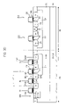
- FIG. 1 there is provided a cross sectional view of a conventional CMOS image sensor 100 including a semiconductor substrate 110 , a p-type epitaxial layer 112 , a pixel array 101 , a logic circuit 102 and field oxide (FOX) regions.
- the p-type epitaxial layer 112 is formed by epitaxially growing up an upper portion of the p-type semiconductor substrate 110 .
- the pixel array 101 and the logic circuit 102 are isolated from each other by forming the FOX region therebetween.
- a p-well 114 is formed in a predetermined location of the p-type epitaxial layer 112 of the pixel array 101 , where a drive transistor (Dx) and a select transistor (Sx) are formed in a post fabrication process.
- a drive transistor (Dx) and a select transistor (Sx) are formed in a post fabrication process.
- a buried photodiode (BPD) In the other predetermined location of the p-type epitaxial layer 112 in the pixel array 101 , there is formed a buried photodiode (BPD), where a transfer transistor (Tx) and a reset transistor (Rx) are formed by a post fabrication process.
- BPD buried photodiode
- the BPD has a PN junction of a deep n-type diffusion layer (DEEP N ⁇ ) and a shallow p-type diffusion layer (P 0 ), wherein the p-type diffusion layer (P 0 ) is formed on the deep n-type diffusion layer (DEEP N ⁇ ) by using a method such as an ion-implantation technique or the like.
- DEEP N ⁇ deep n-type diffusion layer
- P 0 shallow p-type diffusion layer
- One side of a gate electrode 116 A of the transfer transistor (Tx) is connected to the BPD and the other side is connected to a floating diffusion region (FD), wherein the gate electrode 116 A of the transfer transistor (Tx) is formed on a gate insulator 134 .
- a gate electrode 116 B of the reset transistor (Rx) is connected to the floating diffusion region (FD) and the other is connected to a power supply voltage (VDD), wherein the gate electrode 116 B of the reset transistor (Rx) is formed on the gate insulator 134 .
- the drive transistor (Dx) and the select transistor (Sx) have each n-type lightly doped drains (N-LDD) 118 in source/drain regions 120 by ion-implanting p-type atoms into the p-well 114 , while the reset transistor (Rx) and transfer transistor (Tx) have no N-LDDs therebetween.
- One of the source/drain regions 120 of the select transistor (Sx) plays a role as an output.
- a gate electrode 116 C of the drive transistor (Dx) is connected to the floating diffusion region (FD).
- each gate insulator 134 employs a single layer in the conventional CMOS image sensor.
- a reference numeral 138 which is not illustrated above is sidewall spacers.
- a p-well 122 for forming an n-MOSFET (n-type metal-oxide-silicon field effect transistor) 150 and an n-well 124 for forming a p-MOSFET 152 , wherein the p-well 122 and the n-well 124 are disposed side by side in the p-type epitaxial layer 112 .
- n-MOSFET n-type metal-oxide-silicon field effect transistor
- the n-MOSFET 150 has source/drain regions 126 with N-LDDs 128 by ion-implanting p-type atoms into the p-well 122 and the p-MOSFET 152 has source/drain regions 130 with P-LDDs 132 by ion-implanting n-type atoms into the n-well 124 .
- the conventional CMOS image sensor 100 having the single gate insulator 134 in the pixel array 101 may be applicable to device scale beyond 0.35 ⁇ m without lowering a photosensitivity and an electrical property.
- the conventional CMOS image sensor 100 has the single gate insulator 134 in both the pixel array 101 and the logic circuit 102 so that it is very difficult to secure desired optical property such as photosensitivity and electrical property simultaneously, the conventional CMOS image sensor 100 can be hardly applicable to the device scale less than 0.25 ⁇ m using a deep submicron technology.
- CMOS complementary metal oxide semiconductor
- CMOS complementary metal oxide semiconductor
- a semiconductor substrate incorporating therein a p-type epitaxial layer formed by epitaxially growing up an upper portion of the semiconductor substrate; a pixel array formed in one predetermined location of a semiconductor substrate, having a plurality of transistors and active areas therein; and a logic circuit formed in the other predetermined location of the semiconductor substrate having active areas and at least one transistor for processing a signal from the pixel array, wherein a gate insulator of each transistor in the pixel array is thicker than a gate insulator of the transistor in the logic circuit.
- CMOS complementary metal oxide semiconductor
- a method for manufacturing a CMOS image sensor including the steps of: a) preparing a semiconductor substrate incorporating therein a p-type epitaxial layer, wherein the semiconductor substrate is divided into two parts of which one part is defined as a pixel array and the other part is defined as a logic circuit, the pixel array being isolated from the logic circuit by means of a field oxide region therebetween; b) forming a first gate insulator on a top face of the p-type epitaxial layer; c) forming a mask on a top face of the first gate insulator in the pixel array; d) removing the first gate insulator in the logic circuit by using the mask; e) removing the mask in the pixel array; f) forming the second gate insulator on the top face of the first gate insulator in the pixel array and a top face of the p-type epitaxial layer in the logic circuit; g) forming a photo
- FIG. 1 is a cross sectional view setting forth a conventional complementary metal oxide semiconductor (CMOS) image sensor having a single gate insulator in a pixel array;
- CMOS complementary metal oxide semiconductor
- FIG. 2 is a cross sectional view setting forth a CMOS image sensor having a double gate insulator in a pixel array in accordance with a preferred embodiment of the present invention.
- FIGS. 3A to 3D are cross sectional views setting forth a method for manufacturing a CMOS image sensor having a double gate insulator in a pixel array in accordance with a preferred embodiment of the present invention.
- FIG. 2 and FIGS. 3A to 3D cross sectional views of a complementary metal oxide semiconductor (CMOS) image sensor and cross sectional views setting forth a method for the manufacture thereof in accordance with a preferred embodiment of the present invention. It should be noted that like parts appearing in FIG. 2 and FIGS. 3A to 3D are represented by like reference numerals.
- CMOS complementary metal oxide semiconductor
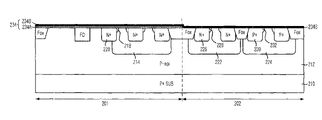
- CMOS image sensor 200 including a semiconductor substrate 210 , a p-type epitaxial layer 212 , a pixel array 201 , a logic circuit 202 and field oxide (FOX) regions.
- the p-type epitaxial layer 212 is formed by epitaxially growing up an upper portion of the p-type semiconductor substrate 210 .
- the pixel array 201 and the logic circuit 202 are isolated from each other by forming a FOX region of a shallow trench isolation (STI) therebetween. Additionally, another FOX region of the STI formed in the logic circuit isolates elements in the logic circuit from each other.
- STI shallow trench isolation
- a p-well 214 is formed in a predetermined location of the p-type epitaxial layer 212 in the pixel array 201 , where a drive transistor (Dx) and a select transistor (Sx) are formed in a post fabrication process.
- a drive transistor (Dx) and a select transistor (Sx) are formed in a post fabrication process.
- a buried photodiode (BPD) In the other predetermined location of the p-type epitaxial layer 212 in the pixel array, there is formed a buried photodiode (BPD), where a transfer transistor (Tx) and a reset transistor (Rx) are formed by a post fabrication process.
- the BPD has a PN junction of a deep n-type diffusion layer (DEEP N ⁇ ) and a shallow p-type diffusion layer (P 0 ), wherein the p-type diffusion layer (P 0 ) is formed on the deep n-type diffusion layer (DEEP N ⁇ ) by using a method such as an ion-implantation technique or the like.
- DEEP N ⁇ deep n-type diffusion layer
- P 0 shallow p-type diffusion layer
- One side of a gate electrode 216 A of the transfer transistor (Tx) is connected to the BPD and the other side is connected to a floating diffusion region (FD), wherein the gate electrode 216 A of the transfer transistor (Tx) is formed on a double gate insulator having a first and a second gate insulators 234 A, 234 B.
- a gate electrode 216 B of the reset transistor (Rx) is connected to the floating diffusion region (FD) and the other side is connected to a power supply voltage (VDD), wherein the gate electrode 216 B of the reset transistor (Rx) is also formed on the double gate insulator 234 .
- the drive transistor (Dx) and the select transistor (Sx) have each n-type lightly doped drains (N-LDD) 218 in source/drain regions 220 by ion-implanting p-type atoms into the p-well 214 , while the reset transistor (Rx) and transfer transistor (Tx) have no N-LDDs therein.
- One of the source/drain regions 220 of the select transistor (Sx) plays a role as an output.
- a gate electrode 216 C of the drive transistor (Dx) is connected to the floating diffusion region (FD).
- each transistor in the pixel array 201 has a gate structure of a double gate insulator 234 .
- the first gate insulator 234 A is formed on the p-type epitaxial layer 212 and the second gate insulator 234 B is formed on the first gate insulator 234 A.
- a thickness of the double gate insulator 234 is preferably in range of about 40 ⁇ to about 90 ⁇ .
- a p-well 222 for forming an n-MOSFET (n-type metal-oxide-silicon field effect transistor) 250 and an n-well 224 for forming a p-MOSFET 252 , wherein the p-well 222 and the n-well 224 are disposed side by side in the p-type epitaxial layer 212 .
- n-MOSFET n-type metal-oxide-silicon field effect transistor
- the n-MOSFET 250 has source/drain regions 226 with N-LDDs 228 by ion-implanting p-type atoms into the p-well 222 and the p-MOSFET 252 has source/drain regions 230 with P-LDDs 232 by ion-implanting n-type atoms into the n-well 224 .
- each transistor in the logic circuit 202 has a single gate insulator, i.e., the second gate insulator 234 B.
- the thickness of the single gate insulator is in the range of about 5 ⁇ to about 40 ⁇ .
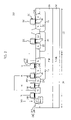
- FIGS. 3A to 3D there are shown cross sectional views setting forth a method for manufacturing a CMOS image sensor 200 in accordance with a preferred embodiment of the present invention.
- the inventive method for manufacturing the CMOS image sensor 200 begins with preparing a p-type semiconductor substrate 210 incorporating therein a p-type epitaxial layer 212 formed by epitaxially growing up an upper portion of the semiconductor substrate 210 , wherein the semiconductor substrate 210 is divided into two parts of which one is a pixel array 201 and the other is a logic circuit 202 .
- a field oxide (FOX) region is formed in a predetermined location of the p-type epitaxial layer 212 disposed between the pixel array 201 and the logic circuit 202 by using a method such as a shallow trench isolation (STI) process or the like, for isolating the pixel array from the logic circuit.
- a first p-well 214 is formed in the p-type epitaxial layer 212 of the pixel array 201 by using a method such as an ion-implantation process or the like.
- a second p-well 222 and an n-well 224 is formed in the logic circuit 202 .
- a first gate insulator 234 A is formed on a top face of the p-type epitaxial layer 212 , wherein the first gate insulator 234 A can employ silicon oxide (SiO 2 ) by thermally oxidizing the p-type epitaxial layer 212 .
- a mask layer e.g., a photosensitive film
- a mask layer is formed on a top face of the first gate insulator 234 A and is patterned into a predetermined configuration through a light exposure and a development processes, thereby forming a mask 235 formed only on the top face of the first gate insulator 234 A in the p-type epitaxial layer 212 of the pixel array 201 .
- the first gate insulator 234 A in the logic circuit 202 is wet-etched by using the mask 235 as an etch mask, whereby the first gate insulator 234 A remains only on the top face of the p-type epitaxial layer 212 of the pixel array 201 .
- a wet-etching process is carried out by using hydrofluoric acid (HF), buffered oxide etchant (BOE) or the like.
- the mask 235 is removed by means of a predetermined etching process such as a dry etching process making use of an oxygen (O 2 ) plasma, a wet etching process making use of a sulfuric acid (H 2 SO 4 ), an etching process making use of a thinner or the like.
- a second gate insulator 234 B is formed on the first gate insulator 234 A and the p-type epitaxial layer 212 of the logic circuit 202 .
- each transistor in the pixel array 201 has a thick double gate insulator 234 while each transistor in the logic circuit 202 has a single layer of the second gate insulator 234 B.
- a buried photodiode (BPD), a transfer transistor (Tx), a reset transistor (Rx), a drive transistor (Dx) and a select transistor (Sx) are formed in the pixel array 201 .
- an n-MOSFET 250 and a p-MOSFET 252 are formed in the logic circuit 202 . Therefore, an inventive CMOS image sensor 200 is achieved.
- the processes for fabricating above transistors and MOSFETs are well-known to those skilled in the art, so further explanation will be abbreviated in the present invention.
- the inventive CMOS image sensor 200 employs the double gate insulator 234 in the pixel array 201 compared with the conventional CMOS image sensor 100 employing a single gate insulator therein. Therefore, the inventive CMOS image sensor 200 has an advantage that it is possible to apply high operating voltage ranging from about 2.5 V to 3.3 V so as to secure sufficient saturated charges due to the thick double gate insulator 234 in the pixel array 201 . In addition, it is also possible to secure an appropriate dynamic range because of the sufficient saturated charges.
- the inventive CMOS image sensor 200 can be applicable to a portable manufactures such as a mobile phone, a digital camera or the like which requires high speed and high efficiency property.
Abstract
Description
Claims (18)
Priority Applications (3)
| Application Number | Priority Date | Filing Date | Title |
|---|---|---|---|
| US11/657,908 US7691663B2 (en) | 2003-04-30 | 2007-01-24 | CMOS image sensor having double gate insulator therein and method for manufacturing the same |
| US12/723,409 US8143626B2 (en) | 2003-04-30 | 2010-03-12 | CMOS image sensor having double gate insulator therein |
| US13/424,957 US8629023B2 (en) | 2003-04-30 | 2012-03-20 | CMOS image sensor having double gate insulator therein and method for manufacturing the same |
Applications Claiming Priority (4)
| Application Number | Priority Date | Filing Date | Title |
|---|---|---|---|
| KR2003-27810 | 2003-04-30 | ||
| KR10-2003-0027810A KR100523671B1 (en) | 2003-04-30 | 2003-04-30 | Cmos image sensor with double gateoxide and method of fabricating the same |
| US10/731,853 US20040217394A1 (en) | 2003-04-30 | 2003-12-08 | CMOS image sensor having double gate insulator therein and method for manufacturing the same |
| US11/657,908 US7691663B2 (en) | 2003-04-30 | 2007-01-24 | CMOS image sensor having double gate insulator therein and method for manufacturing the same |
Related Parent Applications (1)
| Application Number | Title | Priority Date | Filing Date |
|---|---|---|---|
| US10/731,853 Continuation-In-Part US20040217394A1 (en) | 2003-04-30 | 2003-12-08 | CMOS image sensor having double gate insulator therein and method for manufacturing the same |
Related Child Applications (1)
| Application Number | Title | Priority Date | Filing Date |
|---|---|---|---|
| US12/723,409 Continuation US8143626B2 (en) | 2003-04-30 | 2010-03-12 | CMOS image sensor having double gate insulator therein |
Publications (2)
| Publication Number | Publication Date |
|---|---|
| US20070120159A1 US20070120159A1 (en) | 2007-05-31 |
| US7691663B2 true US7691663B2 (en) | 2010-04-06 |
Family
ID=33308364
Family Applications (4)
| Application Number | Title | Priority Date | Filing Date |
|---|---|---|---|
| US10/731,853 Abandoned US20040217394A1 (en) | 2003-04-30 | 2003-12-08 | CMOS image sensor having double gate insulator therein and method for manufacturing the same |
| US11/657,908 Expired - Fee Related US7691663B2 (en) | 2003-04-30 | 2007-01-24 | CMOS image sensor having double gate insulator therein and method for manufacturing the same |
| US12/723,409 Expired - Lifetime US8143626B2 (en) | 2003-04-30 | 2010-03-12 | CMOS image sensor having double gate insulator therein |
| US13/424,957 Expired - Lifetime US8629023B2 (en) | 2003-04-30 | 2012-03-20 | CMOS image sensor having double gate insulator therein and method for manufacturing the same |
Family Applications Before (1)
| Application Number | Title | Priority Date | Filing Date |
|---|---|---|---|
| US10/731,853 Abandoned US20040217394A1 (en) | 2003-04-30 | 2003-12-08 | CMOS image sensor having double gate insulator therein and method for manufacturing the same |
Family Applications After (2)
| Application Number | Title | Priority Date | Filing Date |
|---|---|---|---|
| US12/723,409 Expired - Lifetime US8143626B2 (en) | 2003-04-30 | 2010-03-12 | CMOS image sensor having double gate insulator therein |
| US13/424,957 Expired - Lifetime US8629023B2 (en) | 2003-04-30 | 2012-03-20 | CMOS image sensor having double gate insulator therein and method for manufacturing the same |
Country Status (4)
| Country | Link |
|---|---|
| US (4) | US20040217394A1 (en) |
| JP (2) | JP4795642B2 (en) |
| KR (1) | KR100523671B1 (en) |
| TW (3) | TWI405329B (en) |
Cited By (3)
| Publication number | Priority date | Publication date | Assignee | Title |
|---|---|---|---|---|
| US20120295385A1 (en) * | 2008-11-19 | 2012-11-22 | Omnivision Technologies, Inc. | Lightly-doped drains (ldd) of image sensor transistors using selective epitaxy |
| US20170018430A1 (en) * | 2015-07-16 | 2017-01-19 | Silergy Semiconductor Technology (Hangzhou) Ltd | Semiconductor structure and manufacture method thereof |
| US9953876B1 (en) | 2016-09-30 | 2018-04-24 | Globalfoundries Inc. | Method of forming a semiconductor device structure and semiconductor device structure |
Families Citing this family (33)
| Publication number | Priority date | Publication date | Assignee | Title |
|---|---|---|---|---|
| WO2005109512A1 (en) * | 2004-05-06 | 2005-11-17 | Canon Kabushiki Kaisha | Photoelectric conversion device and manufacturing method thereof |
| US7115925B2 (en) * | 2005-01-14 | 2006-10-03 | Omnivision Technologies, Inc. | Image sensor and pixel having an optimized floating diffusion |
| JP4312162B2 (en) * | 2005-01-25 | 2009-08-12 | 富士通マイクロエレクトロニクス株式会社 | Manufacturing method of semiconductor device |
| JP2006253316A (en) * | 2005-03-09 | 2006-09-21 | Sony Corp | Solid-state image sensing device |
| EP1858082A4 (en) * | 2005-03-11 | 2011-01-19 | Fujitsu Semiconductor Ltd | Image sensor where photodiode region is embedded and its manufacturing method |
| KR100653716B1 (en) * | 2005-07-19 | 2006-12-05 | 삼성전자주식회사 | Image sensor and method of manufacturing the same |
| US20070045668A1 (en) * | 2005-08-26 | 2007-03-01 | Micron Technology, Inc. | Vertical anti-blooming control and cross-talk reduction for imagers |
| KR100714605B1 (en) * | 2005-08-31 | 2007-05-07 | 매그나칩 반도체 유한회사 | Method for fabrication of cmos image sensor |
| KR100722691B1 (en) * | 2005-11-07 | 2007-05-29 | 플래닛팔이 주식회사 | Unit pixel of Color CMOS image sensor |
| WO2007077286A1 (en) | 2006-01-05 | 2007-07-12 | Artto Aurola | Semiconductor radiation detector detecting visible light |
| JP2007317741A (en) * | 2006-05-23 | 2007-12-06 | Matsushita Electric Ind Co Ltd | Solid-state imaging device and manufacturing method therefor |
| KR100801447B1 (en) * | 2006-06-19 | 2008-02-11 | (주)실리콘화일 | A image sensor using back illumination photodiode and a method of manufacturing the same |
| KR100784873B1 (en) * | 2006-08-14 | 2007-12-14 | 삼성전자주식회사 | Cmos image sensor and method of forming the same |
| US7423306B2 (en) * | 2006-09-27 | 2008-09-09 | Taiwan Semiconductor Manufacturing Co., Ltd. | CMOS image sensor devices |
| KR100810423B1 (en) * | 2006-12-27 | 2008-03-04 | 동부일렉트로닉스 주식회사 | Image sensor and method of manufacturing image sensor |
| JP2009283552A (en) * | 2008-05-20 | 2009-12-03 | Panasonic Corp | Solid-state imaging element |
| US7521280B1 (en) | 2008-07-31 | 2009-04-21 | International Business Machines Corporation | Method for forming an optical image sensor with an integrated metal-gate reflector |
| KR20100036033A (en) * | 2008-09-29 | 2010-04-07 | 크로스텍 캐피탈, 엘엘씨 | Transistor, image sensor with the same and method for manufacturing the same |
| US8487351B2 (en) * | 2008-11-28 | 2013-07-16 | Samsung Electronics Co., Ltd. | Image sensor and image sensing system including the same |
| JP5282543B2 (en) * | 2008-11-28 | 2013-09-04 | ソニー株式会社 | Solid-state imaging device, driving method of solid-state imaging device, and imaging device |
| JP5693060B2 (en) * | 2010-06-30 | 2015-04-01 | キヤノン株式会社 | Solid-state imaging device and imaging system |
| TWI468009B (en) * | 2010-08-23 | 2015-01-01 | Red Com Inc | High dynamic range video |
| KR101942337B1 (en) | 2011-05-12 | 2019-01-25 | 디퍼이 신테스 프로덕츠, 인코포레이티드 | Pixel array area optimization using stacking scheme for hybrid image sensor with minimal vertical interconnects |
| BR112015001369A2 (en) | 2012-07-26 | 2017-07-04 | Olive Medical Corp | CMOS Minimum Area Monolithic Image Sensor Camera System |
| FR2997225B1 (en) * | 2012-10-18 | 2016-01-01 | E2V Semiconductors | IMAGE SENSOR WITH IMPROVED QUANTUM EFFICIENCY IN LARGE WAVELENGTHS |
| EP2961310B1 (en) | 2013-02-28 | 2021-02-17 | DePuy Synthes Products, Inc. | Videostroboscopy of vocal chords with cmos sensors |
| CA2906975A1 (en) | 2013-03-15 | 2014-09-18 | Olive Medical Corporation | Minimize image sensor i/o and conductor counts in endoscope applications |
| US10517469B2 (en) | 2013-03-15 | 2019-12-31 | DePuy Synthes Products, Inc. | Image sensor synchronization without input clock and data transmission clock |
| KR102185277B1 (en) | 2014-02-25 | 2020-12-01 | 삼성전자 주식회사 | CMOS Image Sensor Having A Transfer Gate |
| JP6570417B2 (en) * | 2014-10-24 | 2019-09-04 | 株式会社半導体エネルギー研究所 | Imaging apparatus and electronic apparatus |
| KR102383101B1 (en) | 2015-02-25 | 2022-04-05 | 삼성전자주식회사 | Image sensor having different substrate bias voltages |
| US9923003B2 (en) * | 2015-06-30 | 2018-03-20 | Microsoft Technology Licensing, Llc | CMOS image sensor with a reduced likelihood of an induced electric field in the epitaxial layer |
| KR102560699B1 (en) | 2017-10-30 | 2023-07-27 | 삼성전자주식회사 | Image Sensor |
Citations (13)
| Publication number | Priority date | Publication date | Assignee | Title |
|---|---|---|---|---|
| US5134489A (en) | 1990-12-28 | 1992-07-28 | David Sarnoff Research Center, Inc. | X-Y addressable solid state imager for low noise operation |
| US5707487A (en) * | 1991-01-22 | 1998-01-13 | Kabushiki Kaisha Toshiba | Method of manufacturing semiconductor device |
| US5780858A (en) | 1994-02-11 | 1998-07-14 | Litton Systems Canada Limited | Electromagnetic radiation imaging device using dual gate thin film transistors |
| US5804491A (en) * | 1996-11-06 | 1998-09-08 | Samsung Electronics Co., Ltd. | Combined field/trench isolation region fabrication methods |
| JPH11224942A (en) | 1998-02-04 | 1999-08-17 | Nec Corp | Solid-state image-pickup device and manufacture thereof |
| US5962856A (en) | 1995-04-28 | 1999-10-05 | Sunnybrook Hospital | Active matrix X-ray imaging array |
| US6146795A (en) * | 1998-09-02 | 2000-11-14 | Advanced Micro Devices, Inc. | Method for manufacturing memory devices |
| US6169286B1 (en) | 1995-07-31 | 2001-01-02 | 1294339 Ontario, Inc. | Method and apparatus for operating a dual gate TFT electromagnetic radiation imaging device |
| US6184055B1 (en) * | 1998-02-28 | 2001-02-06 | Hyundai Electronics Industries Co., Ltd. | CMOS image sensor with equivalent potential diode and method for fabricating the same |
| US6194258B1 (en) * | 2000-01-18 | 2001-02-27 | Taiwan Semiconductor Manufacturing Company | Method of forming an image sensor cell and a CMOS logic circuit device |
| US20010012225A1 (en) * | 1999-08-16 | 2001-08-09 | Rhodes Howard E. | CMOS imager with selectively silicided gates |
| US6362049B1 (en) * | 1998-12-04 | 2002-03-26 | Advanced Micro Devices, Inc. | High yield performance semiconductor process flow for NAND flash memory products |
| US6642543B1 (en) * | 2000-09-26 | 2003-11-04 | The Board Of Trustees Of The Leland Stanford Junior University | Thin and thick gate oxide transistors on a functional block of a CMOS circuit residing within the core of an IC chip |
Family Cites Families (5)
| Publication number | Priority date | Publication date | Assignee | Title |
|---|---|---|---|---|
| US633205A (en) * | 1899-03-06 | 1899-09-19 | Charles M Mileham | Railway-car. |
| US6363049B1 (en) * | 1998-03-25 | 2002-03-26 | Sony Corporation | Adaptive acquisition system for CDMA and spread spectrum systems compensating for frequency offset and noise |
| JP3315962B2 (en) * | 1999-12-01 | 2002-08-19 | イノテック株式会社 | Solid-state imaging device, method of manufacturing the same, and solid-state imaging device |
| US20030013218A1 (en) * | 2001-07-10 | 2003-01-16 | Motorola, Inc. | Structure and method for fabricating semiconductor structures and devices for detecting chemical reactant |
| JP2003338616A (en) * | 2002-05-20 | 2003-11-28 | Sony Corp | Solid-state image pickup device and manufacturing method therefor |
-
2003
- 2003-04-30 KR KR10-2003-0027810A patent/KR100523671B1/en active IP Right Grant
- 2003-12-08 US US10/731,853 patent/US20040217394A1/en not_active Abandoned
- 2003-12-10 TW TW098145594A patent/TWI405329B/en active
- 2003-12-10 TW TW102110252A patent/TWI514557B/en not_active IP Right Cessation
- 2003-12-10 TW TW092134834A patent/TWI326124B/en not_active IP Right Cessation
-
2004
- 2004-01-14 JP JP2004006232A patent/JP4795642B2/en not_active Expired - Lifetime
-
2007
- 2007-01-24 US US11/657,908 patent/US7691663B2/en not_active Expired - Fee Related
-
2010
- 2010-03-12 US US12/723,409 patent/US8143626B2/en not_active Expired - Lifetime
- 2010-07-26 JP JP2010167221A patent/JP5306294B2/en not_active Expired - Fee Related
-
2012
- 2012-03-20 US US13/424,957 patent/US8629023B2/en not_active Expired - Lifetime
Patent Citations (14)
| Publication number | Priority date | Publication date | Assignee | Title |
|---|---|---|---|---|
| US5134489A (en) | 1990-12-28 | 1992-07-28 | David Sarnoff Research Center, Inc. | X-Y addressable solid state imager for low noise operation |
| US5707487A (en) * | 1991-01-22 | 1998-01-13 | Kabushiki Kaisha Toshiba | Method of manufacturing semiconductor device |
| US5780858A (en) | 1994-02-11 | 1998-07-14 | Litton Systems Canada Limited | Electromagnetic radiation imaging device using dual gate thin film transistors |
| US5962856A (en) | 1995-04-28 | 1999-10-05 | Sunnybrook Hospital | Active matrix X-ray imaging array |
| US6169286B1 (en) | 1995-07-31 | 2001-01-02 | 1294339 Ontario, Inc. | Method and apparatus for operating a dual gate TFT electromagnetic radiation imaging device |
| US5804491A (en) * | 1996-11-06 | 1998-09-08 | Samsung Electronics Co., Ltd. | Combined field/trench isolation region fabrication methods |
| JPH11224942A (en) | 1998-02-04 | 1999-08-17 | Nec Corp | Solid-state image-pickup device and manufacture thereof |
| US6184055B1 (en) * | 1998-02-28 | 2001-02-06 | Hyundai Electronics Industries Co., Ltd. | CMOS image sensor with equivalent potential diode and method for fabricating the same |
| US6146795A (en) * | 1998-09-02 | 2000-11-14 | Advanced Micro Devices, Inc. | Method for manufacturing memory devices |
| US6362049B1 (en) * | 1998-12-04 | 2002-03-26 | Advanced Micro Devices, Inc. | High yield performance semiconductor process flow for NAND flash memory products |
| US20010012225A1 (en) * | 1999-08-16 | 2001-08-09 | Rhodes Howard E. | CMOS imager with selectively silicided gates |
| US6333205B1 (en) * | 1999-08-16 | 2001-12-25 | Micron Technology, Inc. | CMOS imager with selectively silicided gates |
| US6194258B1 (en) * | 2000-01-18 | 2001-02-27 | Taiwan Semiconductor Manufacturing Company | Method of forming an image sensor cell and a CMOS logic circuit device |
| US6642543B1 (en) * | 2000-09-26 | 2003-11-04 | The Board Of Trustees Of The Leland Stanford Junior University | Thin and thick gate oxide transistors on a functional block of a CMOS circuit residing within the core of an IC chip |
Cited By (5)
| Publication number | Priority date | Publication date | Assignee | Title |
|---|---|---|---|---|
| US20120295385A1 (en) * | 2008-11-19 | 2012-11-22 | Omnivision Technologies, Inc. | Lightly-doped drains (ldd) of image sensor transistors using selective epitaxy |
| US8859352B2 (en) * | 2008-11-19 | 2014-10-14 | Omnivision Technologies, Inc. | Lightly-doped drains (LDD) of image sensor transistors using selective epitaxy |
| US20170018430A1 (en) * | 2015-07-16 | 2017-01-19 | Silergy Semiconductor Technology (Hangzhou) Ltd | Semiconductor structure and manufacture method thereof |
| US11251130B2 (en) * | 2015-07-16 | 2022-02-15 | Silergy Semiconductor Technology (Hangzhou) Ltd | Semiconductor structure and manufacture method thereof |
| US9953876B1 (en) | 2016-09-30 | 2018-04-24 | Globalfoundries Inc. | Method of forming a semiconductor device structure and semiconductor device structure |
Also Published As
| Publication number | Publication date |
|---|---|
| US20040217394A1 (en) | 2004-11-04 |
| US20120178206A1 (en) | 2012-07-12 |
| US8143626B2 (en) | 2012-03-27 |
| US20100163942A1 (en) | 2010-07-01 |
| JP2004336003A (en) | 2004-11-25 |
| JP2010267993A (en) | 2010-11-25 |
| US8629023B2 (en) | 2014-01-14 |
| JP5306294B2 (en) | 2013-10-02 |
| KR20040093935A (en) | 2004-11-09 |
| KR100523671B1 (en) | 2005-10-24 |
| TW201029170A (en) | 2010-08-01 |
| TW201330241A (en) | 2013-07-16 |
| TWI405329B (en) | 2013-08-11 |
| US20070120159A1 (en) | 2007-05-31 |
| TWI326124B (en) | 2010-06-11 |
| JP4795642B2 (en) | 2011-10-19 |
| TWI514557B (en) | 2015-12-21 |
| TW200423392A (en) | 2004-11-01 |
Similar Documents
| Publication | Publication Date | Title |
|---|---|---|
| US7691663B2 (en) | CMOS image sensor having double gate insulator therein and method for manufacturing the same | |
| KR100619396B1 (en) | CMOS Image sensor and its fabricating method | |
| US9728564B2 (en) | Solid-state imaging device, method of manufacturing the same, and imaging apparatus | |
| KR101053323B1 (en) | Semiconductor device, manufacturing method thereof, and electronic device | |
| US7728365B2 (en) | CMOS image sensor structure | |
| US7063998B2 (en) | Image sensor having photo diode and method for manufacturing the same | |
| US7611940B2 (en) | CMOS image sensor and manufacturing method thereof | |
| US20060110873A1 (en) | Method for fabricating CMOS image sensor | |
| JP2009088447A (en) | Solid-state image sensing device and its manufacturing method | |
| US7429496B2 (en) | Buried photodiode for image sensor with shallow trench isolation technology | |
| JP2006024934A (en) | Manufacturing method of cmos image sensor | |
| US6472699B1 (en) | Photoelectric transducer and manufacturing method of the same | |
| KR100535911B1 (en) | CMOS image sensor and its fabricating method | |
| KR100741875B1 (en) | CMOS Image sensor and method for fabricating the same | |
| JP2959504B2 (en) | Method for manufacturing solid-state imaging device | |
| JP2904068B2 (en) | Method for manufacturing semiconductor device | |
| KR20040058754A (en) | CMOS image sensor and method for fabricating thereof | |
| KR20060095535A (en) | Cmos image sensor and its fabricating method |
Legal Events
| Date | Code | Title | Description |
|---|---|---|---|
| AS | Assignment |
Owner name: MAGNACHIP SEMICONDUCTOR, LTD.,KOREA, REPUBLIC OF Free format text: ASSIGNMENT OF ASSIGNORS INTEREST;ASSIGNOR:LEE, JU-IL;REEL/FRAME:018845/0033 Effective date: 20070123 Owner name: MAGNACHIP SEMICONDUCTOR, LTD., KOREA, REPUBLIC OF Free format text: ASSIGNMENT OF ASSIGNORS INTEREST;ASSIGNOR:LEE, JU-IL;REEL/FRAME:018845/0033 Effective date: 20070123 |
|
| AS | Assignment |
Owner name: U.S. BANK NATIONAL ASSOCIATION, AS COLLATERAL TRUS Free format text: AFTER-ACQUIRED INTELLECTUAL PROPERTY KUN-PLEDGE AGREEMENT;ASSIGNOR:MAGNACHIP SEMICONDUCTOR, LTD.;REEL/FRAME:022277/0133 Effective date: 20090217 |
|
| AS | Assignment |
Owner name: CROSSTEK CAPITAL, LLC, DELAWARE Free format text: ASSIGNMENT OF ASSIGNORS INTEREST;ASSIGNOR:MAGNACHIP SEMICONDUCTOR, LTD.;REEL/FRAME:022764/0270 Effective date: 20090514 Owner name: CROSSTEK CAPITAL, LLC,DELAWARE Free format text: ASSIGNMENT OF ASSIGNORS INTEREST;ASSIGNOR:MAGNACHIP SEMICONDUCTOR, LTD.;REEL/FRAME:022764/0270 Effective date: 20090514 |
|
| AS | Assignment |
Owner name: MAGNACHIP SEMICONDUCTOR, LTD., KOREA, REPUBLIC OF Free format text: PARTIAL RELEASE OF SECURITY INTEREST;ASSIGNOR:U.S. BANK NATIONAL ASSOCIATION, AS COLLATERAL TRUSTEE;REEL/FRAME:023075/0054 Effective date: 20090527 Owner name: MAGNACHIP SEMICONDUCTOR, LTD.,KOREA, REPUBLIC OF Free format text: PARTIAL RELEASE OF SECURITY INTEREST;ASSIGNOR:U.S. BANK NATIONAL ASSOCIATION, AS COLLATERAL TRUSTEE;REEL/FRAME:023075/0054 Effective date: 20090527 |
|
| AS | Assignment |
Owner name: MAGNACHIP SEMICONDUCTOR, LTD., KOREA, REPUBLIC OF Free format text: ASSIGNMENT OF ASSIGNORS INTEREST;ASSIGNOR:LEE, JU-IL;REEL/FRAME:023139/0864 Effective date: 20090820 Owner name: MAGNACHIP SEMICONDUCTOR, LTD.,KOREA, REPUBLIC OF Free format text: ASSIGNMENT OF ASSIGNORS INTEREST;ASSIGNOR:LEE, JU-IL;REEL/FRAME:023139/0864 Effective date: 20090820 |
|
| AS | Assignment |
Owner name: INTELLECTUAL VENTURES II LLC, DELAWARE Free format text: MERGER;ASSIGNOR:CROSSTEK CAPITAL, LLC;REEL/FRAME:026637/0632 Effective date: 20110718 |
|
| REMI | Maintenance fee reminder mailed | ||
| LAPS | Lapse for failure to pay maintenance fees | ||
| STCH | Information on status: patent discontinuation |
Free format text: PATENT EXPIRED DUE TO NONPAYMENT OF MAINTENANCE FEES UNDER 37 CFR 1.362 |
|
| FP | Lapsed due to failure to pay maintenance fee |
Effective date: 20140406 |