US7732927B2 - Semiconductor device having a interlayer insulation film with low dielectric constant and high mechanical strength - Google Patents
Semiconductor device having a interlayer insulation film with low dielectric constant and high mechanical strength Download PDFInfo
- Publication number
- US7732927B2 US7732927B2 US11/944,053 US94405307A US7732927B2 US 7732927 B2 US7732927 B2 US 7732927B2 US 94405307 A US94405307 A US 94405307A US 7732927 B2 US7732927 B2 US 7732927B2
- Authority
- US
- United States
- Prior art keywords
- insulation film
- film
- wires
- interlayer insulation
- porous
- Prior art date
- Legal status (The legal status is an assumption and is not a legal conclusion. Google has not performed a legal analysis and makes no representation as to the accuracy of the status listed.)
- Expired - Fee Related, expires
Links
Images


Classifications
-
- H—ELECTRICITY
- H01—ELECTRIC ELEMENTS
- H01L—SEMICONDUCTOR DEVICES NOT COVERED BY CLASS H10
- H01L21/00—Processes or apparatus adapted for the manufacture or treatment of semiconductor or solid state devices or of parts thereof
- H01L21/70—Manufacture or treatment of devices consisting of a plurality of solid state components formed in or on a common substrate or of parts thereof; Manufacture of integrated circuit devices or of parts thereof
- H01L21/71—Manufacture of specific parts of devices defined in group H01L21/70
- H01L21/768—Applying interconnections to be used for carrying current between separate components within a device comprising conductors and dielectrics
- H01L21/76801—Applying interconnections to be used for carrying current between separate components within a device comprising conductors and dielectrics characterised by the formation and the after-treatment of the dielectrics, e.g. smoothing
- H01L21/76829—Applying interconnections to be used for carrying current between separate components within a device comprising conductors and dielectrics characterised by the formation and the after-treatment of the dielectrics, e.g. smoothing characterised by the formation of thin functional dielectric layers, e.g. dielectric etch-stop, barrier, capping or liner layers
- H01L21/76832—Multiple layers
-
- H—ELECTRICITY
- H01—ELECTRIC ELEMENTS
- H01L—SEMICONDUCTOR DEVICES NOT COVERED BY CLASS H10
- H01L21/00—Processes or apparatus adapted for the manufacture or treatment of semiconductor or solid state devices or of parts thereof
- H01L21/02—Manufacture or treatment of semiconductor devices or of parts thereof
- H01L21/02104—Forming layers
- H01L21/02107—Forming insulating materials on a substrate
- H01L21/02109—Forming insulating materials on a substrate characterised by the type of layer, e.g. type of material, porous/non-porous, pre-cursors, mixtures or laminates
- H01L21/02112—Forming insulating materials on a substrate characterised by the type of layer, e.g. type of material, porous/non-porous, pre-cursors, mixtures or laminates characterised by the material of the layer
- H01L21/02118—Forming insulating materials on a substrate characterised by the type of layer, e.g. type of material, porous/non-porous, pre-cursors, mixtures or laminates characterised by the material of the layer carbon based polymeric organic or inorganic material, e.g. polyimides, poly cyclobutene or PVC
-
- H—ELECTRICITY
- H01—ELECTRIC ELEMENTS
- H01L—SEMICONDUCTOR DEVICES NOT COVERED BY CLASS H10
- H01L21/00—Processes or apparatus adapted for the manufacture or treatment of semiconductor or solid state devices or of parts thereof
- H01L21/02—Manufacture or treatment of semiconductor devices or of parts thereof
- H01L21/02104—Forming layers
- H01L21/02107—Forming insulating materials on a substrate
- H01L21/02109—Forming insulating materials on a substrate characterised by the type of layer, e.g. type of material, porous/non-porous, pre-cursors, mixtures or laminates
- H01L21/02112—Forming insulating materials on a substrate characterised by the type of layer, e.g. type of material, porous/non-porous, pre-cursors, mixtures or laminates characterised by the material of the layer
- H01L21/02123—Forming insulating materials on a substrate characterised by the type of layer, e.g. type of material, porous/non-porous, pre-cursors, mixtures or laminates characterised by the material of the layer the material containing silicon
- H01L21/02126—Forming insulating materials on a substrate characterised by the type of layer, e.g. type of material, porous/non-porous, pre-cursors, mixtures or laminates characterised by the material of the layer the material containing silicon the material containing Si, O, and at least one of H, N, C, F, or other non-metal elements, e.g. SiOC, SiOC:H or SiONC
-
- H—ELECTRICITY
- H01—ELECTRIC ELEMENTS
- H01L—SEMICONDUCTOR DEVICES NOT COVERED BY CLASS H10
- H01L21/00—Processes or apparatus adapted for the manufacture or treatment of semiconductor or solid state devices or of parts thereof
- H01L21/02—Manufacture or treatment of semiconductor devices or of parts thereof
- H01L21/02104—Forming layers
- H01L21/02107—Forming insulating materials on a substrate
- H01L21/02109—Forming insulating materials on a substrate characterised by the type of layer, e.g. type of material, porous/non-porous, pre-cursors, mixtures or laminates
- H01L21/02203—Forming insulating materials on a substrate characterised by the type of layer, e.g. type of material, porous/non-porous, pre-cursors, mixtures or laminates the layer being porous
-
- H—ELECTRICITY
- H01—ELECTRIC ELEMENTS
- H01L—SEMICONDUCTOR DEVICES NOT COVERED BY CLASS H10
- H01L21/00—Processes or apparatus adapted for the manufacture or treatment of semiconductor or solid state devices or of parts thereof
- H01L21/02—Manufacture or treatment of semiconductor devices or of parts thereof
- H01L21/02104—Forming layers
- H01L21/02107—Forming insulating materials on a substrate
- H01L21/02109—Forming insulating materials on a substrate characterised by the type of layer, e.g. type of material, porous/non-porous, pre-cursors, mixtures or laminates
- H01L21/02205—Forming insulating materials on a substrate characterised by the type of layer, e.g. type of material, porous/non-porous, pre-cursors, mixtures or laminates the layer being characterised by the precursor material for deposition
- H01L21/02208—Forming insulating materials on a substrate characterised by the type of layer, e.g. type of material, porous/non-porous, pre-cursors, mixtures or laminates the layer being characterised by the precursor material for deposition the precursor containing a compound comprising Si
- H01L21/02214—Forming insulating materials on a substrate characterised by the type of layer, e.g. type of material, porous/non-porous, pre-cursors, mixtures or laminates the layer being characterised by the precursor material for deposition the precursor containing a compound comprising Si the compound comprising silicon and oxygen
- H01L21/02216—Forming insulating materials on a substrate characterised by the type of layer, e.g. type of material, porous/non-porous, pre-cursors, mixtures or laminates the layer being characterised by the precursor material for deposition the precursor containing a compound comprising Si the compound comprising silicon and oxygen the compound being a molecule comprising at least one silicon-oxygen bond and the compound having hydrogen or an organic group attached to the silicon or oxygen, e.g. a siloxane
-
- H—ELECTRICITY
- H01—ELECTRIC ELEMENTS
- H01L—SEMICONDUCTOR DEVICES NOT COVERED BY CLASS H10
- H01L21/00—Processes or apparatus adapted for the manufacture or treatment of semiconductor or solid state devices or of parts thereof
- H01L21/02—Manufacture or treatment of semiconductor devices or of parts thereof
- H01L21/02104—Forming layers
- H01L21/02107—Forming insulating materials on a substrate
- H01L21/02225—Forming insulating materials on a substrate characterised by the process for the formation of the insulating layer
- H01L21/0226—Forming insulating materials on a substrate characterised by the process for the formation of the insulating layer formation by a deposition process
- H01L21/02263—Forming insulating materials on a substrate characterised by the process for the formation of the insulating layer formation by a deposition process deposition from the gas or vapour phase
- H01L21/02271—Forming insulating materials on a substrate characterised by the process for the formation of the insulating layer formation by a deposition process deposition from the gas or vapour phase deposition by decomposition or reaction of gaseous or vapour phase compounds, i.e. chemical vapour deposition
- H01L21/02274—Forming insulating materials on a substrate characterised by the process for the formation of the insulating layer formation by a deposition process deposition from the gas or vapour phase deposition by decomposition or reaction of gaseous or vapour phase compounds, i.e. chemical vapour deposition in the presence of a plasma [PECVD]
-
- H—ELECTRICITY
- H01—ELECTRIC ELEMENTS
- H01L—SEMICONDUCTOR DEVICES NOT COVERED BY CLASS H10
- H01L21/00—Processes or apparatus adapted for the manufacture or treatment of semiconductor or solid state devices or of parts thereof
- H01L21/02—Manufacture or treatment of semiconductor devices or of parts thereof
- H01L21/02104—Forming layers
- H01L21/02107—Forming insulating materials on a substrate
- H01L21/02225—Forming insulating materials on a substrate characterised by the process for the formation of the insulating layer
- H01L21/0226—Forming insulating materials on a substrate characterised by the process for the formation of the insulating layer formation by a deposition process
- H01L21/02282—Forming insulating materials on a substrate characterised by the process for the formation of the insulating layer formation by a deposition process liquid deposition, e.g. spin-coating, sol-gel techniques, spray coating
-
- H—ELECTRICITY
- H01—ELECTRIC ELEMENTS
- H01L—SEMICONDUCTOR DEVICES NOT COVERED BY CLASS H10
- H01L21/00—Processes or apparatus adapted for the manufacture or treatment of semiconductor or solid state devices or of parts thereof
- H01L21/02—Manufacture or treatment of semiconductor devices or of parts thereof
- H01L21/02104—Forming layers
- H01L21/02107—Forming insulating materials on a substrate
- H01L21/02296—Forming insulating materials on a substrate characterised by the treatment performed before or after the formation of the layer
- H01L21/02299—Forming insulating materials on a substrate characterised by the treatment performed before or after the formation of the layer pre-treatment
- H01L21/02304—Forming insulating materials on a substrate characterised by the treatment performed before or after the formation of the layer pre-treatment formation of intermediate layers, e.g. buffer layers, layers to improve adhesion, lattice match or diffusion barriers
-
- H—ELECTRICITY
- H01—ELECTRIC ELEMENTS
- H01L—SEMICONDUCTOR DEVICES NOT COVERED BY CLASS H10
- H01L21/00—Processes or apparatus adapted for the manufacture or treatment of semiconductor or solid state devices or of parts thereof
- H01L21/02—Manufacture or treatment of semiconductor devices or of parts thereof
- H01L21/02104—Forming layers
- H01L21/02107—Forming insulating materials on a substrate
- H01L21/02296—Forming insulating materials on a substrate characterised by the treatment performed before or after the formation of the layer
- H01L21/02318—Forming insulating materials on a substrate characterised by the treatment performed before or after the formation of the layer post-treatment
- H01L21/02345—Forming insulating materials on a substrate characterised by the treatment performed before or after the formation of the layer post-treatment treatment by exposure to radiation, e.g. visible light
- H01L21/02348—Forming insulating materials on a substrate characterised by the treatment performed before or after the formation of the layer post-treatment treatment by exposure to radiation, e.g. visible light treatment by exposure to UV light
-
- H—ELECTRICITY
- H01—ELECTRIC ELEMENTS
- H01L—SEMICONDUCTOR DEVICES NOT COVERED BY CLASS H10
- H01L21/00—Processes or apparatus adapted for the manufacture or treatment of semiconductor or solid state devices or of parts thereof
- H01L21/02—Manufacture or treatment of semiconductor devices or of parts thereof
- H01L21/02104—Forming layers
- H01L21/02107—Forming insulating materials on a substrate
- H01L21/02296—Forming insulating materials on a substrate characterised by the treatment performed before or after the formation of the layer
- H01L21/02318—Forming insulating materials on a substrate characterised by the treatment performed before or after the formation of the layer post-treatment
- H01L21/02345—Forming insulating materials on a substrate characterised by the treatment performed before or after the formation of the layer post-treatment treatment by exposure to radiation, e.g. visible light
- H01L21/02351—Forming insulating materials on a substrate characterised by the treatment performed before or after the formation of the layer post-treatment treatment by exposure to radiation, e.g. visible light treatment by exposure to corpuscular radiation, e.g. exposure to electrons, alpha-particles, protons or ions
-
- H—ELECTRICITY
- H01—ELECTRIC ELEMENTS
- H01L—SEMICONDUCTOR DEVICES NOT COVERED BY CLASS H10
- H01L21/00—Processes or apparatus adapted for the manufacture or treatment of semiconductor or solid state devices or of parts thereof
- H01L21/02—Manufacture or treatment of semiconductor devices or of parts thereof
- H01L21/02104—Forming layers
- H01L21/02107—Forming insulating materials on a substrate
- H01L21/02296—Forming insulating materials on a substrate characterised by the treatment performed before or after the formation of the layer
- H01L21/02318—Forming insulating materials on a substrate characterised by the treatment performed before or after the formation of the layer post-treatment
- H01L21/02362—Forming insulating materials on a substrate characterised by the treatment performed before or after the formation of the layer post-treatment formation of intermediate layers, e.g. capping layers or diffusion barriers
-
- H—ELECTRICITY
- H01—ELECTRIC ELEMENTS
- H01L—SEMICONDUCTOR DEVICES NOT COVERED BY CLASS H10
- H01L21/00—Processes or apparatus adapted for the manufacture or treatment of semiconductor or solid state devices or of parts thereof
- H01L21/02—Manufacture or treatment of semiconductor devices or of parts thereof
- H01L21/04—Manufacture or treatment of semiconductor devices or of parts thereof the devices having at least one potential-jump barrier or surface barrier, e.g. PN junction, depletion layer or carrier concentration layer
- H01L21/18—Manufacture or treatment of semiconductor devices or of parts thereof the devices having at least one potential-jump barrier or surface barrier, e.g. PN junction, depletion layer or carrier concentration layer the devices having semiconductor bodies comprising elements of Group IV of the Periodic System or AIIIBV compounds with or without impurities, e.g. doping materials
- H01L21/30—Treatment of semiconductor bodies using processes or apparatus not provided for in groups H01L21/20 - H01L21/26
- H01L21/31—Treatment of semiconductor bodies using processes or apparatus not provided for in groups H01L21/20 - H01L21/26 to form insulating layers thereon, e.g. for masking or by using photolithographic techniques; After treatment of these layers; Selection of materials for these layers
- H01L21/314—Inorganic layers
- H01L21/316—Inorganic layers composed of oxides or glassy oxides or oxide based glass
- H01L21/31695—Deposition of porous oxides or porous glassy oxides or oxide based porous glass
-
- H—ELECTRICITY
- H01—ELECTRIC ELEMENTS
- H01L—SEMICONDUCTOR DEVICES NOT COVERED BY CLASS H10
- H01L21/00—Processes or apparatus adapted for the manufacture or treatment of semiconductor or solid state devices or of parts thereof
- H01L21/70—Manufacture or treatment of devices consisting of a plurality of solid state components formed in or on a common substrate or of parts thereof; Manufacture of integrated circuit devices or of parts thereof
- H01L21/71—Manufacture of specific parts of devices defined in group H01L21/70
- H01L21/768—Applying interconnections to be used for carrying current between separate components within a device comprising conductors and dielectrics
- H01L21/76801—Applying interconnections to be used for carrying current between separate components within a device comprising conductors and dielectrics characterised by the formation and the after-treatment of the dielectrics, e.g. smoothing
- H01L21/76802—Applying interconnections to be used for carrying current between separate components within a device comprising conductors and dielectrics characterised by the formation and the after-treatment of the dielectrics, e.g. smoothing by forming openings in dielectrics
- H01L21/76816—Aspects relating to the layout of the pattern or to the size of vias or trenches
-
- H—ELECTRICITY
- H01—ELECTRIC ELEMENTS
- H01L—SEMICONDUCTOR DEVICES NOT COVERED BY CLASS H10
- H01L21/00—Processes or apparatus adapted for the manufacture or treatment of semiconductor or solid state devices or of parts thereof
- H01L21/70—Manufacture or treatment of devices consisting of a plurality of solid state components formed in or on a common substrate or of parts thereof; Manufacture of integrated circuit devices or of parts thereof
- H01L21/71—Manufacture of specific parts of devices defined in group H01L21/70
- H01L21/768—Applying interconnections to be used for carrying current between separate components within a device comprising conductors and dielectrics
- H01L21/76801—Applying interconnections to be used for carrying current between separate components within a device comprising conductors and dielectrics characterised by the formation and the after-treatment of the dielectrics, e.g. smoothing
- H01L21/76822—Modification of the material of dielectric layers, e.g. grading, after-treatment to improve the stability of the layers, to increase their density etc.
- H01L21/76825—Modification of the material of dielectric layers, e.g. grading, after-treatment to improve the stability of the layers, to increase their density etc. by exposing the layer to particle radiation, e.g. ion implantation, irradiation with UV light or electrons etc.
-
- H—ELECTRICITY
- H01—ELECTRIC ELEMENTS
- H01L—SEMICONDUCTOR DEVICES NOT COVERED BY CLASS H10
- H01L21/00—Processes or apparatus adapted for the manufacture or treatment of semiconductor or solid state devices or of parts thereof
- H01L21/70—Manufacture or treatment of devices consisting of a plurality of solid state components formed in or on a common substrate or of parts thereof; Manufacture of integrated circuit devices or of parts thereof
- H01L21/71—Manufacture of specific parts of devices defined in group H01L21/70
- H01L21/768—Applying interconnections to be used for carrying current between separate components within a device comprising conductors and dielectrics
- H01L21/76801—Applying interconnections to be used for carrying current between separate components within a device comprising conductors and dielectrics characterised by the formation and the after-treatment of the dielectrics, e.g. smoothing
- H01L21/76835—Combinations of two or more different dielectric layers having a low dielectric constant
-
- H—ELECTRICITY
- H01—ELECTRIC ELEMENTS
- H01L—SEMICONDUCTOR DEVICES NOT COVERED BY CLASS H10
- H01L23/00—Details of semiconductor or other solid state devices
- H01L23/52—Arrangements for conducting electric current within the device in operation from one component to another, i.e. interconnections, e.g. wires, lead frames
- H01L23/522—Arrangements for conducting electric current within the device in operation from one component to another, i.e. interconnections, e.g. wires, lead frames including external interconnections consisting of a multilayer structure of conductive and insulating layers inseparably formed on the semiconductor body
- H01L23/5222—Capacitive arrangements or effects of, or between wiring layers
-
- H—ELECTRICITY
- H01—ELECTRIC ELEMENTS
- H01L—SEMICONDUCTOR DEVICES NOT COVERED BY CLASS H10
- H01L23/00—Details of semiconductor or other solid state devices
- H01L23/52—Arrangements for conducting electric current within the device in operation from one component to another, i.e. interconnections, e.g. wires, lead frames
- H01L23/522—Arrangements for conducting electric current within the device in operation from one component to another, i.e. interconnections, e.g. wires, lead frames including external interconnections consisting of a multilayer structure of conductive and insulating layers inseparably formed on the semiconductor body
- H01L23/532—Arrangements for conducting electric current within the device in operation from one component to another, i.e. interconnections, e.g. wires, lead frames including external interconnections consisting of a multilayer structure of conductive and insulating layers inseparably formed on the semiconductor body characterised by the materials
- H01L23/5329—Insulating materials
- H01L23/53295—Stacked insulating layers
-
- H—ELECTRICITY
- H01—ELECTRIC ELEMENTS
- H01L—SEMICONDUCTOR DEVICES NOT COVERED BY CLASS H10
- H01L23/00—Details of semiconductor or other solid state devices
- H01L23/52—Arrangements for conducting electric current within the device in operation from one component to another, i.e. interconnections, e.g. wires, lead frames
- H01L23/522—Arrangements for conducting electric current within the device in operation from one component to another, i.e. interconnections, e.g. wires, lead frames including external interconnections consisting of a multilayer structure of conductive and insulating layers inseparably formed on the semiconductor body
- H01L23/532—Arrangements for conducting electric current within the device in operation from one component to another, i.e. interconnections, e.g. wires, lead frames including external interconnections consisting of a multilayer structure of conductive and insulating layers inseparably formed on the semiconductor body characterised by the materials
- H01L23/53204—Conductive materials
- H01L23/53209—Conductive materials based on metals, e.g. alloys, metal silicides
- H01L23/53228—Conductive materials based on metals, e.g. alloys, metal silicides the principal metal being copper
- H01L23/53238—Additional layers associated with copper layers, e.g. adhesion, barrier, cladding layers
-
- H—ELECTRICITY
- H01—ELECTRIC ELEMENTS
- H01L—SEMICONDUCTOR DEVICES NOT COVERED BY CLASS H10
- H01L2924/00—Indexing scheme for arrangements or methods for connecting or disconnecting semiconductor or solid-state bodies as covered by H01L24/00
- H01L2924/0001—Technical content checked by a classifier
- H01L2924/0002—Not covered by any one of groups H01L24/00, H01L24/00 and H01L2224/00
Definitions
- the present invention relates to semiconductor devices and methods for fabricating the same. More particularly, the invention relates to a semiconductor device which has high mechanical strength despite the use of a material having a low relative dielectric constant for forming insulation films.
- wiring width and wiring pitch have been reduced markedly. Since the parasitic capacitance between wires is inversely proportional to the distance between adjacent wires (wiring pitch), a reduction in wiring pitch results in an increase in the parasitic capacitance between wires. The increase in the parasitic capacitance leads to a delay in signal propagation in the wires, which is an inhibiting factor in improving the operating speed of semiconductor devices.
- a porous insulation film has been noted as an insulation film having a very low relative dielectric constant.
- the porous insulation film is a film having many pores therein. If the “porous insulation film” is used as a material for an interlayer insulation film, the parasitic capacitance between wires can be decreased. However, under the influence of many pores present in the film, the mechanical strength of the film is decreased. As a result, it becomes difficult to provide a sufficient mechanical strength required for the device.
- Patent Document 1 discloses that a non-porous insulation film is provided in bonding pad forming regions so that the insulation film is not fractured during bonding, and a porous insulation film is provided in regions other than the bonding pad forming regions.
- Patent Document 2 discloses an example in which an interlayer insulation film having a low dielectric constant and being made of a porous material is provided only in narrow regions between wires, and a usual interlayer insulation film made of silicon dioxide (SiO 2 ) is provided in regions other than the narrow regions.
- a semiconductor device in a first aspect, includes a substrate; a porous insulation film formed on the substrate; and a plurality of wires embedded in the porous insulation film, the porous insulation film having a portion adjacent to the wires and a remote portion spaced apart from the wires, the remote potion having an increased Young's Modulus so as to substantially reinforce the strength of the porous insulation film.
- a method for fabricating a semiconductor device includes the steps of forming a porous insulation film and a plurality of wires on the substrate, the wires embedded in the porous insulation film having a portion adjacent to the wires and a remote portion spaced apart from the wires; and applying an energy beam to the remote portion to change the structure of the porous insulation film such that an Young's modulus of the porous insulation film increased so as to substantially reinforce the strength of the porous insulation film.
- FIG. 1 is a cross-sectional view of a semiconductor device according to a first embodiment of the present invention
- FIG. 2 is a top view showing a first wiring layer of the semiconductor device according to the first embodiment of the present invention
- FIGS. 3A and 3B are each a cross-sectional view showing a step in a method for fabricating a semiconductor device (part 1) according to the first embodiment of the present invention
- FIGS. 4A and 4B are each a cross-sectional view showing a step in the method for fabricating the semiconductor device (part 2) according to the first embodiment of the present invention
- FIG. 5 is a cross-sectional view showing a step in the method for fabricating the semiconductor device (part 3) according to the first embodiment of the present invention
- FIG. 6 is a cross-sectional view showing a step in the method for fabricating the semiconductor device (part 4) according to the first embodiment of the present invention
- FIG. 7 is a cross-sectional view showing a step in the method for fabricating the semiconductor device (part 5) according to the first embodiment of the present invention.
- FIG. 8 is a cross-sectional view showing a step in the method for fabricating the semiconductor device (part 6) according to the first embodiment of the present invention
- FIG. 9 is a cross-sectional view showing a step in the method for fabricating the semiconductor device (part 7) according to the first embodiment of the present invention.
- FIG. 10 is a cross-sectional view showing a step in the method for fabricating the semiconductor device (part 8) according to the first embodiment of the present invention.
- FIG. 11 is a cross-sectional view showing a step in the method for fabricating the semiconductor device (part 9) according to the first embodiment of the present invention.
- FIG. 12 is a cross-sectional view showing a step in the method for fabricating the semiconductor device (part 10) according to the first embodiment of the present invention
- FIG. 13 is a cross-sectional view showing a step in the method for fabricating the semiconductor device (part 11) according to the first embodiment of the present invention
- FIG. 14 is a cross-sectional view showing a step in the method for fabricating the semiconductor device (part 12) according to the first embodiment of the present invention
- FIG. 15 is a cross-sectional view showing a step in the method for fabricating the semiconductor device (part 13) according to the first embodiment of the present invention.
- FIG. 16 is a cross-sectional view showing a step in the method for fabricating the semiconductor device (part 14) according to the first embodiment of the present invention
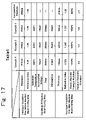
- FIG. 17 shows the results of the experiments on modification (of porous insulation films) when the porous insulation films are irradiated with electron beams;
- FIG. 18 shows the results of the experiments on modification (of porous insulation films) when the porous insulation films are irradiated with ultraviolet light
- FIG. 19 is a diagram showing a structural model of a semiconductor device
- FIG. 20 is a diagram showing conditions for simulation together with a cross-sectional structure.
- FIG. 21 shows the results of simulation performed under the conditions shown in FIG. 20 .
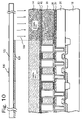
- FIG. 1 is a cross-sectional view of a semiconductor device according to a first embodiment of the present invention.
- an interlayer insulation film 26 in the semiconductor device, an interlayer insulation film 26 , a stopper film 28 , an insulation film 36 , and an interlayer insulation film 38 are disposed in that order on a semiconductor substrate 10 .
- Element isolation films 12 are disposed on the semiconductor substrate 10
- transistors 24 are disposed in element regions 14 defined by the element isolation films 12 .
- adhesion layers 32 and conductor plugs 34 are disposed in the interlayer insulation film 26 and the stopper film 28 .
- Laminated films 48 including barrier films and seed films, and wires 50 are disposed in the insulation film 36 and the interlayer insulation film 38 .
- the wires 50 are, for example, made of copper (Cu). As described above, the wires 50 are disposed in the interlayer insulation film 38 , and the interlayer insulation film 38 and the wires 50 constitute one layer (first wiring layer 37 ).
- each transistor 24 includes a gate electrode 18 surrounded by a gate insulation film 16 and a sidewall insulation film 20 , source/drain diffusion layers 22 formed in the semiconductor substrate 10 (at both sides of the gate electrode 18 ), etc.
- the interlayer insulation film 38 (first insulation film) is, for example, made of porous silicon oxide.
- the interlayer insulation film 38 includes a modified portion 38 ′ the porous property of which is modified by irradiation of an energy beam, such as an electron beam or ultraviolet light.
- an energy beam such as an electron beam or ultraviolet light.
- the Young's modulus E is 8 GPa and the relative dielectric constant K is 2.3.
- the Young's modulus E is 15 GPa and the relative dielectric constant K is 2.6. That is, the irradiation of the energy beam increases the mechanical strength and the relative dielectric constant.
- the term “modification” means a change in the structure of a film.
- one side of a line 39 b corresponds to a “non-irradiation area” which is not irradiated with the energy beam
- the other side of the line 39 b corresponds to an “irradiation area” which is irradiated with the energy beam.
- an area with high wiring density (first area) is not irradiated with the energy beam, and an area with low wiring density (second area) is irradiated with the energy beam.
- the line 39 b corresponds to a boundary line between the first area and the second area.
- the wiring density is a ratio of the area occupied by the wires to the cross-sectional area of the wiring layer.
- the ratio of the area occupied by wiring portions corresponds to the wiring density.
- the cross section 37 a is a plane parallel to a plane exposed when the interlayer insulation film 38 is formed (i.e., a plane parallel to the principal surface of the semiconductor substrate 10 ). Consequently, for example, at the design stage, one cross section in the wiring layer 37 is divided into a plurality of isometric regions, and the wiring density is calculated for each region. Thus, the “non-irradiation area” can be determined.
- the wiring density is a ratio of the area in which the wiring portion is exposed (wiring area) to the area of one region (total area).
- the non-irradiation area corresponds to an area obtained by extending the periphery of the “minimum-pitched wiring area” by a distance of a half of the minimum pitch between wires (L/2). Furthermore, the non-irradiation area may be defined as the same area as the “minimum-pitched wiring area”. Furthermore, the non-irradiation area may be defined as an area obtained by extending by a predetermined distance in the width direction of the wire 50 from the center of the wire 50 with respect to all wires 50 in the first wiring layer (or the wires in the “minimum-pitched wiring area” in the first wiring layer).
- the “predetermined distance” may be set to be a half of the minimum pitch between wires (L/2).
- the “non-irradiation area” is set with respect to all wires in one layer as described above, it is not necessary to perform the step of specifying a portion of the wiring, and thus the non-irradiation area can be set easily, which is advantageous.
- FIG. 2 is a top view of the first wiring layer shown in FIG. 1 .
- FIG. 1 is a cross-sectional view taken along the line X-X′ of FIG. 2 .
- An area inside the line 39 b shown in FIG. 2 corresponds to the “non-irradiation area”.
- an area inside a line 39 a may be defined as the “non-irradiation area”.
- the energy beam is applied only to the area with low wiring density (i.e., sparsely wired area) other than the area with high wiring density (i.e., densely wired area).
- FIGS. 3A to 16 are each a cross-sectional view showing a step in the method for fabricating the semiconductor device according to the first embodiment.
- element isolation films 12 and transistors 24 are formed in a semiconductor substrate 10 . Specifically, for example, the formation is performed in the following manner.
- the element isolation films 12 are formed in the semiconductor substrate 10 , for example, by a local oxidation of silicon (LOCOS) process (Step 1-1).
- the element isolation films 12 define element regions 14 .
- the semiconductor substrate 10 for example, a silicon substrate is used.
- the transistors 24 are formed in the element regions 14 (step 1-2). Specifically, gate electrodes 18 are formed on the element regions 14 with a gate insulation film 16 therebetween. Then, sidewall insulation films 20 are formed on the sides of the gate electrodes 18 . Subsequently, a dopant impurity is implanted into the semiconductor substrate 10 using the sidewall insulation films 20 and the gate electrodes 18 as masks, and thus source/drain diffusion layers 22 are formed in the semiconductor substrate 10 (at both sides of each gate electrode 18 ). Thereby, the transistors 24 , each having the gate electrode 18 and the source/drain diffusion layers 22 , are formed.
- an interlayer insulation film 26 As shown in FIG. 3B , an interlayer insulation film 26 , a stopper film 28 , and contact holes 30 are formed. Specifically, for example, the formation is performed in the following manner.
- the interlayer insulation film 26 made of a silicon oxide film is formed, for example, by CVD, over the entire surface of the substrate (step 2-1).
- the term “entire surface of the substrate” means an entire surface, which is provided with the element isolation films 12 and the transistors 24 , of the semiconductor substrate 10 .
- the semiconductor substrate 10 provided with the insulation films, etc. is, for convenience sake, referred to as the “substrate”.
- One surface of the substrate is referred to as the “surface of the substrate”, and the entire surface of one surface of the substrate is referred to as the “entire surface of the substrate”.
- the stopper film 28 for example, with a thickness of 50 nm is formed on the interlayer insulation film 26 (step 2-2).
- the stopper film 28 may be made of a SiN film, a hydrogenated SiC film (SiC:H film), an oxygen-doped hydrogenated SiC film (SiC:O:H film), a nitrogen-doped SiC film (SiC:N film), or the like, for example, formed by plasma-enhanced CVD.
- the hydrogenated SiC film is a SiC film in which hydrogen atoms (H) are present.
- the oxygen-doped hydrogenated SiC film is a SiC film in which oxygen atoms (O) and hydrogen atoms (H) are present.
- the nitrogen-doped SiC film is a SiC film in which nitrogen atoms (N) are present.
- the stopper film 28 functions as a stopper when a film (tungsten film) embedded in the contact holes 30 formed in the interlayer insulation film 26 is polished in the step described below.
- the stopper film 28 also functions as an etching stopper when trenches 46 are formed in the interlayer insulation film 38 , etc. in the step described below.
- step 2-3 Next, using photolithography, the contact holes 30 extending to the source/drain diffusion layers 22 are formed (step 2-3).
- adhesion layers 32 and conductor plugs 34 are formed. Specifically, for example, the formation is performed in the following manner.
- a film (not shown) for forming the adhesion layers 32 is formed over the entire surface of the substrate, for example, by sputtering (step 3-1).
- the film is made of TiN with a thickness of 50 nm and ensures adhesion of the conductor plugs 34 and their underlayers (surfaces of the contact holes 30 ).
- a tungsten film 34 (not shown), for example, with a thickness of 1 ⁇ m is formed over the entire surface of the substrate, for example, by CVD (step 3-2).
- the film for forming the adhesion layers 32 and the tungsten film 34 are polished, for example, by CMP, until the surface of the stopper film 28 is exposed. Thereby, the adhesion layers 32 are formed in the contact holes and the conductor plugs 34 made of tungsten are embedded in the contact holes.
- an insulation film 36 made of an oxygen-doped hydrogenated SiC film (SiC:O:H film) is formed.
- a SiC film is a semiconductor
- the oxygen-doped hydrogenated SiC film that contains oxygen atoms (O) and hydrogen atoms (H) is an insulator.
- the insulation film 36 made of the oxygen-doped hydrogenated SiC film is a highly dense insulation film.
- the density of the insulation film 36 is higher than that of a porous insulation film 38 which will be described below.
- the insulation film 36 also functions as a barrier film that prevents diffusion of moisture. Specifically, for example, the formation is performed in the following manner.
- step 4 First, the substrate prepared in step 3 is placed into a chamber of a plasma-enhanced CVD apparatus (not shown) (step 4-1).
- a plasma-enhanced CVD apparatus for example, a parallel-plate-type plasma-enhanced CVD apparatus is used.
- a reactive gas is introduced into the chamber (step 4-3). Specifically, first, a siloxane monomer having alkyl groups is vaporized by a vaporizer (not shown) so as to generate the reactive gas. Then, the reactive gas is introduced into the chamber using an inert gas as a carrier. In this stage, when high-frequency power is applied between plate electrodes (not shown), plasma of the reactive gas is generated, and thus the insulation film 36 made of an oxygen-doped hydrogenated SiC film is formed.
- the feed rate of the reactive gas is, for example, 1 mg/min.
- a porous interlayer insulation film (first insulation film) 38 is formed.
- the material constituting the porous interlayer insulation film 38 include (A) a porous silicon oxide film, (B) a porous silicon oxide film containing carbon, (C) an organic compound, and (D) a silicon cluster-containing insulating material. The formation methods using these materials will be described below in sequence.
- the thickness of the porous interlayer insulation film 38 is, for example, 160 nm. Specifically, for example, the formation is performed in the following manner.
- an insulation film material for forming the porous interlayer insulation film 38 is prepared (step 5A-1).
- the starting material to be used include tetraalkoxysilane, trialkoxysilane, methyltrialkoxysilane, ethyltrialkoxysilane, propyltrialkoxysilane, phenyltrialkoxysilane, vinyltrialkoxysilane, allyltrialkoxysilane, glycidyltrialkoxysilane, dialkoxysilane, dimethyldialkoxysilane, diethyldialkoxysilane, dipropyldialkoxysilane, diphenyldialkoxysilane, divinyldialkoxysilane, diallyldialkoxysilane, diglycidyldialkoxysilane, phenylmethyldialkoxysilane, phenylethyldialkoxysilane, phenylpropyltrialkoxysilane,
- the starting material is subjected to hydrolysis or polycondensation to give a polymer, and a thermally decomposable compound is added to the resulting polymer to obtain a liquid insulation film material.
- a thermally decomposable compound for example, an acrylic resin or the like is used.
- step 5-1 Next, the insulation film material obtained in step 5-1 is applied to the entire surface of the substrate, for example, by spin-coating (step 5-2).
- the spin-coating is performed, for example, at 3,000 rpm for 30 seconds.
- step 5-3 heat treatment (soft bake process) is performed (step 5-3).
- a hot plate (not shown) is used.
- the thermally decomposable compound is thermally decomposed by this treatment, and pores (voids) are formed in the interlayer insulation film 38 .
- the diameter of the pores is, for example, about 10 to 20 nm.
- the heat treatment temperature is set at 200° C. to 350° C.
- the reason for setting the heat treatment temperature at 200° C. to 350° C. is as follows.
- the thermally decomposable compound When the heat treatment temperature is set lower than 200° C., the thermally decomposable compound is not sufficiently thermally decomposed, and pores are not formed sufficiently. Furthermore, when the heat treatment temperature is set lower than 200° C., the thermal decomposition rate of the thermally decomposable compound is very slow, and a long period of time is required for forming pores. On the other hand, when the heat treatment temperature is set higher than 350° C., curing of the insulation film material advances rapidly, and the formation of pores is inhibited. For this reason, it is preferably to set the heat treatment temperature at 200° C. to 350° C. Here, the heat treatment temperature is set, for example, at 200° C. Thereby, the interlayer insulation film 38 made of the porous silicon oxide film is formed over the entire surface of the substrate.
- the formation is performed in the following manner.
- step 5B-1 First, the semiconductor substrate 10 is placed into a chamber of a plasma-enhanced CVD apparatus (not shown) (step 5B-1).
- a plasma-enhanced CVD apparatus for example, a parallel-plate-type plasma-enhanced CVD apparatus is used.
- step 5B-2 Next, the temperature of the substrate is set, for example, at 300° C. to 400° C. (step 5B-2).
- a reactive gas is introduced into the chamber (step 5B-3). Specifically, first, a siloxane monomer having alkyl groups is vaporized by a vaporizer (not shown) so as to generate the reactive gas. Then, the reactive gas is introduced into the chamber using a carrier gas. In this stage, when high-frequency power is applied between plate electrodes (not shown), plasma of the reactive gas is generated. By setting the deposition rate relatively high, the porous interlayer insulation film 38 can be formed.
- the porous interlayer insulation film 38 can be formed.
- the reactive gas for example, hexamethyldisiloxane is used.
- the feed rate of the reactive gas is, for example, 3 mg/min.
- the carrier gas CO 2 is used.
- the flow rate of the carrier gas is, for example, 6,000 sccm.
- the high-frequency power applied between plate electrodes is, for example, 13.56 MHz (500 W) and 100 kHz (500 W).
- the porous interlayer insulation film 38 made of silicon oxide film containing carbon is formed.
- the interlayer insulation film 38 made of a porous silicon oxide film containing carbon may be formed using a starting material containing thermally decomposable atomic groups (thermally decomposable compound) or oxidatively decomposable atomic groups (oxidatively decomposable compound) as will be described below.
- the film is formed with the thermally decomposable or oxidatively decomposable atomic groups being decomposed by plasma.
- step 5B′-1 First, the semiconductor substrate 10 is placed into a chamber of a plasma-enhanced CVD apparatus (not shown) (step 5B′-1).
- a plasma-enhanced CVD apparatus for example, a parallel-plate-type plasma-enhanced CVD apparatus is used.
- step 5B′-2 Next, the temperature of the substrate is set, for example, at 250° C. to 350° C. (step 5B′-2).
- step 5B′-3 reactive gases are introduced into the chamber (step 5B′-3). Specifically, first, a siloxane monomer having alkyl groups is vaporized by a vaporizer so as to generate a first reactive gas. A silane compound containing phenyl groups is vaporized by a vaporizer so as to generate a second reactive gas.
- the phenyl group is an atomic group (thermally decomposable and oxidatively decomposable atomic group) which is decomposed when subjected to an oxidation reaction under heating. Then, these reactive gases are introduced into the chamber using CO 2 gas as a carrier gas.
- the CO 2 gas is converted into plasma (oxygen plasma) to decompose the phenyl groups. Since the interlayer insulation film 38 is deposited with the phenyl groups being decomposed, the porous interlayer insulation film 38 is formed.
- Deposition conditions are set, for example, as follows.
- the first reactive gas more specifically, for example, hexamethyldisiloxane is used.
- the feed rate of the first reactive gas is, for example, 1 mg/min.
- As the second reactive gas more specifically, for example, diphenylmethylsilane is used.
- the feed rate of the second reactive gas is, for example, 1 mg/min.
- the flow rate of the carrier gas is, for example, 3,000 sccm.
- the high-frequency power applied between plate electrodes is, for example, 13.56 MHz (300 W) and 100 kHz (300 W). Thereby, the interlayer insulation film 38 made of the porous silicon oxide film containing carbon is formed.
- the porous interlayer insulation film 38 may be formed by vapor deposition using a starting material containing atomic groups that can be thermally decomposed without being oxidized or a starting material containing atomic groups that can be oxidatively decomposed without being heated.
- the formation is performed in the following manner.
- a polyaryl ether polymer containing a thermally decomposable organic compound is diluted with a solvent to form an insulation film material (step 5C-1).
- a thermally decomposable organic compound an organic compound that is thermally decomposed, for example, at 200° C. to 300° C. is used.
- examples of such an organic compound include acrylic resins, polyethylene resins, polypropylene resins, acrylic oligomers, ethylene oligomers, and propylene oligomers.
- the solvent for example, cyclohexanone is used.
- step 5C-1 Next, the insulation film material prepared in step 5C-1 is applied to the entire surface of the substrate by spin-coating (step 5C-2).
- step 5C-3 heat treatment is performed using a hot plate (not shown) (step 5C-3).
- the heat treatment temperature is, for example, 100° C. to 400° C. Thereby, the solvent in the interlayer insulation film 38 is vaporized, and a dry interlayer insulation film 38 is obtained.
- step 5C-4 the substrate obtained in step 5C-3 is placed into a curing oven (not shown) to perform heat treatment (step 5C-4).
- the heat treatment temperature is, for example, 300° C. to 400° C.
- the thermally decomposable organic compound is thermally decomposed, and pores are formed in the interlayer insulation film 38 .
- the formation is performed in the following manner.
- an insulation film material containing clusters of silica (silica cluster precursor) is prepared (step 5D-1).
- an insulation film material for example, Nano-Clustering Silica (NCS) (type: CERAMATE NCS) manufactured by Catalysts & Chemicals Ind. Co., Ltd. can be used.
- NCS Nano-Clustering Silica
- step 5D-2 Next, the insulation film material is applied to the entire surface of the substrate by spin-coating (step 5D-2).
- the spin-coating is performed, for example, at 3,000 rpm for 30 seconds.
- step 5D-3 heat treatment (soft bake process) is performed (step 5D-3).
- a hot plate (not shown) is used.
- the heat treatment temperature is, for example, 200° C.
- the heat treatment time is, for example, 150 seconds.
- the solvent in the insulation film material is vaporized, and the porous interlayer insulation film 38 is formed.
- the interlayer insulation film 38 is formed using the insulation film material containing clusters of silica, the porous interlayer insulation film 38 having fine pores is formed. Specifically, the diameter of the pores is, for example, 2 nm or less. Furthermore, since the interlayer insulation film 38 is formed using the insulation film material containing clusters of silica, the distribution of pores is highly uniform.
- the interlayer insulation film 38 By forming the interlayer insulation film 38 using the insulation film material containing clusters of silica, it is possible to form a porous interlayer insulation film 38 having very good quality. Thus, the porous interlayer insulation film made of the silicon cluster-containing insulating material can be formed.
- the insulation film material containing a silicon compound as a cluster compound has been described.
- the cluster compound is not limited to the silicon compound.
- the porous insulation film 38 is selectively irradiated with an energy beam.
- an energy beam for example, an electron beam, ultraviolet light, or the like can be used.
- the irradiation of electron beam (A) and the irradiation of ultraviolet light (B) are performed as follows.
- step 6A-1 First, the semiconductor device 10 formed in step 5 is placed into a chamber of an electron beam irradiation apparatus (not shown) (step 6A-1).
- a gas may be introduced into the chamber.
- the gas to be introduced into the chamber for example, nitrogen gas, argon gas, helium gas, methane gas, or ethane gas can be used.
- the porous insulation film 38 is selectively irradiated with an electron beam 100 (step 6A-3).
- scanning with the electron beam 100 is performed using a high-voltage generating circuit 150 , a lens excitation circuit 160 , an electron beam-scanning circuit 170 , etc., so that the porous insulation film 38 is selectively irradiated with the electron beam 100 .
- the portion of the porous interlayer insulation film 38 irradiated with the electron beam 100 is cured to lose the porous property. Specifically, pores present in the porous interlayer insulation film 38 disappear, and the mechanical strength is increased by the disappearance of the pores. On the other hand, the phenomenon of disappearance of pores leads to an increase in the relative dielectric constant of the interlayer insulation film 38 . Consequently, in this embodiment, the electron beam 100 is selectively applied only to the “portion with low wiring density” other than the portion in which it is not necessary to increase the mechanical strength (portion with high wiring density) in the interlayer insulation film 38 .
- a portion in which the distance between wires is minimum in the device (or in the wiring layer where the wires are present) is identified, and the identified portion and its surrounding portion are specified as a “non-irradiation area”.
- the electron beam 100 is applied only to the area other than the “non-irradiation area”.
- the non-irradiation area may be set as shown in FIGS. 1 and 6 . That is, the “minimum-pitched wiring area” is extended by a distance of L/2 from the center of the outermost wire, and the extended area is set as the non-irradiation area. Note that the non-irradiation area may be set as the same as the “minimum-pitched wiring area”.
- the non-irradiation area may be set as an area including all the wires 50 in the first wiring layer and its surrounding area.
- the non-irradiation area is defined as an area obtained by extending by a “predetermined distance” in the width direction of the wires 50 from the center of the wires 50 with respect to all wires 50 in the first wiring layer.
- the “predetermined distance” is, for convenience sake, referred to as the “non-irradiation width”.
- the “non-irradiation width” can be set, for example, at a half of the minimum pitch between wires (L/2).
- non-irradiation area When the “non-irradiation area” is set with respect to all wires in one layer as described above, it is not necessary to perform the step of specifying a portion of the wiring, and thus the non-irradiation area can be set easily, which is advantageous.
- the “non-irradiation area” may be set as an area obtained by extending, by the non-irradiation width from the center of the wire 50 in the width direction of the wire 50 , the “identified wiring portion”. In such a case, it is also possible to set the non-irradiation width, for example, at a value of L/2. From the standpoint of avoiding finely subdividing the non-irradiation area, the non-irradiation width is preferably set at a value equal to or larger than L/2.
- the electron beam is not applied to the portion in which the dielectric constant must be low (densely wired portion) in the porous interlayer insulation film 38 , the porous state is not modified, and the low dielectric constant is maintained.
- the electron beam 100 is applied while performing heat treatment.
- the heat treatment temperature is, for example, 200° C. to 450° C.
- curing of the interlayer insulation film 38 is promoted, and the mechanical strength of the porous interlayer insulation film 38 can be improved.
- the acceleration voltage in the irradiation with the electron beam 100 is, for example, 10 to 20 keV.
- the acceleration voltage is lower than 10 keV, it takes a long period of time for the porous interlayer insulation film 38 to be cured.
- the acceleration voltage is higher than 20 keV, the porous interlayer insulation film 38 is greatly damaged.
- the hygroscopicity of the porous interlayer insulation film 38 may be increased, or the porous interlayer insulation film 38 may be shrunk, resulting in an unnecessary increase in the relative dielectric constant and degradation in flatness. Consequently, the acceleration voltage for the irradiation with the electron beam 100 is preferably about 10 to 20 keV.
- the acceleration voltage for the irradiation with the electron beam 100 is not limited to 10 to 20 keV.
- the acceleration voltage may be set lower than 10 keV. Even when the acceleration voltage is set higher than 20 keV, by setting the irradiation time of the electron beam 100 shorter, the porous interlayer insulation film 38 can be prevented from being damaged excessively. Thus, even when the acceleration voltage is set higher than 20 keV, by setting the irradiation time of the electron beam 100 shorter, it is possible to prevent an increase in the hygroscopicity of the porous interlayer insulation film 38 and to prevent the shrinkage of the porous interlayer insulation film 38 .
- step 6B-1 First, the semiconductor device 10 is placed into a chamber provided with an ultraviolet lamp (not shown) (step 6B-1).
- an ultraviolet lamp for example, a high-pressure mercury lamp is used.
- a gas may be introduced into the chamber.
- the gas to be introduced into the chamber for example, nitrogen gas or inert gas is used.
- the inert gas for example, argon gas is used.
- the porous insulation film 38 is selectively irradiated with ultraviolet light 101 (step 6B-3).
- a photomask 110 as shown in FIG. 6 is used.
- the photomask 110 has a structure in which a glass plate 112 is partially covered with a chrome pattern 114 .
- the ultraviolet light 101 is selectively applied through the photomask 110 to the exposed surface of the porous insulation film 38 in such a manner.
- the ultraviolet light 101 is applied to the porous interlayer insulation film 38 , the portion of the porous interlayer insulation film 38 irradiated with the ultraviolet light 101 is cured to lose the porous property.
- the ultraviolet light 101 is selectively applied only to the “portion with low wiring density” other than the portion in which it is not necessary to increase the mechanical strength (portion with high wiring density) in the interlayer insulation film 38 .
- the area to which the ultraviolet light 101 is applied is set in the same manner as in step 6A-3 described above.
- the ultraviolet light 101 is applied to the porous interlayer insulation film 38 while performing heat treatment.
- the heat treatment temperature is, for example, 200° C. to 450° C.
- curing of the interlayer insulation film 38 is promoted, and the mechanical strength of the interlayer insulation film 38 can be improved.
- the pressure during the irradiation of the ultraviolet light 101 is not limited to the vacuum.
- irradiation of the ultraviolet light 101 may be performed at normal pressure.
- the mechanical strength is made uniform and the wiring capacitance is also made uniform.
- FIG. 6 for convenience sake, the means for irradiation of the electron beam 100 and the means for irradiation of the ultraviolet light 101 are both shown. However, when the irradiation of the energy beam is performed, either one of these means is used. In the drawings subsequent to FIG. 6 , for convenience sake, the means for irradiation of the electron beam 100 is omitted, and the means for irradiation of the ultraviolet light 101 only is shown.
- a highly dense insulation film (second insulation film) 40 is formed over the entire surface of the semiconductor substrate 10 provided with the porous interlayer insulation film 38 .
- Examples of the method for forming the insulation film 40 include (A) a film formation method by plasma-enhanced CVD, (B) a film formation method by vapor-phase growth, and (C) a film formation method by spin-coating. These film formation methods will be described below in sequence.
- a method for forming the insulation film 40 made of a silicon oxide film using plasma-enhanced CVD will be described below.
- step 7A-1 First, the semiconductor substrate 10 is placed into a chamber of a plasma-enhanced CVD apparatus (not shown) (step 7A-1).
- a plasma-enhanced CVD apparatus for example, a parallel-plate-type plasma-enhanced CVD apparatus is used.
- step 7A-2 Next, the temperature of the substrate is set, for example, at 400° C. (step 7A-2).
- a reactive gas is introduced into the chamber (step 7A-3). Specifically, first, trimethylsilane is vaporized by a vaporizer (not shown) so as to generate the reactive gas. Then, the reactive gas is introduced into the chamber using an inert gas as a carrier. In this stage, when high-frequency power is applied between plate electrodes (not shown), plasma of the reactive gas is generated.
- the feed rate of the reactive gas is, for example, 1 mg/min.
- the inert gas as the carrier for example, CO 2 is used.
- the flow rate of the inert gas is, for example, 100 sccm.
- the high-frequency power applied between plate electrodes is, for example, 13.56 MHz (200 W) and 100 kHz (200 W).
- the time for applying high-frequency power between plate electrodes to generate plasma is, for example, 5 seconds.
- the density of the insulation film 40 is, for example, about 2 g/cm 3 .
- the thickness of the insulation film 40 is set, for example, at 30 nm. Thereby, the insulation film 40 composed of the silicon oxide film is formed.
- a carbon-doped silicon oxide film may be formed.
- the starting material for generating the reactive gas hexamethyldisiloxane ([(CH 3 ) 3 Si] 2 O) is used. That is, hexamethyldisiloxane is vaporized by a vaporizer (not shown) so as to generate the reactive gas. Since the procedure other than the use of hexamethyldisiloxane as the starting material for generating the reactive gas is the same as that according to steps 7A-1 to 7A-3, a description thereof will be omitted.
- a method for forming the insulation film 40 made of a hydrogenated SiC film (SiC:H film) will be described below.
- the semiconductor substrate 10 is placed into a chamber of a plasma-enhanced CVD apparatus (not shown).
- a plasma-enhanced CVD apparatus for example, a parallel-plate-type plasma-enhanced CVD apparatus is used (step 7B-1).
- step 7B-2 Next, the temperature of the substrate is set, for example, at 400° C. (step 7B-2).
- a reactive gas is introduced into the chamber (step 7B-3). Specifically, first, trimethylsilane is vaporized by a vaporizer (not shown) so as to generate the reactive gas. Then, the reactive gas is introduced into the chamber using a carrier gas. In this stage, when high-frequency power is applied between plate electrodes (not shown), plasma of the reactive gas is generated.
- the feed rate of the reactive gas is, for example, 1 mg/min.
- the inert gas as the carrier for example, nitrogen (N 2 ) is used.
- the flow rate of the inert gas is, for example, 1,000 sccm.
- the high-frequency power applied between plate electrodes is, for example, 13.56 MHz (200 W) and 100 kHz (200 W).
- the time for applying high-frequency power between plate electrodes to generate plasma is, for example, 5 seconds.
- a nitrogen-doped SiC film may be formed.
- ammonia NH 3
- step 7B-3 ammonia (NH 3 ) is used as the inert gas. Since the procedure other than the use of ammonia as the inert gas is the same as that according to steps 7B-1 to 7B-3, a description thereof will be omitted.
- an oxygen-doped hydrogenated SiC film (SiC:O:H film) may be formed.
- the oxygen-doped hydrogenated SiC film is a SiC film in which oxygen atoms (O) and hydrogen atoms (H) are present.
- carbon dioxide (CO 2 ) is used as the inert gas. Since the procedure other than the use of carbon dioxide as the inert gas is the same as that according to steps 7B-1 to 7B-3, a description thereof will be omitted.
- a method for forming the insulation film 40 made of an organic SOG film using spin-coating will be described below.
- an insulation film material for forming the organic SOG film is prepared (step 7C-1).
- an insulation film material for example, tetraethoxysilane and methyltriethoxysilane are used as starting materials.
- the starting materials are subjected to hydrolysis and condensation to produce a polymer.
- the resulting polymer is used as the insulation film material.
- step 7C-1 Next, the insulation film material obtained in step 7C-1 is applied to the entire surface of the substrate by spin-coating (step 7C-2).
- the spin-coating is performed, for example, at 3,000 rpm for 30 seconds.
- step 7C-3 heat treatment (soft bake process) is performed (step 7C-3).
- a hot plate (not shown) is used.
- the heat treatment temperature is, for example, 200° C.
- the heat treatment time is, for example, 150 seconds.
- an inorganic SOG film may be used as the insulation film 40 .
- tetraethoxysilane is used as the starting material for the insulation film material. Since the procedure other than the use of tetraethoxysilane as the starting material for the insulation film material is the same as that according to steps 7C-1 to 7C-3, a description thereof will be omitted.
- trenches 46 for embedding wires are formed in the insulation film 40 , the interlayer insulation film 38 , and the insulation film 36 using photolithography. Specifically, for example, the formation is performed in the following manner.
- a photoresist film 42 is formed over the entire surface of the substrate, for example, by spin-coating (step 8-1).
- openings 44 are formed in the photoresist film 42 using photolithography (step 8-2).
- the openings 44 are used for forming wires 50 in the first layer (first metal wires).
- the openings 44 are formed in the photoresist film 42 such that the wiring width is 100 nm and the wiring pitch is 100 nm.
- step 8-3 Next, using the photoresist film 42 as a mask, the insulation film 40 , the interlayer insulation film 38 , and the insulation film 36 are etched (step 8-3).
- the etching is performed using fluorine plasma generated from CF 4 gas and CHF 3 gas.
- the stopper film 28 functions as an etching stopper.
- the trenches 46 for embedding the wires are formed in the insulation film 40 , the interlayer insulation film 38 , and the insulation film 36 .
- the upper surfaces of the conductor plugs 34 are exposed to the trenches 46 .
- the photoresist film 42 is removed.
- an insulation film 52 serving as a barrier film is formed. Specifically, for example, the formation is performed in the following manner.
- a laminated film 48 including a barrier film and a seed film is formed (step 9-1). Specifically, first, a barrier film (not shown) made of TaN with a thickness of 10 nm is formed over the entire surface of the substrate, for example, by sputtering. The barrier film prevents Cu in the wires, which will be described below, from being diffused into the insulation films. Next, a seed film (not shown) made of Cu with a thickness of 10 nm is formed over the entire surface of the substrate, for example, by sputtering. The seed film functions as an electrode when wires made of Cu are formed by electroplating. Thus, the laminated film 48 including the barrier film and the seed film is formed.
- a Cu film 50 with a thickness of 600 nm is formed, for example, by electroplating (step 9-2).
- the Cu film 50 and the laminated film 48 are polished, for example, by CMP until the surface of the insulation film is exposed (step 9-3).
- the wires 50 made of Cu are embedded in the trenches.
- Such a process of forming the wires 50 is referred to as a single damascene process.
- an insulation film 52 made of an oxygen-doped hydrogenated SiC film with a thickness of 30 nm is formed over the entire surface of the substrate, for example, by plasma-enhanced CVD (step 9-4).
- the insulation film 52 functions as a barrier film that prevents diffusion of moisture. Moisture is prevented from reaching the porous interlayer insulation film 38 by the insulation film 52 .
- the oxygen-doped hydrogenated SiC film is formed, for example, by the following steps.
- the semiconductor substrate 10 is placed into a chamber of a plasma-enhanced CVD apparatus (not shown) (step 9-4-1).
- a plasma-enhanced CVD apparatus for example, a parallel-plate-type plasma-enhanced CVD apparatus is used.
- the temperature of the substrate is set, for example, at 400° C. (step 9-4-2).
- trimethylsilane is vaporized by a vaporizer so as to generate a reactive gas (step 9-4-3).
- the reactive gas is introduced into the chamber using a carrier gas (step 9-4-4). In this stage, when high-frequency power is applied between plate electrodes (not shown), plasma of the reactive gas is generated.
- the deposition rate of the reactive gas is, for example, 1 mg/min.
- the carrier gas for example, CO 2 is used.
- the flow rate of the carrier gas is, for example, 100 sccm.
- the high-frequency power applied between plate electrodes is, for example, 13.56 MHz (200 W) and 100 kHz (200 W).
- the time for applying high-frequency power between plate electrodes to generate plasma is, for example, 5 seconds. Thereby, the insulation film 52 functioning as the barrier film is formed.
- an energy beam is selectively applied to the interlayer insulation film 54 .
- the formation is performed in the following manner.
- the interlayer insulation film 54 is formed.
- the interlayer insulation film 54 is formed, for example, by the same method as that for forming the interlayer insulation film 38 described above (step 10 ⁇ 1 ).
- the thickness of the interlayer insulation film 54 is, for example, 140 nm.
- step 2 Next, scanning of an electron beam 100 is performed, for example, using the apparatus as shown in FIG. 6 , and the “electron beam 100 ” is selectively applied to the interlayer insulation film 54 (step 10-2).
- the irradiation of the electron beam 100 is performed under the same conditions as those in the case in which the interlayer insulation film 38 is irradiated with the electron beam 100 (step 6A-3).
- irradiation of “ultraviolet light 101 ” may be performed using a photomask 120 as shown in FIG. 10 . That is, the “ultraviolet light 101 ” is selectively applied to the portion with low wiring density in the porous interlayer insulation film 54 .
- the irradiation of the ultraviolet light 101 is performed under the same conditions as those in the case in which the interlayer insulation film 38 is irradiated with the ultraviolet light 101 (step 6B-3).
- the mechanical strength is made uniform and the wiring capacitance is also made uniform.
- an insulation film 56 and a stopper film 57 are formed on the interlayer insulation film 54 .
- the insulation film 56 is formed (step 11-1).
- the insulation film 56 is a highly dense film. Specifically, the insulation film 56 is formed over the entire surface of the porous interlayer insulation film 54 .
- the insulation film 56 is formed, for example, by the same method as that for the insulation film 40 described above.
- As the material for the insulation film 56 for example, an oxygen-doped hydrogenated SiC film is used.
- the thickness of the insulation film 56 is, for example, 30 nm.
- the stopper film 57 for example, made of a silicon nitride film (SiN x ) is formed (step 11-2).
- the stopper film 57 functions as an etching stopper when contact holes 66 are formed in an interlayer insulation film 58 , etc. in the step described below.
- a silicon thermal oxide film (SiO 2 ) or the like that has different etching characteristics from the interlayer insulation film 58 , which will be described below, may also be used.
- an energy beam is selectively applied to the interlayer insulation film 58 .
- the formation is performed in the following manner.
- the interlayer insulation film 58 is formed.
- the interlayer insulation film 58 is formed, for example, by the same method as that for forming the interlayer insulation film 38 descried above (step 12-1).
- the thickness of the interlayer insulation film 58 is, for example, 140 nm.
- step 122 Next, scanning of an electron beam 100 is performed using the apparatus as shown in FIG. 12 , and the “electron beam 100 ” is selectively applied to the interlayer insulation film 58 (step 12-2).
- the irradiation of the electron beam 100 is performed under the same conditions as those in the case in which the interlayer insulation film 38 is irradiated with the electron beam 100 (step 6A-3).
- the irradiation of the interlayer insulation film 58 with the electron beam 100 is performed on the basis of the arrangement of wires 76 a , which will be described below, and, for example, areas shown in FIG. 12 are irradiated.
- irradiation of “ultraviolet light 101 ” may be performed using a photomask 120 as shown in FIG. 12 . That is, the “ultraviolet light 101 ” is selectively applied to the portion with low wiring density in the porous interlayer insulation film 58 .
- the irradiation of the ultraviolet light 101 is performed under the same conditions as those in the case in which the interlayer insulation film 38 is irradiated with the ultraviolet light 101 (step 6B-3).
- the irradiation of the interlayer insulation film 58 with the ultraviolet light 101 is performed on the basis of the arrangement of wires 76 a , which will be described below, and, for example, areas shown in FIG. 12 are irradiated.
- the mechanical strength is made uniform and the wiring capacitance is also made uniform.
- an insulation film 60 is formed on the interlayer insulation film 58 .
- the insulation film 60 is a highly dense film.
- the insulation film 60 is formed over the entire surface of the interlayer insulation film 58 .
- the insulation film 60 is formed, for example, by the same method as that for the insulation film 40 described above.
- As the material for the insulation film 60 for example, an oxygen-doped hydrogenated SiC film is used.
- the thickness of the insulation film 60 is, for example, 30 nm.
- trenches 64 for embedding wires are formed in the insulation films 52 , 56 , and 60 and the interlayer insulation films 52 and 58 .
- the formation is performed in the following manner.
- a photoresist film 62 is formed over the entire surface of the substrate, for example, by spin-coating (step 14-1).
- openings 64 are formed in the photoresist film 62 using photolithography (step 14-2).
- the openings 64 are used for forming contact holes 64 that extend to the wires 50 .
- step 14-3 Next, using the photoresist film 62 as a mask, the insulation film 60 , the interlayer insulation film 58 , the insulation film 56 , the interlayer insulation film 54 , and the insulation film 52 are etched (step 14-3).
- the etching is performed using fluorine plasma generated from CF 4 gas and CHF 3 gas.
- fluorine plasma generated from CF 4 gas and CHF 3 gas.
- trenches 72 for embedding wires are formed in the insulation film 60 , the interlayer insulation film 58 , and the insulation film 56 .
- the formation is performed in the following manner.
- openings 70 are formed in a photoresist film 68 (step 15-1).
- the openings 70 are used for forming wires 76 a in the second layer (second metal wires), which will be described below.
- step 15-2 Next, using the photoresist film 68 as a mask, the insulation film 60 , the interlayer insulation film 58 , and the insulation film 56 are etched (step 15-2).
- the etching is performed using fluorine plasma generated from CF 4 gas and CHF 3 gas.
- the trenches 72 for embedding the wires 76 a in the insulation film 60 , the interlayer insulation film 58 , and the insulation film 56 are formed.
- the trenches 72 are connected to the contact holes 66 .
- steps 14 and 15 the example in which the contact holes 66 are formed first, and then the trenches 72 are formed has been described.
- the trenches 72 may be formed first, and then the contact holes 66 may be formed.
- first, using photolithography trenches 72 are formed in the insulation film 60 , the interlayer insulation film 58 , and the insulation film 56 .
- a photoresist film (not shown) is formed on the substrate provided with the trenches 72 so as to fill the trenches 72 .
- contact holes that reach the wires 50 are formed in the interlayer insulation film 54 and the insulation film 52 .
- the stopper 57 is not required.
- an insulation film that functions as a barrier film is formed. Specifically, for example, the formation is performed in the following manner.
- a laminated film 74 including a barrier film and a seed film is formed (step 16-1). Specifically, first, a barrier film (not shown) made of TaN with a thickness of 10 nm is formed over the entire surface of the substrate, for example, by sputtering. The barrier film prevents Cu in the wires 76 a and conductor plugs 76 b , which will be described below, from being diffused into the insulation films. Next, a seed film (not shown) made of Cu with a thickness of 10 nm is formed over the entire surface of the substrate, for example, by sputtering. The seed film functions as an electrode when the wires 76 a and conductor plugs 76 b made of Cu are formed by electroplating. Thus, the laminated film 74 including the barrier film and the seed film is formed.
- a Cu film 76 with a thickness of 1,400 nm is formed, for example, by electroplating (step 16-2).
- the Cu film 76 and the laminated film 74 are polished, for example, by CMP until the surface of the insulation film 60 is exposed (step 16-3).
- the conductor plugs 76 b made of Cu are embedded in the contact holes 66 and the wires 76 a made of Cu are embedded in the trenches 72 .
- the conductor plugs 76 b and the wires 76 a are integrally formed. Such a process in which the conductor plugs 76 b and the wires 76 a are formed simultaneously is referred to as a dual damascene process.
- an insulation film 78 made of an oxygen-doped hydrogenated SiC film with a thickness of 30 nm is formed over the entire surface of the substrate, for example, by plasma-enhanced CVD (step 16-4).
- the insulation film 78 is formed, for example, by the same method as that for forming the insulation film 36 described above (steps 4-1 to 4-3).
- the insulation film 78 functions as a barrier film that prevents diffusion of moisture.
- wires in a third layer (third metal wiring layer), which is not shown, are formed. Thereby, the semiconductor device according to this embodiment is fabricated.
- the energy beam is applied to the portion with low wiring density in each of the interlayer insulation films 38 , 54 , and 58 , and thus some area (portion with low wiring density) of each of the porous interlayer insulation films 38 , 54 , and 58 is cured.
- the portion with high wiring density in each of the interlayer insulation films 38 , 54 , and 58 is not irradiated with the electron beam 100 or ultraviolet light 101 so as to maintain its porous property.
- the mechanical strength is increased only in the portions with low wiring density (portions having low mechanical strength and low wiring capacitance) of the interlayer insulation films 38 , 54 , and 58 .
- the mechanical strength is made uniform over the entire films.
- the wiring capacitance is increased only in the portions with low wiring density of the interlayer insulation films 38 , 54 , and 58 .
- the wiring capacitance is also made uniform over the entire films.
- an insulation film material was prepared in the following manner (step V1). Specifically, first, 20.8 g (0.1 mol) of tetraethoxysilane, 17.8 g (0.1 mol) of methyltriethoxysilane, 23.6 g (0.1 mol) of glycidoxypropyltrimethoxysilane, and 39.6 g of methyl isobutyl ketone were placed in a 200-ml reactor (not shown), and 16.2 g of a 1% aqueous solution of tetrabutyl ammonium hydroxide was added dropwise thereto over 10 minutes (step V1-1). After dropping was completed, an aging reaction was carried out for 2 hours (step V1-2).
- step V1-3 5 g of magnesium sulfate was added thereto to remove excess moisture (step V1-3). Then, using a rotary evaporator, ethanol generated during the aging reaction was removed so that the total amount of the reaction solution was 50 ml (step V1-4). Methyl isobutyl ketone (20 ml) was added to the resulting reaction solution to give an insulation film material (porous silica precursor) (step V1-5).
- step V2 the insulation film material prepared in step V1 was applied onto a silicon wafer (semiconductor substrate) by spin-coating (step V2).
- the coating was performed at a revolution speed of 3,000 rpm with a revolution time of 30 seconds.
- step V3 heat treatment (soft bake process) was performed at 200° C. to form a porous interlayer insulation film (step V3).
- the thickness of the porous insulation film in each example is shown in Table 1 ( FIG. 17 ).
- the refractive index of the porous insulation film at this stage is also shown in Table 1.
- step V4 the porous interlayer insulation film was irradiated with an electron beam (step V4).
- the substrate temperature, acceleration voltage, electron beam irradiation time, and atmosphere in the chamber in this step were set as shown in Table 1.
- a porous interlayer insulation film was formed as in Examples 1 to 3 except that step V4 (electron beam curing step) was not performed as shown in Table 1.
- the resulting interlayer insulation film was measured, and the results shown in Table 1 were obtained.
- Table 1 the film thickness is decreased and the elastic modulus and hardness are greatly increased compared with Comparative Example. This makes it possible to assume that the density of the interlayer insulation film is increased by the irradiation of electron beam, and as a result, the elastic modulus and hardness of the interlayer insulation film are greatly increased. Furthermore, it has also been confirmed that the relative dielectric constant is increased by the irradiation of electron beam.
- the resulting interlayer insulation film was measured, and the results shown in Table 2 ( FIG. 18 ) were obtained.
- Table 2 Table 2
- the elastic modulus and hardness of the interlayer insulation film are greatly increased and the relative dielectric constant of the interlayer insulation film is also increased by the irradiation of ultraviolet light.
- FIG. 19 shows a structural model of a semiconductor device (conductor plugs and insulation films not subjected to modification are not shown), and FIG. 20 is a diagram showing conditions for simulation together with a cross-sectional structure.
- FIG. 21 shows the results of simulation performed under the conditions shown in FIG. 20 . As shown in FIGS.
- principal components of a semiconductor substrate 80 include a silicon substrate 90 , wires 92 a , 92 b , 92 c , and 92 d (first metal wiring layer), wires 94 a , 94 b , 94 c , and 94 d (second metal wiring layer), wires 96 a , 96 b , 96 c , and 96 d (third metal wiring layer), and interlayer insulation films 82 , 83 , 84 , 85 , and 86 .
- the Young's modulus of the portion not modified is 8 Gpa and the Young's modulus of the modified portion is 15 Gpa.
- a weight of 1.6 Gpa is applied to the substrate from above.
- the second metal wiring layer is shown in a manner rotated by 90 degrees with respect to the actual arrangement.
- Simulation (1) shows the results of simulation in which a wire having the same shape of that of the wire 94 b is added to the center of the insulation film 84 shown in FIG. 20 . That is, in simulation (1), the case in which the wires were arranged at the minimum wiring pitch so that the wiring density was highest was assumed. With respect to simulations (2) to (4), simulation was performed on the structure shown in FIG. 20 .
Abstract
Description
Claims (7)
Priority Applications (1)
| Application Number | Priority Date | Filing Date | Title |
|---|---|---|---|
| US12/768,823 US20100210106A1 (en) | 2006-11-24 | 2010-04-28 | Semiconductor device having a interlayer insulation film with low dielectric constant and high mechanical strength |
Applications Claiming Priority (2)
| Application Number | Priority Date | Filing Date | Title |
|---|---|---|---|
| JP2006317446A JP5326202B2 (en) | 2006-11-24 | 2006-11-24 | Semiconductor device and manufacturing method thereof |
| JP2006-317446 | 2006-11-24 |
Related Child Applications (1)
| Application Number | Title | Priority Date | Filing Date |
|---|---|---|---|
| US12/768,823 Division US20100210106A1 (en) | 2006-11-24 | 2010-04-28 | Semiconductor device having a interlayer insulation film with low dielectric constant and high mechanical strength |
Publications (2)
| Publication Number | Publication Date |
|---|---|
| US20080122121A1 US20080122121A1 (en) | 2008-05-29 |
| US7732927B2 true US7732927B2 (en) | 2010-06-08 |
Family
ID=39462841
Family Applications (2)
| Application Number | Title | Priority Date | Filing Date |
|---|---|---|---|
| US11/944,053 Expired - Fee Related US7732927B2 (en) | 2006-11-24 | 2007-11-21 | Semiconductor device having a interlayer insulation film with low dielectric constant and high mechanical strength |
| US12/768,823 Abandoned US20100210106A1 (en) | 2006-11-24 | 2010-04-28 | Semiconductor device having a interlayer insulation film with low dielectric constant and high mechanical strength |
Family Applications After (1)
| Application Number | Title | Priority Date | Filing Date |
|---|---|---|---|
| US12/768,823 Abandoned US20100210106A1 (en) | 2006-11-24 | 2010-04-28 | Semiconductor device having a interlayer insulation film with low dielectric constant and high mechanical strength |
Country Status (2)
| Country | Link |
|---|---|
| US (2) | US7732927B2 (en) |
| JP (1) | JP5326202B2 (en) |
Families Citing this family (25)
| Publication number | Priority date | Publication date | Assignee | Title |
|---|---|---|---|---|
| US20060103023A1 (en) * | 2004-11-12 | 2006-05-18 | International Business Machines Corporation | Methods for incorporating high k dielectric materials for enhanced SRAM operation and structures produced thereby |
| WO2010065457A2 (en) * | 2008-12-02 | 2010-06-10 | Arizona Board Of Regents, For And On Behalf Of Arizona State University | Method of providing a semiconductor device with a dielectric layer and semiconductor device thereof |
| US8252659B2 (en) * | 2008-12-02 | 2012-08-28 | Imec | Method for producing interconnect structures for integrated circuits |
| US9601530B2 (en) | 2008-12-02 | 2017-03-21 | Arizona Board Of Regents, A Body Corporated Of The State Of Arizona, Acting For And On Behalf Of Arizona State University | Dual active layer semiconductor device and method of manufacturing the same |
| US9991311B2 (en) | 2008-12-02 | 2018-06-05 | Arizona Board Of Regents On Behalf Of Arizona State University | Dual active layer semiconductor device and method of manufacturing the same |
| US9721825B2 (en) | 2008-12-02 | 2017-08-01 | Arizona Board Of Regents, A Body Corporate Of The State Of Arizona, Acting For And On Behalf Of Arizona State University | Method of providing a flexible semiconductor device and flexible semiconductor device thereof |
| WO2010065459A2 (en) * | 2008-12-02 | 2010-06-10 | Arizona Board Of Regents, For And On Behalf Of Arizona State University | Method of etching organosiloxane dielectric material and semiconductor device thereof |
| JP2010245156A (en) * | 2009-04-02 | 2010-10-28 | Panasonic Corp | Method for manufacturing semiconductor device |
| KR101362025B1 (en) | 2009-05-29 | 2014-02-13 | 아리조나 보드 오브 리젠츠 퍼 앤 온 비하프 오브 아리조나 스테이트 유니버시티 | Method of providing a flexible semiconductor device at high temperatures and flexible semiconductor device thereof |
| WO2012021196A2 (en) | 2010-05-21 | 2012-02-16 | Arizona Board Of Regents, For And On Behalf Of Arizona State University | Method for manufacturing electronic devices and electronic devices thereof |
| WO2012021197A2 (en) | 2010-05-21 | 2012-02-16 | Arizona Board Of Regents, For And On Behalf Of Arizona State University | Method of manufacturing electronic devices on both sides of a carrier substrate and electronic devices thereof |
| WO2011158704A1 (en) * | 2010-06-18 | 2011-12-22 | Semiconductor Energy Laboratory Co., Ltd. | Method for manufacturing semiconductor device |
| JP6197381B2 (en) * | 2013-06-05 | 2017-09-20 | 富士通セミコンダクター株式会社 | Semiconductor device and manufacturing method thereof |
| WO2017034645A2 (en) | 2015-06-09 | 2017-03-02 | ARIZONA BOARD OF REGENTS, a body corporate for THE STATE OF ARIZONA for and on behalf of ARIZONA STATE UNIVERSITY | Method of providing an electronic device and electronic device thereof |
| US10381224B2 (en) | 2014-01-23 | 2019-08-13 | Arizona Board Of Regents On Behalf Of Arizona State University | Method of providing an electronic device and electronic device thereof |
| WO2015156891A2 (en) | 2014-01-23 | 2015-10-15 | Arizona Board Of Regents, Acting For And On Behalf Of Arizona State University | Method of providing a flexible semiconductor device and flexible semiconductor device thereof |
| KR102466741B1 (en) | 2014-05-13 | 2022-11-15 | 아리조나 보드 오브 리젠츠 온 비하프 오브 아리조나 스테이트 유니버시티 | Method of providing an electronic device |
| KR102304724B1 (en) * | 2014-12-19 | 2021-09-27 | 삼성디스플레이 주식회사 | Thin film transistor substrate, display apparatus comprising the same, method for manufacturing thin film transistor substrate, and method for manufacturing display apparatus using the same |
| US10446582B2 (en) | 2014-12-22 | 2019-10-15 | Arizona Board Of Regents On Behalf Of Arizona State University | Method of providing an imaging system and imaging system thereof |
| US9741742B2 (en) | 2014-12-22 | 2017-08-22 | Arizona Board Of Regents, A Body Corporate Of The State Of Arizona, Acting For And On Behalf Of Arizona State University | Deformable electronic device and methods of providing and using deformable electronic device |
| US9773866B2 (en) | 2015-06-18 | 2017-09-26 | Qualcomm Incorporated | Semiconductor integrated circuits (ICs) employing localized low dielectric constant (low-K) material in inter-layer dielectric (ILD) material for improved speed performance |
| EP3270411A1 (en) * | 2015-07-08 | 2018-01-17 | IMEC vzw | Method for producing an integrated circuit device with enhanced mechanical properties |
| US10157780B2 (en) * | 2016-11-29 | 2018-12-18 | Taiwan Semiconductor Manufacturing Company, Ltd. | Method of forming a device having a doping layer and device formed |
| US10396042B2 (en) | 2017-11-07 | 2019-08-27 | International Business Machines Corporation | Dielectric crack stop for advanced interconnects |
| JP2021005675A (en) * | 2019-06-27 | 2021-01-14 | ソニーセミコンダクタソリューションズ株式会社 | Semiconductor device, electronic apparatus, and manufacturing method of semiconductor device |
Citations (4)
| Publication number | Priority date | Publication date | Assignee | Title |
|---|---|---|---|---|
| JP2003100757A (en) | 2001-09-27 | 2003-04-04 | Toshiba Corp | Semiconductor device and method for manufacturing the same |
| US20030116854A1 (en) * | 2001-12-26 | 2003-06-26 | Kabushiki Kaisha Toshiba | Semiconductor device and method for manufacturing the same |
| JP2004179386A (en) | 2002-11-27 | 2004-06-24 | Seiko Epson Corp | Semiconductor device and its manufacturing method |
| US20050124151A1 (en) * | 2003-12-04 | 2005-06-09 | Taiwan Semiconductor Manufacturing Co. | Novel method to deposit carbon doped SiO2 films with improved film quality |
Family Cites Families (12)
| Publication number | Priority date | Publication date | Assignee | Title |
|---|---|---|---|---|
| JPH0855913A (en) * | 1994-06-07 | 1996-02-27 | Texas Instr Inc <Ti> | Selective filling method for void in submicron interconnection |
| JP3159093B2 (en) * | 1996-12-25 | 2001-04-23 | 日本電気株式会社 | Semiconductor device and method of manufacturing the same |
| JP2910713B2 (en) * | 1996-12-25 | 1999-06-23 | 日本電気株式会社 | Method for manufacturing semiconductor device |
| US6342454B1 (en) * | 1999-11-16 | 2002-01-29 | International Business Machines Corporation | Electronic devices with dielectric compositions and method for their manufacture |
| JP3502362B2 (en) * | 2001-05-25 | 2004-03-02 | Necマイクロシステム株式会社 | Semiconductor device and layout method thereof |
| JP2003209169A (en) * | 2002-01-17 | 2003-07-25 | Matsushita Electric Ind Co Ltd | Manufacturing method of semiconductor device |
| TW200428470A (en) * | 2003-06-05 | 2004-12-16 | Semiconductor Leading Edge Tec | Method for manufacturing semiconductor device |
| DE10360933A1 (en) * | 2003-12-23 | 2005-07-28 | Infineon Technologies Ag | Method for producing a capacitance in a layer of low-k material |
| CN1787186A (en) * | 2004-12-09 | 2006-06-14 | 富士通株式会社 | Semiconductor device fabrication method |
| JP4455356B2 (en) * | 2005-01-28 | 2010-04-21 | Necエレクトロニクス株式会社 | Semiconductor device |
| JP5204370B2 (en) * | 2005-03-17 | 2013-06-05 | ルネサスエレクトロニクス株式会社 | Semiconductor device and manufacturing method thereof |
| US7994069B2 (en) * | 2005-03-31 | 2011-08-09 | Freescale Semiconductor, Inc. | Semiconductor wafer with low-K dielectric layer and process for fabrication thereof |
-
2006
- 2006-11-24 JP JP2006317446A patent/JP5326202B2/en not_active Expired - Fee Related
-
2007
- 2007-11-21 US US11/944,053 patent/US7732927B2/en not_active Expired - Fee Related
-
2010
- 2010-04-28 US US12/768,823 patent/US20100210106A1/en not_active Abandoned
Patent Citations (4)
| Publication number | Priority date | Publication date | Assignee | Title |
|---|---|---|---|---|
| JP2003100757A (en) | 2001-09-27 | 2003-04-04 | Toshiba Corp | Semiconductor device and method for manufacturing the same |
| US20030116854A1 (en) * | 2001-12-26 | 2003-06-26 | Kabushiki Kaisha Toshiba | Semiconductor device and method for manufacturing the same |
| JP2004179386A (en) | 2002-11-27 | 2004-06-24 | Seiko Epson Corp | Semiconductor device and its manufacturing method |
| US20050124151A1 (en) * | 2003-12-04 | 2005-06-09 | Taiwan Semiconductor Manufacturing Co. | Novel method to deposit carbon doped SiO2 films with improved film quality |
Also Published As
| Publication number | Publication date |
|---|---|
| US20080122121A1 (en) | 2008-05-29 |
| JP2008130991A (en) | 2008-06-05 |
| JP5326202B2 (en) | 2013-10-30 |
| US20100210106A1 (en) | 2010-08-19 |
Similar Documents
| Publication | Publication Date | Title |
|---|---|---|
| US7732927B2 (en) | Semiconductor device having a interlayer insulation film with low dielectric constant and high mechanical strength | |
| US7262142B2 (en) | Semiconductor device fabrication method | |
| US7030468B2 (en) | Low k and ultra low k SiCOH dielectric films and methods to form the same | |
| JP5511781B2 (en) | Method for forming multiphase ultra-low dielectric film | |
| US7265437B2 (en) | Low k dielectric CVD film formation process with in-situ imbedded nanolayers to improve mechanical properties | |
| US20030232495A1 (en) | Methods and apparatus for E-beam treatment used to fabricate integrated circuit devices | |
| US20050014361A1 (en) | Dielectric materials to prevent photoresist poisoning | |
| US20040214446A1 (en) | Nitrogen-free dielectric anti-reflective coating and hardmask | |
| JP2004172590A (en) | Silicon oxycarbide, method for growing silicon oxycarbide layer, semiconductor device, and method for manufacturing semiconductor device | |
| US20060128166A1 (en) | Semiconductor device fabrication method | |
| KR20070004966A (en) | An improved method for fabricating an ultralow dielectric constant material as an intralevel or interlevel dielectric in a semiconductor device and electronic device | |
| KR20120031955A (en) | Method of improving interlayer adhesion | |
| KR20130043096A (en) | Ultra low dielectric materials using hybrid precursors containing silicon with organic functional groups by plasma-enhanced chemical vapor deposition | |
| KR20080017285A (en) | Insulator film, manufacturing method of multilayer wiring device and multilayer wiring device | |
| JP2010267971A (en) | Dielectric barrier deposition using nitrogen containing precursor | |
| JP2001223269A (en) | Semiconductor device and manufacturing method therefor | |
| US7320945B2 (en) | Gradient low k material | |
| US20100093174A1 (en) | Method of manufacturing low-k dielectric film, and formation of air-gap using the low-k dielectric film | |
| JP4408816B2 (en) | Manufacturing method of semiconductor device | |
| KR101443999B1 (en) | Method for manufacturing semiconductor device | |
| KR101106425B1 (en) | Nitrogen-free dielectric anti-reflective coating and hardmask | |
| JP2008053402A (en) | Method of manufacturing semiconductor device |
Legal Events
| Date | Code | Title | Description |
|---|---|---|---|
| AS | Assignment |
Owner name: FUJITSU LIMITED, JAPAN Free format text: ASSIGNMENT OF ASSIGNORS INTEREST;ASSIGNORS:SUDA, SHOICHI;TOKUYO, SHINO;NAKATA, YOSHIHIRO;AND OTHERS;REEL/FRAME:020214/0011 Effective date: 20071023 Owner name: FUJITSU LIMITED,JAPAN Free format text: ASSIGNMENT OF ASSIGNORS INTEREST;ASSIGNORS:SUDA, SHOICHI;TOKUYO, SHINO;NAKATA, YOSHIHIRO;AND OTHERS;REEL/FRAME:020214/0011 Effective date: 20071023 |
|
| STCF | Information on status: patent grant |
Free format text: PATENTED CASE |
|
| FEPP | Fee payment procedure |
Free format text: PAYOR NUMBER ASSIGNED (ORIGINAL EVENT CODE: ASPN); ENTITY STATUS OF PATENT OWNER: LARGE ENTITY |
|
| FPAY | Fee payment |
Year of fee payment: 4 |
|
| MAFP | Maintenance fee payment |
Free format text: PAYMENT OF MAINTENANCE FEE, 8TH YEAR, LARGE ENTITY (ORIGINAL EVENT CODE: M1552) Year of fee payment: 8 |
|
| FEPP | Fee payment procedure |
Free format text: MAINTENANCE FEE REMINDER MAILED (ORIGINAL EVENT CODE: REM.); ENTITY STATUS OF PATENT OWNER: LARGE ENTITY |
|
| LAPS | Lapse for failure to pay maintenance fees |
Free format text: PATENT EXPIRED FOR FAILURE TO PAY MAINTENANCE FEES (ORIGINAL EVENT CODE: EXP.); ENTITY STATUS OF PATENT OWNER: LARGE ENTITY |
|
| STCH | Information on status: patent discontinuation |
Free format text: PATENT EXPIRED DUE TO NONPAYMENT OF MAINTENANCE FEES UNDER 37 CFR 1.362 |
|
| FP | Lapsed due to failure to pay maintenance fee |
Effective date: 20220608 |