US7744429B2 - Connector with plugging direction perpendicular to circuit boards - Google Patents
Connector with plugging direction perpendicular to circuit boards Download PDFInfo
- Publication number
- US7744429B2 US7744429B2 US12/142,349 US14234908A US7744429B2 US 7744429 B2 US7744429 B2 US 7744429B2 US 14234908 A US14234908 A US 14234908A US 7744429 B2 US7744429 B2 US 7744429B2
- Authority
- US
- United States
- Prior art keywords
- connector
- guiding
- connector according
- plug
- fixing portion
- Prior art date
- Legal status (The legal status is an assumption and is not a legal conclusion. Google has not performed a legal analysis and makes no representation as to the accuracy of the status listed.)
- Expired - Fee Related
Links
Images


Classifications
-
- H—ELECTRICITY
- H01—ELECTRIC ELEMENTS
- H01R—ELECTRICALLY-CONDUCTIVE CONNECTIONS; STRUCTURAL ASSOCIATIONS OF A PLURALITY OF MUTUALLY-INSULATED ELECTRICAL CONNECTING ELEMENTS; COUPLING DEVICES; CURRENT COLLECTORS
- H01R12/00—Structural associations of a plurality of mutually-insulated electrical connecting elements, specially adapted for printed circuits, e.g. printed circuit boards [PCB], flat or ribbon cables, or like generally planar structures, e.g. terminal strips, terminal blocks; Coupling devices specially adapted for printed circuits, flat or ribbon cables, or like generally planar structures; Terminals specially adapted for contact with, or insertion into, printed circuits, flat or ribbon cables, or like generally planar structures
- H01R12/70—Coupling devices
- H01R12/7005—Guiding, mounting, polarizing or locking means; Extractors
- H01R12/7011—Locking or fixing a connector to a PCB
- H01R12/7017—Snap means
- H01R12/7023—Snap means integral with the coupling device
-
- H—ELECTRICITY
- H01—ELECTRIC ELEMENTS
- H01R—ELECTRICALLY-CONDUCTIVE CONNECTIONS; STRUCTURAL ASSOCIATIONS OF A PLURALITY OF MUTUALLY-INSULATED ELECTRICAL CONNECTING ELEMENTS; COUPLING DEVICES; CURRENT COLLECTORS
- H01R12/00—Structural associations of a plurality of mutually-insulated electrical connecting elements, specially adapted for printed circuits, e.g. printed circuit boards [PCB], flat or ribbon cables, or like generally planar structures, e.g. terminal strips, terminal blocks; Coupling devices specially adapted for printed circuits, flat or ribbon cables, or like generally planar structures; Terminals specially adapted for contact with, or insertion into, printed circuits, flat or ribbon cables, or like generally planar structures
- H01R12/70—Coupling devices
- H01R12/7005—Guiding, mounting, polarizing or locking means; Extractors
- H01R12/7011—Locking or fixing a connector to a PCB
- H01R12/707—Soldering or welding
-
- H—ELECTRICITY
- H01—ELECTRIC ELEMENTS
- H01R—ELECTRICALLY-CONDUCTIVE CONNECTIONS; STRUCTURAL ASSOCIATIONS OF A PLURALITY OF MUTUALLY-INSULATED ELECTRICAL CONNECTING ELEMENTS; COUPLING DEVICES; CURRENT COLLECTORS
- H01R24/00—Two-part coupling devices, or either of their cooperating parts, characterised by their overall structure
- H01R24/60—Contacts spaced along planar side wall transverse to longitudinal axis of engagement
- H01R24/62—Sliding engagements with one side only, e.g. modular jack coupling devices
- H01R24/64—Sliding engagements with one side only, e.g. modular jack coupling devices for high frequency, e.g. RJ 45
Definitions
- the present invention relates to a connector and, in particular, to a connector for communicating transmission.
- the present electronic products usually have the communicating transmission function.
- the communicating transmission function can be carried out by a connector and a plug.
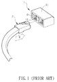
- a conventional connector for data transmission through network includes a housing 11 and a plurality of signal pins 12 .
- the housing 11 has an insert hole O, and the signal pins 12 are disposed in the insert hole O.
- the insert hole O is connected with a plug P such as an RJ-45 plug to transmit data through network.
- the plug P To connect the plug P with the connector 1 , the plug P is plugged into the insert hole O of the housing 11 along a horizontal direction H. Then, the plug P can be electrically connected with the signal pins 12 of the connector 1 so as to transmit data through network.
- the connector 1 has a large bottom size, it will occupy a certain area of a circuit board, thereby influencing the layout of the circuit board and thus limiting the space for allocating other circuitries on the circuit board.
- the present invention is to provide a connector having a pin direction the same as a plugging direction of an associated plug such that the plug can be plugged in the connector in a direction perpendicular to a circuit board. Accordingly, the layout for the connector can be reduced, and the circuit layout of the circuit board can be more flexible.
- a connector connected with a circuit board includes a housing and a main body.
- the housing has an insert hole and an accommodating portion.
- the main body is fixed in the accommodating portion and has a plurality of signal terminals and a plurality of pins arranged in the same direction.
- a plugging direction of the plug is perpendicular to the circuit board.
- the guiding portion and the fixing portion are respectively disposed at the inner circumference of the housing and the outer circumference of the main body, and the arranging directions of the signal terminals and pins can be changed so that the plugging direction of the plug is concordant as the direction of the pins and is perpendicular to the circuit board.
- a plug can be plugged in the connector of the present invention in a direction perpendicular to the circuit board. Therefore, the present invention can not only change the plugging direction of the plug, but also decrease the layout of the circuit board for the connector so as to improve the circuit layout flexibility.
- the present invention also increases the variation of disposing direction of the circuit board in the electronic device, and increases utilization of space design in the electronic device.
- FIG. 1 is a schematic diagram showing the conventional connector connected with a plug
- FIG. 2 is a schematic diagram showing a housing and a main body of a connector according to an embodiment of the present invention
- FIG. 3 is a schematic diagram showing a housing and a metal case of the connector according to the embodiment of the present invention.
- FIG. 4 is a schematic diagram showing the connector according to the embodiment of the present invention that is disposed on a an external circuit board and connected with a plug;
- FIG. 5 is a schematic diagram showing a housing and a main body of a connector according to another embodiment of the present invention.
- a connector 2 according to an embodiment of the present invention includes a housing 21 and a main body 22 .
- the connector 2 can be a network communicating connector such as an RJ-45 connector, an RJ-11 connector or an RJ-12 connector.
- the housing 21 of the connector 2 is a rectangular housing and includes an insert hole O and an accommodating portion C.
- the housing 21 further includes at least one first guiding portion 211 and at least one first fixing portion 212 disposed at inner circumference of the accommodating portion C.
- the first guiding portion 211 is, for example but not limited to, a guiding slot or a guiding track.
- the first guiding portion 211 is a guiding slot, which is integrally formed as a single piece on the inner circumference of the accommodating portion C.
- the first fixing portion 212 is, for example but not limited to, a protrusion, a concave, a clasp, a bulk or a groove.
- the first fixing portion 212 is a clasp, which is integrally formed as a single piece on the inner circumference of the accommodating portion C and located above the first guiding portion 211 .
- a bottom S 2 of the housing 21 has at least one clasp 214 for fixing the connector 2 on the circuit board.
- the housing 21 may include two clasps which have opposite clasping directions, so that the housing 21 can sustain force homogenously so as to improve the fixing stability.
- the main body 22 has a plurality of signal terminals 223 , a plurality of pins 224 , at least one second guiding portion 221 and at least one second fixing portion 222 .
- the signal terminals 223 can be electrically connected with corresponding terminals of an RJ-45 connector, an RJ-11 connector, or an RJ-12 connector.
- the pins 224 are separated from the signal terminals 223 .
- the second guiding portion 221 and the second fixing portion 222 are disposed on the outer circumference of the main body 22 and are located respectively corresponding to the first guiding portion 211 and the first fixing portion 212 .
- the second guiding portion 221 is, for example but not limited to, a guiding slot or a guiding track.
- the first guiding portion 211 is a guiding slot
- the second guiding portion 221 is correspondingly a guiding track.
- the second guiding portion 221 is integrally formed as a single piece on the outer circumference (two sides) of the main body 22 .
- the second fixing portion 222 can be, for example but not limited to, a protrusion, a concave, a clasp, a bulk or a groove.
- the second fixing portion 222 is a groove while the first fixing portion 212 is a clasp.
- the second fixing portion 222 is integrally formed as a single piece on the outer circumference of the main body 22 and located above the second guiding portion 221 .
- the designation of the first fixing portion 212 to the second fixing portion 222 can also be a combination of a protrusion and a protrusion or a combination of two clasps.
- the signal terminals 223 and the pins 224 are preferably disposed in the same direction as the first guiding portion 211 and the second guiding portion 221 .
- the signal terminals 223 or the pins 224 can be disposed in the direction different from that of the first guiding portion 211 and the second guiding portion 221 .
- the guiding slot of the first guiding portion 211 is slid along the guiding track of the second guiding portion 221 , so that the housing 21 and the main body 22 can be guided to the desired positions.
- the clasp of the first fixing portion 212 and the groove of the second fixing portion 222 are successfully fixed and assembled, thereby achieving the goals of positioning and preventing from loosing of the housing 21 and the main body 22 .
- the connector 2 can further include a metal case 23 covering the housing 21 .
- the housing 21 can further include a first fixing portion 213 disposed at the outer circumference thereof.
- the metal case 23 further has a second fixing portion 234 , which is disposed corresponding to the first fixing portion 213 and located on one side of the metal case 23 .
- Each of the first fixing portion 213 and the second fixing portion 234 can be, for example, a protrusion, a concave, a clasp, a bulk or a groove.
- the corresponding combination of the first fixing portion 213 and the second fixing portion 234 is similar to that of the first fixing portion 212 and the second fixing portion 222 described above, so the detailed description will be omitted.
- the first fixing portion 213 is a bulk and the second fixing portion 234 is a groove for example.
- the configuration of the metal case 23 can intensify the noise shielding and benefit the flatness of the bottom S 2 of the housing 21 , which can facilitate the securely connection between the housing 21 and the circuit board.
- the fourth fixing portion 234 and the third fixing portion 213 are fixed with each other. Since the signal transmitted by the signal terminals 223 is easily affected by external transmission lines during transmission, the configuration of the metal case 23 can intensify the noise shielding and benefit the flatness of the bottom S 2 of the housing 21 , which can facilitate the securely connection between the housing 21 and the circuit board.
- the clasps 214 of the housing 21 and the pins 224 of the main body 22 are perpendicular to a circuit board B and respectively inserted into the holes D 1 and the holes D.
- the connector 2 can be fixed on the circuit board B by the clasps 214 and electrically connected to the circuit board B to transmit signal through the pins 224 .
- the main body 22 further has an internal circuit board I for connecting the plurality of signal terminals 223 and the plurality of pins 224 .
- the plug P is inserted into the connector 2 along a vertical direction V, which is perpendicular to the external circuit board B and the internal circuit board I.
- the signal terminals 223 of the connector 2 are electrically connected with an electrically connecting terminal 323 of the plug P from data outputting and inputting.
- the electrically connecting terminal of the plug can be a connecting terminal of an RJ-45 plug, an RJ-11 plug or an RJ-12 plug.
- the guiding portion and the fixing portion of the present invention are respectively disposed at the inner circumference of the housing and the outer circumference of the main body, and the arranging directions of the signal terminals and pins can be changed so that the plugging direction of the plug is concordant as the direction of the pins and is perpendicular to the circuit board.
- a plug can be plugged in the connector of the present invention in a direction perpendicular to the circuit board. Therefore, the present invention can not only change the plugging direction of the plug, but also decrease the layout of the circuit board for the connector so as to improve the circuit layout flexibility.
- the present invention also increases the variation of disposing direction of the circuit board in the electronic device, and increases utilization of space design in the electronic device.
Abstract
Description
Claims (16)
Applications Claiming Priority (3)
| Application Number | Priority Date | Filing Date | Title |
|---|---|---|---|
| TW96150230A | 2007-12-26 | ||
| TW096150230A TW200929721A (en) | 2007-12-26 | 2007-12-26 | Connector |
| TW096150230 | 2007-12-26 |
Publications (2)
| Publication Number | Publication Date |
|---|---|
| US20090170355A1 US20090170355A1 (en) | 2009-07-02 |
| US7744429B2 true US7744429B2 (en) | 2010-06-29 |
Family
ID=40799033
Family Applications (1)
| Application Number | Title | Priority Date | Filing Date |
|---|---|---|---|
| US12/142,349 Expired - Fee Related US7744429B2 (en) | 2007-12-26 | 2008-06-19 | Connector with plugging direction perpendicular to circuit boards |
Country Status (3)
| Country | Link |
|---|---|
| US (1) | US7744429B2 (en) |
| JP (1) | JP2009158454A (en) |
| TW (1) | TW200929721A (en) |
Cited By (3)
| Publication number | Priority date | Publication date | Assignee | Title |
|---|---|---|---|---|
| US7993166B1 (en) * | 2010-06-01 | 2011-08-09 | Hon Hai Precision Ind. Co., Ltd. | Hybrid modular jack |
| US20120196456A1 (en) * | 2007-03-01 | 2012-08-02 | Renteria Victor H | Integrated connector apparatus and methods |
| US8480439B1 (en) * | 2011-12-20 | 2013-07-09 | Yfc-Boneagle Electric Co., Ltd. | Keystone jack |
Citations (19)
| Publication number | Priority date | Publication date | Assignee | Title |
|---|---|---|---|---|
| US5312273A (en) * | 1992-08-11 | 1994-05-17 | Molex Incorporated | Shielded modular jack |
| US5378172A (en) * | 1994-03-10 | 1995-01-03 | Molex Incorporated | Low profile shielded jack |
| US5626497A (en) * | 1994-07-14 | 1997-05-06 | Molex Incorporated | Modular jack type connector |
| US5766043A (en) * | 1996-02-29 | 1998-06-16 | Corcom, Inc. | Telephone connector |
| US6012936A (en) * | 1996-10-16 | 2000-01-11 | The Siemon Company | Switching jack |
| US6431917B1 (en) * | 1996-07-26 | 2002-08-13 | Fci Americas Technology, Inc. | Modular telephone jack |
| US6450838B2 (en) * | 2000-05-12 | 2002-09-17 | Avaya, Inc. | Universally configurable modular connector |
| US6537110B1 (en) * | 2001-11-08 | 2003-03-25 | Hon Hai Precision Ind. Co., Ltd. | Stacked modular jack assembly having highly modularized electronic components |
| US6623306B2 (en) * | 2001-12-26 | 2003-09-23 | Hon Hai Precision Ind. Co., Ltd. | Solder mask configuration for a printed circuit board of a modular jack |
| US6695649B1 (en) * | 2002-08-05 | 2004-02-24 | Panduit Corp | Vertical PCB jack with shield |
| US6786772B1 (en) * | 2003-04-16 | 2004-09-07 | Lankom Electronics Co., Ltd. | Modulated connector |
| US20050142952A1 (en) * | 2003-12-26 | 2005-06-30 | Yuan-Huei Peng | Printed circuit board jack |
| US20060128228A1 (en) * | 2004-12-10 | 2006-06-15 | Hon Hai Precision Ind. Co., Ltd. | Modular jack connector |
| US7121898B2 (en) * | 2004-06-16 | 2006-10-17 | Tyco Electronics Corporation | Shielding configuration for a multi-port jack assembly |
| US7153158B1 (en) * | 2005-07-13 | 2006-12-26 | Hon Hai Precision Ind. Co., Ltd. | Stacked module connector |
| US20070059988A1 (en) * | 1999-12-30 | 2007-03-15 | Masud Bolouri-Saransar | Electrical circuit board and a multiconnector |
| US7341492B2 (en) * | 2003-06-05 | 2008-03-11 | Hon Hai Precision Ind. Co., Ltd. | Modular jack having electrical wires through a side wall thereof |
| US7351106B2 (en) * | 2005-09-22 | 2008-04-01 | Hon Hai Precision Ind. Co., Ltd. | Electrical connector having an inner printed circuit board |
| US20080233803A1 (en) * | 2007-03-01 | 2008-09-25 | Renteria Victor H | Integrated connector apparatus and methods |
Family Cites Families (1)
| Publication number | Priority date | Publication date | Assignee | Title |
|---|---|---|---|---|
| US6083052A (en) * | 1998-03-23 | 2000-07-04 | The Siemon Company | Enhanced performance connector |
-
2007
- 2007-12-26 TW TW096150230A patent/TW200929721A/en unknown
-
2008
- 2008-03-24 JP JP2008074985A patent/JP2009158454A/en active Pending
- 2008-06-19 US US12/142,349 patent/US7744429B2/en not_active Expired - Fee Related
Patent Citations (19)
| Publication number | Priority date | Publication date | Assignee | Title |
|---|---|---|---|---|
| US5312273A (en) * | 1992-08-11 | 1994-05-17 | Molex Incorporated | Shielded modular jack |
| US5378172A (en) * | 1994-03-10 | 1995-01-03 | Molex Incorporated | Low profile shielded jack |
| US5626497A (en) * | 1994-07-14 | 1997-05-06 | Molex Incorporated | Modular jack type connector |
| US5766043A (en) * | 1996-02-29 | 1998-06-16 | Corcom, Inc. | Telephone connector |
| US6431917B1 (en) * | 1996-07-26 | 2002-08-13 | Fci Americas Technology, Inc. | Modular telephone jack |
| US6012936A (en) * | 1996-10-16 | 2000-01-11 | The Siemon Company | Switching jack |
| US20070059988A1 (en) * | 1999-12-30 | 2007-03-15 | Masud Bolouri-Saransar | Electrical circuit board and a multiconnector |
| US6450838B2 (en) * | 2000-05-12 | 2002-09-17 | Avaya, Inc. | Universally configurable modular connector |
| US6537110B1 (en) * | 2001-11-08 | 2003-03-25 | Hon Hai Precision Ind. Co., Ltd. | Stacked modular jack assembly having highly modularized electronic components |
| US6623306B2 (en) * | 2001-12-26 | 2003-09-23 | Hon Hai Precision Ind. Co., Ltd. | Solder mask configuration for a printed circuit board of a modular jack |
| US6695649B1 (en) * | 2002-08-05 | 2004-02-24 | Panduit Corp | Vertical PCB jack with shield |
| US6786772B1 (en) * | 2003-04-16 | 2004-09-07 | Lankom Electronics Co., Ltd. | Modulated connector |
| US7341492B2 (en) * | 2003-06-05 | 2008-03-11 | Hon Hai Precision Ind. Co., Ltd. | Modular jack having electrical wires through a side wall thereof |
| US20050142952A1 (en) * | 2003-12-26 | 2005-06-30 | Yuan-Huei Peng | Printed circuit board jack |
| US7121898B2 (en) * | 2004-06-16 | 2006-10-17 | Tyco Electronics Corporation | Shielding configuration for a multi-port jack assembly |
| US20060128228A1 (en) * | 2004-12-10 | 2006-06-15 | Hon Hai Precision Ind. Co., Ltd. | Modular jack connector |
| US7153158B1 (en) * | 2005-07-13 | 2006-12-26 | Hon Hai Precision Ind. Co., Ltd. | Stacked module connector |
| US7351106B2 (en) * | 2005-09-22 | 2008-04-01 | Hon Hai Precision Ind. Co., Ltd. | Electrical connector having an inner printed circuit board |
| US20080233803A1 (en) * | 2007-03-01 | 2008-09-25 | Renteria Victor H | Integrated connector apparatus and methods |
Cited By (4)
| Publication number | Priority date | Publication date | Assignee | Title |
|---|---|---|---|---|
| US20120196456A1 (en) * | 2007-03-01 | 2012-08-02 | Renteria Victor H | Integrated connector apparatus and methods |
| US8764493B2 (en) * | 2007-03-01 | 2014-07-01 | Pulse Electronics, Inc. | Integrated connector apparatus and methods |
| US7993166B1 (en) * | 2010-06-01 | 2011-08-09 | Hon Hai Precision Ind. Co., Ltd. | Hybrid modular jack |
| US8480439B1 (en) * | 2011-12-20 | 2013-07-09 | Yfc-Boneagle Electric Co., Ltd. | Keystone jack |
Also Published As
| Publication number | Publication date |
|---|---|
| JP2009158454A (en) | 2009-07-16 |
| TW200929721A (en) | 2009-07-01 |
| US20090170355A1 (en) | 2009-07-02 |
Similar Documents
| Publication | Publication Date | Title |
|---|---|---|
| US8221160B2 (en) | Connector assembly having grounding means | |
| US8308515B2 (en) | Multi-interfaces connector | |
| US7364463B1 (en) | Stacked connector assembly | |
| US8267722B2 (en) | Cable connector assembly having improved grounding member | |
| US8864526B2 (en) | Connection socket for mobile terminal | |
| JP3076829U (en) | Combination type connector | |
| US7988460B1 (en) | Electrical engagement structure of connection device | |
| US7927148B2 (en) | Electrical connector | |
| KR20100123594A (en) | Connector | |
| US8308511B2 (en) | Waterproof electrical connector | |
| US6179653B1 (en) | Stacking computer connector | |
| US7011550B1 (en) | Compound electrical connector | |
| US10925159B2 (en) | Circuit device | |
| KR100621015B1 (en) | Earphone jack and mobile communication terminal having the same | |
| US7744429B2 (en) | Connector with plugging direction perpendicular to circuit boards | |
| US20050095912A1 (en) | Connector | |
| US7264489B2 (en) | Dual connector assembly with pivoting keep-out member | |
| US9124049B2 (en) | Micro ethernet connector | |
| US20100068945A1 (en) | Modularized connector for computer | |
| US20040180574A1 (en) | Stacked connector assembly | |
| US20080299830A1 (en) | Electrical card connector assembly | |
| US20030119342A1 (en) | Rotatably mated connector couple | |
| US8281480B2 (en) | Method for manufacturing wireless receiver | |
| US6010368A (en) | Dual slot card edge connector | |
| US8403691B1 (en) | Fan connector |
Legal Events
| Date | Code | Title | Description |
|---|---|---|---|
| AS | Assignment |
Owner name: DELTA ELECTRONICS, INC., TAIWAN Free format text: ASSIGNMENT OF ASSIGNORS INTEREST;ASSIGNORS:ZHANG, ZHONG-MING;ZUO, YUN;TAI, YU-YUAN;REEL/FRAME:021122/0286 Effective date: 20080416 Owner name: DELTA ELECTRONICS, INC.,TAIWAN Free format text: ASSIGNMENT OF ASSIGNORS INTEREST;ASSIGNORS:ZHANG, ZHONG-MING;ZUO, YUN;TAI, YU-YUAN;REEL/FRAME:021122/0286 Effective date: 20080416 |
|
| STCF | Information on status: patent grant |
Free format text: PATENTED CASE |
|
| FPAY | Fee payment |
Year of fee payment: 4 |
|
| FEPP | Fee payment procedure |
Free format text: MAINTENANCE FEE REMINDER MAILED (ORIGINAL EVENT CODE: REM.) |
|
| LAPS | Lapse for failure to pay maintenance fees |
Free format text: PATENT EXPIRED FOR FAILURE TO PAY MAINTENANCE FEES (ORIGINAL EVENT CODE: EXP.); ENTITY STATUS OF PATENT OWNER: LARGE ENTITY |
|
| STCH | Information on status: patent discontinuation |
Free format text: PATENT EXPIRED DUE TO NONPAYMENT OF MAINTENANCE FEES UNDER 37 CFR 1.362 |
|
| FP | Lapsed due to failure to pay maintenance fee |
Effective date: 20220629 |