US7745339B2 - Method for forming fine pattern of semiconductor device - Google Patents
Method for forming fine pattern of semiconductor device Download PDFInfo
- Publication number
- US7745339B2 US7745339B2 US11/672,676 US67267607A US7745339B2 US 7745339 B2 US7745339 B2 US 7745339B2 US 67267607 A US67267607 A US 67267607A US 7745339 B2 US7745339 B2 US 7745339B2
- Authority
- US
- United States
- Prior art keywords
- hard mask
- mask pattern
- film
- pattern
- underlying layer
- Prior art date
- Legal status (The legal status is an assumption and is not a legal conclusion. Google has not performed a legal analysis and makes no representation as to the accuracy of the status listed.)
- Expired - Fee Related, expires
Links
Images


Classifications
-
- H—ELECTRICITY
- H01—ELECTRIC ELEMENTS
- H01L—SEMICONDUCTOR DEVICES NOT COVERED BY CLASS H10
- H01L21/00—Processes or apparatus adapted for the manufacture or treatment of semiconductor or solid state devices or of parts thereof
- H01L21/70—Manufacture or treatment of devices consisting of a plurality of solid state components formed in or on a common substrate or of parts thereof; Manufacture of integrated circuit devices or of parts thereof
- H01L21/71—Manufacture of specific parts of devices defined in group H01L21/70
- H01L21/768—Applying interconnections to be used for carrying current between separate components within a device comprising conductors and dielectrics
- H01L21/76838—Applying interconnections to be used for carrying current between separate components within a device comprising conductors and dielectrics characterised by the formation and the after-treatment of the conductors
-
- H—ELECTRICITY
- H01—ELECTRIC ELEMENTS
- H01L—SEMICONDUCTOR DEVICES NOT COVERED BY CLASS H10
- H01L21/00—Processes or apparatus adapted for the manufacture or treatment of semiconductor or solid state devices or of parts thereof
- H01L21/02—Manufacture or treatment of semiconductor devices or of parts thereof
- H01L21/027—Making masks on semiconductor bodies for further photolithographic processing not provided for in group H01L21/18 or H01L21/34
- H01L21/033—Making masks on semiconductor bodies for further photolithographic processing not provided for in group H01L21/18 or H01L21/34 comprising inorganic layers
- H01L21/0334—Making masks on semiconductor bodies for further photolithographic processing not provided for in group H01L21/18 or H01L21/34 comprising inorganic layers characterised by their size, orientation, disposition, behaviour, shape, in horizontal or vertical plane
- H01L21/0337—Making masks on semiconductor bodies for further photolithographic processing not provided for in group H01L21/18 or H01L21/34 comprising inorganic layers characterised by their size, orientation, disposition, behaviour, shape, in horizontal or vertical plane characterised by the process involved to create the mask, e.g. lift-off masks, sidewalls, or to modify the mask, e.g. pre-treatment, post-treatment
-
- H—ELECTRICITY
- H01—ELECTRIC ELEMENTS
- H01L—SEMICONDUCTOR DEVICES NOT COVERED BY CLASS H10
- H01L21/00—Processes or apparatus adapted for the manufacture or treatment of semiconductor or solid state devices or of parts thereof
- H01L21/02—Manufacture or treatment of semiconductor devices or of parts thereof
- H01L21/027—Making masks on semiconductor bodies for further photolithographic processing not provided for in group H01L21/18 or H01L21/34
- H01L21/033—Making masks on semiconductor bodies for further photolithographic processing not provided for in group H01L21/18 or H01L21/34 comprising inorganic layers
- H01L21/0334—Making masks on semiconductor bodies for further photolithographic processing not provided for in group H01L21/18 or H01L21/34 comprising inorganic layers characterised by their size, orientation, disposition, behaviour, shape, in horizontal or vertical plane
- H01L21/0338—Process specially adapted to improve the resolution of the mask
-
- H—ELECTRICITY
- H01—ELECTRIC ELEMENTS
- H01L—SEMICONDUCTOR DEVICES NOT COVERED BY CLASS H10
- H01L21/00—Processes or apparatus adapted for the manufacture or treatment of semiconductor or solid state devices or of parts thereof
- H01L21/02—Manufacture or treatment of semiconductor devices or of parts thereof
- H01L21/04—Manufacture or treatment of semiconductor devices or of parts thereof the devices having at least one potential-jump barrier or surface barrier, e.g. PN junction, depletion layer or carrier concentration layer
- H01L21/18—Manufacture or treatment of semiconductor devices or of parts thereof the devices having at least one potential-jump barrier or surface barrier, e.g. PN junction, depletion layer or carrier concentration layer the devices having semiconductor bodies comprising elements of Group IV of the Periodic System or AIIIBV compounds with or without impurities, e.g. doping materials
- H01L21/30—Treatment of semiconductor bodies using processes or apparatus not provided for in groups H01L21/20 - H01L21/26
- H01L21/31—Treatment of semiconductor bodies using processes or apparatus not provided for in groups H01L21/20 - H01L21/26 to form insulating layers thereon, e.g. for masking or by using photolithographic techniques; After treatment of these layers; Selection of materials for these layers
- H01L21/3105—After-treatment
- H01L21/311—Etching the insulating layers by chemical or physical means
- H01L21/31127—Etching organic layers
- H01L21/31133—Etching organic layers by chemical means
- H01L21/31138—Etching organic layers by chemical means by dry-etching
-
- H—ELECTRICITY
- H01—ELECTRIC ELEMENTS
- H01L—SEMICONDUCTOR DEVICES NOT COVERED BY CLASS H10
- H01L21/00—Processes or apparatus adapted for the manufacture or treatment of semiconductor or solid state devices or of parts thereof
- H01L21/02—Manufacture or treatment of semiconductor devices or of parts thereof
- H01L21/04—Manufacture or treatment of semiconductor devices or of parts thereof the devices having at least one potential-jump barrier or surface barrier, e.g. PN junction, depletion layer or carrier concentration layer
- H01L21/18—Manufacture or treatment of semiconductor devices or of parts thereof the devices having at least one potential-jump barrier or surface barrier, e.g. PN junction, depletion layer or carrier concentration layer the devices having semiconductor bodies comprising elements of Group IV of the Periodic System or AIIIBV compounds with or without impurities, e.g. doping materials
- H01L21/30—Treatment of semiconductor bodies using processes or apparatus not provided for in groups H01L21/20 - H01L21/26
- H01L21/31—Treatment of semiconductor bodies using processes or apparatus not provided for in groups H01L21/20 - H01L21/26 to form insulating layers thereon, e.g. for masking or by using photolithographic techniques; After treatment of these layers; Selection of materials for these layers
- H01L21/3205—Deposition of non-insulating-, e.g. conductive- or resistive-, layers on insulating layers; After-treatment of these layers
- H01L21/321—After treatment
- H01L21/3213—Physical or chemical etching of the layers, e.g. to produce a patterned layer from a pre-deposited extensive layer
- H01L21/32133—Physical or chemical etching of the layers, e.g. to produce a patterned layer from a pre-deposited extensive layer by chemical means only
- H01L21/32135—Physical or chemical etching of the layers, e.g. to produce a patterned layer from a pre-deposited extensive layer by chemical means only by vapour etching only
-
- H—ELECTRICITY
- H01—ELECTRIC ELEMENTS
- H01L—SEMICONDUCTOR DEVICES NOT COVERED BY CLASS H10
- H01L21/00—Processes or apparatus adapted for the manufacture or treatment of semiconductor or solid state devices or of parts thereof
- H01L21/02—Manufacture or treatment of semiconductor devices or of parts thereof
- H01L21/04—Manufacture or treatment of semiconductor devices or of parts thereof the devices having at least one potential-jump barrier or surface barrier, e.g. PN junction, depletion layer or carrier concentration layer
- H01L21/18—Manufacture or treatment of semiconductor devices or of parts thereof the devices having at least one potential-jump barrier or surface barrier, e.g. PN junction, depletion layer or carrier concentration layer the devices having semiconductor bodies comprising elements of Group IV of the Periodic System or AIIIBV compounds with or without impurities, e.g. doping materials
- H01L21/30—Treatment of semiconductor bodies using processes or apparatus not provided for in groups H01L21/20 - H01L21/26
- H01L21/31—Treatment of semiconductor bodies using processes or apparatus not provided for in groups H01L21/20 - H01L21/26 to form insulating layers thereon, e.g. for masking or by using photolithographic techniques; After treatment of these layers; Selection of materials for these layers
- H01L21/3205—Deposition of non-insulating-, e.g. conductive- or resistive-, layers on insulating layers; After-treatment of these layers
- H01L21/321—After treatment
- H01L21/3213—Physical or chemical etching of the layers, e.g. to produce a patterned layer from a pre-deposited extensive layer
- H01L21/32139—Physical or chemical etching of the layers, e.g. to produce a patterned layer from a pre-deposited extensive layer using masks
Definitions
- the present invention relates to a method of manufacturing a semiconductor device, and more particularly, to a forming method of a hard mask pattern for obtaining fine pattern.
- Various embodiments of the present invention are directed at providing a method for forming a fine pattern on a semiconductor device which includes a double etching process on two kinds of hard mask films each having a different etch selectivity.
- a method for forming a fine pattern of a semiconductor device comprises the steps of: forming a first hard mask pattern having a width of W 1 and a thickness of T 1 over an underlying layer formed over a semiconductor substrate; forming a second hard mask film with a planar type over the resulting structure and planarizing the second hard mask s to expose the first hard mask pattern; removing the first hard mask pattern by a thickness T 2 from the top surface (0 ⁇ T 2 ⁇ T 1 ); performing a trimming process on the second hard mask film to form a second hard mask pattern having a slope side wall; performing a second trimming process on the second hard mask pattern to separate the second hard mask pattern from the first hard mask pattern and form a third hard mask pattern having a width of W 2 ; and patterning the underlying layer using the first hard mask pattern and the third hard mask pattern as etching masks.
- a method for forming a pattern of a semiconductor device includes forming a first hard mask pattern having a first width and a first thickness over an underlying layer formed over a semiconductor substrate.
- a second hard mask film is formed over the first hard mask pattern.
- the second hard mask film is removed at least until the first hard mask pattern is exposed.
- An upper portion of the exposed first mask pattern is removed, so that an upper surface of the resulting first hard mask pattern is provided to be lower than an upper surface of the second hard mask film.
- a first trimming process is performed on the second hard mask film to form a second hard mask pattern having a sloped sidewall.
- a second trimming process is performed on the second hard mask pattern to convert the second hard mask pattern into a third hard mask pattern having a second width, thereby forming the first and third hard mask patterns together on exposing portions of the underlying layer.
- the underlying layer is patterned using the first and third hard mask patterns as etching masks.
- a method for forming a pattern on a substrate includes forming a first hard mask pattern having first and second structures over an underlying layer, the first and second structures defining a first space and exposing a portion of the underlying layer.
- a second hard mask film is formed over the first hard mask pattern and within the first space, the underlying layer being substantially covered by the first hard mask pattern and the second hard mask film.
- the second hard mask film is removed to provide a third structure defined within the first space, the first and second structures of the first hard mask pattern being exposed.
- the third structure is etched to define a second space between the first structure and the third structure and a third space between the second structure and the third structure, the second space and the third space each exposing a portion of the underlying layer.
- the portions of the underlying layer exposed by the second space and third space are etched.
- the method further includes removing upper portions of the exposed first and second structures until the first and second structures have a lower height than the third structure.
- the third structure is etched until the third structure is provided with substantially the same thickness as the first structure.
- the underlying layer may be part of the substrate or a layer that is provided over the substrate.
- a method for forming a pattern for a substrate includes forming a first hard mask pattern having first and second structures over an underlying layer.
- the first and second structures define a first space and expose a portion of the substrate.
- a second hard mask film is formed over the first hard mask pattern and within the first space, the underlying layer being substantially covered by the first hard mask pattern and the second hard mask film.
- the second hard mask film is removed to provide a third structure defined within the first space, the first and second structures of the first hard mask pattern being exposed.
- the third structure is etched until the first, second, and third structures define a given pattern that exposes portions of the underlying layer.
- the underlying layer is etched to transfer the given pattern to the underlying layer.
- the method further includes removing upper portions of the exposed first and second structures until the first and second structures have a lower height than the third structure.
- the third structure is etched until the third structure is provided with substantially the same thickness as the first structure.
- FIGS. 1 a through 1 i are cross-sections illustrating a method for forming a fine pattern of a semiconductor device according to an embodiment of the present invention.
- FIG. 1 a shows a first hard mask film 115 over an underlying layer 113 formed over a semiconductor substrate 111 .
- a photoresist film is coated over the resulting structure.
- An exposure process is performed with an exposure mask positioned over the photoresist film.
- a developing process is performed to form a photoresist pattern 116 .
- the underlying layer 113 is formed of a material used in a word line, a bit line, or a metal line.
- the first hard mask film 115 is formed from a material with an etch selectivity that is different than the etch selectivity of the underlying layer 113 .
- the first hard mask film is formed from a group consisting of polysilicon, an oxide film, a nitride film, a metal and combinations thereof.
- FIG. 1 b shows the first hard mask film etched using the photoresist pattern as an etching mask to form a first hard mask pattern 115 - 1 .
- the first hard mask pattern 115 - 1 has a width of W 1 and a thickness of T 1 .
- the photoresist pattern is then removed.
- a pattern may be designed to have the minimum line-width and the minimum pitch, and an over-exposure process for increasing exposure energy and exposure time is performed to expose the side surface of the photoresist film located in a shading region of the exposure mask.
- the photoresist pattern obtained after the developing process has a line-width of minimum size (W 1 ) which has the smallest patternable pitch using conventional photolithography equipment, i.e., corresponds to the resolution limit of the equipment used.
- FIG. 1 c shows a second hard mask film 117 formed over the resulting structure.
- the second hard mask film 117 is formed with a material having an etch selectivity that is different than the etch selectivity of the first hard mask film.
- the second hard mask film may be formed of an organic film or an inorganic film.
- An organic film formed by a spin-coating process can be used.
- a photoresist film or an anti-reflection film can be used as the organic film.
- the organic film has been disclosed in Korean Patent Publication Nos. 1984-0003145 and 1985-0008565, U.S. Pat. No. 5,212,043 (May 18, 1993), WO 97/33198 (Sep. 12, 1997), WO 96/37526 (Nov. 28, 1996), U.S. Pat. No. 5,750,680 (May 12, 1998), U.S. Pat. No. 6,051,678 (Apr. 18, 2000), GB 2,345,286 A (Jul. 5, 2000), U.S. Pat. No.
- the photoresist film includes a base resin selected from a group consisting of a polyvinylphenol type, a polyhydroxystyrene type, a polynorbornene type, a polyadamantyl type, a polyimide type, a polyacrylate type, a polymethacrylate type, a polyfluorine type and a combination thereof.
- a base resin selected from a group consisting of a polyvinylphenol type, a polyhydroxystyrene type, a polynorbornene type, a polyadamantyl type, a polyimide type, a polyacrylate type, a polymethacrylate type, a polyfluorine type and a combination thereof.
- the base resin of the photoresist film includes a polymer selected from the group consisting of; a ROMA-type polymer (including a Ring-Opened Maleic Anhydride repeating unit); COMA-type polymer (including a Cyclo-Olefin repeating unit, a Maleic Anhydride repeating unit and a methacrylate or acrylate repeating unit); and a hybrid-type polymer thereof.
- the anti-reflection film is formed of a resin selected from the group consisting of phenylamine resin, melamine derivative resin, alkali soluble resin, acrylate resin, epoxy resin, and combinations thereof.
- the inorganic film may include an oxide film, a nitride film, or a polysilicon layer. Other types of films/layers may be used as the inorganic film according to application.
- the second hard mask film is an organic film (e.g., a photoresist film).
- the second hard mask film 117 is planarized until the first hard mask pattern 115 - 1 is exposed as shown in FIG. 1 d .
- the planarizing process may be performed by a CMP process or an etch-back process with an etching gas selected from the group consisting of N 2 , O 2 , Ar, H, Cl and combinations thereof.
- FIG. 1 e shows the first hard mask pattern 115 - 1 removed to a given thickness (T 2 ) from the top surface by the etch-back process, where T 2 is 0 ⁇ T 2 ⁇ 1 ⁇ 3 T 1 .
- the resulting first hard mask pattern has a thickness of T 3 (0 ⁇ T 3 ⁇ T 1 ).
- the height of the first mask pattern 115 - 1 is reduced to be lower than that of the second hard mask film by using an over-etch method when an etch-back process is used.
- the etch-back process is performed with an etching gas selected from the group consisting of CF 4 , Cl 2 , HBr and combinations thereof.
- an etching gas selected from the group consisting of CF 4 , Cl 2 , HBr and combinations thereof.
- CF 4 is used as an etching gas.
- FIG. 1 f shows a second hard mask pattern 117 - 1 having a sloped side wall obtained by performing a first trimming etching process on the resulting structure of FIG. 1 e.
- the first trimming process is performed under O 2 of 3 ⁇ 4 sccm, CF 4 of 30 sccm and Ar of 130 sccm.
- the first trimming process (e.g., an etch-back process) is performed to etch the second hard mask film until the underlying layer is exposed. Portions of the underlying layers provided between the first and second hard mask patterns are exposed. Since the side surface of the second hard mask film is exposed by the etch-back process in the present implementation, the corner of the exposed second hard mask film is affected by the etching gas so that the side of the second hard mask pattern becomes a slope.
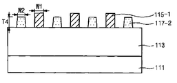
- FIG. 1 g shows the third hard mask pattern 117 - 2 having substantially the same width (w 2 ) as that of the first hard mask pattern 115 - 1 obtained by a second trimming etching process.
- the first trimming process is performed under O 2 of 1 ⁇ 2 sccm, CF 4 of 80 sccm and Ar of 50 sccm.
- the width W 2 of the third hard mask pattern 117 - 2 is substantially the same as W 1 of the first hard mask pattern 115 - 1 , and is formed apart from the first hard mask pattern at a given distance.
- the third hard mask pattern has the thickness of T 4 (0 ⁇ T 4 ⁇ T 3 ).
- FIG. 1 h shows the underlying layer pattern 113 - 1 obtained by a general etching process with the first and third hard mask patterns as etching masks.
- FIG. 1 i shows an underlying pattern 113 - 1 obtained by performing a subsequent cleaning process on the resulting structure to remove the first hard mask pattern 115 - 1 and the third hard mask 117 - 2 .
- the third hard mask pattern having a small pitch is formed between the first hard mask patterns by the double etching process including the first trimming process and the second trimming process. Therefore, when the underlying layer is etched using the first hard mask pattern and the third hard mask pattern as etching mask, a fine pattern is achieved that would otherwise cannot be obtained by a conventional lithography device.
- first hard mask film “second hard mask film,” “first hard mask pattern,” “second hard mask pattern,” and “third hard mask pattern” are used to describe the above embodiments. However, these are used for illustrative purposes.
- the present invention may be implemented using mask films (or mask patterns) that are not hard mask films (or hard mask patterns). Various alternatives and equivalents are possible.
- the invention is not limited by the lithography steps described herein. Nor is the invention limited to any specific type of semiconductor device.
- the present invention may be implemented in a dynamic random access memory (DRAM) device or non volatile memory device.
- DRAM dynamic random access memory
- Other additions, subtractions, or modifications are obvious in view of the present disclosure and are intended to fall within the scope of the appended claims.
Abstract
Description
Claims (21)
Applications Claiming Priority (4)
| Application Number | Priority Date | Filing Date | Title |
|---|---|---|---|
| KR20060018144 | 2006-02-24 | ||
| KR10-2006-0018144 | 2006-02-24 | ||
| KR1020060131936A KR100861212B1 (en) | 2006-02-24 | 2006-12-21 | Method for forming fine patterns of semiconductor devices |
| KR10-2006-0131936 | 2006-12-21 |
Publications (2)
| Publication Number | Publication Date |
|---|---|
| US20070202697A1 US20070202697A1 (en) | 2007-08-30 |
| US7745339B2 true US7745339B2 (en) | 2010-06-29 |
Family
ID=38444561
Family Applications (1)
| Application Number | Title | Priority Date | Filing Date |
|---|---|---|---|
| US11/672,676 Expired - Fee Related US7745339B2 (en) | 2006-02-24 | 2007-02-08 | Method for forming fine pattern of semiconductor device |
Country Status (1)
| Country | Link |
|---|---|
| US (1) | US7745339B2 (en) |
Cited By (1)
| Publication number | Priority date | Publication date | Assignee | Title |
|---|---|---|---|---|
| US8906757B2 (en) | 2011-12-06 | 2014-12-09 | Samsung Electronics Co., Ltd. | Methods of forming patterns of a semiconductor device |
Families Citing this family (24)
| Publication number | Priority date | Publication date | Assignee | Title |
|---|---|---|---|---|
| US8852851B2 (en) | 2006-07-10 | 2014-10-07 | Micron Technology, Inc. | Pitch reduction technology using alternating spacer depositions during the formation of a semiconductor device and systems including same |
| JP2009004535A (en) * | 2007-06-21 | 2009-01-08 | Toshiba Corp | Pattern forming method |
| JP4932671B2 (en) * | 2007-10-26 | 2012-05-16 | 東京エレクトロン株式会社 | Etching mask forming method, control program, and program storage medium |
| KR100942075B1 (en) * | 2007-12-27 | 2010-02-12 | 주식회사 하이닉스반도체 | Method of forming a micro pattern in a semiconductor device |
| JP5086283B2 (en) | 2008-02-15 | 2012-11-28 | 東京エレクトロン株式会社 | Pattern forming method and semiconductor device manufacturing method |
| JP5254049B2 (en) | 2008-02-15 | 2013-08-07 | 東京エレクトロン株式会社 | Pattern forming method and semiconductor device manufacturing method |
| US7989307B2 (en) | 2008-05-05 | 2011-08-02 | Micron Technology, Inc. | Methods of forming isolated active areas, trenches, and conductive lines in semiconductor structures and semiconductor structures including the same |
| US10151981B2 (en) * | 2008-05-22 | 2018-12-11 | Micron Technology, Inc. | Methods of forming structures supported by semiconductor substrates |
| US8039399B2 (en) * | 2008-10-09 | 2011-10-18 | Micron Technology, Inc. | Methods of forming patterns utilizing lithography and spacers |
| US8796155B2 (en) | 2008-12-04 | 2014-08-05 | Micron Technology, Inc. | Methods of fabricating substrates |
| US8273634B2 (en) | 2008-12-04 | 2012-09-25 | Micron Technology, Inc. | Methods of fabricating substrates |
| US8247302B2 (en) | 2008-12-04 | 2012-08-21 | Micron Technology, Inc. | Methods of fabricating substrates |
| US8268543B2 (en) | 2009-03-23 | 2012-09-18 | Micron Technology, Inc. | Methods of forming patterns on substrates |
| US9330934B2 (en) | 2009-05-18 | 2016-05-03 | Micron Technology, Inc. | Methods of forming patterns on substrates |
| US8518788B2 (en) | 2010-08-11 | 2013-08-27 | Micron Technology, Inc. | Methods of forming a plurality of capacitors |
| US8455341B2 (en) | 2010-09-02 | 2013-06-04 | Micron Technology, Inc. | Methods of forming features of integrated circuitry |
| US8575032B2 (en) | 2011-05-05 | 2013-11-05 | Micron Technology, Inc. | Methods of forming a pattern on a substrate |
| US9076680B2 (en) | 2011-10-18 | 2015-07-07 | Micron Technology, Inc. | Integrated circuitry, methods of forming capacitors, and methods of forming integrated circuitry comprising an array of capacitors and circuitry peripheral to the array |
| US8980757B2 (en) * | 2011-12-15 | 2015-03-17 | Intel Corporation | Methods for single exposure—self-aligned double, triple, and quadruple patterning |
| US9177794B2 (en) | 2012-01-13 | 2015-11-03 | Micron Technology, Inc. | Methods of patterning substrates |
| CN103377991B (en) * | 2012-04-18 | 2016-02-17 | 中芯国际集成电路制造(上海)有限公司 | The formation method of groove |
| US8629048B1 (en) | 2012-07-06 | 2014-01-14 | Micron Technology, Inc. | Methods of forming a pattern on a substrate |
| US20140054756A1 (en) * | 2012-08-23 | 2014-02-27 | Michael Hyatt | Anti spacer process and semiconductor structure generated by the anti spacer process |
| US10700072B2 (en) * | 2018-10-18 | 2020-06-30 | Applied Materials, Inc. | Cap layer for bit line resistance reduction |
Citations (22)
| Publication number | Priority date | Publication date | Assignee | Title |
|---|---|---|---|---|
| JPS54155771A (en) | 1978-05-29 | 1979-12-08 | Nec Corp | Pattern forming method |
| US4436583A (en) | 1981-12-21 | 1984-03-13 | Hitachi, Ltd. | Selective etching method of polyimide type resin film |
| US4863833A (en) | 1984-05-30 | 1989-09-05 | Fujitsu Limited | Pattern-forming material and its production and use |
| JPH02266517A (en) | 1989-04-06 | 1990-10-31 | Rohm Co Ltd | Manufacture of semiconductor device |
| KR930000130B1 (en) | 1989-08-22 | 1993-01-09 | 미쯔비시 덴끼 가부시끼가이샤 | Angle detecting apparatus |
| US5212043A (en) | 1988-02-17 | 1993-05-18 | Tosho Corporation | Photoresist composition comprising a non-aromatic resin having no aromatic structures derived from units of an aliphatic cyclic hydrocarbon and units of maleic anhydride and/or maleimide and a photosensitive agent |
| US5256248A (en) | 1991-10-10 | 1993-10-26 | Goldstar Electron Co., Ltd. | Method for patterning semiconductor |
| WO1996037526A1 (en) | 1995-05-25 | 1996-11-28 | The B.F. Goodrich Company | Addition polymers of polycycloolefins containing functional substituents |
| WO1997033198A1 (en) | 1996-03-07 | 1997-09-12 | The B.F. Goodrich Company | Photoresist compositions comprising polycyclic polymers with acid labile pendant groups |
| US5750680A (en) | 1995-09-14 | 1998-05-12 | Hyundai Electronics Industries Co., Ltd. | N-vinyllactam derivatives and polymer thereof |
| US6051678A (en) | 1996-12-20 | 2000-04-18 | Hyundai Electronics Industries Co., Ltd. | Copolymers containing N-vinyllactam derivatives, preparation methods thereof and photoresists therefrom |
| GB2345286A (en) | 1998-12-31 | 2000-07-05 | Hyundai Electronics Ind | Cross-linking monomers for photoresist, and process for preparing photoresist polymers using the same |
| US6132926A (en) | 1996-12-31 | 2000-10-17 | Hyundai Electronics Industries Co., Ltd. | ArF photoresist copolymers |
| US6225020B1 (en) | 1998-04-30 | 2001-05-01 | Hyundai Electronics Industries Co., Ltd. | Polymer and a forming method of a micro pattern using the same |
| US6235448B1 (en) | 1998-11-27 | 2001-05-22 | Hyundai Electronics Industries Co., Ltd. | Photoresist monomers, polymers thereof, and photoresist compositions containing the same |
| US6235447B1 (en) | 1998-10-17 | 2001-05-22 | Hyundai Electronics Industries Co., Ltd. | Photoresist monomers, polymers thereof, and photoresist compositions containing the same |
| JP2002319573A (en) | 2001-04-20 | 2002-10-31 | Toshiba Corp | Manufacturing method for semiconductor device |
| US6716761B2 (en) | 2001-01-16 | 2004-04-06 | Semiconductor Leading Edge Technologies, Inc. | Method of forming fine patterns |
| JP2004303870A (en) | 2003-03-31 | 2004-10-28 | Toshiba Corp | Method for forming fine pattern |
| KR20050052658A (en) | 2003-11-28 | 2005-06-03 | 삼성전자주식회사 | Method for forming fine patterns of semiconductor device |
| KR100694412B1 (en) | 2006-02-24 | 2007-03-12 | 주식회사 하이닉스반도체 | Method for forming fine patterns of semiconductor devices |
| KR100744683B1 (en) | 2006-02-27 | 2007-08-01 | 주식회사 하이닉스반도체 | Method for fabricating semiconductor device |
-
2007
- 2007-02-08 US US11/672,676 patent/US7745339B2/en not_active Expired - Fee Related
Patent Citations (22)
| Publication number | Priority date | Publication date | Assignee | Title |
|---|---|---|---|---|
| JPS54155771A (en) | 1978-05-29 | 1979-12-08 | Nec Corp | Pattern forming method |
| US4436583A (en) | 1981-12-21 | 1984-03-13 | Hitachi, Ltd. | Selective etching method of polyimide type resin film |
| US4863833A (en) | 1984-05-30 | 1989-09-05 | Fujitsu Limited | Pattern-forming material and its production and use |
| US5212043A (en) | 1988-02-17 | 1993-05-18 | Tosho Corporation | Photoresist composition comprising a non-aromatic resin having no aromatic structures derived from units of an aliphatic cyclic hydrocarbon and units of maleic anhydride and/or maleimide and a photosensitive agent |
| JPH02266517A (en) | 1989-04-06 | 1990-10-31 | Rohm Co Ltd | Manufacture of semiconductor device |
| KR930000130B1 (en) | 1989-08-22 | 1993-01-09 | 미쯔비시 덴끼 가부시끼가이샤 | Angle detecting apparatus |
| US5256248A (en) | 1991-10-10 | 1993-10-26 | Goldstar Electron Co., Ltd. | Method for patterning semiconductor |
| WO1996037526A1 (en) | 1995-05-25 | 1996-11-28 | The B.F. Goodrich Company | Addition polymers of polycycloolefins containing functional substituents |
| US5750680A (en) | 1995-09-14 | 1998-05-12 | Hyundai Electronics Industries Co., Ltd. | N-vinyllactam derivatives and polymer thereof |
| WO1997033198A1 (en) | 1996-03-07 | 1997-09-12 | The B.F. Goodrich Company | Photoresist compositions comprising polycyclic polymers with acid labile pendant groups |
| US6051678A (en) | 1996-12-20 | 2000-04-18 | Hyundai Electronics Industries Co., Ltd. | Copolymers containing N-vinyllactam derivatives, preparation methods thereof and photoresists therefrom |
| US6132926A (en) | 1996-12-31 | 2000-10-17 | Hyundai Electronics Industries Co., Ltd. | ArF photoresist copolymers |
| US6225020B1 (en) | 1998-04-30 | 2001-05-01 | Hyundai Electronics Industries Co., Ltd. | Polymer and a forming method of a micro pattern using the same |
| US6235447B1 (en) | 1998-10-17 | 2001-05-22 | Hyundai Electronics Industries Co., Ltd. | Photoresist monomers, polymers thereof, and photoresist compositions containing the same |
| US6235448B1 (en) | 1998-11-27 | 2001-05-22 | Hyundai Electronics Industries Co., Ltd. | Photoresist monomers, polymers thereof, and photoresist compositions containing the same |
| GB2345286A (en) | 1998-12-31 | 2000-07-05 | Hyundai Electronics Ind | Cross-linking monomers for photoresist, and process for preparing photoresist polymers using the same |
| US6716761B2 (en) | 2001-01-16 | 2004-04-06 | Semiconductor Leading Edge Technologies, Inc. | Method of forming fine patterns |
| JP2002319573A (en) | 2001-04-20 | 2002-10-31 | Toshiba Corp | Manufacturing method for semiconductor device |
| JP2004303870A (en) | 2003-03-31 | 2004-10-28 | Toshiba Corp | Method for forming fine pattern |
| KR20050052658A (en) | 2003-11-28 | 2005-06-03 | 삼성전자주식회사 | Method for forming fine patterns of semiconductor device |
| KR100694412B1 (en) | 2006-02-24 | 2007-03-12 | 주식회사 하이닉스반도체 | Method for forming fine patterns of semiconductor devices |
| KR100744683B1 (en) | 2006-02-27 | 2007-08-01 | 주식회사 하이닉스반도체 | Method for fabricating semiconductor device |
Non-Patent Citations (1)
| Title |
|---|
| Jung, Jae Chang, U.S. Appl. No. 11/672,680, filed Feb. 8, 2007 for "Method for Forming Fine Pattern of Semiconductor Device." |
Cited By (1)
| Publication number | Priority date | Publication date | Assignee | Title |
|---|---|---|---|---|
| US8906757B2 (en) | 2011-12-06 | 2014-12-09 | Samsung Electronics Co., Ltd. | Methods of forming patterns of a semiconductor device |
Also Published As
| Publication number | Publication date |
|---|---|
| US20070202697A1 (en) | 2007-08-30 |
Similar Documents
| Publication | Publication Date | Title |
|---|---|---|
| US7745339B2 (en) | Method for forming fine pattern of semiconductor device | |
| US7754591B2 (en) | Method for forming fine pattern of semiconductor device | |
| US7314810B2 (en) | Method for forming fine pattern of semiconductor device | |
| US7776750B2 (en) | Semiconductor device and method for forming a pattern in the same with double exposure technology | |
| US7651950B2 (en) | Method for forming a pattern of a semiconductor device | |
| US7935477B2 (en) | Double patterning strategy for contact hole and trench | |
| JP4901526B2 (en) | Method for forming fine pattern of semiconductor element and pattern forming method for substrate | |
| US8034544B2 (en) | Method for forming fine contact hole pattern of semiconductor device | |
| US7550384B2 (en) | Semiconductor device and method for forming pattern in the same | |
| KR100642886B1 (en) | Method of forming a micro pattern in a semiconductor device | |
| US20100112817A1 (en) | METHOD FOR FORMlNG PATTERN OF SEMICONDUCTOR DEVICE | |
| US20090170034A1 (en) | Method for manufacturing semiconductor device | |
| US7510973B2 (en) | Method for forming fine pattern in semiconductor device | |
| US20090298291A1 (en) | Method for forming a pattern of a semiconductor device | |
| JP5224919B2 (en) | Manufacturing method of semiconductor device | |
| US10734284B2 (en) | Method of self-aligned double patterning | |
| US7396751B2 (en) | Method for manufacturing semiconductor device | |
| US8304174B2 (en) | Method for fabricating semiconductor device | |
| US6680163B2 (en) | Method of forming opening in wafer layer | |
| US7718530B2 (en) | Method for manufacturing semiconductor device | |
| KR100894102B1 (en) | Method for fabricating highly integrated semiconductor memory device | |
| US8242021B2 (en) | Method for manufacturing semiconductor device | |
| TW201921123A (en) | Method of manufacturing semiconductor device | |
| US11515159B2 (en) | Forming contact holes using litho-etch-litho-etch approach | |
| KR101150492B1 (en) | Manufacturing method of semiconductor device using spacer patterning technology |
Legal Events
| Date | Code | Title | Description |
|---|---|---|---|
| AS | Assignment |
Owner name: HYNIX SEMICONDUCTOR INC.,KOREA, REPUBLIC OF Free format text: ASSIGNMENT OF ASSIGNORS INTEREST;ASSIGNOR:JUNG, JAE CHANG;REEL/FRAME:019051/0754 Effective date: 20070130 Owner name: HYNIX SEMICONDUCTOR INC., KOREA, REPUBLIC OF Free format text: ASSIGNMENT OF ASSIGNORS INTEREST;ASSIGNOR:JUNG, JAE CHANG;REEL/FRAME:019051/0754 Effective date: 20070130 |
|
| FEPP | Fee payment procedure |
Free format text: PAYOR NUMBER ASSIGNED (ORIGINAL EVENT CODE: ASPN); ENTITY STATUS OF PATENT OWNER: LARGE ENTITY |
|
| REMI | Maintenance fee reminder mailed | ||
| LAPS | Lapse for failure to pay maintenance fees | ||
| STCH | Information on status: patent discontinuation |
Free format text: PATENT EXPIRED DUE TO NONPAYMENT OF MAINTENANCE FEES UNDER 37 CFR 1.362 |
|
| FP | Lapsed due to failure to pay maintenance fee |
Effective date: 20140629 |