US7746720B2 - Techniques for reducing leakage current in memory devices - Google Patents

Techniques for reducing leakage current in memory devices Download PDF

Info

Publication number
US7746720B2
US7746720B2 US11/879,396 US87939607A US7746720B2 US 7746720 B2 US7746720 B2 US 7746720B2 US 87939607 A US87939607 A US 87939607A US 7746720 B2 US7746720 B2 US 7746720B2
Authority
US
United States
Prior art keywords
word lines
voltage level
voltage
memory array
section
Prior art date
Legal status (The legal status is an assumption and is not a legal conclusion. Google has not performed a legal analysis and makes no representation as to the accuracy of the status listed.)
Active, expires
Application number
US11/879,396
Other versions
US20070263470A1 (en
Inventor
Scott J. Derner
Venkatraghavan Bringivijayaraghavan
Abhay S. Dixit
Scot M. Graham
Stephen R. Porter
Ethan A. Williford
Current Assignee (The listed assignees may be inaccurate. Google has not performed a legal analysis and makes no representation or warranty as to the accuracy of the list.)
US Bank NA
Original Assignee
Micron Technology Inc
Priority date (The priority date is an assumption and is not a legal conclusion. Google has not performed a legal analysis and makes no representation as to the accuracy of the date listed.)
Filing date
Publication date
Application filed by Micron Technology Inc filed Critical Micron Technology Inc
Priority to US11/879,396 priority Critical patent/US7746720B2/en
Publication of US20070263470A1 publication Critical patent/US20070263470A1/en
Application granted granted Critical
Publication of US7746720B2 publication Critical patent/US7746720B2/en
Assigned to U.S. BANK NATIONAL ASSOCIATION, AS COLLATERAL AGENT reassignment U.S. BANK NATIONAL ASSOCIATION, AS COLLATERAL AGENT SECURITY INTEREST (SEE DOCUMENT FOR DETAILS). Assignors: MICRON TECHNOLOGY, INC.
Assigned to MORGAN STANLEY SENIOR FUNDING, INC., AS COLLATERAL AGENT reassignment MORGAN STANLEY SENIOR FUNDING, INC., AS COLLATERAL AGENT PATENT SECURITY AGREEMENT Assignors: MICRON TECHNOLOGY, INC.
Assigned to U.S. BANK NATIONAL ASSOCIATION, AS COLLATERAL AGENT reassignment U.S. BANK NATIONAL ASSOCIATION, AS COLLATERAL AGENT CORRECTIVE ASSIGNMENT TO CORRECT THE REPLACE ERRONEOUSLY FILED PATENT #7358718 WITH THE CORRECT PATENT #7358178 PREVIOUSLY RECORDED ON REEL 038669 FRAME 0001. ASSIGNOR(S) HEREBY CONFIRMS THE SECURITY INTEREST. Assignors: MICRON TECHNOLOGY, INC.
Assigned to JPMORGAN CHASE BANK, N.A., AS COLLATERAL AGENT reassignment JPMORGAN CHASE BANK, N.A., AS COLLATERAL AGENT SECURITY INTEREST (SEE DOCUMENT FOR DETAILS). Assignors: MICRON SEMICONDUCTOR PRODUCTS, INC., MICRON TECHNOLOGY, INC.
Assigned to MICRON TECHNOLOGY, INC. reassignment MICRON TECHNOLOGY, INC. RELEASE BY SECURED PARTY (SEE DOCUMENT FOR DETAILS). Assignors: U.S. BANK NATIONAL ASSOCIATION, AS COLLATERAL AGENT
Assigned to MICRON TECHNOLOGY, INC. reassignment MICRON TECHNOLOGY, INC. RELEASE BY SECURED PARTY (SEE DOCUMENT FOR DETAILS). Assignors: MORGAN STANLEY SENIOR FUNDING, INC., AS COLLATERAL AGENT
Assigned to MICRON SEMICONDUCTOR PRODUCTS, INC., MICRON TECHNOLOGY, INC. reassignment MICRON SEMICONDUCTOR PRODUCTS, INC. RELEASE BY SECURED PARTY (SEE DOCUMENT FOR DETAILS). Assignors: JPMORGAN CHASE BANK, N.A., AS COLLATERAL AGENT
Active legal-status Critical Current
Adjusted expiration legal-status Critical

Links

Images

Classifications

    • GPHYSICS
    • G11INFORMATION STORAGE
    • G11CSTATIC STORES
    • G11C11/00Digital stores characterised by the use of particular electric or magnetic storage elements; Storage elements therefor
    • G11C11/21Digital stores characterised by the use of particular electric or magnetic storage elements; Storage elements therefor using electric elements
    • G11C11/34Digital stores characterised by the use of particular electric or magnetic storage elements; Storage elements therefor using electric elements using semiconductor devices
    • G11C11/40Digital stores characterised by the use of particular electric or magnetic storage elements; Storage elements therefor using electric elements using semiconductor devices using transistors
    • G11C11/41Digital stores characterised by the use of particular electric or magnetic storage elements; Storage elements therefor using electric elements using semiconductor devices using transistors forming static cells with positive feedback, i.e. cells not needing refreshing or charge regeneration, e.g. bistable multivibrator or Schmitt trigger
    • G11C11/412Digital stores characterised by the use of particular electric or magnetic storage elements; Storage elements therefor using electric elements using semiconductor devices using transistors forming static cells with positive feedback, i.e. cells not needing refreshing or charge regeneration, e.g. bistable multivibrator or Schmitt trigger using field-effect transistors only
    • GPHYSICS
    • G11INFORMATION STORAGE
    • G11CSTATIC STORES
    • G11C11/00Digital stores characterised by the use of particular electric or magnetic storage elements; Storage elements therefor
    • G11C11/21Digital stores characterised by the use of particular electric or magnetic storage elements; Storage elements therefor using electric elements
    • G11C11/34Digital stores characterised by the use of particular electric or magnetic storage elements; Storage elements therefor using electric elements using semiconductor devices
    • G11C11/40Digital stores characterised by the use of particular electric or magnetic storage elements; Storage elements therefor using electric elements using semiconductor devices using transistors
    • G11C11/401Digital stores characterised by the use of particular electric or magnetic storage elements; Storage elements therefor using electric elements using semiconductor devices using transistors forming cells needing refreshing or charge regeneration, i.e. dynamic cells
    • G11C11/4063Auxiliary circuits, e.g. for addressing, decoding, driving, writing, sensing or timing
    • G11C11/407Auxiliary circuits, e.g. for addressing, decoding, driving, writing, sensing or timing for memory cells of the field-effect type
    • G11C11/408Address circuits
    • G11C11/4085Word line control circuits, e.g. word line drivers, - boosters, - pull-up, - pull-down, - precharge

Definitions

  • the present invention relates generally to memory devices and, more particularly, to techniques for reducing leakage current in memory devices.
  • CMOS complementary metal oxide semiconductor
  • SRAM static random access memory
  • DRAM dynamic random access memory
  • S VT CMOS sub-threshold leakage
  • GIDL gate induced drain leakage
  • Sub-threshold leakage refers generally to the leakage current through the channel of a CMOS transistor.
  • CMOS transistor For a one-transistor, one-capacitor (1T-1C) dynamic random access (DRAM) memory cell, for instance, leakage from the charge stored in the capacitor may occur through the channel.
  • One technique for reducing the sub-threshold leakage in a CMOS transistor is to implant the channel with an impurity, such as boron for a n-channel device. By implanting boron in the channel directly below the gate and directly adjacent to the drain, the threshold voltage (V T ) across the gate is increased, thereby lowering the sub-threshold leakage.
  • V T threshold voltage
  • the increased doping in the channel disadvantageously increases the junction leakage between the n+ doped drain region and the p-type substrate material.
  • Gate induced drain leakage is generally caused by a high gate to drain electric field in the region of the gate that overlaps the drain. As device size decreases and the thickness of the gate oxide is reduced, GIDL currents increasingly impact the total off current of the device.
  • Techniques for reducing GIDL are primarily implemented by introducing CMOS design level modifications. For instance, one approach for reducing GIDL currents involves symmetrical oxidation to provide a thin gate oxide through the channel of the device, but to provide a thicker gate oxide in the regions of the gate-source and gate-drain overlap. The thick gate oxide in the gate-drain region reduces the GIDL. However, having a thick gate oxide in the gate-source region increases the V T which generally reduces current driving capabilities of the device. Another approach to reducing GIDL currents is asymmetrical oxidation such that the gate oxide is thicker only in the gate-drain region.
  • the present invention may address one or more of the problems set forth above.
  • FIG. 1 illustrates a block diagram of an exemplary processor-based device
  • FIG. 2 illustrates a block diagram of an exemplary memory device that may be configured in accordance with the present techniques
  • FIG. 3 illustrates a block diagram of an exemplary memory array in the memory device of FIG. 2 that may be configured in accordance with the present techniques
  • FIG. 4 illustrates a partial cross-sectional view, partial schematic of an exemplary memory cell in the memory array of FIG. 3 that may be configured in accordance with the present techniques
  • FIG. 5 illustrates a schematic diagram of an exemplary embodiment of a portion of a row driver block for improving gate induced drain leakage (GIDL), in accordance with embodiments of the present techniques.
  • GIDL gate induced drain leakage
  • FIG. 1 a block diagram depicting an exemplary processor-based system, generally designated by reference numeral 10 , is illustrated.
  • the system 10 may be any of a variety of types such as a computer, pager, cellular phone, personal organizer, control circuit, etc.
  • a processor 12 such as a microprocessor, controls the processing of system functions and requests in the system 10 .
  • the processor 12 may comprise a plurality of processors that share system control.
  • the system 10 typically includes a power supply 14 .
  • the power supply 14 may advantageously include permanent batteries, replaceable batteries, and/or rechargeable batteries.
  • the power supply 14 may also include an AC adapter, so the system 10 may be plugged into a wall outlet, for instance.
  • the power supply 14 may also include a DC adapter such that the system 10 maybe plugged into a vehicle cigarette lighter, for instance.
  • a user interface 16 may be coupled to the processor 12 .
  • the user interface 16 may include buttons, switches, a keyboard, a light pen, a mouse, and/or a voice recognition system, for instance.
  • a display 18 may also be coupled to the processor 12 .
  • the display 18 may include an LCD display, a CRT, LEDs, and/or an audio display, for example.
  • an RF sub-system/baseband processor 20 may also be couple to the processor 12 .
  • the RF sub-system/baseband processor 20 may include an antenna that is coupled to an RF receiver and to an RF transmitter (not shown).
  • a communications port 22 may also be coupled to the processor 12 .
  • the communications port 22 may be adapted to be coupled to one or more peripheral devices 24 such as a modem, a printer, a computer, or to a network, such as a local area network, remote area network, intranet, or the Internet, for instance.
  • the processor 12 controls the functioning of the system 10 by implementing 20 software programs, memory is used to enable the processor 12 to be efficient.
  • the memory is coupled to the processor 12 to store and facilitate execution of various programs.
  • the processor 12 may be coupled to the volatile memory 26 which may include Dynamic Random Access Memory (DRAM) and/or Static Random Access Memory (SRAM).
  • the processor 12 may also be coupled to non-volatile memory 28 .
  • the non-volatile memory 28 may include a read-only memory (ROM), such as an EPROM, and/or flash memory to be used in conjunction with the volatile memory.
  • ROM read-only memory
  • the size of the ROM is typically selected to be just large enough to store any necessary operating system, application programs, and fixed data.
  • the volatile memory 26 on the other hand, is typically quite large so that it can store dynamically loaded applications and data.
  • the non-volatile memory 28 may include a high capacity memory such as a tape or disk drive memory.
  • FIG. 2 is a block diagram illustrating a memory device 30 that may be implemented in the volatile memory 26 of FIG. 1 .
  • the memory device 30 generally includes a memory array 32 .
  • the memory array 32 generally includes many rows and columns of conductive traces arranged in a grid pattern to form a number of memory cells.
  • the rows or “row lines” that make up the memory array 32 are generally referred to as “wordlines.”
  • the columns or “column lines” are generally referred to as “bit lines” or “digit lines.” Each column may actually comprise a pair of complimentary bit lines, as will be further illustrated with respect to FIG. 3 .
  • the memory array 32 may include a number of sub arrays or sections 34 . In one embodiment, 64 sub arrays or sections 34 , each having 512 rows and columns may be used to form a 16 Mb array. As will be appreciated, four of the 16 Mb arrays may be combined to form a 64 Mb DRAM, for instance.
  • a row decoder block 36 and a column decoder block 37 are provided and are configured to receive and translate address information from the processor 12 via the address bus 38 to access a particular memory cell in the memory array 32 .
  • a sense amplifier block 40 having a plurality of the sense amplifies (one sense amplifier for each bit line pair, for example) is also provided between the column decoder 37 and the memory array 32 to sense and amplify individual values stored in the memory cells.
  • a row driver block 42 is provided between the row decoder block 36 and the memory array 32 to activate a selected word lines in the memory array according to a given row address.
  • the row driver block 42 may be configured such that gate induced drain leakage (GIDL) is advantageously reduced, as further described below with reference to FIGS. 3 and 4 .
  • GIDL gate induced drain leakage
  • data may be transferred to and from the memory device 30 via the data bus 44 .
  • the data bus 44 may be a 16-bit data bus configured to carry data at 400 MHz, for example.
  • the coordination of the data and address information may be conducted through a data control circuit block 46 .
  • the memory device 30 may include a control circuit 48 configured to receive control signals from the processor 12 via the control bus 50 .
  • the control circuit 48 is coupled to each of the row decoder block 36 , the column decoder block 37 , the sense amplifier block 40 , the row driver block 42 and the data control circuit block 46 , and is generally configured to coordinate timing and control among the various circuits in the memory device 30 .
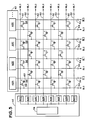
  • FIG. 3 illustrates a portion of a sub array or section 34 of the memory array 32 .
  • the section 34 of the memory array 32 includes a number of word lines 52 and a number of complimentary bit lines 54 .
  • the bit lines 54 are generally arranged such that complimentary bit line pairs are coupled to a respective sense amplifier in the sense amplifier block 40 .
  • complimentary bit line pairs BL 0 and BL 0 are coupled to the sense amplifier 40 A.
  • Complementary bit lines BL 1 and BL 1 are coupled to the sense amplifier 40 B.
  • Bit line pairs BL 2 and BL 2 are coupled to the sense amplifier 40 C, and bit line pairs BL 3 and BL 3 are coupled to the sense amplifier 40 D.
  • each memory cell 56 may include an access device, such as a transistor 58 , and a storage device, such as a capacitor 60 .
  • the transistor 58 of the memory cell 56 may be a metal-oxide semiconductor field effect transistor (MOSFET), complementary metal-oxide-semiconductor transistor (CMOS) or any other suitable transistor. Further, the transistor 58 may be an n-channel or a p-channel device, depending on the specific design.
  • MOSFET metal-oxide semiconductor field effect transistor
  • CMOS complementary metal-oxide-semiconductor transistor
  • the drain terminal of the transistor 58 is connected to one terminal of the capacitor 60 .
  • the source terminal of the transistor 58 is coupled to a bit line 54 .
  • the source and drain terminals may be reversed.
  • the gate of the transistor 58 is coupled to a respective word line 52 .
  • a first voltage is applied to the word line 52 and to the gate of the transistor 58 .
  • the voltage applied to the gate of the transistor 58 opens the transistor to allow a second voltage applied to a bit line 54 to flow through the transistor 58 and into the capacitor 60 .
  • the capacitor 60 stores the charge that was applied to the bit line 54 when a voltage is applied to the word line 52 to open the gate of the transistor 58 , as will be appreciated by those skilled in the art.
  • the memory cell 56 may be fabricated on a p-type substrate 62 , having n+ doped regions which form the drain terminal 64 and the source terminal 66 of the transistor 58 (illustrated in FIG. 4 by dashed lines).
  • the word line 52 is configured to form the gate 68 of the transistor 58 .
  • the gate 68 includes a conductive layer 70 and a gate oxide layer 72 .
  • the source terminal 66 is coupled to a bit line 54
  • the drain terminal 64 is coupled to the capacitor 60 .
  • boron (or any other suitable p-type impurity) is often implanted in the substrate 62 , directly below the gate oxide layer 72 and adjacent to the drain terminal 64 . While the addition of boron may improve the sub-threshold leakage, it negatively impacts (increases) the junction leakage. In considering the amount of boron to add to the substrate, the tradeoffs between the sub-threshold leakage and the junction leakage become relevant.
  • One such technique to allow an acceptable amount of sub-threshold leakage and junction leakage is to reduce the boron concentration in the channel and compensate for the increased sub-threshold leakage by taking the gate to drain potential of the transistor negative.
  • To increase the voltage potential across the drain-gate more electron-hole pairs are created, thereby providing a stronger E field (indicated by electric field lines 74 in FIG. 4 ) between the drain terminal 64 and the gate 68 .
  • the word line 52 may be driven to a negative voltage, such as ⁇ 0.3 volts, rather than to ground.
  • an improved row driver block 42 for reducing the GIDL 76 in memory devices implementing negative word lines architectures is provided.
  • the row driver block 42 includes a voltage selection circuit 78 which is configured to selectably couple any of the word lines 52 to either of a first voltage level, such as a negative voltage level, or a second voltage level, such as ground, when each of the word lines 52 in the memory section or sub array 34 is inactive.
  • the negative voltage level may be ⁇ 0.3 volts, for example.
  • the row driver block 42 may also include a level translator 80 A- 80 H, wherein each word line 52 includes a corresponding level translator 80 A- 80 H.
  • a word line 52 in the sub array 34 is active, such as during ACT mode or long RAS mode, all of the inactive word lines 52 are coupled to the negative word line voltage.
  • the row driver block 42 includes a voltage selection circuit 78 for each section 34 of the memory array 32 and a plurality of level translators (e.g., 80 A- 80 C), wherein each of the word lines (e.g., WL 0 -WL 2 ) is coupled to a corresponding level translator.
  • the memory section 34 FIG. 2
  • the level translators 80 A- 80 C may be omitted.
  • each level translator 80 A- 80 C comprises a corresponding pair of p-channel and n-channel transistors, 82 A- 82 C and 84 A- 84 C, respectively.
  • Each p-channel transistor 82 A- 82 C is coupled to a positive voltage source V CCP which enables the active mode on the respective word line WL 0 -WL 2 .
  • V CCP is generally about 1.5 volts higher than V CC .
  • V CC is equal to approximately 2.0 volts and V CCP is approximately equal to 3.5 volts.
  • the voltage selection circuit 78 receives a section signal SEC, which is implemented to indicate whether any of the word lines WL 0 -WL 2 in the corresponding section 34 of the memory array 32 are active.
  • the voltage selection circuit 78 is configured to drive each of the inactive word lines WL 0 -WL 2 to V NEGWL .
  • V NEGWL is approximately equal to ⁇ 0.3 volts.
  • the present exemplary embodiment of the voltage selection circuit 78 includes a pull-down transistor 86 , coupled between the common node 88 and ground and a pull-down transistor 90 , coupled between the common node 88 and the negative word line voltage V NEGWL .
  • the gate of the pull-down transistor 86 receives the inverse of the section signal SEC through the inverter 91 .
  • the voltage selection circuit 78 also includes a voltage translator 92 coupled between the positive voltage V CC (e.g., 2.0 volts) and a negative substrate voltage V BB (e.g., ⁇ 1.0 volts).
  • the voltage translator 92 includes a pair of p-channel transistors 94 and 96 , a pair of n-channel transistors 98 and 100 and an inverter 102 .
  • the voltage translator 92 is configured to convert ground to the negative substrate voltage V BB . If the input of the voltage translator 92 receives V CC , the output of the voltage translator 92 , which is coupled to the gate of the pull-down transistor 90 , receives the voltage V CC . If the input of the voltage translator 92 is grounded, the output of the voltage translator 92 is the negative substrate voltage V BB .
  • the section signal SEC is used to determine whether the inactive word lines WL 0 -WL 2 in the section 34 are to be coupled to ground (through the pull-down transistor 86 ) or to the negative word line voltage V NEGWL through the pull-down resistor 90 ). If the section signal SEC is enabled (high), then one of the word lines WL 0 -WL 2 in the section 34 is active and the inactive word lines WL 0 -WL 2 in the section 34 are coupled to the negative word line voltage V NEGWL . If the section signal SEC is disabled (low), then all of the word lines WL 0 -WL 2 in the section 34 are inactive and all of the word lines WL 0 -WL 2 in the section 34 are coupled to ground.

Abstract

Techniques for reducing gate induced drain leakage (GIDL) in memory devices utilizing negative wordline architectures. More specifically, a method and apparatus are provided to determine whether any of the word lines in a section of a memory array are active. If any one of the plurality of word lines is active, each of the inactive word lines in the section are coupled to a negative voltage level. If none of the plurality of word lines is active, each of the plurality of word lines is coupled to ground to reduce GIDL.

Description

CROSS REFERENCE TO RELATED APPLICATIONS
The present application is a continuation of and claims priority to U.S. patent application Ser. No. 10/900,246, filed Jul. 27, 2004, now U.S. Pat. No. 7,245,548, which issued on Jul. 17, 2007.
BACKGROUND OF THE INVENTION
1. Field of the Invention
The present invention relates generally to memory devices and, more particularly, to techniques for reducing leakage current in memory devices.
2. Description of the Related Art
This section is intended to introduce the reader to various aspects of art which may be related to various aspects of the present invention which are described and/or claimed below. This discussion is believed to be helpful in providing the reader with background information to facilitate a better understanding of the various aspects of the present invention. Accordingly, it should be understood that these statements are to be read in this light, and not as admissions of prior art.
In recent years, the minimization of structural dimensions in integrated circuit devices, such as memory devices fabricated using complementary metal oxide semiconductor (CMOS) technology, have led to ever-increasing sub-threshold leakage currents in the devices. The leakage current is typically produced from inherent qualities associated with the CMOS technology that is typically used to manufacture static random access memory (SRAM) and dynamic random access memory (DRAM) devices. CMOS sub-threshold leakage (SVT), junction leakage and gate induced drain leakage (GIDL) in the memory core may negatively impact device performance. To date, most leakage mechanism techniques focus on sub-threshold leakage reduction and junction leakage, without considering the effects of gate induced leakage, since sub-threshold leakage and junction leakage are generally of greater impact on device performance.
Sub-threshold leakage refers generally to the leakage current through the channel of a CMOS transistor. For a one-transistor, one-capacitor (1T-1C) dynamic random access (DRAM) memory cell, for instance, leakage from the charge stored in the capacitor may occur through the channel. One technique for reducing the sub-threshold leakage in a CMOS transistor, is to implant the channel with an impurity, such as boron for a n-channel device. By implanting boron in the channel directly below the gate and directly adjacent to the drain, the threshold voltage (VT) across the gate is increased, thereby lowering the sub-threshold leakage. However, while increasing the threshold voltage may advantageously decrease the sub-threshold leakage, the increased doping in the channel disadvantageously increases the junction leakage between the n+ doped drain region and the p-type substrate material.
Gate induced drain leakage (GIDL) is generally caused by a high gate to drain electric field in the region of the gate that overlaps the drain. As device size decreases and the thickness of the gate oxide is reduced, GIDL currents increasingly impact the total off current of the device.
Techniques for reducing GIDL are primarily implemented by introducing CMOS design level modifications. For instance, one approach for reducing GIDL currents involves symmetrical oxidation to provide a thin gate oxide through the channel of the device, but to provide a thicker gate oxide in the regions of the gate-source and gate-drain overlap. The thick gate oxide in the gate-drain region reduces the GIDL. However, having a thick gate oxide in the gate-source region increases the VT which generally reduces current driving capabilities of the device. Another approach to reducing GIDL currents is asymmetrical oxidation such that the gate oxide is thicker only in the gate-drain region. The material thickness of the oxide layer in gate-drain region is increased by implanting an oxidation accelerating material, such as chlorine or fluorine to physically grow a thicker gate oxide layer in that particular region. Due to the presence of the oxidation accelerating material, the oxide layer in the gate-drain region grows faster than in the remaining portions of the substrate. However, as with the symmetrical oxidation, having an increased material thickness of the oxide layer in the gate-drain region dampers current driving capability of the device and also causes increased stress in the active area near the overlap region due to the volume expansion.
Further, implementing structural changes to the design of the device layers may introduce other variables that may ultimately negatively impact device performance. Implementing such changes may also be impractical in current manufacturing facilities.
The present invention may address one or more of the problems set forth above.
BRIEF DESCRIPTION OF THE DRAWINGS
The foregoing and other advantages of the invention may become apparent upon reading the following detailed description and upon reference to the drawings in which:
FIG. 1 illustrates a block diagram of an exemplary processor-based device;
FIG. 2 illustrates a block diagram of an exemplary memory device that may be configured in accordance with the present techniques;
FIG. 3 illustrates a block diagram of an exemplary memory array in the memory device of FIG. 2 that may be configured in accordance with the present techniques;
FIG. 4 illustrates a partial cross-sectional view, partial schematic of an exemplary memory cell in the memory array of FIG. 3 that may be configured in accordance with the present techniques; and
FIG. 5 illustrates a schematic diagram of an exemplary embodiment of a portion of a row driver block for improving gate induced drain leakage (GIDL), in accordance with embodiments of the present techniques.
DETAILED DESCRIPTION OF SPECIFIC EMBODIMENTS
One or more specific embodiments of the present invention will be described below. In an effort to provide a concise description of these embodiments, not all features of an actual implementation are described in the specification. It should be appreciated that in the development of any such actual implementation, as in any engineering or design project, numerous implementation-specific decisions must be made to achieve the developers' specific goals, such as compliance with system-related and business-related constraints, which may vary from one implementation to another. Moreover, it should be appreciated that such a development effort might be complex and time consuming, but would nevertheless be a routine undertaking of design, fabrication, and manufacture for those of ordinary skill having the benefit of this disclosure.
Turning now to the drawings, and referring initially to FIG. 1, a block diagram depicting an exemplary processor-based system, generally designated by reference numeral 10, is illustrated. The system 10 may be any of a variety of types such as a computer, pager, cellular phone, personal organizer, control circuit, etc. In a typical processor-based device, a processor 12, such as a microprocessor, controls the processing of system functions and requests in the system 10. Further, the processor 12 may comprise a plurality of processors that share system control.
The system 10 typically includes a power supply 14. For instance, if the system 10 is a portable system, the power supply 14 may advantageously include permanent batteries, replaceable batteries, and/or rechargeable batteries. The power supply 14 may also include an AC adapter, so the system 10 may be plugged into a wall outlet, for instance. The power supply 14 may also include a DC adapter such that the system 10 maybe plugged into a vehicle cigarette lighter, for instance.
Various other devices may be coupled to the processor 12 depending on the functions that the system 10 performs. For instance, a user interface 16 may be coupled to the processor 12. The user interface 16 may include buttons, switches, a keyboard, a light pen, a mouse, and/or a voice recognition system, for instance. A display 18 may also be coupled to the processor 12. The display 18 may include an LCD display, a CRT, LEDs, and/or an audio display, for example.
Furthermore, an RF sub-system/baseband processor 20 may also be couple to the processor 12. The RF sub-system/baseband processor 20 may include an antenna that is coupled to an RF receiver and to an RF transmitter (not shown). A communications port 22 may also be coupled to the processor 12. The communications port 22 may be adapted to be coupled to one or more peripheral devices 24 such as a modem, a printer, a computer, or to a network, such as a local area network, remote area network, intranet, or the Internet, for instance.
Because the processor 12 controls the functioning of the system 10 by implementing 20 software programs, memory is used to enable the processor 12 to be efficient. Generally, the memory is coupled to the processor 12 to store and facilitate execution of various programs. For instance, the processor 12 may be coupled to the volatile memory 26 which may include Dynamic Random Access Memory (DRAM) and/or Static Random Access Memory (SRAM). The processor 12 may also be coupled to non-volatile memory 28. The non-volatile memory 28 may include a read-only memory (ROM), such as an EPROM, and/or flash memory to be used in conjunction with the volatile memory. The size of the ROM is typically selected to be just large enough to store any necessary operating system, application programs, and fixed data. The volatile memory 26 on the other hand, is typically quite large so that it can store dynamically loaded applications and data. Additionally, the non-volatile memory 28 may include a high capacity memory such as a tape or disk drive memory.
FIG. 2 is a block diagram illustrating a memory device 30 that may be implemented in the volatile memory 26 of FIG. 1. The memory device 30 generally includes a memory array 32. The memory array 32 generally includes many rows and columns of conductive traces arranged in a grid pattern to form a number of memory cells. The rows or “row lines” that make up the memory array 32 are generally referred to as “wordlines.” The columns or “column lines” are generally referred to as “bit lines” or “digit lines.” Each column may actually comprise a pair of complimentary bit lines, as will be further illustrated with respect to FIG. 3. As described further below, the memory array 32 may include a number of sub arrays or sections 34. In one embodiment, 64 sub arrays or sections 34, each having 512 rows and columns may be used to form a 16 Mb array. As will be appreciated, four of the 16 Mb arrays may be combined to form a 64 Mb DRAM, for instance.
To access the memory array 32, a row decoder block 36 and a column decoder block 37 are provided and are configured to receive and translate address information from the processor 12 via the address bus 38 to access a particular memory cell in the memory array 32. A sense amplifier block 40 having a plurality of the sense amplifies (one sense amplifier for each bit line pair, for example) is also provided between the column decoder 37 and the memory array 32 to sense and amplify individual values stored in the memory cells. Further, a row driver block 42 is provided between the row decoder block 36 and the memory array 32 to activate a selected word lines in the memory array according to a given row address. In accordance with embodiments of the present invention, the row driver block 42 may be configured such that gate induced drain leakage (GIDL) is advantageously reduced, as further described below with reference to FIGS. 3 and 4.
During read and write operations, data may be transferred to and from the memory device 30 via the data bus 44. The data bus 44 may be a 16-bit data bus configured to carry data at 400 MHz, for example. The coordination of the data and address information may be conducted through a data control circuit block 46. Finally, the memory device 30 may include a control circuit 48 configured to receive control signals from the processor 12 via the control bus 50. The control circuit 48 is coupled to each of the row decoder block 36, the column decoder block 37, the sense amplifier block 40, the row driver block 42 and the data control circuit block 46, and is generally configured to coordinate timing and control among the various circuits in the memory device 30.
Referring now to FIG. 3, a portion of a sub array or section 34 of the memory array 32 is illustrated. In particular, FIG. 3 illustrates a portion of a dynamic random access memory (DRAM) array. As previously described, the section 34 of the memory array 32 includes a number of word lines 52 and a number of complimentary bit lines 54. The bit lines 54 are generally arranged such that complimentary bit line pairs are coupled to a respective sense amplifier in the sense amplifier block 40. Specifically in the portion of the section 34 of the memory array 32 illustrated in FIG. 3, complimentary bit line pairs BL0 and BL0 are coupled to the sense amplifier 40A. Complementary bit lines BL1 and BL1 are coupled to the sense amplifier 40B. Bit line pairs BL2 and BL2 are coupled to the sense amplifier 40C, and bit line pairs BL3 and BL3 are coupled to the sense amplifier 40D.
As previously described, the word lines 52 and the bit lines 54 are arranged in a grid pattern to provide an array of individual memory cells 56. Each memory cell 56 may include an access device, such as a transistor 58, and a storage device, such as a capacitor 60. The transistor 58 of the memory cell 56 may be a metal-oxide semiconductor field effect transistor (MOSFET), complementary metal-oxide-semiconductor transistor (CMOS) or any other suitable transistor. Further, the transistor 58 may be an n-channel or a p-channel device, depending on the specific design.
The drain terminal of the transistor 58 is connected to one terminal of the capacitor 60. The source terminal of the transistor 58 is coupled to a bit line 54. As will be appreciated, depending on the mode of operation of the transistor 58, the source and drain terminals may be reversed. The gate of the transistor 58 is coupled to a respective word line 52.
To store information in a memory cell 56, via an electrical charge, a first voltage is applied to the word line 52 and to the gate of the transistor 58. The voltage applied to the gate of the transistor 58 opens the transistor to allow a second voltage applied to a bit line 54 to flow through the transistor 58 and into the capacitor 60. Accordingly, the capacitor 60 stores the charge that was applied to the bit line 54 when a voltage is applied to the word line 52 to open the gate of the transistor 58, as will be appreciated by those skilled in the art.
Referring briefly to FIG. 4, a partial cross-sectional view, partial schematic of the memory cell 56 is illustrated. The memory cell 56 may be fabricated on a p-type substrate 62, having n+ doped regions which form the drain terminal 64 and the source terminal 66 of the transistor 58 (illustrated in FIG. 4 by dashed lines). As will be appreciated, the word line 52 is configured to form the gate 68 of the transistor 58. The gate 68 includes a conductive layer 70 and a gate oxide layer 72. The source terminal 66 is coupled to a bit line 54, and the drain terminal 64 is coupled to the capacitor 60.
As previously described, to improve the sub-threshold leakage, boron (or any other suitable p-type impurity) is often implanted in the substrate 62, directly below the gate oxide layer 72 and adjacent to the drain terminal 64. While the addition of boron may improve the sub-threshold leakage, it negatively impacts (increases) the junction leakage. In considering the amount of boron to add to the substrate, the tradeoffs between the sub-threshold leakage and the junction leakage become relevant.
One such technique to allow an acceptable amount of sub-threshold leakage and junction leakage is to reduce the boron concentration in the channel and compensate for the increased sub-threshold leakage by taking the gate to drain potential of the transistor negative. To increase the voltage potential across the drain-gate, more electron-hole pairs are created, thereby providing a stronger E field (indicated by electric field lines 74 in FIG. 4) between the drain terminal 64 and the gate 68. To increase the voltage potential between the drain terminal 64 and the gate 68 when the word line 52 is off, the word line 52 may be driven to a negative voltage, such as −0.3 volts, rather than to ground. By driving the gate 68 to a negative voltage, the E-field 74 is increased and the voltage potential across the drain-gate is increased. While this provides desirable effects in reducing the sub-threshold leakage while the word line 52 is inactive, it disadvantageously increases the GIDL, generally indicated by reference numeral 76. In accordance with embodiments of the present invention, an improved row driver block 42 for reducing the GIDL 76 in memory devices implementing negative word lines architectures is provided.
Referring again to FIG. 3, a block diagram of the row driver block 42, in accordance with embodiments of the present invention, is generally illustrated. A schematic diagram illustrating an exemplary embodiment will be described further below with reference to FIG. 5. Generally, the row driver block 42 includes a voltage selection circuit 78 which is configured to selectably couple any of the word lines 52 to either of a first voltage level, such as a negative voltage level, or a second voltage level, such as ground, when each of the word lines 52 in the memory section or sub array 34 is inactive. The negative voltage level may be −0.3 volts, for example. The row driver block 42 may also include a level translator 80A-80H, wherein each word line 52 includes a corresponding level translator 80A-80H.
By coupling all of the word lines 52 in a sub array 34 to ground, rather than a negative voltage, when all of the word lines are inactive, such as in a standby mode or a static refresh mode, for example, the GIDL effect that the off word lines have on the storage node is alleviated and the refresh performance is improved. Sub-threshold leakage is of less concern when each of the word lines 52 is inactive, because the inactive transistors only have a VCC/2 voltage stress across the source to drain junction.
In contrast, if a word line 52 in the sub array 34 is active, such as during ACT mode or long RAS mode, all of the inactive word lines 52 are coupled to the negative word line voltage. By connecting the inactive word lines 52 to the negative voltage if a word line 52 in the sub array 34 is active, sub-threshold leakage across the access device is prevented since the voltage stress across the source-to-drain junction is VCC. During this time, the memory cells that are not being accessed may still experience reduced refresh performance due to the GIDL effects.
Referring now to FIG. 5, a schematic diagram of an exemplary embodiment of the portion of the row driver block 42 for improving GIDL, in accordance with the present techniques, is illustrated. As described above, the row driver block 42 includes a voltage selection circuit 78 for each section 34 of the memory array 32 and a plurality of level translators (e.g., 80A-80C), wherein each of the word lines (e.g., WL0-WL2) is coupled to a corresponding level translator. For simplicity, only three level translators 80A-80C and corresponding word lines WL0-WL2 are illustrated. However, as will be appreciated, the memory section 34 (FIG. 2) may include any number of word lines, such as 512 word lines. Further, in an alternate exemplary embodiment, the level translators 80A-80C may be omitted.
In the present exemplary embodiment, each level translator 80A-80C comprises a corresponding pair of p-channel and n-channel transistors, 82A-82C and 84A-84C, respectively. Each p-channel transistor 82A-82C is coupled to a positive voltage source VCCP which enables the active mode on the respective word line WL0-WL2. As will be appreciated, VCCP is generally about 1.5 volts higher than VCC. In the present exemplary embodiment, VCC is equal to approximately 2.0 volts and VCCP is approximately equal to 3.5 volts.
The voltage selection circuit 78 receives a section signal SEC, which is implemented to indicate whether any of the word lines WL0-WL2 in the corresponding section 34 of the memory array 32 are active. The section signal SEC is high if any of the word lines WL0-WL2 in the section 34 are active and low if none of the word lines WL0-WL2 are active (i.e., all word lines are inactive). If all of the word lines WL0-WL2 in a section 34 are inactive (SEC=0), the voltage selection circuit 78 is configured to drive each of the word lines WL0-WL2 to ground. If any one of the word lines WL0-WL2 in the section 34 is active (SEC=1), the voltage selection circuit 78 is configured to drive each of the inactive word lines WL0-WL2 to VNEGWL. In the present exemplary embodiment, VNEGWL is approximately equal to −0.3 volts.
The present exemplary embodiment of the voltage selection circuit 78 includes a pull-down transistor 86, coupled between the common node 88 and ground and a pull-down transistor 90, coupled between the common node 88 and the negative word line voltage VNEGWL. The gate of the pull-down transistor 86 receives the inverse of the section signal SEC through the inverter 91. The voltage selection circuit 78 also includes a voltage translator 92 coupled between the positive voltage VCC (e.g., 2.0 volts) and a negative substrate voltage VBB (e.g., −1.0 volts). The voltage translator 92 includes a pair of p- channel transistors 94 and 96, a pair of n- channel transistors 98 and 100 and an inverter 102. The voltage translator 92 is configured to convert ground to the negative substrate voltage VBB. If the input of the voltage translator 92 receives VCC, the output of the voltage translator 92, which is coupled to the gate of the pull-down transistor 90, receives the voltage VCC. If the input of the voltage translator 92 is grounded, the output of the voltage translator 92 is the negative substrate voltage VBB. As will be appreciated, the negative substrate voltage VBB (e.g., −1.0 volts) is more negative than the negative word line voltage VNEGWL (e.g., −0.3 volts), the gate of the pull-down resistor 90 is driven to −0.3 volts, depending on the state of the section signal SEC (i.e., if the SEC=1).
As described above, the section signal SEC is used to determine whether the inactive word lines WL0-WL2 in the section 34 are to be coupled to ground (through the pull-down transistor 86) or to the negative word line voltage VNEGWL through the pull-down resistor 90). If the section signal SEC is enabled (high), then one of the word lines WL0-WL2 in the section 34 is active and the inactive word lines WL0-WL2 in the section 34 are coupled to the negative word line voltage VNEGWL. If the section signal SEC is disabled (low), then all of the word lines WL0-WL2 in the section 34 are inactive and all of the word lines WL0-WL2 in the section 34 are coupled to ground.
As will be appreciated, the state of the section signal SEC may also be determined by the mode of operation of the memory device. If the array is in a standby mode or a static refresh mode, the section signal SEC will be low (SEC=0), and all of the word lines WL0-WL2 in the section 34 are driven to ground. If the array is in an active mode or a long RAS low mode, the section signal SEC will be high (SEC=1), and all of the inactive word lines WL0-WL2 in the section 34 are driven to the negative word line voltage VNEGWL.
While the invention may be susceptible to various modifications and alternative forms, specific embodiments have been shown by way of example in the drawings and have been described in detail herein. However, it should be understood that the invention is not intended to be limited to the particular forms disclosed. Rather, the invention is to cover all modifications, equivalents, and alternatives falling within the spirit and scope of the invention as defined by the following appended claims.

Claims (27)

1. A method of reducing leakage current in a memory device comprising:
determining whether each one of a plurality of word lines in a section of a memory array is active or inactive;
if any one of the plurality of word lines is active, coupling each of the inactive word lines to a first voltage level using a first pull-down device configured to couple the inactive word lines to the first voltage level, wherein the first voltage level is higher or lower than a supply voltage of the memory array; and
if none of the plurality of word lines is active, coupling each of the plurality of word lines to a second voltage level, wherein the second voltage level is ground.
2. The method, as set forth in claim 1, wherein the first voltage level is lower than the supply voltage of the memory array.
3. The method, as set forth in claim 1, wherein if any one of the plurality of word lines is active, coupling each of the inactive word lines to a negative voltage level.
4. The method, as set forth in claim 1, wherein if any one of the plurality of word lines is active, coupling each of the inactive word lines to approximately −0.3 volts.
5. The method, as set forth in claim 1, wherein coupling each of the inactive word lines to a first voltage level comprises driving each of the inactive word lines to the first voltage level.
6. The method, as set forth in claim 1, wherein coupling the plurality of word lines to a second voltage level comprises driving each of the word lines to the second voltage level.
7. A method of reducing leakage current in a memory array comprising:
determining whether the memory array is in a static refresh mode and a standby mode;
if the memory away is not in one of the static refresh mode and the standby mode, coupling each of the inactive word lines to a first voltage level; and
if the memory away is in one of the static refresh mode and the standby mode, coupling each of the plurality of word lines to a second voltage level, wherein the second voltage level is ground.
8. The method, as set forth in claim 7, wherein the first voltage level is higher or lower than the supply voltage of the memory array.
9. The method, as set forth in claim 7, wherein if the memory array is not in one of the static refresh mode and the standby mode, coupling each of the inactive word lines to a negative voltage level.
10. The method, as set forth in claim 7, wherein if the memory array is not in one of the static refresh mode and the standby mode, coupling each of the inactive word lines to approximately −0.3 volts.
11. The method of claim 7, wherein the first voltage level is higher or lower than the second voltage level.
12. A memory device comprising:
a section of a memory array, wherein the section has a plurality of word lines; and
a voltage selection circuit coupled to each of the plurality of word lines, wherein the voltage selection circuit is configured to couple inactive word lines in the section of the memory array to either one of a first voltage level and ground, depending on a state of each of the plurality of word lines in the section of the memory array, wherein the first voltage level is higher or lower than a supply voltage of the memory array and wherein the voltage section circuit comprises a first pull-down device configured to coupled the inactive word lines to ground and a second pull-down device configured to couple the inactive word line to the first voltage level.
13. The memory device, as set forth in claim 12, wherein the voltage selection circuit is configured to couple the inactive word lines to the first voltage level if any one of the plurality of word lines in the section is active and configured to couple the inactive word lines to ground if none of the plurality of word lines is active.
14. The memory device, as set forth in claim 12, wherein the voltage selection circuit is configured to couple the inactive word lines to the first voltage level if the memory array is not in one of a standby mode and a static refresh mode and configured to couple the inactive word lines to ground if the memory away is in one of the standby mode and the static refresh mode.
15. The memory device, as set forth in claim 12, comprising a plurality of level translators, wherein each of the plurality of level translators is coupled to a respective one of the plurality of word lines.
16. The memory device, as set forth in claim 11, comprising a voltage translator coupled to the input of the second pull-down device and configured to supply either of a positive voltage or a negative substrate voltage, depending on whether any of the plurality of word lines in the section are active.
17. The memory device of claim 12, wherein the first voltage level is higher or lower than ground.
18. A system comprising:
a processor; and
a memory device coupled to the processor and comprising:
a section of a memory array, wherein the section has a plurality of word lines; and
a voltage selection circuit coupled to each of the plurality of word lines, wherein the voltage selection circuit is configured to couple inactive word lines in the section of the memory array to either one of a first voltage level and ground, depending on a state of each of the plurality of word lines in the section of the memory array, wherein the first voltage level is higher or lower than a supply voltage of the memory array and wherein the voltage section circuit comprises a first pull-down device configured to coupled the inactive word lines to ground and a second pull-down device configured to couple the inactive word line to the first voltage level.
19. The system, as set forth in claim 18, wherein the voltage selection circuit is configured to couple the inactive word lines to the first voltage level if any one of the plurality of word lines in the section is active and configured to couple the inactive word lines to ground if none of the plurality of word lines is active.
20. The system, as set forth in claim 18, wherein the voltage selection circuit is configured to couple the inactive word lines to the first voltage level if the memory array is not in one of a standby mode and a static refresh mode and configured to couple the inactive word lines to ground if the memory array is in one of the standby mode and the static refresh mode.
21. The system, as set forth in claim 20, comprising a plurality of level translators, wherein each of the plurality of level translators is coupled to a respective one of the plurality of word lines.
22. The system of claim 18, wherein the first voltage level is higher or lower than ground.
23. A method of operating a memory device comprising a memory array, comprising:
receiving a section signal at the memory device, wherein the section signal is enabled if any word line in a section of the memory array is active and wherein the section signal is disabled if none of the word lines in the section of the memory array is active;
coupling inactive word lines of the section of the memory array to a first voltage level if the section signal is enabled, wherein the first voltage level is higher or lower than a supply voltage of the memory array; and
coupling the inactive word lines of the section of the memory array to ground if the section signal is disabled.
24. The method, as set forth in claim 23, wherein coupling the inactive word lines of the memory away to the first voltage level comprises coupling the inactive word lines to a negative voltage level.
25. The method, as set forth in claim 23, wherein coupling the inactive word lines of the memory away to the first voltage level comprises coupling the inactive word lines to approximately −0.3 volts.
26. The method of claim 1, wherein the first voltage level is higher or lower than the second voltage level.
27. The method of claim 23, wherein the first voltage level is higher or lower than ground.
US11/879,396 2004-07-27 2007-07-17 Techniques for reducing leakage current in memory devices Active 2024-12-08 US7746720B2 (en)

Priority Applications (1)

Application Number Priority Date Filing Date Title
US11/879,396 US7746720B2 (en) 2004-07-27 2007-07-17 Techniques for reducing leakage current in memory devices

Applications Claiming Priority (2)

Application Number Priority Date Filing Date Title
US10/900,246 US7245548B2 (en) 2004-07-27 2004-07-27 Techniques for reducing leakage current in memory devices
US11/879,396 US7746720B2 (en) 2004-07-27 2007-07-17 Techniques for reducing leakage current in memory devices

Related Parent Applications (1)

Application Number Title Priority Date Filing Date
US10/900,246 Continuation US7245548B2 (en) 2004-07-27 2004-07-27 Techniques for reducing leakage current in memory devices

Publications (2)

Publication Number Publication Date
US20070263470A1 US20070263470A1 (en) 2007-11-15
US7746720B2 true US7746720B2 (en) 2010-06-29

Family

ID=35732001

Family Applications (2)

Application Number Title Priority Date Filing Date
US10/900,246 Active 2025-07-16 US7245548B2 (en) 2004-07-27 2004-07-27 Techniques for reducing leakage current in memory devices
US11/879,396 Active 2024-12-08 US7746720B2 (en) 2004-07-27 2007-07-17 Techniques for reducing leakage current in memory devices

Family Applications Before (1)

Application Number Title Priority Date Filing Date
US10/900,246 Active 2025-07-16 US7245548B2 (en) 2004-07-27 2004-07-27 Techniques for reducing leakage current in memory devices

Country Status (1)

Country Link
US (2) US7245548B2 (en)

Cited By (1)

* Cited by examiner, † Cited by third party
Publication number Priority date Publication date Assignee Title
US8743628B2 (en) 2011-08-08 2014-06-03 Micron Technology, Inc. Line driver circuits, methods, and apparatuses

Families Citing this family (11)

* Cited by examiner, † Cited by third party
Publication number Priority date Publication date Assignee Title
JP2008146784A (en) * 2006-12-13 2008-06-26 Elpida Memory Inc Semiconductor memory
US8004920B2 (en) 2007-05-29 2011-08-23 Micron Technology, Inc. Power saving memory apparatus, systems, and methods
US7633830B2 (en) * 2007-11-29 2009-12-15 Agere Systems Inc. Reduced leakage driver circuit and memory device employing same
KR100933678B1 (en) * 2008-06-30 2009-12-23 주식회사 하이닉스반도체 Circuit and method for word line off voltage generation
US7782655B2 (en) * 2008-07-01 2010-08-24 Jeng-Jye Shau Ultra-low power hybrid sub-threshold circuits
US8164969B2 (en) * 2008-07-01 2012-04-24 Jeng-Jye Shau Ultra-low power hybrid circuits
KR101096225B1 (en) * 2008-08-21 2011-12-22 주식회사 하이닉스반도체 Semiconductor memory device and driving method thereof
US20130107651A1 (en) 2011-10-27 2013-05-02 Cold Brick Semiconductor, Inc. Semiconductor device with reduced leakage current and method for manufacture the same
US9299406B2 (en) 2012-02-17 2016-03-29 Micron Technology, Inc. Apparatuses and methods for providing word line voltages during standby
US9318162B2 (en) 2014-08-04 2016-04-19 International Business Machines Corporation Overvoltage protection for a fine grained negative wordline scheme
US10659045B2 (en) 2017-06-27 2020-05-19 Silicon Laboratories Inc. Apparatus with electronic circuitry having reduced leakage current and associated methods

Citations (7)

* Cited by examiner, † Cited by third party
Publication number Priority date Publication date Assignee Title
US5532971A (en) * 1993-12-15 1996-07-02 Hitachi, Ltd. Nonvolatile semiconductor memory having enhanced speed for erasing and programming
US5617369A (en) 1994-05-11 1997-04-01 Mitsubishi Denki Kabushiki Kaisha Dynamic semiconductor memory device having excellent charge retention characteristics
US5684317A (en) 1994-07-30 1997-11-04 L.G. Electronics Inc. MOS transistor and method of manufacturing thereof
US6219297B1 (en) * 1999-01-06 2001-04-17 Samsung Electronics Co., Ltd. Dynamic random access memory that can be controlled by a controller for a less integrated dynamic random access memory
US6370069B2 (en) 2000-05-26 2002-04-09 Infineon Technologies Ag Method for testing a multiplicity of word lines of a semiconductor memory configuration
US6693012B2 (en) 2000-08-25 2004-02-17 Micron Technology, Inc. Method and device to reduce gate-induced drain leakage (GIDL) current in thin gate oxide MOSFETs
US6862236B2 (en) * 2003-01-07 2005-03-01 Seiko Epson Corporation Ferroelectric memory device with an equalization circuit connected between word voltage supply lines and bit voltage supply lines

Patent Citations (7)

* Cited by examiner, † Cited by third party
Publication number Priority date Publication date Assignee Title
US5532971A (en) * 1993-12-15 1996-07-02 Hitachi, Ltd. Nonvolatile semiconductor memory having enhanced speed for erasing and programming
US5617369A (en) 1994-05-11 1997-04-01 Mitsubishi Denki Kabushiki Kaisha Dynamic semiconductor memory device having excellent charge retention characteristics
US5684317A (en) 1994-07-30 1997-11-04 L.G. Electronics Inc. MOS transistor and method of manufacturing thereof
US6219297B1 (en) * 1999-01-06 2001-04-17 Samsung Electronics Co., Ltd. Dynamic random access memory that can be controlled by a controller for a less integrated dynamic random access memory
US6370069B2 (en) 2000-05-26 2002-04-09 Infineon Technologies Ag Method for testing a multiplicity of word lines of a semiconductor memory configuration
US6693012B2 (en) 2000-08-25 2004-02-17 Micron Technology, Inc. Method and device to reduce gate-induced drain leakage (GIDL) current in thin gate oxide MOSFETs
US6862236B2 (en) * 2003-01-07 2005-03-01 Seiko Epson Corporation Ferroelectric memory device with an equalization circuit connected between word voltage supply lines and bit voltage supply lines

Cited By (1)

* Cited by examiner, † Cited by third party
Publication number Priority date Publication date Assignee Title
US8743628B2 (en) 2011-08-08 2014-06-03 Micron Technology, Inc. Line driver circuits, methods, and apparatuses

Also Published As

Publication number Publication date
US20070263470A1 (en) 2007-11-15
US20060023542A1 (en) 2006-02-02
US7245548B2 (en) 2007-07-17

Similar Documents

Publication Publication Date Title
US7746720B2 (en) Techniques for reducing leakage current in memory devices
US6016268A (en) Three transistor multi-state dynamic memory cell for embedded CMOS logic applications
US6097641A (en) High performance DRAM structure employing multiple thickness gate oxide
US7030436B2 (en) Embedded DRAM gain memory cell having MOS transistor body provided with a bi-polar transistor charge injecting means
US6359802B1 (en) One-transistor and one-capacitor DRAM cell for logic process technology
US6646300B2 (en) Semiconductor memory device
JP5496651B2 (en) Dynamic memory cell structure
US20060067126A1 (en) Floating-body memory cell write
US20070133260A1 (en) Semiconductor memory device with memory cells operated by boosted voltage
TW200537488A (en) 3 TID memory cells using gated diodes and methods of use thereof
US8278691B2 (en) Low power memory device with JFET device structures
US20020021163A1 (en) Method and circuit for lowering standby current in an integrated circuit
US6770940B2 (en) Semiconductor integrated circuit and method for fabricating the same
US5792682A (en) Method for reducing charge loss
KR940007726B1 (en) Dynamic random access memory device
US20040136219A1 (en) Semiconductor memory device and semiconductor integrated circuit device
TW201312580A (en) Circuits and methods for memory
US4398267A (en) Semiconductor memory device
US6897515B2 (en) Semiconductor memory and semiconductor device
US4542481A (en) One-device random access memory cell having enhanced capacitance
JPH0863964A (en) Semiconductor storage device
US7170798B2 (en) Controlled substrate voltage for memory switches
CN111951848A (en) Embedded dynamic random access memory gain unit and operation method thereof
US6741504B2 (en) Method and apparatus for reducing gate-induced diode leakage in semiconductor devices
JPS6027118B2 (en) semiconductor memory device

Legal Events

Date Code Title Description
FEPP Fee payment procedure

Free format text: PAYOR NUMBER ASSIGNED (ORIGINAL EVENT CODE: ASPN); ENTITY STATUS OF PATENT OWNER: LARGE ENTITY

STCF Information on status: patent grant

Free format text: PATENTED CASE

CC Certificate of correction
FPAY Fee payment

Year of fee payment: 4

AS Assignment

Owner name: U.S. BANK NATIONAL ASSOCIATION, AS COLLATERAL AGENT, CALIFORNIA

Free format text: SECURITY INTEREST;ASSIGNOR:MICRON TECHNOLOGY, INC.;REEL/FRAME:038669/0001

Effective date: 20160426

Owner name: U.S. BANK NATIONAL ASSOCIATION, AS COLLATERAL AGEN

Free format text: SECURITY INTEREST;ASSIGNOR:MICRON TECHNOLOGY, INC.;REEL/FRAME:038669/0001

Effective date: 20160426

AS Assignment

Owner name: MORGAN STANLEY SENIOR FUNDING, INC., AS COLLATERAL AGENT, MARYLAND

Free format text: PATENT SECURITY AGREEMENT;ASSIGNOR:MICRON TECHNOLOGY, INC.;REEL/FRAME:038954/0001

Effective date: 20160426

Owner name: MORGAN STANLEY SENIOR FUNDING, INC., AS COLLATERAL

Free format text: PATENT SECURITY AGREEMENT;ASSIGNOR:MICRON TECHNOLOGY, INC.;REEL/FRAME:038954/0001

Effective date: 20160426

AS Assignment

Owner name: U.S. BANK NATIONAL ASSOCIATION, AS COLLATERAL AGENT, CALIFORNIA

Free format text: CORRECTIVE ASSIGNMENT TO CORRECT THE REPLACE ERRONEOUSLY FILED PATENT #7358718 WITH THE CORRECT PATENT #7358178 PREVIOUSLY RECORDED ON REEL 038669 FRAME 0001. ASSIGNOR(S) HEREBY CONFIRMS THE SECURITY INTEREST;ASSIGNOR:MICRON TECHNOLOGY, INC.;REEL/FRAME:043079/0001

Effective date: 20160426

Owner name: U.S. BANK NATIONAL ASSOCIATION, AS COLLATERAL AGEN

Free format text: CORRECTIVE ASSIGNMENT TO CORRECT THE REPLACE ERRONEOUSLY FILED PATENT #7358718 WITH THE CORRECT PATENT #7358178 PREVIOUSLY RECORDED ON REEL 038669 FRAME 0001. ASSIGNOR(S) HEREBY CONFIRMS THE SECURITY INTEREST;ASSIGNOR:MICRON TECHNOLOGY, INC.;REEL/FRAME:043079/0001

Effective date: 20160426

MAFP Maintenance fee payment

Free format text: PAYMENT OF MAINTENANCE FEE, 8TH YEAR, LARGE ENTITY (ORIGINAL EVENT CODE: M1552)

Year of fee payment: 8

AS Assignment

Owner name: JPMORGAN CHASE BANK, N.A., AS COLLATERAL AGENT, ILLINOIS

Free format text: SECURITY INTEREST;ASSIGNORS:MICRON TECHNOLOGY, INC.;MICRON SEMICONDUCTOR PRODUCTS, INC.;REEL/FRAME:047540/0001

Effective date: 20180703

Owner name: JPMORGAN CHASE BANK, N.A., AS COLLATERAL AGENT, IL

Free format text: SECURITY INTEREST;ASSIGNORS:MICRON TECHNOLOGY, INC.;MICRON SEMICONDUCTOR PRODUCTS, INC.;REEL/FRAME:047540/0001

Effective date: 20180703

AS Assignment

Owner name: MICRON TECHNOLOGY, INC., IDAHO

Free format text: RELEASE BY SECURED PARTY;ASSIGNOR:U.S. BANK NATIONAL ASSOCIATION, AS COLLATERAL AGENT;REEL/FRAME:047243/0001

Effective date: 20180629

AS Assignment

Owner name: MICRON TECHNOLOGY, INC., IDAHO

Free format text: RELEASE BY SECURED PARTY;ASSIGNOR:MORGAN STANLEY SENIOR FUNDING, INC., AS COLLATERAL AGENT;REEL/FRAME:050937/0001

Effective date: 20190731

AS Assignment

Owner name: MICRON TECHNOLOGY, INC., IDAHO

Free format text: RELEASE BY SECURED PARTY;ASSIGNOR:JPMORGAN CHASE BANK, N.A., AS COLLATERAL AGENT;REEL/FRAME:051028/0001

Effective date: 20190731

Owner name: MICRON SEMICONDUCTOR PRODUCTS, INC., IDAHO

Free format text: RELEASE BY SECURED PARTY;ASSIGNOR:JPMORGAN CHASE BANK, N.A., AS COLLATERAL AGENT;REEL/FRAME:051028/0001

Effective date: 20190731

MAFP Maintenance fee payment

Free format text: PAYMENT OF MAINTENANCE FEE, 12TH YEAR, LARGE ENTITY (ORIGINAL EVENT CODE: M1553); ENTITY STATUS OF PATENT OWNER: LARGE ENTITY

Year of fee payment: 12