US7752383B2 - NAND flash memory system with programmable connections between a NAND flash memory controller and a plurality of NAND flash memory modules and method thereof - Google Patents
NAND flash memory system with programmable connections between a NAND flash memory controller and a plurality of NAND flash memory modules and method thereof Download PDFInfo
- Publication number
- US7752383B2 US7752383B2 US11/753,572 US75357207A US7752383B2 US 7752383 B2 US7752383 B2 US 7752383B2 US 75357207 A US75357207 A US 75357207A US 7752383 B2 US7752383 B2 US 7752383B2
- Authority
- US
- United States
- Prior art keywords
- nand flash
- flash memory
- interface
- ports
- swap
- Prior art date
- Legal status (The legal status is an assumption and is not a legal conclusion. Google has not performed a legal analysis and makes no representation as to the accuracy of the status listed.)
- Active, expires
Links
Images


Classifications
-
- G—PHYSICS
- G06—COMPUTING; CALCULATING OR COUNTING
- G06F—ELECTRIC DIGITAL DATA PROCESSING
- G06F13/00—Interconnection of, or transfer of information or other signals between, memories, input/output devices or central processing units
- G06F13/38—Information transfer, e.g. on bus
- G06F13/40—Bus structure
- G06F13/4004—Coupling between buses
- G06F13/4022—Coupling between buses using switching circuits, e.g. switching matrix, connection or expansion network
Definitions
- the present invention provides a NAND flash memory system, and more particularly, a NAND flash memory system with programmable connections between a NAND flash memory controller and a plurality of NAND flash memory modules.
- FIG. 1 is a diagram illustrating a conventional single channel NAND flash memory system 100 .
- the conventional single channel NAND flash memory system 100 comprises a NAND flash memory controller 110 and a NAND flash memory module M 1 .
- the NAND flash memory controller 110 comprises a data interface 111 , an action control interface 112 , a chip enable interface 113 , and a status interface 114 .
- the NAND flash memory module M 1 comprises a data interface M 11 , an action control interface M 12 , a chip enable interface M 13 , and a status interface M 14 .
- the data interface 111 of the NAND flash memory controller 110 comprises 2 8-bit data ports D 1 and D 2 .
- M 11 is coupled to the data interface 111 through the port D 1 for exchanging data with the NAND flash controller 110 so that a data with 8-bit data width is transmitted between the NAND flash memory controller 110 and the NAND flash memory modules M 1 . It is assumed that a single channel NAND flash memory system is defined by the data width and here we define a single channel NAND flash memory system with an 8-bit data width.
- the action control interface 112 comprises 2 action control ports AC 1 and AC 2 .
- the action control interface 112 is coupled to the action control interfaces M 12 through the port AC 1 for transmitting action control signals to the NAND flash memory module M 1 .
- the action control signals control the actions of the NAND flash memory modules M 1 .
- the chip enable interface 113 comprises 4 chip enable ports CE 1 , CE 2 , CE 3 , and CE 4 .
- the chip enable interface 113 is coupled to the chip enable interface M 13 through port CE 1 for transmitting chip enable signals to the NAND flash memory module M 1 .
- the chip enable interface 113 transmits a chip enable signal to the chip enable interface M 13 of the NAND flash memory module M 1 through the port CE 1 , then the NAND flash memory module M 1 is enabled to execute corresponding actions according to the action control signals.
- the status interface 114 comprises 2 status ports RB 1 and RB 2 .
- the status interface 114 is coupled to the status interfaces M 14 through port RB 1 for receiving status signals from the NAND flash memory modules M 1 . For example, if the NAND flash memory module M 1 is busy, the NAND flash memory module M 1 transmits a busy signal to the status interface 114 through the port RB 1 , then the controller 110 can know the NAND flash memory module M 1 is busy and stops the following actions until the NAND flash memory module M 1 is ready.
- the NAND flash memory controller 110 checks if the NAND flash memory module M 1 is ready through the port RB 1 of the status interface 114 .
- the NAND flash memory controller 110 transmits a chip enable signal to the chip enable interface M 13 of the NAND flash memory module M 1 through the port CE 1 of the chip enable interface 113 to enable the NAND flash memory module M 1 , transmits a write action and address to the NAND flash memory module M 1 through the action control interface 112 and data interface 111 , transmits the data to the NAND flash memory module M 1 through the data interface 111 , transmits a write confirm action to the NAND flash memory module M 1 through the action control interface 112 and data interface 111 . Then, the data is written into the NAND flash memory module M 1 .
- the total density of the NAND flash memory system is equal to the density of NAND flash memory M 1 , that is, if the size of a NAND flash memory M 1 is 1 MB, the total density of the NAND flash memory system is 1 MB.
- FIG. 2 is a diagram illustrating another single-channel NAND flash memory system 200 .
- the single-channel NAND flash memory system 200 is an expansion of the single-channel NAND flash memory system 100 illustrated in FIG. 1 .
- the single channel NAND flash memory system 200 comprises a NAND flash memory controller 110 and 4 NAND flash memory modules M 2 -M 5 .
- the NAND flash memory modules M 2 -M 5 are the same as the NAND flash memory module M 1 .
- the total density is 4 MB if the density of a NAND flash memory is 1 MB.
- the chip enable interface 113 is respectively coupled to the chip enable interface M 23 , M 33 , M 43 , and M 53 through ports CE 1 , CE 2 , CE 3 , and CE 4 for respectively transmitting chip enable signals to the NAND flash memory modules M 2 -M 5 .
- the chip enable interface 113 transmits a chip enable signal to the chip enable interface M 23 of the NAND flash memory module M 2 through the port CE 1 , then the NAND flash memory module M 2 is enabled to occupy the data bus coupled to the data interface 111 of the NAND flash controller 110 and execute corresponding actions according to the action control signals.
- each NAND flash memory modules M 24 , M 34 , M 44 and M 54 are conjointly coupled to the status interface 114 through the port RB 1 .
- the NAND flash memory controller 110 considers all the NAND flash memory modules M 2 -M 5 are busy and halts the related action. The related action is not continued until all the NAND flash memory modules M 2 to M 5 are ready. Therefore, for example, if the NAND flash memory controller 110 is about to write data to the NAND flash memory module M 2 , the NAND flash memory controller 110 checks if NAND flash memories M 2 is ready through the port RB 1 of the status interface 114 .
- the NAND flash memory controller 110 transmits a chip enable signal to the chip enable interface M 23 of the NAND flash memory module M 2 through the port CE 1 of the chip enable interface 113 to enable the NAND flash memory module M 2 , transmits write action and address to the NAND flash memory module M 2 through the action control interface 112 and data interface 111 , transmits the data to the NAND flash memory module M 2 through the data interface 111 , transmits a write confirm action to the NAND flash memory module M 2 through the action control interface 112 and data interface 111 . Then, the data is written into the NAND flash memory module M 2 .
- the drawback of the single channel NAND flash memory system 200 is that the NAND flash memory controller 110 is not flexible to control the NAND flash memory modules M 2 -M 5 especially when any of the NAND flash memory modules M 2 -M 5 is dead.
- the NAND flash memory controller 110 still writes data to the NAND flash memory module M 2 so that the written data is not stored in the NAND flash memory module M 2 .
- the NAND flash memory controller 110 reads a wrong data or nothing.
- FIG. 3 is a diagram illustrating a conventional dual channel NAND flash memory system 300 .
- the conventional dual channel NAND flash memory system 300 comprises a NAND flash memory controller 110 and 2 NAND flash memory modules M 6 and M 7 .
- the NAND flash memory modules M 6 and M 7 are the same as the NAND flash memory module M 1 .
- the data interface 111 is respectively coupled to the data interfaces M 61 and M 71 through the ports D 1 and D 2 for exchanging data with the NAND flash memory modules M 6 and M 7 .
- the ports D 1 and D 2 are both 8-bit data port, and each data interface of the NAND flash memory modules M 6 and M 7 has an 8-bit data port as well.
- the system 300 is named as “dual channel” because the data ports of the NAND flash memory modules M 6 and M 7 are coupled to the different data port of the data interface 111 so that a data with doubled 8-bit data width is transmitted between the NAND flash memory controller 110 and the NAND flash memory modules M 6 and M 7 .
- a dual channel NAND flash memory system is defined by the data width instead of the amount of the NAND flash memory modules and here we define a dual channel NAND flash memory system with a doubled 8-bit data width.
- the amount of the NAND flash memory modules of a dual channel NAND flash memory system can be any number and does not have to be 2.
- the action control interface 112 is respectively coupled to the action control interfaces M 62 and M 72 through ports AC 1 and AC 2 for transmitting action control signals to the NAND flash memory modules M 6 and M 7 .
- the chip enable interface 113 is conjointly coupled to the chip enable interface M 63 and M 73 for transmitting chip enable signals to the NAND flash memory modules M 6 and M 7 .
- the chip enable interface 113 transmits a chip enable signal through the port CE 1 , then the NAND flash memory modules M 6 and M 7 are both enabled to execute corresponding actions according to the action control signals.
- the status interface 114 is respectively coupled to the status interfaces M 64 and M 74 through ports RB 1 and RB 2 for respectively receiving status signals from the NAND flash memory modules M 6 and M 7 .
- the NAND flash memory module M 6 transmits a busy signal to the status interface 114 through the port RB 1 , then the controller 110 can know the NAND flash memory module M 6 is busy and stops the following actions until the NAND flash memory module M 6 is ready. Therefore, for example, if the NAND flash memory controller 110 is about to write data to the NAND flash memory module M 6 , the NAND flash memory controller 110 checks if the NAND flash memory modules M 6 is ready through the ports RB 1 of the status interface 114 .
- the NAND flash memory controller 110 transmits a chip enable signal to enable the NAND flash memory modules M 6 , transmits write action and address to the NAND flash memory module M 6 through the action control interface 112 and data interface 111 , transmits the data to the NAND flash memory module M 6 through the data interface 111 , transmits a write confirm action to the NAND flash memory module M 6 through the action control interface 112 and data interface 111 . Then, the data is written into the NAND flash memory module M 6 .
- the drawback of the conventional dual channel NAND flash memory system 300 is that the NAND flash memory controller 110 is not flexible to control the NAND flash memory modules M 6 and M 7 when M 6 is dead.
- the NAND flash memory system can still work like a single NAND flash memory system 100 shown in FIG. 1 .
- the NAND flash memory module M 6 is dead, the NAND flash memory system can't work like a single NAND flash memory system 100 because all the signals of the NAND flash controller 110 are coupled to M 7 through the second ports of the interfaces such as D 2 , AC 2 , RB 2 .
- there are still 1 NAND flash memory module active that is, if the size of a NAND flash memory module is 1 MB, there are still 1 MB memories available.
- the conventional dual-channel NAND flash memory system 300 does not work and the available 1 MB NAND flash memory modules are wasted.
- FIG. 4 is a diagram illustrating another conventional dual channel NAND flash memory system 400 .
- the NAND flash memory system 400 comprises a NAND flash memory controller 110 and 2 NAND flash memory modules M 8 and M 9 .
- the NAND flash memory modules M 8 and M 9 are the same as the NAND flash memory module M 1 .
- the action control interface 112 is coupled to the action control interfaces M 82 and M 92 .
- the status interfaces M 84 and M 94 are conjointly coupled to the status interface 114 .
- FIG. 5 is a diagram illustrating another dual channel NAND flash memory system 500 .
- the NAND flash memory system 500 is an expansion of NAND flash memory system 300 shown in FIG. 3 .
- the NAND flash memory system 500 comprises a NAND flash memory controller 110 and 4 identical NAND flash memory modules MA-MD.
- the NAND flash memory modules MA-MD are the same as the NAND flash memory module M 1 .
- the total density is 4 MB and the density of a NAND flash memory is 1 MB.
- the chip enable interface 113 is respectively coupled to the chip enable interfaces MA 3 , MB 3 , MC 3 , and MD 3 through the ports CE 1 , CE 2 , CE 1 and CE 2 .
- the chip enable interface 113 transmits a chip enable signal to the chip enable interface MA 3 and MC 3 through the port CE 1 , then the NAND flash memory module MA and MC are enabled to execute corresponding actions according to the action control signals.
- the status interface of NAND flash memory module MA 4 and MB 4 are conjointly coupled to the status interface 114 through the port RB 1 .
- the status interface of NAND flash memory module MC 4 and MD 4 are conjointly coupled to the status interface 114 through the port RB 2 .
- the NAND flash memory controller 110 transmits a chip enable signal to the chip enable interface MA 3 of the NAND flash memory module MA through the port CE 1 of the chip enable interface 113 to enable the NAND flash memory module MA, transmits write action and address to the NAND flash memory module MA through the action control interface 112 and data interface 111 , transmits the data to the NAND flash memory module MA through the data interface 111 , transmits a write confirm action to the NAND flash memory module MA through the action control interface 112 and data interface 111 . Then, the data is written into the NAND flash memory module MA.
- the present invention provides a single channel NAND flash memory system.
- the system comprising a NAND flash memory controller comprising a data interface for exchanging data; a switch interface for transmitting a switch signal; an action control interface for transmitting an action control signal; a chip enable interface for transmitting chip enable signals, the chip enable interface comprising a plurality of ports, each port transmitting a corresponding chip enable signal; and a status interface for receiving status signal; a plurality of flash memory modules, each NAND flash memory module comprising a data interface coupled to the data interface of the NAND flash memory controller for exchanging data; an action control interface coupled to the action control interface of the NAND flash memory controller for the action control signal; a chip enable interface for the chip enable signal; and a status interface for transmitting the corresponding status signal; a remap module comprising a control port coupled to the switch interface for receiving the switch signal; a plurality of first ports, each of the first ports coupled to the corresponding port of the chip enable interface of the NAND flash memory controller; and a pluralit
- the present invention further provides a dual channel NAND flash memory system.
- the system comprising a NAND flash memory controller comprising a data interface for exchanging data, the data interface comprising two data ports; a swap interface for transmitting a swap signal; an chip enable interface for transmitting a chip enable signal; an action control interface for transmitting action control signals, the action control interface comprising two ports, each port transmitting a corresponding action control signal; and a status interface for receiving status signals, the status interface comprising two ports, each port receiving a corresponding status signal; a first NAND flash memory module comprising a data interface for exchanging data; a chip enable interface coupled to the chip enable interface of the NAND flash memory controller for receiving the chip enable signal; an action control interface for receiving the corresponding action control signal; and a status interface for transmitting the corresponding status signal; a second NAND flash memory module comprising a data interface for exchanging data; a chip enable interface coupled to the chip enable interface of the NAND flash memory controller for receiving the chip enable signal; an action control interface for receiving
- the present invention further provides a dual channel NAND flash memory system.
- the system comprising a NAND flash memory controller comprising a data interface for exchanging data, the data interface comprising two data ports; a swap interface for transmitting a swap signal; an chip enable interface for transmitting a chip enable signal; an action control interface for transmitting action control signals; and a status interface for receiving status signals; a first NAND flash memory module comprising a data interface for exchanging data; a chip enable interface coupled to the chip enable interface of the NAND flash memory controller for receiving the chip enable signal; an action control interface coupled to the action control interface of the NAND flash memory controller for receiving the corresponding action control signal; and a status interface coupled to the status interface of the NAND flash memory controller for transmitting the corresponding status signal; a second NAND flash memory module comprising a data interface for exchanging data; a chip enable interface coupled to the chip enable interface of the NAND flash memory controller for receiving the chip enable signal; an action control interface coupled to the action control interface of the NAND flash memory controller for receiving the
- the present invention further provides a dual channel NAND flash memory system.
- the system comprising a NAND flash memory controller comprising a data interface for exchanging data, the data interface comprising two data ports; a swap interface for transmitting a swap signal; a switch interface for transmitting a switch signal; an chip enable interface for transmitting chip enable signals; an action control interface for transmitting action control signals, the action control interface comprising two ports, each port transmitting a corresponding action control signal; and a status interface for receiving status signals, the status interface comprising two ports, each port receiving a corresponding status signal; four NAND flash memory modules, each NAND flash memory module comprising a data interface for exchanging data; a chip enable interface for receiving the chip enable signal; an action control interface for receiving the corresponding action control signal; and a status interface for transmitting the corresponding status signal; a first swap module comprising a control port coupled to the swap interface for receiving the swap signal; two first ports, each of the first ports coupled to the corresponding port of the action control interface of the NAND flash memory
- the present invention further provides a NAND flash memory system.
- the NAND flash memory system comprises a NAND flash memory controller comprising a data interface for exchanging data, a swap interface for transmitting swap signals, a switch interface for transmitting switch signals, an chip enable interface for transmitting at least one chip enable signal, an action control interface for transmitting at least one action control signal, and a status interface for receiving at least one status signal, at least one NAND flash memory module, each NAND flash memory module comprising a data interface for exchanging data, a chip enable interface for receiving a corresponding chip enable signal transmitted from the chip enable interface of the NAND flash memory controller, an action control interface for receiving a corresponding action control signal transmitted from the action control interface of the NAND flash memory controller, and a status interface for transmitting a corresponding status signal, and an universal connection device coupled between the NAND flash memory controller and the NAND flash memory modules for coupling the NAND flash memory controller to the NAND flash memory modules according to the swap signals and switch signals.
- FIG. 1 is a diagram illustrating a conventional single channel NAND flash memory system.
- FIG. 2 is a diagram illustrating a conventional single channel NAND flash memory system with increased density.
- FIG. 3 is a diagram illustrating a conventional dual channel NAND flash memory system.
- FIG. 4 is a diagram illustrating a conventional dual channel NAND flash memory system.
- FIG. 5 is a diagram illustrating a conventional dual channel NAND flash memory system with increased density.
- FIG. 6 is a diagram illustrating a single channel NAND flash memory system of the first embodiment of the present invention.
- FIG. 7 is a diagram illustrating a dual channel NAND flash memory system of the second embodiment of the present invention.
- FIG. 8 is a diagram illustrating a dual channel NAND flash memory system of the third embodiment of the present invention.
- FIG. 9 is a diagram illustrating a dual channel NAND flash memory system of the fourth embodiment of the present invention.
- FIG. 10 is a diagram illustrating a swap module disposed in a 4-channel NAND flash memory system.
- FIG. 11 is a diagram illustrating the default status of the swap module.
- FIG. 12 is a diagram illustrating the internal connections of the swap module when the NAND flash memory module A is dead.
- FIG. 13 is a diagram illustrating the internal connections of the swap module when the NAND flash memory modules B and C are dead.
- FIG. 14 is a diagram illustrating a NAND flash memory system of a fifth embodiment of the present invention.
- FIG. 15 is a diagram illustrating the internal connections of the universal connection device.
- FIG. 16 ⁇ FIG . 19 is diagram illustrating the applications of the universal connection device.
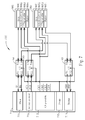
- FIG. 6 is a diagram illustrating a single channel NAND flash memory system 600 of a first embodiment of the present invention.
- the single channel NAND flash memory system 600 of the present invention comprises a NAND flash memory controller 610 , 4 NAND flash memory modules M 1 -M 4 , and 1 remap modules S 1 .
- the NAND flash memory controller 610 comprises a data interface 611 , an action control interface 612 , a chip enable interface 613 , a status interface 614 , and a switch interface 615 .
- the data interface 611 is conjointly coupled to the data interfaces M 11 , M 21 , M 31 , and M 41 for exchanging data with the NAND flash memory modules M 1 -M 4 .
- the data interface 611 has an 8-bit data port, and each data interface of the NAND flash memory modules M 1 -M 4 has an 8-bit data port as well. All the data ports of the NAND flash memory modules are coupled to the same data port of the data interface 611 for exchanging data with 8-bit data width.
- the action control interface 612 is conjointly coupled to the action control interfaces M 12 , M 22 , M 32 , and M 42 for transmitting action control signals to the NAND flash memory modules M 1 -M 4 .
- the action control signals control the actions of the NAND flash memory modules M 1 -M 4 .
- the switch interface 615 is coupled to the control ports Cl of the remap modules S 1 1 for transmitting switch signals to the remap modules S 1 and controlling the internal physical connections of the remap modules S 1 .
- the chip enable interface 613 is respectively coupled to the ports T 1 , T 2 , T 3 , and T 4 of the remap module S 1 through ports CE 1 , CE 2 , CE 3 , and CE 4 for respectively transmitting chip enable signals to the remap module S 1 .
- the remap module SI is respectively coupled to the chip enable interface M 13 , M 23 , M 33 , and M 43 through the ports T 5 , T 6 , T 7 and T 8 .
- Each of T 5 -T 8 ports could be configured to couple to any of T 1 -T 4 ports according to the switch signals received on the control port C 1 of the remap module S 1 .
- the switch interface 615 transmit default switch signals to the remap modules S 1 so that respectively the ports T 1 -T 4 are sequentially coupled to the ports T 5 -T 8 in the remap modules S 1 .
- the NAND flash memory system 600 works the same as the conventional NAND flash memory system 200 . But when one of the NAND flash memory modules is dead, the switch interface 615 transmits switch signals to change the connections between the NAND flash memory controller 610 and the NAND flash memory modules M 1 -M 4 to allow the NAND flash memory system 600 to still work as if no NAND flash memory module is dead but only the total memory size is decreased.
- the switch interface 615 transmits a switch signal to the control port C 1 of the remap modules S 1 for coupling the ports T 1 , T 2 , and T 3 respectively to the ports T 6 , T 7 , T 8 .
- the condition is almost the same as the NAND flash memory system 200 with 3 NAND flash memory modules.
- the difference is the memory size is decreased.
- the chip enable interface 613 is still able to transmit the chip enable signal through the port CE 1 , but the chip enable signal is transmitted, through the remap module S 1 , to the chip enable interface M 23 of the NAND flash memory module M 2 instead of the dead NAND flash memory module M 1 .
- the drawback of the conventional NAND flash memory system is solved and the NAND flash memory system 600 still works with the 3 active NAND flash memory modules.
- the NAND flash memory controller 610 does not have to detect the condition of each NAND flash memory module all the time. Instead, the NAND flash memory controller 610 detects the conditions of the NAND flash memory modules M 1 to M 4 at the beginning, transmits the switch signal to the remap modules S 1 according to the detection result for forming correct connections between the NAND flash memory controller 610 and the NAND flash memory modules M 1 to M 4 , and then the NAND flash memory controller 610 can correctly exchange data with the NAND flash memory modules M 1 to M 4 consequently. Or the controller 610 can detect conditions of the NAND flash memory modules every a period of time to ensure the detection result in compliance with the real condition.
- the amount of the NAND flash memory modules of the NAND flash memory systems 600 are not limited to 4. Instead, the NAND flash memory systems 600 of the present invention can comprises less or more NAND flash memory modules as long as the related design of the remap modules are accordingly changed.
- FIG. 7 is a diagram illustrating a dual channel NAND flash memory system 700 of a second embodiment of the present invention.
- the dual channel NAND flash memory system 700 comprises a NAND flash memory controller 710 , 2 NAND flash memory modules M 6 and M 7 , and 3 swap modules S 3 , S 4 and S 5 .
- the NAND flash memory controller 710 comprises a data interface 711 , an action control interface 712 , a chip enable interface 713 , a status interface 714 , and a swap interface 715 .
- Each NAND flash memory module comprises a data interface, an action control interface, a chip enable interface, and a status interface.
- the NAND flash memory module M 6 comprises a data interface M 61 , an action control interface M 62 , a chip enable interface M 63 , and a status interface M 64 .
- the swap interface 715 is conjointly coupled to the control ports C 1 of the swap modules S 3 , S 4 and S 5 for transmitting switch signals to the swap modules S 3 , S 4 and S 5 and controlling the internal connections of the swap modules S 3 , S 4 and S 5 .
- the chip enable interface 713 is conjointly coupled to the chip enable interface M 63 and M 73 for transmitting chip enable signals to the NAND flash memory modules M 6 and M 7 . For example, if the chip enable interface 713 transmits a chip enable signal, then the NAND flash memory modules M 6 and M 7 are both enabled to execute corresponding actions according to the action control signals.
- the action control interface 712 is respectively coupled to the ports T 1 and T 2 of the swap module S 5 through ports AC 1 and AC 2 for transmitting action control signals to the swap module S 5 .
- the ports T 3 and T 4 of the swap module S 5 are respectively coupled to the action control interfaces M 62 and M 72 .
- Each of the port T 3 and T 4 of the swap module S 5 could be selectively couple to T 1 or T 2 according to the received swap signals on the control port C 1 .
- the action control signals are transmitted through the swap module S 5 to control the actions of the NAND flash memory modules M 6 and M 7 .
- the swap interface 715 transmits a swap signal to the port C 1 of the swap module S 5 for the swap module S 5 coupling the port T 1 and the port T 3 according to the swap signal.
- the action control signal can be transmitted from the port AC 1 of the action control interface 712 , through the ports T 1 and T 3 of the swap module S 5 , to the action control interface M 62 of the NAND flash memory module M 6 , and if the NAND flash memory module M 6 is enabled, the NAND flash memory module M 6 executes corresponding actions according to the action control signals.
- the swap interface 715 transmits a swap signal to the port C 1 of the swap module S 5 for the swap module S 5 coupling the port TI and the port T 4 according to the swap signal.
- the action control signal can be transmitted from the port AC 1 of the action control interface 712 , through the ports T 1 and T 4 of the swap module S 5 , to the action control interface M 72 of the NAND flash memory module M 7 , and if the NAND flash memory module M 7 is enabled, the NAND flash memory module M 7 executes corresponding actions according to the action control signals.
- the data interface 711 is respectively coupled to the ports T 1 and T 2 of the swap module S 4 through the data ports D 1 and D 2 for exchanging data.
- the ports T 3 and T 4 of the swap module S 4 are respectively coupled to the data interfaces M 61 and M 71 .
- Each of the port T 3 and T 4 of the swap module S 4 could be selectively couple to T 1 or T 2 according to the received swap signals on the control port Cl.
- the data are exchanged through the swap module S 4 with the data interface M 61 and M 71 of the NAND flash memory modules M 6 and M 7 .
- the data ports D 1 and D 2 are both an 8-bit data port, and each data interface of the NAND flash memory modules M 6 and M 7 has an 8-bit data port as well. Therefore the ports T 1 , T 2 , T 3 , and T 4 of the swap module S 4 are 8-bit data ports.
- the status interface 714 is respectively coupled to the ports T 1 and T 2 of the swap module S 3 through the data ports RB 1 and RB 2 for exchanging data.
- the ports T 3 and T 4 of the swap module S 3 are respectively coupled to the status interfaces M 64 and M 74 .
- Each of the port T 3 and T 4 of the swap module S 3 could be selectively couple to T 1 or T 2 according to the received swap signals on the control port C 1 .
- the status signals are transmitted through the swap module S 3 to indicate the status of the NAND flash memory modules M 6 and M 7 .
- the swap interface 715 does transmit default swap signals to the swap modules S 3 , S 4 and S 5 so that respectively the ports T 1 and T 2 are sequentially coupled to the ports T 3 and T 4 in the swap modules S 3 , S 4 and S 5 .
- the NAND flash memory system 700 works the same as the conventional NAND flash memory system 300 .
- the switch interface 715 transmits swap signals to change the connections between the NAND flash memory controller 710 and the NAND flash memory modules M 6 and M 7 to allow the NAND flash memory system 700 to still work as a single channel system with total memory size decreased for 50%.
- the swap interface 715 transmits a swap signal to the control port C 1 of the remap modules S 3 , S 4 and S 5 for coupling the ports T 1 to the port T 4 and T 2 to the port T 3 in the swap modules S 3 , S 4 and S 5 .
- the condition is almost the same as the NAND flash memory system 100 .
- the action control interface 712 is still able to transmit the action control signal through the port AC 1 , but the action control signal is transmitted, through the swap module S 5 , to the action control interface M 72 of the NAND flash memory module M 7 instead of the dead NAND flash memory module M 6 .
- the swap interface 715 transmits default swap signal and the NAND flash memory system 700 still works as a single channel NAND flash memory system with the active NAND flash memory module M 6 .
- the drawback of the conventional NAND flash memory system is solved and the NAND flash memory system 700 still works with the 1 active NAND flash memory module.
- the NAND flash memory controller 710 does not have to detect the condition of each NAND flash memory module all the time. Instead, the NAND flash memory controller 710 detects the conditions of the NAND flash memory modules M 6 and M 7 at the beginning, transmits the swap signal to the swap modules S 3 , S 4 and S 5 according to the detection result for forming correct connections between the NAND flash memory controller 710 and the NAND flash memory modules M 6 and M 7 , and then the NAND flash memory controller 710 can correctly exchange data with the NAND flash memory modules M 6 and M 7 consequently. Or the controller 510 can detect conditions of the NAND flash memory modules every a period of time to ensure the detection result in compliance with the real condition.
- FIG. 8 is a diagram illustrating a dual channel NAND flash memory system 800 of a third embodiment of the present invention. All the components in FIG. 8 are similar to those in FIG. 7 and thus the related description is omitted.
- the difference between the dual channel NAND flash memory system 700 and the dual channel NAND flash memory system 800 is that the dual channel NAND flash memory system 800 does not comprises the swap module S 3 and S 4 . Instead, the status interface of each NAND flash memory module in FIG. 8 is conjointly coupled to the status interface 814 of the NAND flash memory controller 810 . In this way, as long as M 8 or M 9 is busy, the NAND flash memory controller 810 considers both the NAND flash memory modules M 8 and M 9 are busy and halts the related action. The related action is not continued until all the NAND flash memory modules M 8 and M 9 are ready.
- the design in FIG. 8 of the present invention can save two swap modules.
- FIG. 9 is a diagram illustrating a dual channel NAND flash memory system 900 of a fourth embodiment of the present invention.
- the dual channel NAND flash memory system 900 comprises a NAND flash memory controller 910 , 4 NAND flash memory modules M 11 , M 12 , M 13 and M 14 , and 1 remap modules S 6 and 3 swap modules S 7 , S 8 and S 9 .
- the NAND flash memory controller 910 comprises a data interface 911 , an action control interface 912 , a chip enable interface 913 , a status interface 914 , a switch interface 915 , and a swap interface 916 .
- the NAND flash memory modules M 11 -M 1 4 are the same as the NAND flash memory module M 1 .
- the data interface 911 has two ports D 1 and D 2 respectively coupled to the ports T 1 and T 2 of the swap module S 7 . Both of the ports D 1 and D 2 transmit or receive data with 8-bit width so that the total data width is doubled.
- the swap module S 7 has 4 ports T 1 to T 4 , and a control port C 1 .
- the ports T 3 of the swap module S 7 is coupled to the data interface M 111 of the NAND flash module M 11 and the data interface M 121 of the NAND flash module M 12 .
- the ports T 4 of the swap module S 7 is coupled to the data interface M 131 of the NAND flash module M 13 and the data interface M 141 of the NAND flash module M 14 .
- Each of the port T 3 and T 4 of the swap module S 7 could be selectively couple to T 1 or T 2 according to the received swap signals on the control port C 1 .
- the port D 1 of the data interface 911 is conjointly coupled to the data interfaces M 111 and M 121 .
- the data ports D 1 and D 2 of the data interface 911 are both an 8-bit data port, and each data interface of the NAND flash memory modules M 11 to M 14 has an 8-bit data port as well. Therefore the ports T 1 , T 2 , T 3 , and T 4 of the swap module S 7 are 8-bit data ports.
- the action control interface 912 has two ports AC 1 and AC 2 respectively coupled to the ports T 1 and T 2 of the swap module S 8 . Both of the ports AC 1 and AC 2 transmit action control signals for controlling actions of the NAND flash modules.
- the swap module S 8 has 4 ports T 1 to T 4 , and a control port C 1 .
- the ports T 3 of the swap module S 8 is coupled to the action control interface M 112 of the NAND flash module M 11 and the action control interface M 122 of the NAND flash module M 12 .
- the ports T 4 of the swap module S 8 is coupled to the action control interface M 132 of the NAND flash module M 13 and the action control interface M 142 of the NAND flash module M 14 .
- Each of the port T 3 and T 4 of the swap module S 8 could be selectively couple to T 1 or T 2 according to the received swap signals on the control port C 1 . For example, if the port T 1 of the swap module S 8 is coupled to the port T 3 , the port AC 1 of the action control interface 912 is conjointly coupled to the action control interfaces M 112 and M 122 .
- the chip enable interface 913 has four ports CE 1 -CE 4 .
- CE 1 and CE 2 are respectively coupled to the ports T 1 and T 2 of the remap module S 6 . Both of the ports CE 1 and CE 2 transmit chip enable signals for enabling the NAND flash modules.
- the remap module S 6 has 8 ports T 1 to T 8 , and a control port C 1 .
- the ports T 5 of the remap module S 6 is coupled to the chip enable interface M 113 of the NAND flash module M 11 and the chip enable interface M 133 of the NAND flash module M 13 .
- the ports T 6 of the remap module S 6 is coupled to the chip enable interface M 123 of the NAND flash module M 12 and the chip enable interface M 143 of the NAND flash module M 14 .
- the T 5 ⁇ T 8 port of the remap module S 6 could couple to any of T 1 to T 4 ports. For example, if the port T 5 of the remap module S 6 is coupled to the port T 1 , the port CE 1 of the chip enable interface 913 is conjointly coupled to the chip enable control interfaces M 113 and M 133 .
- the status interface 914 has two ports RB 1 and RB 2 respectively coupled to the ports T 1 and T 2 of the swap module S 9 . Both of the ports RB 1 and RB 2 receive status signals for informing if the NAND flash modules are ready to the NAND flash memory controller 910 .
- the swap module S 9 has 4 ports T 1 to T 4 , and a control port C 1 .
- the ports T 3 of the swap module S 9 is coupled to the status interface M 114 of the NAND flash module M 11 and the status interface M 124 of the NAND flash module M 12 .
- the ports T 4 of the swap module S 9 is coupled to the status interface M 134 of the NAND flash module M 13 and the status interface M 144 of the NAND flash module M 14 .
- Each of the port T 3 and T 4 of the swap module S 9 could be selectively couple to T 1 or T 2 according to the received swap signals on the control port C 1 . For example, if the port T 3 of the swap module S 9 is coupled to the port T 1 , the port RB 1 of the status interface 914 is conjointly coupled to the status control interfaces M 114 and M 124 .
- the swap interface 916 is conjointly coupled to the control ports C 1 of the swap modules S 7 , S 8 and S 9 for transmitting swap signals to the swap modules S 7 , S 8 and S 9 and controlling the internal connections of the swap modules S 7 , S 8 and S 9 .
- the switch interface 915 is coupled to the control ports C 1 of the remap modules S 6 for transmitting switch signals to the remap modules S 6 and controlling the internal connections of the remap modules S 6 .
- the data interface 911 can transmit data to the data interface M 111 of the NAND flash memory module M 11 and the data interface M 121 of the NAND flash memory module M 12 through the port D 1 , and can transmit data to the data interface M 131 of the NAND flash memory module M 13 and the data interface M 141 of the NAND flash memory module M 14 through the port D 2 .
- the action control interface 912 can transmit action control signals to the action control interface M 112 of the NAND flash memory module M 11 and the action control interface M 122 of the NAND flash memory module M 12 through the port AC 1 , and can transmit action control signals to the action control interface M 132 of the NAND flash memory module M 13 and the action control interface M 142 of the NAND flash memory module M 14 through the port AC 2 .
- the chip enable interface 913 can transmit chip enable signals to the chip enable interface M 113 of the NAND flash memory module M 11 and the chip enable interface M 133 of the NAND flash memory module M 13 through the port CE 1 , and can transmit chip enable signals to the chip enable interface M 123 of the NAND flash memory module M 12 and the chip enable interface M 143 of the NAND flash memory module M 14 through the port CE 2 .
- the status interface 914 can receive status signals from the status interface M 114 of the NAND flash memory module M 11 and the status interface M 124 of the NAND flash memory module M 12 through the port RB 1 , and can receive status signals from the status interface M 134 of the NAND flash memory module M 13 and the status interface M 144 of the NAND flash memory module M 14 through the port RB 2 .
- the NAND flash memory controller 910 When the NAND flash memory controller 910 detects one of the NAND flash memory modules M 11 to M 14 , the NAND flash memory controller could transmit swap signals and switch signals to configure the NAND flash memory controller for avoiding the NAND flash memory system failing.
- the NAND flash memory controller could transmit swap signals to change the internal connections of the swap modules S 7 , S 8 and S 9 , the ports T 3 of the swap modules S 7 , S 8 and S 9 are respectively coupled to the ports T 2 of the swap modules S 7 , S 8 and S 9 , and the ports T 1 of the swap modules S 7 , S 8 and S 9 are respectively coupled to the ports T 4 of the swap modules S 7 , S 8 and S 9 .
- the NAND flash memory system 900 still works as a single channel memory system 200 with the NAND flash memory modules M 13 and M 14 .
- the choice 2 is the NAND flash memory controller could transmit switch signal to change the internal connections of the remap modules S 6 , the port T 1 of the remap modules S 6 is coupled to the ports T 6 of the remap modules S 6 .
- the NAND flash memory system 900 still works as a dual channel memory system 300 with the NAND flash memory modules M 12 and M 14 .
- the amount of the NAND flash memory modules of the NAND flash memory systems 600 , 700 , 800 , 900 are not limited. Instead, the NAND flash memory systems 600 , 700 , 800 , 900 of the present invention can comprise less or more NAND flash memory modules.
- NAND flash memory controller has two data ports and four chip enable ports. If the number of data ports or chip enable ports of the NAND flash memory controller are different from the NAND flash memory controller shown in above embodiments, the swap module and remap module are according changed. For example, if the NAND flash memory controller has two chip enable ports only, then the remap module could be designed to have four ports T 1 ⁇ T 4 and a control port C 1 . The T 3 and T 4 could be configured to couple to T 1 or T 2 port.
- the amount of the swap modules does not have to be as the same as the figures shows.
- the status interfaces M 64 and M 74 can be both coupled to the port RB 1 of the flash memory controller 710 .
- the swap module S 3 can be saved.
- the high-byte flash memory module (for example, M 6 ) and low-byte flash memory module (for example, M 7 ) are coupled to different port of the flash memory controller, then a swap module is required.
- the flash memory modules M 6 and M 7 connects to different data/action/status ports. Therefore, 3 swap modules are required.
- FIG. 10 is a diagram illustrating a swap module 1000 disposed in a 4-channel NAND flash memory system.
- the 4 ports T 1 , T 2 , T 3 , and T 4 of the swap module 1000 are respectively coupled to the data ports D 1 , D 2 , D 3 , and D 4 of a NAND flash memory controller.
- the 4 ports T 5 , T 6 , T 7 , and T 8 of the swap module 1000 are respectively coupled to the data ports of the NAND flash memory modules A, B, C, and D.
- Each of T 5 -T 8 port could be configured to couple to any of T 1 -T 4 port according to the swap signals received on the control port C 1 .
- the control port C 1 of the swap module 1000 is coupled to the swap interface of the NAND flash memory controller.
- the NAND flash memory controller adjusts the connections between the NAND flash memory controller and the NAND flash memory modules A, B, C, D by controlling the swap module 1000 according to the status (live or dead) of the NAND flash memory modules A, B, C, and D.
- FIG. 11 is a diagram illustrating the default status of the swap module 1000 .
- the ports T 1 , T 2 , T 3 , and T 4 are respectively coupled to the ports T 5 , T 6 , T 7 , and T 8 .
- the data ports D 1 , D 2 , D 3 , and D 4 of the NAND flash memory controller are respectively coupled to the data ports of the NAND flash memory modules A, B, C, and D.
- FIG. 12 is a diagram illustrating the internal connections of the swap module 1000 when the NAND flash memory module A is dead.
- the NAND flash memory controller finds the NAND flash memory module A dead, the NAND flash the port T 6 coupled to the port T 1 , the port T 7 coupled to the port T 2 , the port T 8 coupled to the port T 3 .
- the NAND flash memory system still works as a 3-channel NAND flash memory system.
- FIG. 13 is a diagram illustrating the internal connections of the swap module 1000 when the NAND flash memory modules B and C are dead. As shown in FIG. 13 , after the NAND flash memory controller finds the NAND flash memory modules B and C dead, the NAND flash memory controller controls the ports T 5 coupled to the port T 1 , and the port T 8 coupled to the port T 2 . In this way, the NAND flash memory system still works as a 2-channel NAND flash memory system.
- the swap module has to be disposed when the flash memory modules are coupled to different ports of the flash memory controller. Therefore, if the flash memory modules are coupled to the same port of the flash memory controller, then the swap module can be saved.
- the NAND flash memory controller, the swap modules, and the remap modules, can be merged in a chip.
- FIG. 14 is a diagram illustrating a NAND flash memory system 1400 of a fifth embodiment of the present invention.
- the NAND flash memory system 1400 comprises a NAND flash memory controller 1410 , a universal connection device 1420 , and a plurality of NAND flash memory modules M 1 ⁇ MQ.
- the spirit of the NAND flash memory system 1400 is to provide a system using a same Print Circuit Board (PCB) with different applications.
- PCB Print Circuit Board
- the amounts of ports of data interface, the action control interface, the chip enable interface, and the status interface of the NAND flash memory controller 1410 is designed according to the user's need.
- the amounts of NAND flash memory modules also can be designed according to the user's need.
- All ports from the NAND flash memory controller 1410 are coupled to the universal connection device 1420 , and all ports from the NAND flash memory modules are coupled to the universal connection device 1420 .
- the switch interface 14152 and swap interface 14151 of the NAND flash memory controller controls the internal connections of the universal connection device 1420 .
- the connections between the NAND flash memory controller 1410 and the plurality of the NAND flash memory modules can be changed by controlling the internal connections of the universal connection device 1420 .
- each of the flash memory system requires different PCB.
- the user can utilize a universal PCB for the single, dual, single-channel interleaved, dual-channel interleaved or multiple channel NAND flash memory systems as long as the universal connection device 1420 is included. Thus, efforts to maintain these PCBs can be saved.
- FIG. 15 is a diagram illustrating the details of the universal connection device 1420 which could support single and dual-channel systems and 4 ports CE 1 to CE 4 at most.
- the universal connection device 1420 comprises 3 swap modules SA, SB, and SD and 1 switch module SC.
- Each of the swap modules SA, SB, and SD has ports T 1 ⁇ T 4 .
- the switch module SC has ports T 1 ⁇ T 8 .
- the internal connections of all the modules SA ⁇ SD can be controlled through their control ports C 1 . Therefore, the controller 1410 can control a single-channel system or a dual-channel system through programming the internal connections of the modules SA ⁇ SD of the universal connection device 1420 .
- FIG. 16 shows a NAND flash memory system which comprises one dual-channel NAND flash memory controller and 2 NAND flash memory modules. If the NAND flash memory system is to be configured as a dual-channel NAND flash memory system. Then the NAND flash memory controller transmits swap signal to make T 1 and T 2 couple to T 3 and T 4 in the three swap modules. The NAND flash memory controller also transmits a switch signal to make T 5 couple to T 1 and T 6 couple to T 1 in the switch module. Then the NAND flash system is like NAND flash memory system 300 which is a dual-channel NAND flash memory system.
- FIG. 17 and FIG. 18 show a NAND flash memory system which comprises the same components as shown in FIG. 16 . If the NAND flash memory system is to be configured as a single-channel NAND flash memory system, Then the NAND flash memory controller transmits swap signal to make T 1 and T 2 couple to T 3 and T 4 in the three swap modules when CE 1 is 0 and CE 2 is 1. The NAND flash memory controller also transmits a swap signal to make T 1 and T 2 couple to T 4 and T 3 in the three swap modules when CE 1 is 1 CE 2 is 0. Then the NAND flash memory system is like NAND flash memory system 200 with 2 NAND flash memory.
- FIG. 19 illustrates the NAND flash memory controller have single-channel interface, the same PCB could also be used. If the NAND flash memory controller is single-channel, then the swap interface transmits a swap signal to make T 1 couple to T 3 and T 1 couple to T 4 in the three swap modules. Then, the NAND flash memory system is like NAND flash memory system 200 with 2 NAND flash modules.
- the NAND flash memory system of the present invention can be NAND flash memory card system, USB NAND flash disk system, SATA NAND flash disk system, solid-state-disk NAND flash disk system, PCI express NAND flash disk system.
- the present invention provides a flexible NAND flash memory system capable of changing the connections between the NAND flash memory controller and the NAND flash memory modules. In this way, when a NAND flash memory module is dead, the system still works with the active NAND flash memory modules. And the PCB requirement can be reduced by the present invention.
Abstract
Description
Claims (61)
Priority Applications (1)
| Application Number | Priority Date | Filing Date | Title |
|---|---|---|---|
| US11/753,572 US7752383B2 (en) | 2007-05-25 | 2007-05-25 | NAND flash memory system with programmable connections between a NAND flash memory controller and a plurality of NAND flash memory modules and method thereof |
Applications Claiming Priority (1)
| Application Number | Priority Date | Filing Date | Title |
|---|---|---|---|
| US11/753,572 US7752383B2 (en) | 2007-05-25 | 2007-05-25 | NAND flash memory system with programmable connections between a NAND flash memory controller and a plurality of NAND flash memory modules and method thereof |
Publications (2)
| Publication Number | Publication Date |
|---|---|
| US20080294836A1 US20080294836A1 (en) | 2008-11-27 |
| US7752383B2 true US7752383B2 (en) | 2010-07-06 |
Family
ID=40073465
Family Applications (1)
| Application Number | Title | Priority Date | Filing Date |
|---|---|---|---|
| US11/753,572 Active 2028-09-05 US7752383B2 (en) | 2007-05-25 | 2007-05-25 | NAND flash memory system with programmable connections between a NAND flash memory controller and a plurality of NAND flash memory modules and method thereof |
Country Status (1)
| Country | Link |
|---|---|
| US (1) | US7752383B2 (en) |
Cited By (3)
| Publication number | Priority date | Publication date | Assignee | Title |
|---|---|---|---|---|
| US20120077357A1 (en) * | 2010-09-25 | 2012-03-29 | Bin Zou | Self referencing pin |
| TWI715992B (en) * | 2018-12-20 | 2021-01-11 | 南亞科技股份有限公司 | Memory device, memory system and method of reading from memory device |
| US11783874B2 (en) | 2020-09-29 | 2023-10-10 | Samsung Electronics Co., Ltd. | Memory with swap mode |
Families Citing this family (1)
| Publication number | Priority date | Publication date | Assignee | Title |
|---|---|---|---|---|
| US10891057B1 (en) * | 2015-12-31 | 2021-01-12 | EMC IP Holding Company LLC | Optimizing flash device write operations |
Citations (4)
| Publication number | Priority date | Publication date | Assignee | Title |
|---|---|---|---|---|
| US5530673A (en) * | 1993-04-08 | 1996-06-25 | Hitachi, Ltd. | Flash memory control method and information processing system therewith |
| US5608673A (en) * | 1994-07-25 | 1997-03-04 | Samsung Electronics Co., Ltd. | Nand-type flash memory integrated-circuit card |
| US6684290B2 (en) * | 2001-10-18 | 2004-01-27 | Kabushiki Kaisha Toshiba | Memory rewriting apparatus and method for memory mapping rewriting program to same address space |
| US20050268208A1 (en) * | 2004-05-31 | 2005-12-01 | Sony Corporation | Semiconductor memory device and signal processing system |
-
2007
- 2007-05-25 US US11/753,572 patent/US7752383B2/en active Active
Patent Citations (4)
| Publication number | Priority date | Publication date | Assignee | Title |
|---|---|---|---|---|
| US5530673A (en) * | 1993-04-08 | 1996-06-25 | Hitachi, Ltd. | Flash memory control method and information processing system therewith |
| US5608673A (en) * | 1994-07-25 | 1997-03-04 | Samsung Electronics Co., Ltd. | Nand-type flash memory integrated-circuit card |
| US6684290B2 (en) * | 2001-10-18 | 2004-01-27 | Kabushiki Kaisha Toshiba | Memory rewriting apparatus and method for memory mapping rewriting program to same address space |
| US20050268208A1 (en) * | 2004-05-31 | 2005-12-01 | Sony Corporation | Semiconductor memory device and signal processing system |
Cited By (5)
| Publication number | Priority date | Publication date | Assignee | Title |
|---|---|---|---|---|
| US20120077357A1 (en) * | 2010-09-25 | 2012-03-29 | Bin Zou | Self referencing pin |
| US8465297B2 (en) * | 2010-09-25 | 2013-06-18 | Intel Corporation | Self referencing pin |
| TWI512859B (en) * | 2010-09-25 | 2015-12-11 | Intel Corp | Socket and package apparatus to reduce induced crosstalk, computing system and method of constructing a socket pin |
| TWI715992B (en) * | 2018-12-20 | 2021-01-11 | 南亞科技股份有限公司 | Memory device, memory system and method of reading from memory device |
| US11783874B2 (en) | 2020-09-29 | 2023-10-10 | Samsung Electronics Co., Ltd. | Memory with swap mode |
Also Published As
| Publication number | Publication date |
|---|---|
| US20080294836A1 (en) | 2008-11-27 |
Similar Documents
| Publication | Publication Date | Title |
|---|---|---|
| US11380667B2 (en) | Memory device with a multiplexed command/address bus | |
| US7987308B2 (en) | Multi-interface controller, memory card having the multi-interface controller, and interface setting method | |
| KR100833176B1 (en) | Efficient connection between modules of removable electronic circuit cards | |
| US9025409B2 (en) | Memory buffers and modules supporting dynamic point-to-point connections | |
| US7802043B2 (en) | Methods and apparatus for adding an autonomous controller to an existing architecture | |
| US7752383B2 (en) | NAND flash memory system with programmable connections between a NAND flash memory controller and a plurality of NAND flash memory modules and method thereof | |
| US10325637B2 (en) | Flexible point-to-point memory topology | |
| US20100023669A1 (en) | Host controller disposed in multi-function card reader | |
| CN112951315A (en) | NVME \ AHCI compatible dual-protocol hard disk testing device and method | |
| CN102201260B (en) | Apparatus and method for communicating parameter of inverter | |
| CN114253898A (en) | Bus device and data read-write circuit | |
| US9158609B2 (en) | Universal serial bus testing device | |
| CN108255760A (en) | A kind of multipath I 2 C system and data read-write method | |
| TWI613586B (en) | Single input/output cell with multiple bond pads and/or transmitters | |
| US9116797B2 (en) | Flash memory devices including reserve units operating in abnormal situations and controlling methods thereof | |
| US11216401B2 (en) | USB host-to-USB host chip | |
| CN107643989B (en) | Dual-optical-fiber loop redundancy structure communication board card based on PCI bus protocol | |
| US20080250177A1 (en) | Memory device including connector for independently interfacing host and memory devices | |
| KR100891951B1 (en) | Common module for ddr? sdram and ddr? sdram | |
| US20150348651A1 (en) | Multiple access test architecture for memory storage devices | |
| JP5640941B2 (en) | Process data monitoring system | |
| US20210271625A1 (en) | NVMe-MI Over SMBus Multi-Master Controller with other SMBus and I2C Masters in a Single FPGA Chip | |
| US20080151591A1 (en) | Memory system with a configurable number of read data bits | |
| JP2021144559A (en) | Memory system and information processing system | |
| KR101192594B1 (en) | Direct data transfer between slave devices |
Legal Events
| Date | Code | Title | Description |
|---|---|---|---|
| AS | Assignment |
Owner name: SKYMEDI CORPORATION, TAIWAN Free format text: ASSIGNMENT OF ASSIGNORS INTEREST;ASSIGNORS:CHENG, CHUANG;CHEN, CHING-CHANG;SUGAWA, SATOSHI;AND OTHERS;REEL/FRAME:019342/0356;SIGNING DATES FROM 20070316 TO 20070321 Owner name: SKYMEDI CORPORATION, TAIWAN Free format text: ASSIGNMENT OF ASSIGNORS INTEREST;ASSIGNORS:CHENG, CHUANG;CHEN, CHING-CHANG;SUGAWA, SATOSHI;AND OTHERS;SIGNING DATES FROM 20070316 TO 20070321;REEL/FRAME:019342/0356 |
|
| AS | Assignment |
Owner name: SKYMEDI CORPORATION, TAIWAN Free format text: ASSIGNMENT OF ASSIGNORS INTEREST;ASSIGNOR:CHANG, WEN-LIN;REEL/FRAME:021477/0339 Effective date: 20080704 |
|
| STCF | Information on status: patent grant |
Free format text: PATENTED CASE |
|
| FPAY | Fee payment |
Year of fee payment: 4 |
|
| MAFP | Maintenance fee payment |
Free format text: PAYMENT OF MAINTENANCE FEE, 8TH YR, SMALL ENTITY (ORIGINAL EVENT CODE: M2552) Year of fee payment: 8 |
|
| MAFP | Maintenance fee payment |
Free format text: PAYMENT OF MAINTENANCE FEE, 12TH YR, SMALL ENTITY (ORIGINAL EVENT CODE: M2553); ENTITY STATUS OF PATENT OWNER: SMALL ENTITY Year of fee payment: 12 |