US7759407B2 - Composition for adhering materials together - Google Patents
Composition for adhering materials together Download PDFInfo
- Publication number
- US7759407B2 US7759407B2 US11/187,406 US18740605A US7759407B2 US 7759407 B2 US7759407 B2 US 7759407B2 US 18740605 A US18740605 A US 18740605A US 7759407 B2 US7759407 B2 US 7759407B2
- Authority
- US
- United States
- Prior art keywords
- composition
- functional group
- functional
- polymerizable material
- cross
- Prior art date
- Legal status (The legal status is an assumption and is not a legal conclusion. Google has not performed a legal analysis and makes no representation as to the accuracy of the status listed.)
- Active, expires
Links
- 0 C.C.C.C.C.C.C*(C)CC(C)C.C*C Chemical compound C.C.C.C.C.C.C*(C)CC(C)C.C*C 0.000 description 3
- NQYKXDNBXBYKFC-UHFFFAOYSA-N C.C.C.C.C=CC(=O)OCC(O)COc1c(C)cccc1Cc1cccc(CC)c1OCC(O)COC(=O)C1CC=CCC1C(=O)O.CC.CC Chemical compound C.C.C.C.C=CC(=O)OCC(O)COc1c(C)cccc1Cc1cccc(CC)c1OCC(O)COC(=O)C1CC=CCC1C(=O)O.CC.CC NQYKXDNBXBYKFC-UHFFFAOYSA-N 0.000 description 3
- PSGCQDPCAWOCSH-UHFFFAOYSA-N C=CC(=O)OC1CC2CCC1(C)C2(C)C Chemical compound C=CC(=O)OC1CC2CCC1(C)C2(C)C PSGCQDPCAWOCSH-UHFFFAOYSA-N 0.000 description 1
- CYUZOYPRAQASLN-UHFFFAOYSA-N C=CC(=O)OCCC(=O)O Chemical compound C=CC(=O)OCCC(=O)O CYUZOYPRAQASLN-UHFFFAOYSA-N 0.000 description 1
- LNMQRPPRQDGUDR-UHFFFAOYSA-N C=CC(=O)OCCCCCC Chemical compound C=CC(=O)OCCCCCC LNMQRPPRQDGUDR-UHFFFAOYSA-N 0.000 description 1
- KUDUQBURMYMBIJ-UHFFFAOYSA-N C=CC(=O)OCCOC(=O)C=C Chemical compound C=CC(=O)OCCOC(=O)C=C KUDUQBURMYMBIJ-UHFFFAOYSA-N 0.000 description 1
- PKFOWTHVQGBTEM-UHFFFAOYSA-N C=CC(=O)Oc1ccc(C(C)(C)c2ccc(OCC3CO3)cc2)cc1 Chemical compound C=CC(=O)Oc1ccc(C(C)(C)c2ccc(OCC3CO3)cc2)cc1 PKFOWTHVQGBTEM-UHFFFAOYSA-N 0.000 description 1
- XMLYCEVDHLAQEL-UHFFFAOYSA-N CC(C)(O)C(=O)C1=CC=CC=C1 Chemical compound CC(C)(O)C(=O)C1=CC=CC=C1 XMLYCEVDHLAQEL-UHFFFAOYSA-N 0.000 description 1
- GJKGAPPUXSSCFI-UHFFFAOYSA-N CC(C)(O)C(=O)c1ccc(OCCO)cc1 Chemical compound CC(C)(O)C(=O)c1ccc(OCCO)cc1 GJKGAPPUXSSCFI-UHFFFAOYSA-N 0.000 description 1
Images


Classifications
-
- G—PHYSICS
- G03—PHOTOGRAPHY; CINEMATOGRAPHY; ANALOGOUS TECHNIQUES USING WAVES OTHER THAN OPTICAL WAVES; ELECTROGRAPHY; HOLOGRAPHY
- G03F—PHOTOMECHANICAL PRODUCTION OF TEXTURED OR PATTERNED SURFACES, e.g. FOR PRINTING, FOR PROCESSING OF SEMICONDUCTOR DEVICES; MATERIALS THEREFOR; ORIGINALS THEREFOR; APPARATUS SPECIALLY ADAPTED THEREFOR
- G03F7/00—Photomechanical, e.g. photolithographic, production of textured or patterned surfaces, e.g. printing surfaces; Materials therefor, e.g. comprising photoresists; Apparatus specially adapted therefor
- G03F7/0002—Lithographic processes using patterning methods other than those involving the exposure to radiation, e.g. by stamping
-
- B—PERFORMING OPERATIONS; TRANSPORTING
- B82—NANOTECHNOLOGY
- B82Y—SPECIFIC USES OR APPLICATIONS OF NANOSTRUCTURES; MEASUREMENT OR ANALYSIS OF NANOSTRUCTURES; MANUFACTURE OR TREATMENT OF NANOSTRUCTURES
- B82Y10/00—Nanotechnology for information processing, storage or transmission, e.g. quantum computing or single electron logic
-
- B—PERFORMING OPERATIONS; TRANSPORTING
- B82—NANOTECHNOLOGY
- B82Y—SPECIFIC USES OR APPLICATIONS OF NANOSTRUCTURES; MEASUREMENT OR ANALYSIS OF NANOSTRUCTURES; MANUFACTURE OR TREATMENT OF NANOSTRUCTURES
- B82Y40/00—Manufacture or treatment of nanostructures
-
- G—PHYSICS
- G03—PHOTOGRAPHY; CINEMATOGRAPHY; ANALOGOUS TECHNIQUES USING WAVES OTHER THAN OPTICAL WAVES; ELECTROGRAPHY; HOLOGRAPHY
- G03F—PHOTOMECHANICAL PRODUCTION OF TEXTURED OR PATTERNED SURFACES, e.g. FOR PRINTING, FOR PROCESSING OF SEMICONDUCTOR DEVICES; MATERIALS THEREFOR; ORIGINALS THEREFOR; APPARATUS SPECIALLY ADAPTED THEREFOR
- G03F7/00—Photomechanical, e.g. photolithographic, production of textured or patterned surfaces, e.g. printing surfaces; Materials therefor, e.g. comprising photoresists; Apparatus specially adapted therefor
- G03F7/004—Photosensitive materials
- G03F7/038—Macromolecular compounds which are rendered insoluble or differentially wettable
- G03F7/0388—Macromolecular compounds which are rendered insoluble or differentially wettable with ethylenic or acetylenic bands in the side chains of the photopolymer
Abstract
Description

and comprises approximately 47% of bulk material by weight, but may be present in a range of 20% to 80%, inclusive. As a result, the mechanical properties of
and comprises approximately 25% of bulk material by weight, but may be present in a range of 0% to 50%, inclusive. Also providing flexibility to

and comprises approximately 25% of bulk material by weight, and may be present in a range of 10% to 50%, inclusive. EGDA also contributes to the modulus and stiffness buildup, as well as facilitates cross-linking of n-HA and IBOA during polymerization of the bulk material.

and comprises approximately 3% of the bulk material by weight, and may be present in a range of 1% to 5%, inclusive. The actinic energy to which the initiator is responsive is broadband ultraviolet energy generated by a medium-pressure mercury lamp. In this manner, the initiator facilitates cross-linking and polymerization of the components of the bulk material.

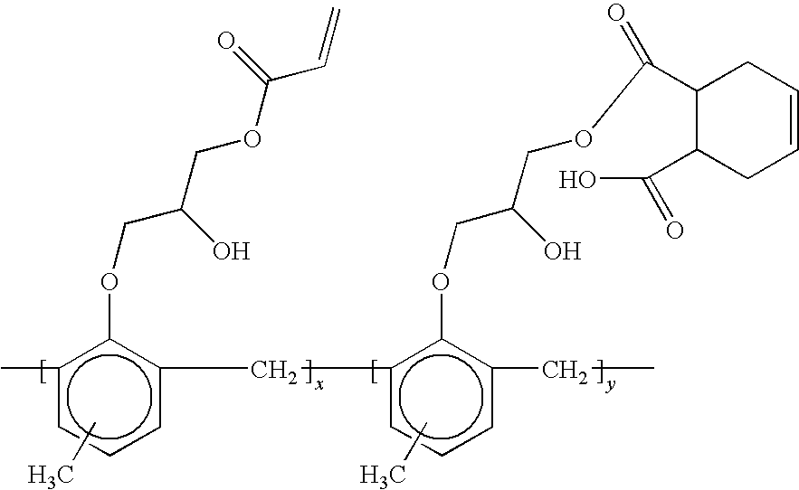
In which R, R′, R″ and R′″ are linking groups and x, y, z are averaged repeating numbers of the groups associated therewith. These repeating units could be randomly distributed. The groups X and X′ denote the functional groups, with the understanding that typically, the functional group X differs from functional group X′. One of the functional groups X and X′, for example X′, is selected to achieve cross-reaction with the material from which
The X′

The X′

where x and y are integers indicating repeating units that are randomly distributed. The X′
The X′
Claims (21)

Priority Applications (12)
| Application Number | Priority Date | Filing Date | Title |
|---|---|---|---|
| US11/187,407 US8557351B2 (en) | 2005-07-22 | 2005-07-22 | Method for adhering materials together |
| US11/187,406 US7759407B2 (en) | 2005-07-22 | 2005-07-22 | Composition for adhering materials together |
| SG201005033-4A SG163605A1 (en) | 2005-07-22 | 2006-06-05 | Method and composition for adhering materials together |
| CN2006800266865A CN101228013B (en) | 2005-07-22 | 2006-06-05 | Method and composition for adhering materials together |
| JP2008522785A JP5084728B2 (en) | 2005-07-22 | 2006-06-05 | Method and composition for bonding materials together |
| PCT/US2006/021948 WO2007050133A2 (en) | 2005-07-22 | 2006-06-05 | Method and composition for adhering materials together |
| KR1020087003583A KR101416112B1 (en) | 2005-07-22 | 2006-06-05 | Method and composition for adhering materials together |
| EP06844135.1A EP1915888B1 (en) | 2005-07-22 | 2006-06-05 | Method and composition for adhering materials together |
| TW095121031A TWI329239B (en) | 2005-07-22 | 2006-06-13 | Method and composition for adhering materials together |
| US11/734,542 US8808808B2 (en) | 2005-07-22 | 2007-04-12 | Method for imprint lithography utilizing an adhesion primer layer |
| US12/326,709 US8846195B2 (en) | 2005-07-22 | 2008-12-02 | Ultra-thin polymeric adhesion layer |
| US14/048,745 US20140034229A1 (en) | 2005-07-22 | 2013-10-08 | Method for Adhering Materials Together |
Applications Claiming Priority (2)
| Application Number | Priority Date | Filing Date | Title |
|---|---|---|---|
| US11/187,407 US8557351B2 (en) | 2005-07-22 | 2005-07-22 | Method for adhering materials together |
| US11/187,406 US7759407B2 (en) | 2005-07-22 | 2005-07-22 | Composition for adhering materials together |
Related Parent Applications (2)
| Application Number | Title | Priority Date | Filing Date |
|---|---|---|---|
| US11/187,407 Continuation-In-Part US8557351B2 (en) | 2005-07-22 | 2005-07-22 | Method for adhering materials together |
| US11/187,407 Division US8557351B2 (en) | 2005-07-22 | 2005-07-22 | Method for adhering materials together |
Related Child Applications (4)
| Application Number | Title | Priority Date | Filing Date |
|---|---|---|---|
| US11/187,407 Continuation-In-Part US8557351B2 (en) | 2005-07-22 | 2005-07-22 | Method for adhering materials together |
| US11/187,407 Division US8557351B2 (en) | 2005-07-22 | 2005-07-22 | Method for adhering materials together |
| US11/734,542 Continuation-In-Part US8808808B2 (en) | 2005-07-22 | 2007-04-12 | Method for imprint lithography utilizing an adhesion primer layer |
| US12/326,709 Continuation-In-Part US8846195B2 (en) | 2005-07-22 | 2008-12-02 | Ultra-thin polymeric adhesion layer |
Publications (2)
| Publication Number | Publication Date |
|---|---|
| US20070021520A1 US20070021520A1 (en) | 2007-01-25 |
| US7759407B2 true US7759407B2 (en) | 2010-07-20 |
Family
ID=37679936
Family Applications (1)
| Application Number | Title | Priority Date | Filing Date |
|---|---|---|---|
| US11/187,406 Active 2028-05-30 US7759407B2 (en) | 2005-07-22 | 2005-07-22 | Composition for adhering materials together |
Country Status (2)
| Country | Link |
|---|---|
| US (1) | US7759407B2 (en) |
| CN (1) | CN101228013B (en) |
Cited By (18)
| Publication number | Priority date | Publication date | Assignee | Title |
|---|---|---|---|---|
| US20100112236A1 (en) * | 2008-10-30 | 2010-05-06 | Molecular Imprints, Inc. | Facilitating Adhesion Between Substrate and Patterned Layer |
| US20100237042A1 (en) * | 2009-03-23 | 2010-09-23 | Intevac, Inc. | Process for optimization of island to trench ratio in patterned media |
| US20110049096A1 (en) * | 2009-08-26 | 2011-03-03 | Board Of Regents, The University Of Texas System | Functional Nanoparticles |
| WO2011066450A2 (en) | 2009-11-24 | 2011-06-03 | Molecular Imprints, Inc. | Adhesion layers in nanoimprint lithography |
| WO2011094672A2 (en) | 2010-01-29 | 2011-08-04 | Molecular Imprints, Inc. | Nanoimprint lithography processes for forming nanoparticles |
| US8916200B2 (en) | 2010-11-05 | 2014-12-23 | Molecular Imprints, Inc. | Nanoimprint lithography formation of functional nanoparticles using dual release layers |
| EP3141956A1 (en) | 2015-09-08 | 2017-03-15 | Canon Kabushiki Kaisha | Substrate pretreatment for reducing fill time in nanoimprint lithography |
| US20180231418A1 (en) * | 2014-09-26 | 2018-08-16 | Korea Institute Of Machinery & Materials | Substrate On Which Multiple Nanogaps Are Formed, And Manufacturing Method Therefor |
| US10095106B2 (en) | 2016-03-31 | 2018-10-09 | Canon Kabushiki Kaisha | Removing substrate pretreatment compositions in nanoimprint lithography |
| US10134588B2 (en) | 2016-03-31 | 2018-11-20 | Canon Kabushiki Kaisha | Imprint resist and substrate pretreatment for reducing fill time in nanoimprint lithography |
| US10317793B2 (en) | 2017-03-03 | 2019-06-11 | Canon Kabushiki Kaisha | Substrate pretreatment compositions for nanoimprint lithography |
| US10488753B2 (en) | 2015-09-08 | 2019-11-26 | Canon Kabushiki Kaisha | Substrate pretreatment and etch uniformity in nanoimprint lithography |
| US10509313B2 (en) | 2016-06-28 | 2019-12-17 | Canon Kabushiki Kaisha | Imprint resist with fluorinated photoinitiator and substrate pretreatment for reducing fill time in nanoimprint lithography |
| WO2020059603A1 (en) * | 2018-09-18 | 2020-03-26 | 富士フイルム株式会社 | Imprinting laminated body, method for manufacturing imprinting laminated body, method for forming pattern, and kit |
| US10620539B2 (en) | 2016-03-31 | 2020-04-14 | Canon Kabushiki Kaisha | Curing substrate pretreatment compositions in nanoimprint lithography |
| US10754244B2 (en) | 2016-03-31 | 2020-08-25 | Canon Kabushiki Kaisha | Pattern forming method as well as production methods for processed substrate, optical component, circuit board, electronic component and imprint mold |
| US10829644B2 (en) | 2016-03-31 | 2020-11-10 | Canon Kabushiki Kaisha | Pattern forming method as well as production methods for processed substrate, optical component, circuit board, electronic component and imprint mold |
| US10883006B2 (en) | 2016-03-31 | 2021-01-05 | Canon Kabushiki Kaisha | Pattern forming method as well as production methods for processed substrate, optical component, circuit board, electronic component and imprint mold |
Families Citing this family (18)
| Publication number | Priority date | Publication date | Assignee | Title |
|---|---|---|---|---|
| US20060108710A1 (en) * | 2004-11-24 | 2006-05-25 | Molecular Imprints, Inc. | Method to reduce adhesion between a conformable region and a mold |
| US20050160934A1 (en) * | 2004-01-23 | 2005-07-28 | Molecular Imprints, Inc. | Materials and methods for imprint lithography |
| US7307118B2 (en) * | 2004-11-24 | 2007-12-11 | Molecular Imprints, Inc. | Composition to reduce adhesion between a conformable region and a mold |
| US7906180B2 (en) * | 2004-02-27 | 2011-03-15 | Molecular Imprints, Inc. | Composition for an etching mask comprising a silicon-containing material |
| US20060062922A1 (en) * | 2004-09-23 | 2006-03-23 | Molecular Imprints, Inc. | Polymerization technique to attenuate oxygen inhibition of solidification of liquids and composition therefor |
| US8808808B2 (en) * | 2005-07-22 | 2014-08-19 | Molecular Imprints, Inc. | Method for imprint lithography utilizing an adhesion primer layer |
| US8846195B2 (en) | 2005-07-22 | 2014-09-30 | Canon Nanotechnologies, Inc. | Ultra-thin polymeric adhesion layer |
| US7759407B2 (en) | 2005-07-22 | 2010-07-20 | Molecular Imprints, Inc. | Composition for adhering materials together |
| US8557351B2 (en) * | 2005-07-22 | 2013-10-15 | Molecular Imprints, Inc. | Method for adhering materials together |
| US8142703B2 (en) * | 2005-10-05 | 2012-03-27 | Molecular Imprints, Inc. | Imprint lithography method |
| US20080110557A1 (en) * | 2006-11-15 | 2008-05-15 | Molecular Imprints, Inc. | Methods and Compositions for Providing Preferential Adhesion and Release of Adjacent Surfaces |
| US9323143B2 (en) * | 2008-02-05 | 2016-04-26 | Canon Nanotechnologies, Inc. | Controlling template surface composition in nano-imprint lithography |
| US8415010B2 (en) * | 2008-10-20 | 2013-04-09 | Molecular Imprints, Inc. | Nano-imprint lithography stack with enhanced adhesion between silicon-containing and non-silicon containing layers |
| US20100109195A1 (en) | 2008-11-05 | 2010-05-06 | Molecular Imprints, Inc. | Release agent partition control in imprint lithography |
| JP5218521B2 (en) | 2010-10-21 | 2013-06-26 | 大日本印刷株式会社 | Imprint method and transfer substrate and adhesive used therefor |
| US9873180B2 (en) * | 2014-10-17 | 2018-01-23 | Applied Materials, Inc. | CMP pad construction with composite material properties using additive manufacturing processes |
| US10780682B2 (en) | 2018-12-20 | 2020-09-22 | Canon Kabushiki Kaisha | Liquid adhesion composition, multi-layer structure and method of making said structure |
| US11753497B2 (en) | 2021-04-29 | 2023-09-12 | Canon Kabushiki Kaisha | Photocurable composition |
Citations (208)
| Publication number | Priority date | Publication date | Assignee | Title |
|---|---|---|---|---|
| US3810874A (en) | 1969-03-10 | 1974-05-14 | Minnesota Mining & Mfg | Polymers prepared from poly(perfluoro-alkylene oxide) compounds |
| US3919351A (en) | 1973-08-29 | 1975-11-11 | Ppg Industries Inc | Composition useful in making extensible films |
| US4251277A (en) | 1978-04-24 | 1981-02-17 | Sws Silicones Corporation | Compositions containing thiofunctional polysiloxanes |
| US4271258A (en) | 1980-06-11 | 1981-06-02 | Tamura Kaken Co., Ltd. | Photopolymerizable ink compositions |
| US4512848A (en) | 1984-02-06 | 1985-04-23 | Exxon Research And Engineering Co. | Procedure for fabrication of microstructures over large areas using physical replication |
| US4514439A (en) | 1983-09-16 | 1985-04-30 | Rohm And Haas Company | Dust cover |
| US4517337A (en) | 1984-02-24 | 1985-05-14 | General Electric Company | Room temperature vulcanizable organopolysiloxane compositions and method for making |
| US4544572A (en) | 1982-09-07 | 1985-10-01 | Minnesota Mining And Manufacturing Company | Coated ophthalmic lenses and method for coating the same |
| US4552833A (en) | 1984-05-14 | 1985-11-12 | International Business Machines Corporation | Radiation sensitive and oxygen plasma developable resist |
| US4614667A (en) | 1984-05-21 | 1986-09-30 | Minnesota Mining And Manufacturing Company | Composite low surface energy liner of perfluoropolyether |
| US4617238A (en) | 1982-04-01 | 1986-10-14 | General Electric Company | Vinyloxy-functional organopolysiloxane compositions |
| US4687707A (en) | 1984-06-26 | 1987-08-18 | Asahi Glass Company Ltd. | Low reflectance transparent material having antisoiling properties |
| US4722878A (en) | 1984-11-09 | 1988-02-02 | Mitsubishi Denki Kabushiki Kaisha | Photomask material |
| US4731155A (en) | 1987-04-15 | 1988-03-15 | General Electric Company | Process for forming a lithographic mask |
| US4808511A (en) | 1987-05-19 | 1989-02-28 | International Business Machines Corporation | Vapor phase photoresist silylation process |
| US4826943A (en) | 1986-07-25 | 1989-05-02 | Oki Electric Industry Co., Ltd. | Negative resist material |
| US4931351A (en) | 1987-01-12 | 1990-06-05 | Eastman Kodak Company | Bilayer lithographic process |
| US4959252A (en) | 1986-09-29 | 1990-09-25 | Rhone-Poulenc Chimie | Highly oriented thermotropic optical disc member |
| US4988274A (en) | 1987-12-21 | 1991-01-29 | Dresser Industries, Inc. | Method and apparatus for producing an optical element |
| US5028366A (en) | 1988-01-12 | 1991-07-02 | Air Products And Chemicals, Inc. | Water based mold release compositions for making molded polyurethane foam |
| US5028511A (en) | 1989-05-30 | 1991-07-02 | E. I. Du Pont De Nemours And Company | Process for preparing a precolored image using photosensitive reproduction element containing a photorelease layer |
| US5108875A (en) | 1988-07-29 | 1992-04-28 | Shipley Company Inc. | Photoresist pattern fabrication employing chemically amplified metalized material |
| US5149592A (en) | 1990-05-09 | 1992-09-22 | Avery Dennison Corporation | Ultraviolet radiation curable clearcoat |
| US5169494A (en) | 1989-03-27 | 1992-12-08 | Matsushita Electric Industrial Co., Ltd. | Fine pattern forming method |
| US5204381A (en) | 1990-02-13 | 1993-04-20 | The United States Of America As Represented By The United States Department Of Energy | Hybrid sol-gel optical materials |
| US5206983A (en) | 1991-06-24 | 1993-05-04 | Wisconsin Alumni Research Foundation | Method of manufacturing micromechanical devices |
| US5234793A (en) | 1989-04-24 | 1993-08-10 | Siemens Aktiengesellschaft | Method for dimensionally accurate structure transfer in bilayer technique wherein a treating step with a bulging agent is employed after development |
| US5242711A (en) | 1991-08-16 | 1993-09-07 | Rockwell International Corp. | Nucleation control of diamond films by microlithographic patterning |
| US5259926A (en) | 1991-09-24 | 1993-11-09 | Hitachi, Ltd. | Method of manufacturing a thin-film pattern on a substrate |
| US5298556A (en) | 1992-07-21 | 1994-03-29 | Tse Industries, Inc. | Mold release composition and method coating a mold core |
| US5314731A (en) | 1991-05-17 | 1994-05-24 | Asahi Glass Company Ltd. | Surface-treated substrate |
| US5318870A (en) | 1989-10-18 | 1994-06-07 | Massachusetts Institute Of Technology | Method of patterning a phenolic polymer film without photoactive additive through exposure to high energy radiation below 225 nm with subsequent organometallic treatment and the associated imaged article |
| US5331020A (en) | 1991-11-14 | 1994-07-19 | Dow Corning Limited | Organosilicon compounds and compositions containing them |
| US5369722A (en) | 1991-09-18 | 1994-11-29 | Schott Glaswerke | Optical inorganic waveguide with a substantially planar organic substrate |
| US5374454A (en) | 1990-09-18 | 1994-12-20 | International Business Machines Incorporated | Method for conditioning halogenated polymeric materials and structures fabricated therewith |
| US5380474A (en) | 1993-05-20 | 1995-01-10 | Sandia Corporation | Methods for patterned deposition on a substrate |
| US5389696A (en) | 1993-09-17 | 1995-02-14 | Miles Inc. | Process for the production of molded products using internal mold release agents |
| US5395954A (en) | 1992-07-20 | 1995-03-07 | Societe Des Ceramiques Techniques | Organic-inorganic polycondensate and a method of obtaining the same |
| US5417802A (en) | 1994-03-18 | 1995-05-23 | At&T Corp. | Integrated circuit manufacturing |
| US5425848A (en) | 1993-03-16 | 1995-06-20 | U.S. Philips Corporation | Method of providing a patterned relief of cured photoresist on a flat substrate surface and device for carrying out such a method |
| US5432700A (en) | 1992-12-21 | 1995-07-11 | Ford Motor Company | Adaptive active vehicle suspension system |
| US5439766A (en) | 1988-12-30 | 1995-08-08 | International Business Machines Corporation | Composition for photo imaging |
| US5458953A (en) | 1991-09-12 | 1995-10-17 | Mannington Mills, Inc. | Resilient floor covering and method of making same |
| US5459198A (en) | 1994-07-29 | 1995-10-17 | E. I. Du Pont De Nemours And Company | Fluoroinfused composites, articles of manufacture formed therefrom, and processes for the preparation thereof |
| US5462700A (en) | 1993-11-08 | 1995-10-31 | Alliedsignal Inc. | Process for making an array of tapered photopolymerized waveguides |
| US5482768A (en) | 1993-05-14 | 1996-01-09 | Asahi Glass Company Ltd. | Surface-treated substrate and process for its production |
| US5512131A (en) | 1993-10-04 | 1996-04-30 | President And Fellows Of Harvard College | Formation of microstamped patterns on surfaces and derivative articles |
| US5523878A (en) | 1994-06-30 | 1996-06-04 | Texas Instruments Incorporated | Self-assembled monolayer coating for micro-mechanical devices |
| US5527662A (en) | 1990-05-24 | 1996-06-18 | Matsushita Electric Industrial Co., Ltd. | Process for forming fine pattern |
| US5542978A (en) | 1994-06-10 | 1996-08-06 | Johnson & Johnson Vision Products, Inc. | Apparatus for applying a surfactant to mold surfaces |
| US5545367A (en) | 1992-04-15 | 1996-08-13 | Soane Technologies, Inc. | Rapid prototype three dimensional stereolithography |
| US5578683A (en) | 1994-06-27 | 1996-11-26 | Avery Dennison Corporation | Crosslinkable graft pressure-sensitive adhesives |
| US5594042A (en) | 1993-05-18 | 1997-01-14 | Dow Corning Corporation | Radiation curable compositions containing vinyl ether functional polyorganosiloxanes |
| US5601641A (en) | 1992-07-21 | 1997-02-11 | Tse Industries, Inc. | Mold release composition with polybutadiene and method of coating a mold core |
| US5629095A (en) | 1993-05-18 | 1997-05-13 | Dow Corning Corporation | Radiation curable compositions containing vinyl ether functional polysiloxanes and methods for the preparation |
| US5629128A (en) | 1994-10-31 | 1997-05-13 | Fuji Photo Film Co., Ltd. | Positive photoresist composition |
| US5669303A (en) | 1996-03-04 | 1997-09-23 | Motorola | Apparatus and method for stamping a surface |
| US5723242A (en) | 1996-03-28 | 1998-03-03 | Minnesota Mining And Manufacturing Company | Perfluoroether release coatings for organic photoreceptors |
| US5725788A (en) | 1996-03-04 | 1998-03-10 | Motorola | Apparatus and method for patterning a surface |
| US5772905A (en) | 1995-11-15 | 1998-06-30 | Regents Of The University Of Minnesota | Nanoimprint lithography |
| US5776748A (en) | 1993-10-04 | 1998-07-07 | President And Fellows Of Harvard College | Method of formation of microstamped patterns on plates for adhesion of cells and other biological materials, devices and uses therefor |
| US5820769A (en) | 1995-05-24 | 1998-10-13 | Regents Of The University Of Minnesota | Method for making magnetic storage having discrete elements with quantized magnetic moments |
| US5837314A (en) | 1994-06-10 | 1998-11-17 | Johnson & Johnson Vision Products, Inc. | Method and apparatus for applying a surfactant to mold surfaces |
| US5849209A (en) | 1995-03-31 | 1998-12-15 | Johnson & Johnson Vision Products, Inc. | Mold material made with additives |
| US5849222A (en) | 1995-09-29 | 1998-12-15 | Johnson & Johnson Vision Products, Inc. | Method for reducing lens hole defects in production of contact lens blanks |
| US5888650A (en) | 1996-06-03 | 1999-03-30 | Minnesota Mining And Manufacturing Company | Temperature-responsive adhesive article |
| US5895263A (en) | 1996-12-19 | 1999-04-20 | International Business Machines Corporation | Process for manufacture of integrated circuit device |
| US5905104A (en) | 1995-12-04 | 1999-05-18 | H. B. Fuller Licensing & Financing, Inc. | Heat resistant powder coating composition |
| US5942302A (en) * | 1996-02-23 | 1999-08-24 | Imation Corp. | Polymer layer for optical media |
| US5948470A (en) | 1997-04-28 | 1999-09-07 | Harrison; Christopher | Method of nanoscale patterning and products made thereby |
| US6015609A (en) | 1996-04-04 | 2000-01-18 | Navartis Ag | Process for manufacture of a porous polymer from a mixture |
| US6060530A (en) | 1996-04-04 | 2000-05-09 | Novartis Ag | Process for manufacture of a porous polymer by use of a porogen |
| US6063888A (en) | 1996-04-09 | 2000-05-16 | Dsm N.V. | Liquid curable resin composition |
| US6066269A (en) | 1995-03-30 | 2000-05-23 | Drexel University | Electroactive inorganic hybrid materials |
| US6114404A (en) | 1998-03-23 | 2000-09-05 | Corning Incorporated | Radiation curable ink compositions and flat panel color filters made using same |
| US6117708A (en) | 1998-02-05 | 2000-09-12 | Micron Technology, Inc. | Use of residual organic compounds to facilitate gate break on a carrier substrate for a semiconductor device |
| US6132632A (en) | 1997-09-11 | 2000-10-17 | International Business Machines Corporation | Method and apparatus for achieving etch rate uniformity in a reactive ion etcher |
| US6146811A (en) | 1998-08-01 | 2000-11-14 | Korea Advanced Institute Of Science And Technology | Photoresist using dioxaspiro ring-substituted acryl derivatives |
| US6160030A (en) | 1996-04-04 | 2000-12-12 | Novartis Ag | High water content porous polymer |
| US6174931B1 (en) | 1991-02-28 | 2001-01-16 | 3M Innovative Properties Company | Multi-stage irradiation process for production of acrylic based compositions and compositions made thereby |
| US6174932B1 (en) | 1998-05-20 | 2001-01-16 | Denovus Llc | Curable sealant composition |
| US6190929B1 (en) | 1999-07-23 | 2001-02-20 | Micron Technology, Inc. | Methods of forming semiconductor devices and methods of forming field emission displays |
| US6200736B1 (en) | 1998-04-15 | 2001-03-13 | Etec Systems, Inc. | Photoresist developer and method |
| US6204343B1 (en) | 1996-12-11 | 2001-03-20 | 3M Innovative Properties Company | Room temperature curable resin |
| US6218316B1 (en) | 1998-10-22 | 2001-04-17 | Micron Technology, Inc. | Planarization of non-planar surfaces in device fabrication |
| US6225367B1 (en) | 1998-09-15 | 2001-05-01 | Novartis Ag | Polymers |
| US6261469B1 (en) | 1998-10-13 | 2001-07-17 | Honeywell International Inc. | Three dimensionally periodic structural assemblies on nanometer and longer scales |
| US6309580B1 (en) | 1995-11-15 | 2001-10-30 | Regents Of The University Of Minnesota | Release surfaces, particularly for use in nanoimprint lithography |
| US20010044075A1 (en) | 2000-04-25 | 2001-11-22 | Jsr Corporation | Radiation sensitive resin composition for forming barrier ribs for an EL display element, barrier rib and EL display element |
| US6334960B1 (en) | 1999-03-11 | 2002-01-01 | Board Of Regents, The University Of Texas System | Step and flash imprint lithography |
| US6335149B1 (en) | 1997-04-08 | 2002-01-01 | Corning Incorporated | High performance acrylate materials for optical interconnects |
| US6342097B1 (en) | 1999-04-23 | 2002-01-29 | Sdc Coatings, Inc. | Composition for providing an abrasion resistant coating on a substrate with a matched refractive index and controlled tintability |
| US6344105B1 (en) | 1999-06-30 | 2002-02-05 | Lam Research Corporation | Techniques for improving etch rate uniformity |
| US6355198B1 (en) | 1996-03-15 | 2002-03-12 | President And Fellows Of Harvard College | Method of forming articles including waveguides via capillary micromolding and microtransfer molding |
| US20020042027A1 (en) | 1998-10-09 | 2002-04-11 | Chou Stephen Y. | Microscale patterning and articles formed thereby |
| US6391217B2 (en) | 1999-12-23 | 2002-05-21 | University Of Massachusetts | Methods and apparatus for forming submicron patterns on films |
| US6399406B2 (en) | 2000-06-19 | 2002-06-04 | International Business Machines Corporation | Encapsulated MEMS band-pass filter for integrated circuits and method of fabrication thereof |
| US20020072009A1 (en) | 2000-12-13 | 2002-06-13 | Kim Hyun-Woo | Photosensitive polymer containing Si, Ge or Sn and resist composition comprising the same |
| US20020094496A1 (en) | 2000-07-17 | 2002-07-18 | Choi Byung J. | Method and system of automatic fluid dispensing for imprint lithography processes |
| US20020123592A1 (en) * | 2001-03-02 | 2002-09-05 | Zenastra Photonics Inc. | Organic-inorganic hybrids surface adhesion promoter |
| WO2002069040A1 (en) | 2001-02-27 | 2002-09-06 | Shipley Company, Llc | Novel polymers, processes for polymer synthesis and photoresist compositions |
| US6447919B1 (en) | 1997-02-03 | 2002-09-10 | Cytonix Corporation | Hydrophobic coating compositions, articles coated with said compositions, and processes for manufacturing same |
| US6446933B1 (en) | 1998-09-03 | 2002-09-10 | Micron Technology, Inc. | Film on a surface of a mold used during semiconductor device fabrication |
| US20020132482A1 (en) | 2000-07-18 | 2002-09-19 | Chou Stephen Y. | Fluid pressure imprint lithography |
| US20020135099A1 (en) | 2001-01-19 | 2002-09-26 | Robinson Timothy R. | Mold with metal oxide surface compatible with ionic release agents |
| US20020146642A1 (en) | 2001-04-04 | 2002-10-10 | Kim Hyun-Woo | Photosensitive polymers and resist compositions comprising the photosensitive polymers |
| US6468896B2 (en) | 1998-06-29 | 2002-10-22 | Infineon Technologies Ag | Method of fabricating semiconductor components |
| US6468642B1 (en) | 1995-10-03 | 2002-10-22 | N.V. Bekaert S.A. | Fluorine-doped diamond-like coatings |
| US6475704B1 (en) | 1997-09-12 | 2002-11-05 | Canon Kabushiki Kaisha | Method for forming fine structure |
| US6495624B1 (en) | 1997-02-03 | 2002-12-17 | Cytonix Corporation | Hydrophobic coating compositions, articles coated with said compositions, and processes for manufacturing same |
| US6497961B2 (en) | 1999-02-22 | 2002-12-24 | 3M Innovative Properties Company | Ceramer composition and composite comprising free radically curable fluorochemical component |
| US6503914B1 (en) | 2000-10-23 | 2003-01-07 | Board Of Regents, The University Of Texas System | Thienopyrimidine-based inhibitors of the Src family |
| US6518189B1 (en) | 1995-11-15 | 2003-02-11 | Regents Of The University Of Minnesota | Method and apparatus for high density nanostructures |
| US6518168B1 (en) | 1995-08-18 | 2003-02-11 | President And Fellows Of Harvard College | Self-assembled monolayer directed patterning of surfaces |
| US6517995B1 (en) | 1999-09-14 | 2003-02-11 | Massachusetts Institute Of Technology | Fabrication of finely featured devices by liquid embossing |
| US20030054115A1 (en) | 2001-09-14 | 2003-03-20 | Ralph Albano | Ultraviolet curing process for porous low-K materials |
| US6541356B2 (en) | 2001-05-21 | 2003-04-01 | International Business Machines Corporation | Ultimate SIMOX |
| US20030062334A1 (en) | 2001-09-25 | 2003-04-03 | Lee Hong Hie | Method for forming a micro-pattern on a substrate by using capillary force |
| US6544594B2 (en) | 1999-09-10 | 2003-04-08 | Nano-Tex, Llc | Water-repellent and soil-resistant finish for textiles |
| US20030080471A1 (en) | 2001-10-29 | 2003-05-01 | Chou Stephen Y. | Lithographic method for molding pattern with nanoscale features |
| US6565776B1 (en) | 1999-06-11 | 2003-05-20 | Bausch & Lomb Incorporated | Lens molds with protective coatings for production of contact lenses and other ophthalmic products |
| US6580172B2 (en) | 2001-03-02 | 2003-06-17 | Motorola, Inc. | Lithographic template and method of formation and use |
| US6583248B1 (en) | 1997-01-06 | 2003-06-24 | American Dental Association Health Foundation | Polymerizable cyclodextrin derivatives |
| US20030129542A1 (en) | 2001-10-31 | 2003-07-10 | Brewer Science, Inc. | Contact planarization materials that generate no volatile byproducts or residue during curing |
| US6600207B2 (en) | 2000-08-31 | 2003-07-29 | Micron Technology Inc. | Structure to reduce line-line capacitance with low K material |
| US6605849B1 (en) | 2002-02-14 | 2003-08-12 | Symmetricom, Inc. | MEMS analog frequency divider |
| US6610458B2 (en) | 2001-07-23 | 2003-08-26 | Kodak Polychrome Graphics Llc | Method and system for direct-to-press imaging |
| WO2003073164A2 (en) | 2002-02-27 | 2003-09-04 | Brewer Science, Inc. | Novel planarization method for multi-layer lithography processing |
| US20030166814A1 (en) | 2002-02-28 | 2003-09-04 | David Sparrowe | Prepolymer material, polymer material, imprinting process and their use |
| EP1342736A2 (en) | 2002-02-28 | 2003-09-10 | MERCK PATENT GmbH | Prepolymer material, polymer material, imprinting process and their Use |
| US6646662B1 (en) | 1998-05-26 | 2003-11-11 | Seiko Epson Corporation | Patterning method, patterning apparatus, patterning template, and method for manufacturing the patterning template |
| US6649272B2 (en) | 2001-11-08 | 2003-11-18 | 3M Innovative Properties Company | Coating composition comprising fluorochemical polyether silane polycondensate and use thereof |
| US6664026B2 (en) | 2001-03-22 | 2003-12-16 | International Business Machines Corporation | Method of manufacturing high aspect ratio photolithographic features |
| US6664306B2 (en) | 2000-09-08 | 2003-12-16 | 3M Innovative Properties Company | Crosslinkable polymeric compositions and use thereof |
| US6667082B2 (en) | 1997-01-21 | 2003-12-23 | Cryovac, Inc. | Additive transfer film suitable for cook-in end use |
| US20030235787A1 (en) | 2002-06-24 | 2003-12-25 | Watts Michael P.C. | Low viscosity high resolution patterning material |
| US20040022888A1 (en) | 2002-08-01 | 2004-02-05 | Sreenivasan Sidlgata V. | Alignment systems for imprint lithography |
| US20040021866A1 (en) | 2002-08-01 | 2004-02-05 | Watts Michael P.C. | Scatterometry alignment for imprint lithography |
| US6696220B2 (en) | 2000-10-12 | 2004-02-24 | Board Of Regents, The University Of Texas System | Template for room temperature, low pressure micro-and nano-imprint lithography |
| US6696157B1 (en) | 2000-03-05 | 2004-02-24 | 3M Innovative Properties Company | Diamond-like glass thin films |
| US20040036201A1 (en) | 2000-07-18 | 2004-02-26 | Princeton University | Methods and apparatus of field-induced pressure imprint lithography |
| US20040046288A1 (en) | 2000-07-18 | 2004-03-11 | Chou Stephen Y. | Laset assisted direct imprint lithography |
| US20040065252A1 (en) | 2002-10-04 | 2004-04-08 | Sreenivasan Sidlgata V. | Method of forming a layer on a substrate to facilitate fabrication of metrology standards |
| US6720076B2 (en) | 2002-05-31 | 2004-04-13 | Omnova Solutions Inc. | In-mold primer coating for thermoplastic substrates |
| US6721529B2 (en) | 2001-09-21 | 2004-04-13 | Nexpress Solutions Llc | Release agent donor member having fluorocarbon thermoplastic random copolymer overcoat |
| US6737489B2 (en) | 2001-05-21 | 2004-05-18 | 3M Innovative Properties Company | Polymers containing perfluorovinyl ethers and applications for such polymers |
| US20040110856A1 (en) | 2002-12-04 | 2004-06-10 | Young Jung Gun | Polymer solution for nanoimprint lithography to reduce imprint temperature and pressure |
| US20040116548A1 (en) | 2002-12-12 | 2004-06-17 | Molecular Imprints, Inc. | Compositions for dark-field polymerization and method of using the same for imprint lithography processes |
| US20040112862A1 (en) | 2002-12-12 | 2004-06-17 | Molecular Imprints, Inc. | Planarization composition and method of patterning a substrate using the same |
| US20040124566A1 (en) | 2002-07-11 | 2004-07-01 | Sreenivasan Sidlgata V. | Step and repeat imprint lithography processes |
| US20040127613A1 (en) * | 2002-12-11 | 2004-07-01 | Shin-Etsu Chemical Co., Ltd. | Radiation curing silicone rubber composition, adhesive silicone elastomer film formed from same, semiconductor device using same, and method of producing semiconductor device |
| US20040131718A1 (en) | 2000-07-18 | 2004-07-08 | Princeton University | Lithographic apparatus for fluid pressure imprint lithography |
| US20040137734A1 (en) | 1995-11-15 | 2004-07-15 | Princeton University | Compositions and processes for nanoimprinting |
| US6774183B1 (en) | 2000-04-27 | 2004-08-10 | Bostik, Inc. | Copolyesters having improved retained adhesion |
| US20040156108A1 (en) | 2001-10-29 | 2004-08-12 | Chou Stephen Y. | Articles comprising nanoscale patterns with reduced edge roughness and methods of making same |
| US6776094B1 (en) | 1993-10-04 | 2004-08-17 | President & Fellows Of Harvard College | Kit For Microcontact Printing |
| US20040170770A1 (en) | 2003-02-27 | 2004-09-02 | Molecular Imprints, Inc. | Method to reduce adhesion between a polymerizable layer and a substrate employing a fluorine-containing layer |
| US20040168613A1 (en) | 2003-02-27 | 2004-09-02 | Molecular Imprints, Inc. | Composition and method to form a release layer |
| US20040175631A1 (en) | 2002-10-21 | 2004-09-09 | Nanoink, Inc. | Nanometer-scale engineered structures, methods and apparatus for fabrication thereof, and applications to mask repair, enhancement, and fabrications |
| US6790905B2 (en) | 2001-10-09 | 2004-09-14 | E. I. Du Pont De Nemours And Company | Highly repellent carpet protectants |
| US20040192041A1 (en) | 2003-03-27 | 2004-09-30 | Jun-Ho Jeong | UV nanoimprint lithography process using elementwise embossed stamp and selectively additive pressurization |
| US20040191429A1 (en) | 1999-08-17 | 2004-09-30 | Western Washington University | Liquid crystal imprinting |
| US20040197843A1 (en) | 2001-07-25 | 2004-10-07 | Chou Stephen Y. | Nanochannel arrays and their preparation and use for high throughput macromolecular analysis |
| US6802870B2 (en) | 2001-05-25 | 2004-10-12 | 3M Innovative Properties Company | Method for imparting soil and stain resistance to carpet |
| US20040202872A1 (en) | 2002-07-23 | 2004-10-14 | Pennzoil-Quaker State Company | Hydrophobic surface treatment composition and method of making and using same |
| US20040202865A1 (en) | 2003-04-08 | 2004-10-14 | Andrew Homola | Release coating for stamper |
| US20040241338A1 (en) | 2001-11-07 | 2004-12-02 | Foster Kenneth L. | Planarized microelectronic substrates |
| US6830819B2 (en) | 2003-03-18 | 2004-12-14 | Xerox Corporation | Fluorosilicone release agent for fluoroelastomer fuser members |
| US20040250945A1 (en) | 2003-06-10 | 2004-12-16 | Industrial Technology Research Institute | Method for and apparatus for bonding patterned imprint to a substrate by adhering means |
| US20040256764A1 (en) | 2003-06-17 | 2004-12-23 | University Of Texas System Board Of Regents | Method to reduce adhesion between a conformable region and a pattern of a mold |
| EP1491356A2 (en) | 2003-06-25 | 2004-12-29 | Fuji Photo Film Co., Ltd. | Lithographic printing plate precursor and lithographic printing method |
| US6849558B2 (en) | 2002-05-22 | 2005-02-01 | The Board Of Trustees Of The Leland Stanford Junior University | Replication and transfer of microstructures and nanostructures |
| US20050037143A1 (en) | 2000-07-18 | 2005-02-17 | Chou Stephen Y. | Imprint lithography with improved monitoring and control and apparatus therefor |
| US20050051698A1 (en) | 2002-07-08 | 2005-03-10 | Molecular Imprints, Inc. | Conforming template for patterning liquids disposed on substrates |
| US20050084804A1 (en) | 2003-10-16 | 2005-04-21 | Molecular Imprints, Inc. | Low surface energy templates |
| US20050098534A1 (en) | 2003-11-12 | 2005-05-12 | Molecular Imprints, Inc. | Formation of conductive templates employing indium tin oxide |
| US20050100830A1 (en) | 2003-10-27 | 2005-05-12 | Molecular Imprints, Inc. | Methods for fabricating patterned features utilizing imprint lithography |
| EP1533657A1 (en) | 2003-11-21 | 2005-05-25 | Obducat AB | Multilayer nano imprint lithography |
| US6900881B2 (en) | 2002-07-11 | 2005-05-31 | Molecular Imprints, Inc. | Step and repeat imprint lithography systems |
| US20050118749A1 (en) | 2002-02-19 | 2005-06-02 | Nissan Chemical Industries | Composition for forming anti-reflective coating |
| US6908861B2 (en) | 2002-07-11 | 2005-06-21 | Molecular Imprints, Inc. | Method for imprint lithography using an electric field |
| US6916584B2 (en) | 2002-08-01 | 2005-07-12 | Molecular Imprints, Inc. | Alignment methods for imprint lithography |
| US20050160934A1 (en) | 2004-01-23 | 2005-07-28 | Molecular Imprints, Inc. | Materials and methods for imprint lithography |
| US6932934B2 (en) | 2002-07-11 | 2005-08-23 | Molecular Imprints, Inc. | Formation of discontinuous films during an imprint lithography process |
| US20050187339A1 (en) | 2004-02-23 | 2005-08-25 | Molecular Imprints, Inc. | Materials for imprint lithography |
| US6936194B2 (en) | 2002-09-05 | 2005-08-30 | Molecular Imprints, Inc. | Functional patterning material for imprint lithography processes |
| US20050224452A1 (en) | 2002-04-17 | 2005-10-13 | Walter Spiess | Nanoimprint resist |
| US6957608B1 (en) | 2002-08-02 | 2005-10-25 | Kovio, Inc. | Contact print methods |
| US20060030071A1 (en) | 2004-08-05 | 2006-02-09 | Fujitsu Limited | Method for processing base |
| US20060030653A1 (en) | 2004-08-04 | 2006-02-09 | Xerox Corporation | Polycarbonates and photoconductive imaging members |
| US20060029811A1 (en) | 2004-08-06 | 2006-02-09 | Nippon Shokubai Co., Ltd. | Resin composition, method of its composition, and cured formulation |
| US20060035029A1 (en) | 2004-08-16 | 2006-02-16 | Molecular Imprints, Inc. | Method to provide a layer with uniform etch characteristics |
| US7011932B2 (en) | 2001-05-01 | 2006-03-14 | E. I. Du Pont De Nemours And Company | Polymer waveguide fabrication process |
| US20060062922A1 (en) | 2004-09-23 | 2006-03-23 | Molecular Imprints, Inc. | Polymerization technique to attenuate oxygen inhibition of solidification of liquids and composition therefor |
| US20060081557A1 (en) | 2004-10-18 | 2006-04-20 | Molecular Imprints, Inc. | Low-k dielectric functional imprinting materials |
| US7037639B2 (en) | 2002-05-01 | 2006-05-02 | Molecular Imprints, Inc. | Methods of manufacturing a lithography template |
| US20060108710A1 (en) | 2004-11-24 | 2006-05-25 | Molecular Imprints, Inc. | Method to reduce adhesion between a conformable region and a mold |
| US20060111454A1 (en) | 2004-11-24 | 2006-05-25 | Molecular Imprints, Inc. | Composition to reduce adhesion between a conformable region and a mold |
| US20060145398A1 (en) | 2004-12-30 | 2006-07-06 | Board Of Regents, The University Of Texas System | Release layer comprising diamond-like carbon (DLC) or doped DLC with tunable composition for imprint lithography templates and contact masks |
| US7138362B2 (en) | 2002-02-19 | 2006-11-21 | Kanto Kagaku Kabushiki Kaisha | Washing liquid composition for semiconductor substrate |
| US7141188B2 (en) | 2001-05-30 | 2006-11-28 | Honeywell International Inc. | Organic compositions |
| US20070017631A1 (en) | 2005-07-22 | 2007-01-25 | Molecular Imprints, Inc. | Method for adhering materials together |
| US20070021520A1 (en) | 2005-07-22 | 2007-01-25 | Molecular Imprints, Inc. | Composition for adhering materials together |
| US20070042173A1 (en) | 2005-08-22 | 2007-02-22 | Fuji Photo Film Co., Ltd. | Antireflection film, manufacturing method thereof, and polarizing plate using the same, and image display device |
| US20070059211A1 (en) | 2005-03-11 | 2007-03-15 | The College Of Wooster | TNT sensor containing molecularly imprinted sol gel-derived films |
| US20070212494A1 (en) | 2005-07-22 | 2007-09-13 | Molecular Imprints, Inc. | Method for Imprint Lithography Utilizing an Adhesion Primer Layer |
| US7309225B2 (en) | 2004-08-13 | 2007-12-18 | Molecular Imprints, Inc. | Moat system for an imprint lithography template |
| US20090155583A1 (en) | 2005-07-22 | 2009-06-18 | Molecular Imprints, Inc. | Ultra-thin Polymeric Adhesion Layer |
-
2005
- 2005-07-22 US US11/187,406 patent/US7759407B2/en active Active
-
2006
- 2006-06-05 CN CN2006800266865A patent/CN101228013B/en active Active
Patent Citations (237)
| Publication number | Priority date | Publication date | Assignee | Title |
|---|---|---|---|---|
| US3810874A (en) | 1969-03-10 | 1974-05-14 | Minnesota Mining & Mfg | Polymers prepared from poly(perfluoro-alkylene oxide) compounds |
| US3919351A (en) | 1973-08-29 | 1975-11-11 | Ppg Industries Inc | Composition useful in making extensible films |
| US4251277A (en) | 1978-04-24 | 1981-02-17 | Sws Silicones Corporation | Compositions containing thiofunctional polysiloxanes |
| US4271258A (en) | 1980-06-11 | 1981-06-02 | Tamura Kaken Co., Ltd. | Photopolymerizable ink compositions |
| US4617238A (en) | 1982-04-01 | 1986-10-14 | General Electric Company | Vinyloxy-functional organopolysiloxane compositions |
| US4544572A (en) | 1982-09-07 | 1985-10-01 | Minnesota Mining And Manufacturing Company | Coated ophthalmic lenses and method for coating the same |
| US4544572B1 (en) | 1982-09-07 | 1994-01-04 | Signet Armorlite, Inc. | |
| US4514439A (en) | 1983-09-16 | 1985-04-30 | Rohm And Haas Company | Dust cover |
| US4512848A (en) | 1984-02-06 | 1985-04-23 | Exxon Research And Engineering Co. | Procedure for fabrication of microstructures over large areas using physical replication |
| US4517337A (en) | 1984-02-24 | 1985-05-14 | General Electric Company | Room temperature vulcanizable organopolysiloxane compositions and method for making |
| US4552833A (en) | 1984-05-14 | 1985-11-12 | International Business Machines Corporation | Radiation sensitive and oxygen plasma developable resist |
| US4614667A (en) | 1984-05-21 | 1986-09-30 | Minnesota Mining And Manufacturing Company | Composite low surface energy liner of perfluoropolyether |
| US4687707A (en) | 1984-06-26 | 1987-08-18 | Asahi Glass Company Ltd. | Low reflectance transparent material having antisoiling properties |
| US4722878A (en) | 1984-11-09 | 1988-02-02 | Mitsubishi Denki Kabushiki Kaisha | Photomask material |
| US4826943A (en) | 1986-07-25 | 1989-05-02 | Oki Electric Industry Co., Ltd. | Negative resist material |
| US4959252A (en) | 1986-09-29 | 1990-09-25 | Rhone-Poulenc Chimie | Highly oriented thermotropic optical disc member |
| US4931351A (en) | 1987-01-12 | 1990-06-05 | Eastman Kodak Company | Bilayer lithographic process |
| US4731155A (en) | 1987-04-15 | 1988-03-15 | General Electric Company | Process for forming a lithographic mask |
| US4808511A (en) | 1987-05-19 | 1989-02-28 | International Business Machines Corporation | Vapor phase photoresist silylation process |
| US4988274A (en) | 1987-12-21 | 1991-01-29 | Dresser Industries, Inc. | Method and apparatus for producing an optical element |
| US5028366A (en) | 1988-01-12 | 1991-07-02 | Air Products And Chemicals, Inc. | Water based mold release compositions for making molded polyurethane foam |
| US5108875A (en) | 1988-07-29 | 1992-04-28 | Shipley Company Inc. | Photoresist pattern fabrication employing chemically amplified metalized material |
| US5439766A (en) | 1988-12-30 | 1995-08-08 | International Business Machines Corporation | Composition for photo imaging |
| US5169494A (en) | 1989-03-27 | 1992-12-08 | Matsushita Electric Industrial Co., Ltd. | Fine pattern forming method |
| US5234793A (en) | 1989-04-24 | 1993-08-10 | Siemens Aktiengesellschaft | Method for dimensionally accurate structure transfer in bilayer technique wherein a treating step with a bulging agent is employed after development |
| US5028511A (en) | 1989-05-30 | 1991-07-02 | E. I. Du Pont De Nemours And Company | Process for preparing a precolored image using photosensitive reproduction element containing a photorelease layer |
| US5318870A (en) | 1989-10-18 | 1994-06-07 | Massachusetts Institute Of Technology | Method of patterning a phenolic polymer film without photoactive additive through exposure to high energy radiation below 225 nm with subsequent organometallic treatment and the associated imaged article |
| US5204381A (en) | 1990-02-13 | 1993-04-20 | The United States Of America As Represented By The United States Department Of Energy | Hybrid sol-gel optical materials |
| US5149592A (en) | 1990-05-09 | 1992-09-22 | Avery Dennison Corporation | Ultraviolet radiation curable clearcoat |
| US5527662A (en) | 1990-05-24 | 1996-06-18 | Matsushita Electric Industrial Co., Ltd. | Process for forming fine pattern |
| US5374454A (en) | 1990-09-18 | 1994-12-20 | International Business Machines Incorporated | Method for conditioning halogenated polymeric materials and structures fabricated therewith |
| US6174931B1 (en) | 1991-02-28 | 2001-01-16 | 3M Innovative Properties Company | Multi-stage irradiation process for production of acrylic based compositions and compositions made thereby |
| US5314731A (en) | 1991-05-17 | 1994-05-24 | Asahi Glass Company Ltd. | Surface-treated substrate |
| US5206983A (en) | 1991-06-24 | 1993-05-04 | Wisconsin Alumni Research Foundation | Method of manufacturing micromechanical devices |
| US5242711A (en) | 1991-08-16 | 1993-09-07 | Rockwell International Corp. | Nucleation control of diamond films by microlithographic patterning |
| US5458953A (en) | 1991-09-12 | 1995-10-17 | Mannington Mills, Inc. | Resilient floor covering and method of making same |
| US5369722A (en) | 1991-09-18 | 1994-11-29 | Schott Glaswerke | Optical inorganic waveguide with a substantially planar organic substrate |
| US5259926A (en) | 1991-09-24 | 1993-11-09 | Hitachi, Ltd. | Method of manufacturing a thin-film pattern on a substrate |
| US5331020A (en) | 1991-11-14 | 1994-07-19 | Dow Corning Limited | Organosilicon compounds and compositions containing them |
| US5545367A (en) | 1992-04-15 | 1996-08-13 | Soane Technologies, Inc. | Rapid prototype three dimensional stereolithography |
| US5395954A (en) | 1992-07-20 | 1995-03-07 | Societe Des Ceramiques Techniques | Organic-inorganic polycondensate and a method of obtaining the same |
| US5601641A (en) | 1992-07-21 | 1997-02-11 | Tse Industries, Inc. | Mold release composition with polybutadiene and method of coating a mold core |
| US5298556A (en) | 1992-07-21 | 1994-03-29 | Tse Industries, Inc. | Mold release composition and method coating a mold core |
| US5432700A (en) | 1992-12-21 | 1995-07-11 | Ford Motor Company | Adaptive active vehicle suspension system |
| US5425848A (en) | 1993-03-16 | 1995-06-20 | U.S. Philips Corporation | Method of providing a patterned relief of cured photoresist on a flat substrate surface and device for carrying out such a method |
| US5482768A (en) | 1993-05-14 | 1996-01-09 | Asahi Glass Company Ltd. | Surface-treated substrate and process for its production |
| US5594042A (en) | 1993-05-18 | 1997-01-14 | Dow Corning Corporation | Radiation curable compositions containing vinyl ether functional polyorganosiloxanes |
| US5861467A (en) | 1993-05-18 | 1999-01-19 | Dow Corning Corporation | Radiation curable siloxane compositions containing vinyl ether functionality and methods for their preparation |
| US5629095A (en) | 1993-05-18 | 1997-05-13 | Dow Corning Corporation | Radiation curable compositions containing vinyl ether functional polysiloxanes and methods for the preparation |
| US5380474A (en) | 1993-05-20 | 1995-01-10 | Sandia Corporation | Methods for patterned deposition on a substrate |
| US5389696A (en) | 1993-09-17 | 1995-02-14 | Miles Inc. | Process for the production of molded products using internal mold release agents |
| US6776094B1 (en) | 1993-10-04 | 2004-08-17 | President & Fellows Of Harvard College | Kit For Microcontact Printing |
| US5776748A (en) | 1993-10-04 | 1998-07-07 | President And Fellows Of Harvard College | Method of formation of microstamped patterns on plates for adhesion of cells and other biological materials, devices and uses therefor |
| US5512131A (en) | 1993-10-04 | 1996-04-30 | President And Fellows Of Harvard College | Formation of microstamped patterns on surfaces and derivative articles |
| US5462700A (en) | 1993-11-08 | 1995-10-31 | Alliedsignal Inc. | Process for making an array of tapered photopolymerized waveguides |
| US5417802A (en) | 1994-03-18 | 1995-05-23 | At&T Corp. | Integrated circuit manufacturing |
| US5542978A (en) | 1994-06-10 | 1996-08-06 | Johnson & Johnson Vision Products, Inc. | Apparatus for applying a surfactant to mold surfaces |
| US5837314A (en) | 1994-06-10 | 1998-11-17 | Johnson & Johnson Vision Products, Inc. | Method and apparatus for applying a surfactant to mold surfaces |
| US5578683A (en) | 1994-06-27 | 1996-11-26 | Avery Dennison Corporation | Crosslinkable graft pressure-sensitive adhesives |
| US5523878A (en) | 1994-06-30 | 1996-06-04 | Texas Instruments Incorporated | Self-assembled monolayer coating for micro-mechanical devices |
| US5459198A (en) | 1994-07-29 | 1995-10-17 | E. I. Du Pont De Nemours And Company | Fluoroinfused composites, articles of manufacture formed therefrom, and processes for the preparation thereof |
| US5629128A (en) | 1994-10-31 | 1997-05-13 | Fuji Photo Film Co., Ltd. | Positive photoresist composition |
| US6066269A (en) | 1995-03-30 | 2000-05-23 | Drexel University | Electroactive inorganic hybrid materials |
| US5849209A (en) | 1995-03-31 | 1998-12-15 | Johnson & Johnson Vision Products, Inc. | Mold material made with additives |
| US5820769A (en) | 1995-05-24 | 1998-10-13 | Regents Of The University Of Minnesota | Method for making magnetic storage having discrete elements with quantized magnetic moments |
| US5956216A (en) | 1995-05-24 | 1999-09-21 | Regents Of The University Of Minnesota | Magnetic storage having discrete elements with quantized magnetic moments |
| US6518168B1 (en) | 1995-08-18 | 2003-02-11 | President And Fellows Of Harvard College | Self-assembled monolayer directed patterning of surfaces |
| US5849222A (en) | 1995-09-29 | 1998-12-15 | Johnson & Johnson Vision Products, Inc. | Method for reducing lens hole defects in production of contact lens blanks |
| US6468642B1 (en) | 1995-10-03 | 2002-10-22 | N.V. Bekaert S.A. | Fluorine-doped diamond-like coatings |
| US5772905A (en) | 1995-11-15 | 1998-06-30 | Regents Of The University Of Minnesota | Nanoimprint lithography |
| US6309580B1 (en) | 1995-11-15 | 2001-10-30 | Regents Of The University Of Minnesota | Release surfaces, particularly for use in nanoimprint lithography |
| US6518189B1 (en) | 1995-11-15 | 2003-02-11 | Regents Of The University Of Minnesota | Method and apparatus for high density nanostructures |
| US6809356B2 (en) | 1995-11-15 | 2004-10-26 | Regents Of The University Of Minnesota | Method and apparatus for high density nanostructures |
| US20040137734A1 (en) | 1995-11-15 | 2004-07-15 | Princeton University | Compositions and processes for nanoimprinting |
| US6828244B2 (en) | 1995-11-15 | 2004-12-07 | Regents Of The University Of Minnesota | Method and apparatus for high density nanostructures |
| US5905104A (en) | 1995-12-04 | 1999-05-18 | H. B. Fuller Licensing & Financing, Inc. | Heat resistant powder coating composition |
| US5942302A (en) * | 1996-02-23 | 1999-08-24 | Imation Corp. | Polymer layer for optical media |
| US5725788A (en) | 1996-03-04 | 1998-03-10 | Motorola | Apparatus and method for patterning a surface |
| US5669303A (en) | 1996-03-04 | 1997-09-23 | Motorola | Apparatus and method for stamping a surface |
| US6355198B1 (en) | 1996-03-15 | 2002-03-12 | President And Fellows Of Harvard College | Method of forming articles including waveguides via capillary micromolding and microtransfer molding |
| US5723242A (en) | 1996-03-28 | 1998-03-03 | Minnesota Mining And Manufacturing Company | Perfluoroether release coatings for organic photoreceptors |
| US6015609A (en) | 1996-04-04 | 2000-01-18 | Navartis Ag | Process for manufacture of a porous polymer from a mixture |
| US6160030A (en) | 1996-04-04 | 2000-12-12 | Novartis Ag | High water content porous polymer |
| US6060530A (en) | 1996-04-04 | 2000-05-09 | Novartis Ag | Process for manufacture of a porous polymer by use of a porogen |
| US6063888A (en) | 1996-04-09 | 2000-05-16 | Dsm N.V. | Liquid curable resin composition |
| US5888650A (en) | 1996-06-03 | 1999-03-30 | Minnesota Mining And Manufacturing Company | Temperature-responsive adhesive article |
| US6204343B1 (en) | 1996-12-11 | 2001-03-20 | 3M Innovative Properties Company | Room temperature curable resin |
| US5895263A (en) | 1996-12-19 | 1999-04-20 | International Business Machines Corporation | Process for manufacture of integrated circuit device |
| US6583248B1 (en) | 1997-01-06 | 2003-06-24 | American Dental Association Health Foundation | Polymerizable cyclodextrin derivatives |
| US6667082B2 (en) | 1997-01-21 | 2003-12-23 | Cryovac, Inc. | Additive transfer film suitable for cook-in end use |
| US6447919B1 (en) | 1997-02-03 | 2002-09-10 | Cytonix Corporation | Hydrophobic coating compositions, articles coated with said compositions, and processes for manufacturing same |
| US6495624B1 (en) | 1997-02-03 | 2002-12-17 | Cytonix Corporation | Hydrophobic coating compositions, articles coated with said compositions, and processes for manufacturing same |
| US6335149B1 (en) | 1997-04-08 | 2002-01-01 | Corning Incorporated | High performance acrylate materials for optical interconnects |
| US5948470A (en) | 1997-04-28 | 1999-09-07 | Harrison; Christopher | Method of nanoscale patterning and products made thereby |
| US6132632A (en) | 1997-09-11 | 2000-10-17 | International Business Machines Corporation | Method and apparatus for achieving etch rate uniformity in a reactive ion etcher |
| US6475704B1 (en) | 1997-09-12 | 2002-11-05 | Canon Kabushiki Kaisha | Method for forming fine structure |
| US6316290B1 (en) | 1998-02-05 | 2001-11-13 | Micron Technology, Inc. | Method of fabricating a semiconductor device utilizing a residual organic compound to facilitate gate break on a carrier substrate |
| US6117708A (en) | 1998-02-05 | 2000-09-12 | Micron Technology, Inc. | Use of residual organic compounds to facilitate gate break on a carrier substrate for a semiconductor device |
| US6114404A (en) | 1998-03-23 | 2000-09-05 | Corning Incorporated | Radiation curable ink compositions and flat panel color filters made using same |
| US6200736B1 (en) | 1998-04-15 | 2001-03-13 | Etec Systems, Inc. | Photoresist developer and method |
| US6174932B1 (en) | 1998-05-20 | 2001-01-16 | Denovus Llc | Curable sealant composition |
| US6646662B1 (en) | 1998-05-26 | 2003-11-11 | Seiko Epson Corporation | Patterning method, patterning apparatus, patterning template, and method for manufacturing the patterning template |
| US6468896B2 (en) | 1998-06-29 | 2002-10-22 | Infineon Technologies Ag | Method of fabricating semiconductor components |
| US20030034329A1 (en) | 1998-06-30 | 2003-02-20 | Chou Stephen Y. | Lithographic method for molding pattern with nanoscale depth |
| US20020167117A1 (en) | 1998-06-30 | 2002-11-14 | Regents Of The University Of Minnesota | Release surfaces, particularly for use in nanoimprint lithography |
| US6146811A (en) | 1998-08-01 | 2000-11-14 | Korea Advanced Institute Of Science And Technology | Photoresist using dioxaspiro ring-substituted acryl derivatives |
| US6607173B2 (en) | 1998-09-03 | 2003-08-19 | Micron Technology, Inc. | Film on a surface of a mold used during semiconductor device fabrication |
| US6446933B1 (en) | 1998-09-03 | 2002-09-10 | Micron Technology, Inc. | Film on a surface of a mold used during semiconductor device fabrication |
| US6225367B1 (en) | 1998-09-15 | 2001-05-01 | Novartis Ag | Polymers |
| US6713238B1 (en) | 1998-10-09 | 2004-03-30 | Stephen Y. Chou | Microscale patterning and articles formed thereby |
| US20020042027A1 (en) | 1998-10-09 | 2002-04-11 | Chou Stephen Y. | Microscale patterning and articles formed thereby |
| US20040118809A1 (en) | 1998-10-09 | 2004-06-24 | Chou Stephen Y. | Microscale patterning and articles formed thereby |
| US6261469B1 (en) | 1998-10-13 | 2001-07-17 | Honeywell International Inc. | Three dimensionally periodic structural assemblies on nanometer and longer scales |
| US6218316B1 (en) | 1998-10-22 | 2001-04-17 | Micron Technology, Inc. | Planarization of non-planar surfaces in device fabrication |
| US6497961B2 (en) | 1999-02-22 | 2002-12-24 | 3M Innovative Properties Company | Ceramer composition and composite comprising free radically curable fluorochemical component |
| US6719915B2 (en) | 1999-03-11 | 2004-04-13 | Board Of Regents, The University Of Texas System | Step and flash imprint lithography |
| US20050236739A1 (en) | 1999-03-11 | 2005-10-27 | Board Of Regents, The University Of Texas System | Step and flash imprint lithography |
| US6334960B1 (en) | 1999-03-11 | 2002-01-01 | Board Of Regents, The University Of Texas System | Step and flash imprint lithography |
| US6342097B1 (en) | 1999-04-23 | 2002-01-29 | Sdc Coatings, Inc. | Composition for providing an abrasion resistant coating on a substrate with a matched refractive index and controlled tintability |
| US6565776B1 (en) | 1999-06-11 | 2003-05-20 | Bausch & Lomb Incorporated | Lens molds with protective coatings for production of contact lenses and other ophthalmic products |
| US6344105B1 (en) | 1999-06-30 | 2002-02-05 | Lam Research Corporation | Techniques for improving etch rate uniformity |
| US6190929B1 (en) | 1999-07-23 | 2001-02-20 | Micron Technology, Inc. | Methods of forming semiconductor devices and methods of forming field emission displays |
| US20040191429A1 (en) | 1999-08-17 | 2004-09-30 | Western Washington University | Liquid crystal imprinting |
| US6544594B2 (en) | 1999-09-10 | 2003-04-08 | Nano-Tex, Llc | Water-repellent and soil-resistant finish for textiles |
| US6517995B1 (en) | 1999-09-14 | 2003-02-11 | Massachusetts Institute Of Technology | Fabrication of finely featured devices by liquid embossing |
| US6391217B2 (en) | 1999-12-23 | 2002-05-21 | University Of Massachusetts | Methods and apparatus for forming submicron patterns on films |
| US6696157B1 (en) | 2000-03-05 | 2004-02-24 | 3M Innovative Properties Company | Diamond-like glass thin films |
| US20010044075A1 (en) | 2000-04-25 | 2001-11-22 | Jsr Corporation | Radiation sensitive resin composition for forming barrier ribs for an EL display element, barrier rib and EL display element |
| US6774183B1 (en) | 2000-04-27 | 2004-08-10 | Bostik, Inc. | Copolyesters having improved retained adhesion |
| US6399406B2 (en) | 2000-06-19 | 2002-06-04 | International Business Machines Corporation | Encapsulated MEMS band-pass filter for integrated circuits and method of fabrication thereof |
| US20020094496A1 (en) | 2000-07-17 | 2002-07-18 | Choi Byung J. | Method and system of automatic fluid dispensing for imprint lithography processes |
| US20020177319A1 (en) | 2000-07-18 | 2002-11-28 | Chou Stephen Y. | Fluid pressure bonding |
| US6482742B1 (en) | 2000-07-18 | 2002-11-19 | Stephen Y. Chou | Fluid pressure imprint lithography |
| US20020132482A1 (en) | 2000-07-18 | 2002-09-19 | Chou Stephen Y. | Fluid pressure imprint lithography |
| US20040131718A1 (en) | 2000-07-18 | 2004-07-08 | Princeton University | Lithographic apparatus for fluid pressure imprint lithography |
| US20050037143A1 (en) | 2000-07-18 | 2005-02-17 | Chou Stephen Y. | Imprint lithography with improved monitoring and control and apparatus therefor |
| US20040046288A1 (en) | 2000-07-18 | 2004-03-11 | Chou Stephen Y. | Laset assisted direct imprint lithography |
| US20040036201A1 (en) | 2000-07-18 | 2004-02-26 | Princeton University | Methods and apparatus of field-induced pressure imprint lithography |
| US6600207B2 (en) | 2000-08-31 | 2003-07-29 | Micron Technology Inc. | Structure to reduce line-line capacitance with low K material |
| US6664306B2 (en) | 2000-09-08 | 2003-12-16 | 3M Innovative Properties Company | Crosslinkable polymeric compositions and use thereof |
| US6696220B2 (en) | 2000-10-12 | 2004-02-24 | Board Of Regents, The University Of Texas System | Template for room temperature, low pressure micro-and nano-imprint lithography |
| US6503914B1 (en) | 2000-10-23 | 2003-01-07 | Board Of Regents, The University Of Texas System | Thienopyrimidine-based inhibitors of the Src family |
| US20020072009A1 (en) | 2000-12-13 | 2002-06-13 | Kim Hyun-Woo | Photosensitive polymer containing Si, Ge or Sn and resist composition comprising the same |
| US20020135099A1 (en) | 2001-01-19 | 2002-09-26 | Robinson Timothy R. | Mold with metal oxide surface compatible with ionic release agents |
| WO2002069040A1 (en) | 2001-02-27 | 2002-09-06 | Shipley Company, Llc | Novel polymers, processes for polymer synthesis and photoresist compositions |
| US6580172B2 (en) | 2001-03-02 | 2003-06-17 | Motorola, Inc. | Lithographic template and method of formation and use |
| US20020123592A1 (en) * | 2001-03-02 | 2002-09-05 | Zenastra Photonics Inc. | Organic-inorganic hybrids surface adhesion promoter |
| US6664026B2 (en) | 2001-03-22 | 2003-12-16 | International Business Machines Corporation | Method of manufacturing high aspect ratio photolithographic features |
| US20020146642A1 (en) | 2001-04-04 | 2002-10-10 | Kim Hyun-Woo | Photosensitive polymers and resist compositions comprising the photosensitive polymers |
| US7011932B2 (en) | 2001-05-01 | 2006-03-14 | E. I. Du Pont De Nemours And Company | Polymer waveguide fabrication process |
| US6737489B2 (en) | 2001-05-21 | 2004-05-18 | 3M Innovative Properties Company | Polymers containing perfluorovinyl ethers and applications for such polymers |
| US6541356B2 (en) | 2001-05-21 | 2003-04-01 | International Business Machines Corporation | Ultimate SIMOX |
| US6802870B2 (en) | 2001-05-25 | 2004-10-12 | 3M Innovative Properties Company | Method for imparting soil and stain resistance to carpet |
| US7141188B2 (en) | 2001-05-30 | 2006-11-28 | Honeywell International Inc. | Organic compositions |
| US6610458B2 (en) | 2001-07-23 | 2003-08-26 | Kodak Polychrome Graphics Llc | Method and system for direct-to-press imaging |
| US20040197843A1 (en) | 2001-07-25 | 2004-10-07 | Chou Stephen Y. | Nanochannel arrays and their preparation and use for high throughput macromolecular analysis |
| US20030054115A1 (en) | 2001-09-14 | 2003-03-20 | Ralph Albano | Ultraviolet curing process for porous low-K materials |
| US6721529B2 (en) | 2001-09-21 | 2004-04-13 | Nexpress Solutions Llc | Release agent donor member having fluorocarbon thermoplastic random copolymer overcoat |
| US20030062334A1 (en) | 2001-09-25 | 2003-04-03 | Lee Hong Hie | Method for forming a micro-pattern on a substrate by using capillary force |
| US6790905B2 (en) | 2001-10-09 | 2004-09-14 | E. I. Du Pont De Nemours And Company | Highly repellent carpet protectants |
| US20030080471A1 (en) | 2001-10-29 | 2003-05-01 | Chou Stephen Y. | Lithographic method for molding pattern with nanoscale features |
| US20040156108A1 (en) | 2001-10-29 | 2004-08-12 | Chou Stephen Y. | Articles comprising nanoscale patterns with reduced edge roughness and methods of making same |
| US20030080472A1 (en) | 2001-10-29 | 2003-05-01 | Chou Stephen Y. | Lithographic method with bonded release layer for molding small patterns |
| US20030129542A1 (en) | 2001-10-31 | 2003-07-10 | Brewer Science, Inc. | Contact planarization materials that generate no volatile byproducts or residue during curing |
| US20040241338A1 (en) | 2001-11-07 | 2004-12-02 | Foster Kenneth L. | Planarized microelectronic substrates |
| US6649272B2 (en) | 2001-11-08 | 2003-11-18 | 3M Innovative Properties Company | Coating composition comprising fluorochemical polyether silane polycondensate and use thereof |
| US6605849B1 (en) | 2002-02-14 | 2003-08-12 | Symmetricom, Inc. | MEMS analog frequency divider |
| US20050118749A1 (en) | 2002-02-19 | 2005-06-02 | Nissan Chemical Industries | Composition for forming anti-reflective coating |
| US7138362B2 (en) | 2002-02-19 | 2006-11-21 | Kanto Kagaku Kabushiki Kaisha | Washing liquid composition for semiconductor substrate |
| WO2003073164A2 (en) | 2002-02-27 | 2003-09-04 | Brewer Science, Inc. | Novel planarization method for multi-layer lithography processing |
| US20030166814A1 (en) | 2002-02-28 | 2003-09-04 | David Sparrowe | Prepolymer material, polymer material, imprinting process and their use |
| EP1342736A2 (en) | 2002-02-28 | 2003-09-10 | MERCK PATENT GmbH | Prepolymer material, polymer material, imprinting process and their Use |
| US20050224452A1 (en) | 2002-04-17 | 2005-10-13 | Walter Spiess | Nanoimprint resist |
| US7037639B2 (en) | 2002-05-01 | 2006-05-02 | Molecular Imprints, Inc. | Methods of manufacturing a lithography template |
| US6849558B2 (en) | 2002-05-22 | 2005-02-01 | The Board Of Trustees Of The Leland Stanford Junior University | Replication and transfer of microstructures and nanostructures |
| US6720076B2 (en) | 2002-05-31 | 2004-04-13 | Omnova Solutions Inc. | In-mold primer coating for thermoplastic substrates |
| US20030235787A1 (en) | 2002-06-24 | 2003-12-25 | Watts Michael P.C. | Low viscosity high resolution patterning material |
| US20050051698A1 (en) | 2002-07-08 | 2005-03-10 | Molecular Imprints, Inc. | Conforming template for patterning liquids disposed on substrates |
| US20040124566A1 (en) | 2002-07-11 | 2004-07-01 | Sreenivasan Sidlgata V. | Step and repeat imprint lithography processes |
| US20060062867A1 (en) | 2002-07-11 | 2006-03-23 | Molecular Imprints, Inc. | Formation of discontinuous films during an imprint lithography process |
| US6932934B2 (en) | 2002-07-11 | 2005-08-23 | Molecular Imprints, Inc. | Formation of discontinuous films during an imprint lithography process |
| US6908861B2 (en) | 2002-07-11 | 2005-06-21 | Molecular Imprints, Inc. | Method for imprint lithography using an electric field |
| US6900881B2 (en) | 2002-07-11 | 2005-05-31 | Molecular Imprints, Inc. | Step and repeat imprint lithography systems |
| US7077992B2 (en) | 2002-07-11 | 2006-07-18 | Molecular Imprints, Inc. | Step and repeat imprint lithography processes |
| US7338275B2 (en) | 2002-07-11 | 2008-03-04 | Molecular Imprints, Inc. | Formation of discontinuous films during an imprint lithography process |
| US20040202872A1 (en) | 2002-07-23 | 2004-10-14 | Pennzoil-Quaker State Company | Hydrophobic surface treatment composition and method of making and using same |
| US20040021866A1 (en) | 2002-08-01 | 2004-02-05 | Watts Michael P.C. | Scatterometry alignment for imprint lithography |
| US20040022888A1 (en) | 2002-08-01 | 2004-02-05 | Sreenivasan Sidlgata V. | Alignment systems for imprint lithography |
| US6916584B2 (en) | 2002-08-01 | 2005-07-12 | Molecular Imprints, Inc. | Alignment methods for imprint lithography |
| US6957608B1 (en) | 2002-08-02 | 2005-10-25 | Kovio, Inc. | Contact print methods |
| US6936194B2 (en) | 2002-09-05 | 2005-08-30 | Molecular Imprints, Inc. | Functional patterning material for imprint lithography processes |
| US20040065252A1 (en) | 2002-10-04 | 2004-04-08 | Sreenivasan Sidlgata V. | Method of forming a layer on a substrate to facilitate fabrication of metrology standards |
| US20040175631A1 (en) | 2002-10-21 | 2004-09-09 | Nanoink, Inc. | Nanometer-scale engineered structures, methods and apparatus for fabrication thereof, and applications to mask repair, enhancement, and fabrications |
| US20040110856A1 (en) | 2002-12-04 | 2004-06-10 | Young Jung Gun | Polymer solution for nanoimprint lithography to reduce imprint temperature and pressure |
| US20040127613A1 (en) * | 2002-12-11 | 2004-07-01 | Shin-Etsu Chemical Co., Ltd. | Radiation curing silicone rubber composition, adhesive silicone elastomer film formed from same, semiconductor device using same, and method of producing semiconductor device |
| US7241823B2 (en) * | 2002-12-11 | 2007-07-10 | Shin-Etsu Chemical Co., Ltd. | Radiation curing silicone rubber composition, adhesive silicone elastomer film formed from same, semiconductor device using same, and method of producing semiconductor device |
| US20040112862A1 (en) | 2002-12-12 | 2004-06-17 | Molecular Imprints, Inc. | Planarization composition and method of patterning a substrate using the same |
| US20050156357A1 (en) | 2002-12-12 | 2005-07-21 | Board Of Regents, The University Of Texas System | Planarization method of patterning a substrate |
| US20040116548A1 (en) | 2002-12-12 | 2004-06-17 | Molecular Imprints, Inc. | Compositions for dark-field polymerization and method of using the same for imprint lithography processes |
| US7365103B2 (en) | 2002-12-12 | 2008-04-29 | Board Of Regents, The University Of Texas System | Compositions for dark-field polymerization and method of using the same for imprint lithography processes |
| US20040170770A1 (en) | 2003-02-27 | 2004-09-02 | Molecular Imprints, Inc. | Method to reduce adhesion between a polymerizable layer and a substrate employing a fluorine-containing layer |
| US20040168613A1 (en) | 2003-02-27 | 2004-09-02 | Molecular Imprints, Inc. | Composition and method to form a release layer |
| US6830819B2 (en) | 2003-03-18 | 2004-12-14 | Xerox Corporation | Fluorosilicone release agent for fluoroelastomer fuser members |
| US20040192041A1 (en) | 2003-03-27 | 2004-09-30 | Jun-Ho Jeong | UV nanoimprint lithography process using elementwise embossed stamp and selectively additive pressurization |
| US20040202865A1 (en) | 2003-04-08 | 2004-10-14 | Andrew Homola | Release coating for stamper |
| US20040250945A1 (en) | 2003-06-10 | 2004-12-16 | Industrial Technology Research Institute | Method for and apparatus for bonding patterned imprint to a substrate by adhering means |
| US7157036B2 (en) | 2003-06-17 | 2007-01-02 | Molecular Imprints, Inc | Method to reduce adhesion between a conformable region and a pattern of a mold |
| US20060279024A1 (en) | 2003-06-17 | 2006-12-14 | Molecular Imprints, Inc. | Method for providing desirable wetting and release characteristics between a mold and a polymerizable composition |
| US20040256764A1 (en) | 2003-06-17 | 2004-12-23 | University Of Texas System Board Of Regents | Method to reduce adhesion between a conformable region and a pattern of a mold |
| EP1491356A2 (en) | 2003-06-25 | 2004-12-29 | Fuji Photo Film Co., Ltd. | Lithographic printing plate precursor and lithographic printing method |
| US20050084804A1 (en) | 2003-10-16 | 2005-04-21 | Molecular Imprints, Inc. | Low surface energy templates |
| US20050100830A1 (en) | 2003-10-27 | 2005-05-12 | Molecular Imprints, Inc. | Methods for fabricating patterned features utilizing imprint lithography |
| US7122482B2 (en) | 2003-10-27 | 2006-10-17 | Molecular Imprints, Inc. | Methods for fabricating patterned features utilizing imprint lithography |
| US20050098534A1 (en) | 2003-11-12 | 2005-05-12 | Molecular Imprints, Inc. | Formation of conductive templates employing indium tin oxide |
| EP1533657A1 (en) | 2003-11-21 | 2005-05-25 | Obducat AB | Multilayer nano imprint lithography |
| US20060175736A1 (en) | 2004-01-23 | 2006-08-10 | Molecular Imprints, Inc. | Method of providing desirable wetting and release characterstics between a mold and a polymerizable composition |
| US20050160934A1 (en) | 2004-01-23 | 2005-07-28 | Molecular Imprints, Inc. | Materials and methods for imprint lithography |
| US20050187339A1 (en) | 2004-02-23 | 2005-08-25 | Molecular Imprints, Inc. | Materials for imprint lithography |
| US20060030653A1 (en) | 2004-08-04 | 2006-02-09 | Xerox Corporation | Polycarbonates and photoconductive imaging members |
| US20060030071A1 (en) | 2004-08-05 | 2006-02-09 | Fujitsu Limited | Method for processing base |
| US20060029811A1 (en) | 2004-08-06 | 2006-02-09 | Nippon Shokubai Co., Ltd. | Resin composition, method of its composition, and cured formulation |
| US7309225B2 (en) | 2004-08-13 | 2007-12-18 | Molecular Imprints, Inc. | Moat system for an imprint lithography template |
| US20060035029A1 (en) | 2004-08-16 | 2006-02-16 | Molecular Imprints, Inc. | Method to provide a layer with uniform etch characteristics |
| US20070141271A1 (en) | 2004-09-23 | 2007-06-21 | Molecular Imprints, Inc. | Method for controlling distribution of fluid components on a body |
| US20060062922A1 (en) | 2004-09-23 | 2006-03-23 | Molecular Imprints, Inc. | Polymerization technique to attenuate oxygen inhibition of solidification of liquids and composition therefor |
| US20060081557A1 (en) | 2004-10-18 | 2006-04-20 | Molecular Imprints, Inc. | Low-k dielectric functional imprinting materials |
| US7307118B2 (en) | 2004-11-24 | 2007-12-11 | Molecular Imprints, Inc. | Composition to reduce adhesion between a conformable region and a mold |
| US20060111454A1 (en) | 2004-11-24 | 2006-05-25 | Molecular Imprints, Inc. | Composition to reduce adhesion between a conformable region and a mold |
| US20060108710A1 (en) | 2004-11-24 | 2006-05-25 | Molecular Imprints, Inc. | Method to reduce adhesion between a conformable region and a mold |
| US20060145398A1 (en) | 2004-12-30 | 2006-07-06 | Board Of Regents, The University Of Texas System | Release layer comprising diamond-like carbon (DLC) or doped DLC with tunable composition for imprint lithography templates and contact masks |
| US20070059211A1 (en) | 2005-03-11 | 2007-03-15 | The College Of Wooster | TNT sensor containing molecularly imprinted sol gel-derived films |
| US20070017631A1 (en) | 2005-07-22 | 2007-01-25 | Molecular Imprints, Inc. | Method for adhering materials together |
| US20070212494A1 (en) | 2005-07-22 | 2007-09-13 | Molecular Imprints, Inc. | Method for Imprint Lithography Utilizing an Adhesion Primer Layer |
| US20070021520A1 (en) | 2005-07-22 | 2007-01-25 | Molecular Imprints, Inc. | Composition for adhering materials together |
| US20090155583A1 (en) | 2005-07-22 | 2009-06-18 | Molecular Imprints, Inc. | Ultra-thin Polymeric Adhesion Layer |
| US20070042173A1 (en) | 2005-08-22 | 2007-02-22 | Fuji Photo Film Co., Ltd. | Antireflection film, manufacturing method thereof, and polarizing plate using the same, and image display device |
| WO2009085090A1 (en) | 2007-12-04 | 2009-07-09 | Molecular Imprints, Inc. | Ultra-thin polymeric adhesion layer |
Non-Patent Citations (124)
| Title |
|---|
| Abstract of Japanese Patent 02-24848, Jan. 26, 1990. |
| Abstract of Japanese Patent 02-248480, Oct. 4, 1990. |
| Abstract of Japanese Patent 02-92603, Aug. 12, 2004. |
| Abstract of Japanese Patent 03-090345, Apr. 1, 1991. |
| Abstract of Japanese Patent 09-278490, Oct. 1, 1997. |
| Abstract of Japanese Patent 09-278490, Oct. 28, 1997. |
| Abstract of Japanese Patent 3-090345, Apr. 16, 1991. |
| Abstract of Japanese Patent 61-040845, Feb. 27, 1986. |
| Bailey et al., Step and Flash Imprint Lithography: Defect Analysis, Journal of Vacuum Science, B 19(6), pp. 2806-2810 Nov. 1, 2001. |
| Bailey et al., Step and Flash Imprint Lithography: Template Surface Treatment and Defect Analysis, Journal of Vacuum Science, B 18(6), pp. 3572-3577 Nov. 1, 2000. |
| Bender et al., Fabrication of Nanostructures using a UV-based Imprint Technique, Microelectronic Engineering 53, pp. 233-236 Jan. 1, 2000. |
| Bender et al., Multiple Imprinting in UV-based Nanoimprint Lithography: Related Material Issues, Microelectronic Engineering 61-62, pp. 407-413 Jan. 1, 2002. |
| Blomquist et al., Fluorinated Acrylates in making Low-Loss, Low-Birefringence, and Single-Mode Optical Waveguides with Exceptional Thermo-Optic Properties, SPIE Conference on Linear Optical Properties of Waveguides and Fibers, vol. 3799, pp. 266-279 Jul. 1, 1999. |
| Butter et al., Production and Wetting Properties of Fluorinated Diamond-Like Carbon Coatings, Thin Solid Films, 311(1-2); pp. 107-113 Dec. 31, 1997. |
| Choi et al., Design of Orientation Stages for Step and Flash Imprint Lithography, Precision Engineering, pp. 192-199 Jan. 1, 2001. |
| Chou et al., Imprint Lithography with 25-Nanometer Resolution, Science vol. 272, pp. 85-87 Apr. 5, 1996. |
| Chou et al., Imprint Lithography with Sub-10 nm Feature Size and High Throughput, Microelectronic Engineering 35, pp. 237-240 Jan. 1, 1997. |
| Chou et al., Imprint of Sub-25 nm Vias and Trenches in Polymers, Appl. Phys. Lett. 67 (21) Nov. 20, 1995. |
| Chou et al., Lithographically Induced Self-assembly of Periodic Polymer Micropillar Arrays, J. Vac. Sci. Technol. B 17 (6), pp. 3197-3202 Nov. 1, 1999. |
| Chou et al., Nanoimprint Lithography, Journal of Vacuum Science Technolgoy B 14(16), pp. 4129-4133 Nov. 1, 1996. |
| Chou et al., Ultrafast and Direct Imprint of Nanostructures in Silicon, Nature, col. 417, (Jun. 2002), pp. 835-837 Jun. 1, 2002. |
| Chou, Nanoimprint Lithography and Lithographically Induced Self-Assembly, MRS Bulletin, pp. 512-517 Jul. 1, 2001. |
| Colburn et al., Characterization and Modeling of Volumetric and Mechanical Properties for Step and Flash Imprint Lithography Photopolymers, Journal of Vacuum Science Technology. vol b. 19(6) Nov. 1, 2001. |
| Colburn et al., Development and Advantages of Step-and-Flash Lithography, Solid State Technology Jul. 1, 2001. |
| Colburn et al., Dissertation for the Degree of Doctor of Philosophy, Step and Flash Imprint Lithography: A Low-Pressure, Room-Temperature Nanoimprint Lithography Aug. 1, 2001. |
| Colburn et al., Step and Flash Imprint Lithography for sub-100 nm Patterning, Proceedings of SPIE vol. 3997, pp. 453-457 Jan. 1, 2000. |
| Colburn et al., Step and Flash Imprint Lithography: A New Approach to High-Resolution Patterning, Proc. Of SPIE, vol. 3676 Mar. 1, 1999. |
| Compon et al., Electroanalysis at Diamond-Like and Doped-Diamond Electrodes, Electroanalysis 15(17); pp. 1349-1363 Sep. 1, 2003. |
| Cowie, Polymers: Chemistry and Physics of Modern Materials, 2nd Ed. Jan. 1, 1991. |
| Data Sheet for Cycat 4040, www.cytec.com. |
| Data Sheet for Cymel 303ULF, www.cytec.com. |
| Data Sheet for Dow Coming Z-6018,. |
| Data Sheet for gamma-Glycidoxypropyltrimethoxysilane, www.powerchemical.net/3100.htm Dec. 5, 2003. |
| Data Sheet for MAK (Methyl n-Amyl Ketone), www.sp-chem.com/fine-e Jan. 1, 2003. |
| Data Sheet for Methyl Amyl Ketone, www.arb.ca.gov/db/solvents/solvent-pages/Ketones-HTML/methyl-amyl.htm Mar. 31, 2005. |
| Data Sheet for p-Toluenesulfonic Acid, NIOSH Manual of Analytical Methods (NMAM), Fourth Edition. |
| Dorfman et al., Diamond-like nanocomposites (DLN), Thin Solid Films, vol. 212; pp. 267-273 May 15, 1992. |
| DuPont Zonyl Fluorochemical Intermediates, www.dupont.com/zonyl/pdf/intermediates.pdf; pp, 1-16 Jun. 21, 2003. |
| DuPont Zonyl FSN, www.dupont.com/zonyl/odf/FSN.pdf, pp. 1-2 Aug. 24, 2003. |
| DuPont Zonyl UR, www.dupont.com/zonyl/pdf/UR.pdf; pp. 1-2 Jun. 21, 2003. |
| Eldada et al., Advanced Polymer Systems for Optoelectronic Integrated Circuit Applications, SPIE vol. 3006, pp. 344-361 Jan. 1, 1997. |
| Eldada et al., Affordable WDM Components: The Polymer Solution, SPIE vol. 3234, pp. 161-174 Jan. 1, 1998. |
| Eldada et al., Robust Photopolymers for MCM, Board, and Backplane Optical Interconnects, SPIE vol. 3288, pp. 175-191 Jan. 1, 1998. |
| Electronic Devices and Circuits, people.deas.harvard.edu/~jones/es154/lectures/lecture-2/materials/materials.html Mar. 31, 2005. |
| Electronic Devices and Circuits, people.deas.harvard.edu/˜jones/es154/lectures/lecture—2/materials/materials.html Mar. 31, 2005. |
| FC-4432 Produce Brochure, 3M Fluorosurfactant Mar. 1, 2002. |
| Feynman, There's Plenty of Room at the Bottom, Dec. 1, 1959. |
| Golden et al., Designing Porous Low-k Dielectrics, www.reed-electronics.com/semiconductor/index.asp?layout=articlePrint&articlelD=CA82824 Apr. 6, 2005. |
| Haisma et al., Mold-assisted Nanolithography: A Process for Reliable Pattern Replication, J. Vac. Sci. Technol. B, pp. 4124-4128 Nov. 1, 1996. |
| Hakovirta et al., Heat Resistance of Fluorinated Diamond-Like Carbon Films, Diamond and Related Materiasl 10(8); pp. 1486-1490 Aug. 1, 2001. |
| Hakovirta et al., Optical Properties of Fluorinated Diamond-Like Carbon Films Produced by Pulsed Glow Discharge Plasma Immersion Ion Processing, Journal of Applied Physics 88(3); pp. 1456-1459 Aug. 1, 2000. |
| Heidari, Nanoimprint Lithography at the 6 in. Wafer Scale, J. Vac. Sci. Technol. B 18(6), pp. 3557-3560 Nov. 1, 2000. |
| Hirai et al., Abstract of Mold Surface Treatment for Imprint Lithography, Journal of Photopolymer Science and Technology, pp. 457-462, vol. 14, No. 3 Aug. 1, 2001. |
| Hirai et al., Mold Surface Treatment for Imprint Lithography, Journal of Photopolymer Science and Technology, vol. 14, No. 3, pp. 457-462 Aug. 1, 2001. |
| Hu et al., Fluorescence Probe Techniques (FPT) for Measuring the Relative Efficiencies of Free-Radical Photoinitiators, Macromolecules 1998, 31, pp. 4107-4113 May 29, 1998. |
| Huang et al., Reversal Imprinting by Transferring Polymer from Mold to Substrate, J. Vac. Sc. Technol. B 20(6); pp. 2872-2876 Nov. 1, 2002. |
| International Chemical Safety Card for p-Toluenseulfonic Acid, www.itcilo.it/english/actrav/telearn/osh/ic/104154.htm Dec. 5, 2003. |
| Johnson et al., Advances in Step and Flash Imprint Lithography, SPIE Microlithography Conference Feb. 23, 2003. |
| Kim et al., Surface Energy and Polarity of Treated Indium-Tin-Oxide Anodes for Polymer Light-Emitting Diodes Studied by Contact-Angle Measurements, Journal of Applied Physics, vol. 86, No. 5, pp. 2774-2778 Aug. 4, 2004. |
| Kiyohara et al., Abstract of Plasma Etching of CVD Diamond Films using an ECR-type Oxygen Source, http://www.iop.org/EJ/abstract/0957-4484/10/4/304 Sep. 26, 2003. |
| Kotachi et al., Si-Containing Positive Resist for ArF Excimer Laser Lithography, Photopolymer Science and Technology, pp. 615-622 Nov. 4, 1995. |
| Krug et al., Fine Patterning of Thin Sol-gel Films, Journal of Non-Crystalline Solids 147 & 148, pp. 447-450 Jan. 1, 1992. |
| Mansano et al., Protective Carbon Layer for Chemical Corrosion of Stainless Steel, Diamond and Related Materials 12 (3-7); pp. 749-752 Mar. 1, 2003. |
| Masurt FS-230, www.masonsurfactants.com/Products/Masurf—FS—230,htm; pp. 1-2 Apr. 5, 2004. |
| Morita et al., Three-Dimensional Nanoimprint Fabrication by Focused-Ion-Beam Chemical Vapor Deposition, Jpn. J. Appl. Phys., vol. 42, Pt. 1, No. 6B, pp. 3874-3876 Jan. 1, 2003. |
| Nguyen, Asymmetric Fluid-Structure Dynamics in Nanoscale Imprint Lithography, The University of Texas at Austin, pp. 1-111 Aug. 1, 2001. |
| Nordquist et al., Image Placement Issues for ITO-based Step and Flash Imprint Lithography Templates, J. Vac. Sci. Technol. B, pp. 695-701 Mar. 1, 2004. |
| Novec Fluorosurfacants for Paints and Coatings, Nov. 3, 2003. |
| Novec Fluorosurfactant FC-4432, http://multimedia.mmm.com/mws/mediawebserver.dyn?333333SQa783cMj3wMj333wyXuFiiiiH-Aug. 4, 2005. |
| Padovani et al., Chemically Bonded Porogens in Methylsilsesquioxane: I. Structure and Bonding, Journal of the Electrochemical Society, 149 (12) F161-F170 Oct. 16, 2002. |
| Papirer et al., Abstract of the Grafting of Perfluorinated Silanes onto the Surface of Silica: Characterization by Inverse Gas Chromatography, Journal of Colloid and Interface Science 159, pp. 238-242 Aug. 1, 1993. |
| Papirer et al., The Grafting of Perfluorinated Silanes onto the Surface of Silica: Characterization by Inverse Gas Chromatography, Journal of Colloid and Interface Science 159, pp. 238-242 Aug. 1, 1993. |
| Parikh et al., An Intrinsic Relationship between Molecular Structure in Self-Assembled n-Alkylsiloxane Monolayers and Deposition Temperature, Journal of Phys. Chem., pp. 7577-7590 Jul. 1, 1994. |
| PCT, International Search Report for Publication No. for WO2007/050133, dated Sep. 13, 2007, 1 page. |
| PCT, International Search Report for Publication No. WO/2009/085090, dated Jun. 1, 2009, 1 page. |
| PCT/US2008/057518 ISR, Jun. 25, 2008. |
| Peeters et al, O-NMR of Sol-Gel Processes of TEOS and TMOS, Journal of Sol-Gel Science and Technology 13, 71-74 Jan. 1, 1998. |
| Peeters et al., "17O-NMR of Sol-Gel Processes of TEOS and TMOS," Journal of Sol-Gel Science and Technology 13 (1998) 71-74. |
| Resnick et al., Release Layers for Contact and Imprint Lithography, Semiconductor International, pp. 71-80 Jun. 1, 2002. |
| Roos et al., Abstract of Nanoimprint Lithography with a Commercial 4 Inch Bond System for Hot Embossing, Proceedings of SPIE vol. 4343, pp. 427-435 Oct. 1, 2001. |
| Roos et al., Nanoimprint Lithography with a Commercial 4 Inch Bond System for Hot embossing, Proceedings of SPIE vol. 4343, pp. 427-435 Oct. 1, 2001. |
| Sagiv, Organized Monolayers by Absorption. 1. Formation and Structure of Oleophobic Mixed Monolayers on Solid Surfaces, Journal of the American Chemical Society/102:1 Jan. 2, 1980. |
| Schneider et al., Stripes of Partially Fluorinated Alkyl Chains: Dipolar Langmuir Monolayers, J. Chem. Phys. Vol. 122, Issue 9 Mar. 1, 2005. |
| Silicon or Silica, www.mii.org/Minerals/photosil Mar. 31, 2005. |
| Sol-Gel Chemistry, www.prsc/usm.edu/mauritz/solgel.html Feb. 2, 2004. |
| Sol-Gel Technology, www.chemat.com/html/solgel.html Jan. 14, 2004. |
| Srinivasan et al., Alkyltrichlorosilane-Based Self-Assembled Monolayer Films for Stiction Reduction in Silicon Micromachines, Journal of Microelectromechanical Systems, vol. 7, No. 2, p. 252-260 Jun. 1, 1998. |
| Sung et al., Abstract of Micro/nano-tribological Characteristics of Self-Assembled Monolayer and its Application in Nano-Structure Fabrication, Elsevier Science B.V., vol. 255, No. 7 Jul. 1, 2003. |
| Sung et al., Micro/nano-tribological Characteristics of Self-Assembled Monolayer and its Application in Nano-Structure Fabrication, Elsevier Science B.V., vol. 255, No. 7, pp. 808-818 Jul. 1, 2003. |
| Taniguchi et al., Diamond Nanoimprint Lithography, Nanotechnology, 2002, vol. 13, No. 5, pp. 592-596(5) Jan. 1, 2002. |
| Translation of Japanese Patent 02-24848, Jan. 26, 1990. |
| Translation of Japanese Patent 02-248480, Oct. 1, 1990. |
| Translation of Japanese Patent 02-92603, Apr. 3, 1990. |
| Translation of Japanese Patent 03-090345, Apr. 1, 1991. |
| Translation of Japanese Patent 09-278490, Oct. 1, 1997. |
| Translation of Japanese Patent 61-40845, Feb. 1, 1986. |
| U.S. Appl. No. 10/784,911, naming Inventors Xu et al., entitled Materials for Imprint Lithography, filed Feb. 23, 2004. |
| U.S. Appl. No. 10/789,319, naming Inventors Xu et al., entitled Composition for an Etching Mask Comprising a Silicon-Containing Material, filed Feb. 27, 2004. |
| U.S. Appl. No. 10/919,062, naming Inventors Xu et al., entitled Composition to Provide a Lyaer with Uniform Etch Characteristics, filed Aug. 16, 2004. |
| U.S. Appl. No. 10/919,224, naming Inventors Xu et al., entitled Method to Provide a Layer with Uniform Etch Characteristics, filed Aug. 16, 2004. |
| U.S. Appl. No. 10/948,511, naming Inventors Xu et al., entitled Polymerization Technique to Attenuate Oxygen Inhibition of Solidification of Liquids and Composition Thereof, filed Sep. 23, 2004. |
| U.S. Appl. No. 10/967,740, naming Inventors Xu et al., entitled Low-K Dielectric Functional Imprinting Materials, filed Oct. 18, 2004. |
| U.S. Appl. No. 10/978,285, naming Inventors Wilson et al., entitled Step and Flash Imprint Lithography, filed Oct. 29, 2004. |
| U.S. Appl. No. 11/027,473, naming Inventors Bailey et al., entitled Release Layer Comprising Diamond-Like Carbon (DLC) or Doped DLC with Tunable Composition for Imprint Lithography Templates and Contact Masks, filed Dec. 30, 2004. |
| U.S. Appl. No. 11/062,420, naming Inventors Willson et al., entitled Step and Flash Imprint Lithography, filed Feb. 22, 2005. |
| U.S. Appl. No. 11/068,171, naming Inventors Xu et al., entitled Composition to Reduce Adhesion Between a Conformable Region and a Mold, filed Feb. 28, 2005. |
| U.S. Appl. No. 11/068,174, naming Inventors Xu et al., entitled Method to Reduce Adhesion Between a Conformable Region and a Mold, filed Feb. 28, 2005. |
| U.S. Appl. No. 11/068,397, naming Inventors Xu et al., entitled Method of Providing Desirable Wetting and Release Characteristics between a Mold and a Polyerizable Composition, filed Feb. 28, 2005. |
| U.S. Appl. No. 11/126,946, naming Inventors Choi et al., entitled Formation of Discontinuous Films During an Imprint Lithography Process, filed May 11, 2005. |
| U.S. Appl. No. 11/127,041, naming Inventors Sreenivasan et al., entitled Step and Repeat Imprint Lithography Processes, filed May 11, 2005. |
| U.S. Appl. No. 11/127,060, naming Inventors Sreenivasan et al., entitled Step and Repeat Imprint Lithography Systems, filed May 11, 2005. |
| U.S. Appl. No. 11/187,407, naming Inventors Xu, entitled Method for adhering materials together, filed Jul. 22, 2005. |
| U.S. Appl. No. 11/560,266, naming Inventors Xu, entitled Methods and Compositions for Providing Preferential Adhesion and Release of Adjacent Surfaces, filed Nov. 15, 2006. |
| U.S. Appl. No. 11/734,542, naming Inventors Xu et al., entitled Method for Imprint Lithography Utilizing an Adhesion Primer Layer, filed Apr. 12, 2007. |
| U.S. Appl. No. 11/837,757, naming Inventors Xu et al., entitled Composition to Reduce Adhesion between a Conformable Region and a Mol, filed Aug. 13, 2007. |
| Wolf et al., Silicion Processing for the VLSI Era, vol. 1-Process Technology, pp. 407-413 Jan. 1, 1986. |
| Wolf et al., Silicon Processing for the VLSI Era, vol. 1-Process Technology, pp. 541, 542, 544, 564, 565 Jan. 1, 1986. |
| Xia et al., Soft Lithography, Angew. Chem. Int. Ed., pp. 550-575 Jan. 1, 1998. |
| Xu et al., Development of Imprint Materials for the Step and Flash Imprint Lithography Process, SPIE Microlithography Conference Feb. 1, 2004. |
| Yao et al., Structural, Mechanical and Hydrophobic Properties of Fluorine-Doped Diamond-Like Carbon Films Synthesized by Plasma Immersion Ion Implantation and Deposition (PIII-D), Applied Surface Science 230; pp. 172-178 Apr. 17, 2004. |
| Yoneda et al., Translation of Japanese Patent 02-248480, Transparent Substrate Material with Water-Repllent and Anti-Staining Properties and Structure Equipped with Same Oct. 4, 1990. |
| Yoneda et al., Translation of Japanese Patent 02-248480, Transparent Substrate with Water-Repellent and Antistaining Properties, and Structure Equipped Therewith Oct. 4, 1990. |
| Yu et al., Properties of Fluorinated Amorphous Diamond Like Carbon Films by PECVD, Applied Surface Science 219 (3-4); pp. 228-237 Dec. 1, 2003. |
| Zhu et al., The Improvement of the Oxidation Resistance of TiAl Alloys by Fluorine Plasma-Based Ion Implantation, Surface and Coatings Technology 158; pp. 502-507 Sep. 1, 2002. |
Cited By (26)
| Publication number | Priority date | Publication date | Assignee | Title |
|---|---|---|---|---|
| US8361546B2 (en) | 2008-10-30 | 2013-01-29 | Molecular Imprints, Inc. | Facilitating adhesion between substrate and patterned layer |
| US20100112236A1 (en) * | 2008-10-30 | 2010-05-06 | Molecular Imprints, Inc. | Facilitating Adhesion Between Substrate and Patterned Layer |
| US20100237042A1 (en) * | 2009-03-23 | 2010-09-23 | Intevac, Inc. | Process for optimization of island to trench ratio in patterned media |
| US8715515B2 (en) | 2009-03-23 | 2014-05-06 | Intevac, Inc. | Process for optimization of island to trench ratio in patterned media |
| US8802747B2 (en) | 2009-08-26 | 2014-08-12 | Molecular Imprints, Inc. | Nanoimprint lithography processes for forming nanoparticles |
| US20110190463A1 (en) * | 2009-08-26 | 2011-08-04 | Molecular Imprints, Inc. | Nanoimprint lithography processes for forming nanoparticles |
| US8961800B2 (en) | 2009-08-26 | 2015-02-24 | Board Of Regents, The University Of Texas System | Functional nanoparticles |
| US20110049096A1 (en) * | 2009-08-26 | 2011-03-03 | Board Of Regents, The University Of Texas System | Functional Nanoparticles |
| US20110165412A1 (en) * | 2009-11-24 | 2011-07-07 | Molecular Imprints, Inc. | Adhesion layers in nanoimprint lithograhy |
| WO2011066450A2 (en) | 2009-11-24 | 2011-06-03 | Molecular Imprints, Inc. | Adhesion layers in nanoimprint lithography |
| WO2011094672A2 (en) | 2010-01-29 | 2011-08-04 | Molecular Imprints, Inc. | Nanoimprint lithography processes for forming nanoparticles |
| US8916200B2 (en) | 2010-11-05 | 2014-12-23 | Molecular Imprints, Inc. | Nanoimprint lithography formation of functional nanoparticles using dual release layers |
| US10527494B2 (en) * | 2014-09-26 | 2020-01-07 | Korea Intitute of Machinery & Materials | Substrate on which multiple nanogaps are formed, and manufacturing method therefor |
| US20180231418A1 (en) * | 2014-09-26 | 2018-08-16 | Korea Institute Of Machinery & Materials | Substrate On Which Multiple Nanogaps Are Formed, And Manufacturing Method Therefor |
| EP3141956A1 (en) | 2015-09-08 | 2017-03-15 | Canon Kabushiki Kaisha | Substrate pretreatment for reducing fill time in nanoimprint lithography |
| US10488753B2 (en) | 2015-09-08 | 2019-11-26 | Canon Kabushiki Kaisha | Substrate pretreatment and etch uniformity in nanoimprint lithography |
| US10668677B2 (en) | 2015-09-08 | 2020-06-02 | Canon Kabushiki Kaisha | Substrate pretreatment for reducing fill time in nanoimprint lithography |
| US10134588B2 (en) | 2016-03-31 | 2018-11-20 | Canon Kabushiki Kaisha | Imprint resist and substrate pretreatment for reducing fill time in nanoimprint lithography |
| US10095106B2 (en) | 2016-03-31 | 2018-10-09 | Canon Kabushiki Kaisha | Removing substrate pretreatment compositions in nanoimprint lithography |
| US10620539B2 (en) | 2016-03-31 | 2020-04-14 | Canon Kabushiki Kaisha | Curing substrate pretreatment compositions in nanoimprint lithography |
| US10754244B2 (en) | 2016-03-31 | 2020-08-25 | Canon Kabushiki Kaisha | Pattern forming method as well as production methods for processed substrate, optical component, circuit board, electronic component and imprint mold |
| US10829644B2 (en) | 2016-03-31 | 2020-11-10 | Canon Kabushiki Kaisha | Pattern forming method as well as production methods for processed substrate, optical component, circuit board, electronic component and imprint mold |
| US10883006B2 (en) | 2016-03-31 | 2021-01-05 | Canon Kabushiki Kaisha | Pattern forming method as well as production methods for processed substrate, optical component, circuit board, electronic component and imprint mold |
| US10509313B2 (en) | 2016-06-28 | 2019-12-17 | Canon Kabushiki Kaisha | Imprint resist with fluorinated photoinitiator and substrate pretreatment for reducing fill time in nanoimprint lithography |
| US10317793B2 (en) | 2017-03-03 | 2019-06-11 | Canon Kabushiki Kaisha | Substrate pretreatment compositions for nanoimprint lithography |
| WO2020059603A1 (en) * | 2018-09-18 | 2020-03-26 | 富士フイルム株式会社 | Imprinting laminated body, method for manufacturing imprinting laminated body, method for forming pattern, and kit |
Also Published As
| Publication number | Publication date |
|---|---|
| CN101228013B (en) | 2010-12-08 |
| US20070021520A1 (en) | 2007-01-25 |
| CN101228013A (en) | 2008-07-23 |
Similar Documents
| Publication | Publication Date | Title |
|---|---|---|
| US7759407B2 (en) | Composition for adhering materials together | |
| US8557351B2 (en) | Method for adhering materials together | |
| US8846195B2 (en) | Ultra-thin polymeric adhesion layer | |
| US8808808B2 (en) | Method for imprint lithography utilizing an adhesion primer layer | |
| US20080110557A1 (en) | Methods and Compositions for Providing Preferential Adhesion and Release of Adjacent Surfaces | |
| US7981481B2 (en) | Method for controlling distribution of fluid components on a body | |
| US8076386B2 (en) | Materials for imprint lithography | |
| US7157036B2 (en) | Method to reduce adhesion between a conformable region and a pattern of a mold | |
| US8415010B2 (en) | Nano-imprint lithography stack with enhanced adhesion between silicon-containing and non-silicon containing layers | |
| WO2011066450A2 (en) | Adhesion layers in nanoimprint lithography | |
| TWI495951B (en) | Ultra-thin polymeric adhesion layer |
Legal Events
| Date | Code | Title | Description |
|---|---|---|---|
| AS | Assignment |
Owner name: MOLECULAR IMPRINTS, INC., TEXAS Free format text: ASSIGNMENT OF ASSIGNORS INTEREST;ASSIGNOR:XU, FRANK Y.;REEL/FRAME:016809/0623 Effective date: 20050722 |
|
| FEPP | Fee payment procedure |
Free format text: PAYOR NUMBER ASSIGNED (ORIGINAL EVENT CODE: ASPN); ENTITY STATUS OF PATENT OWNER: LARGE ENTITY |
|
| STCF | Information on status: patent grant |
Free format text: PATENTED CASE |
|
| AS | Assignment |
Owner name: CANON INC., JAPAN Free format text: ASSIGNMENT OF ASSIGNORS INTEREST;ASSIGNOR:MOLECULAR IMPRINTS, INC.;REEL/FRAME:026842/0929 Effective date: 20110901 |
|
| AS | Assignment |
Owner name: CANON INC., JAPAN Free format text: CORRECTIVE ASSIGNMENT TO CORRECT THE NATURE OF CONVEYANCE FROM AN "ASSIGNMENT" TO "SECURITY AGREEMENT" PREVIOUSLY RECORDED ON REEL 026842 FRAME 0929. ASSIGNOR(S) HEREBY CONFIRMS THE THE ORIGINAL DOCUMENT SUBMITTED WAS A "SECURITY AGREEMENT";ASSIGNOR:MOLECULAR IMPRINTS, INC.;REEL/FRAME:031003/0031 Effective date: 20110901 |
|
| FPAY | Fee payment |
Year of fee payment: 4 |
|
| AS | Assignment |
Owner name: CANON INC., JAPAN Free format text: RELEASE OF SECURITY INTEREST;ASSIGNOR:MOLECULAR IMPRINTS, INC.;REEL/FRAME:033161/0705 Effective date: 20140613 |
|
| AS | Assignment |
Owner name: MOLECULAR IMPRINTS, INC., TEXAS Free format text: CORRECTIVE ASSIGNMENT TO CORRECT THE ASSIGNOR AND ASSIGNEE PREVIOUSLY RECORDED ON REEL 033161 FRAME 0705. ASSIGNOR(S) HEREBY CONFIRMS THE ASSIGNMENT;ASSIGNOR:CANON INC.;REEL/FRAME:033227/0398 Effective date: 20140613 |
|
| AS | Assignment |
Owner name: MII NEWCO, INC., TEXAS Free format text: ASSIGNMENT OF JOINT OWNERSHIP;ASSIGNOR:MOLECULAR IMPRINTS, INC.;REEL/FRAME:033329/0280 Effective date: 20140710 |
|
| AS | Assignment |
Owner name: CANON NANOTECHNOLOGIES, INC., TEXAS Free format text: CHANGE OF NAME;ASSIGNOR:MOLECULAR IMPRINTS, INC.;REEL/FRAME:033400/0184 Effective date: 20140417 |
|
| AS | Assignment |
Owner name: MOLECULAR IMPRINTS, INC., TEXAS Free format text: CHANGE OF NAME;ASSIGNOR:MII NEWCO, INC.;REEL/FRAME:033449/0684 Effective date: 20140423 |
|
| AS | Assignment |
Owner name: MOLECULAR IMPRINTS, INC., TEXAS Free format text: CONFIRMATORY ASSIGNMENT OF JOINT PATENT OWNERSHIP;ASSIGNOR:CANON NANOTECHNOLOGIES, INC.;REEL/FRAME:035507/0559 Effective date: 20150427 |
|
| MAFP | Maintenance fee payment |
Free format text: PAYMENT OF MAINTENANCE FEE, 8TH YEAR, LARGE ENTITY (ORIGINAL EVENT CODE: M1552) Year of fee payment: 8 |
|
| AS | Assignment |
Owner name: JP MORGAN CHASE BANK, N.A., NEW YORK Free format text: PATENT SECURITY AGREEMENT;ASSIGNORS:MAGIC LEAP, INC.;MOLECULAR IMPRINTS, INC.;MENTOR ACQUISITION ONE, LLC;REEL/FRAME:050138/0287 Effective date: 20190820 |
|
| AS | Assignment |
Owner name: CITIBANK, N.A., NEW YORK Free format text: ASSIGNMENT OF SECURITY INTEREST IN PATENTS;ASSIGNOR:JPMORGAN CHASE BANK, N.A.;REEL/FRAME:050967/0138 Effective date: 20191106 |
|
| MAFP | Maintenance fee payment |
Free format text: PAYMENT OF MAINTENANCE FEE, 12TH YEAR, LARGE ENTITY (ORIGINAL EVENT CODE: M1553); ENTITY STATUS OF PATENT OWNER: LARGE ENTITY Year of fee payment: 12 |