US7760065B2 - MEMS device with bi-directional element - Google Patents
MEMS device with bi-directional element Download PDFInfo
- Publication number
- US7760065B2 US7760065B2 US11/772,039 US77203907A US7760065B2 US 7760065 B2 US7760065 B2 US 7760065B2 US 77203907 A US77203907 A US 77203907A US 7760065 B2 US7760065 B2 US 7760065B2
- Authority
- US
- United States
- Prior art keywords
- cold
- free end
- microelectromechanical
- pair
- tether
- Prior art date
- Legal status (The legal status is an assumption and is not a legal conclusion. Google has not performed a legal analysis and makes no representation as to the accuracy of the status listed.)
- Expired - Fee Related, expires
Links
- 239000000758 substrate Substances 0.000 claims abstract description 27
- 238000000034 method Methods 0.000 abstract description 13
- PXHVJJICTQNCMI-UHFFFAOYSA-N Nickel Chemical compound [Ni] PXHVJJICTQNCMI-UHFFFAOYSA-N 0.000 description 10
- 239000002184 metal Substances 0.000 description 10
- 229910052751 metal Inorganic materials 0.000 description 10
- 229920002120 photoresistant polymer Polymers 0.000 description 8
- 239000000463 material Substances 0.000 description 6
- 229910052759 nickel Inorganic materials 0.000 description 5
- 238000010586 diagram Methods 0.000 description 4
- 230000007246 mechanism Effects 0.000 description 3
- 238000007796 conventional method Methods 0.000 description 2
- 230000007423 decrease Effects 0.000 description 2
- PCHJSUWPFVWCPO-UHFFFAOYSA-N gold Chemical compound [Au] PCHJSUWPFVWCPO-UHFFFAOYSA-N 0.000 description 2
- 239000010931 gold Substances 0.000 description 2
- 229910052737 gold Inorganic materials 0.000 description 2
- 238000010438 heat treatment Methods 0.000 description 2
- 230000007774 longterm Effects 0.000 description 2
- 150000002739 metals Chemical class 0.000 description 2
- 239000004642 Polyimide Substances 0.000 description 1
- 230000004075 alteration Effects 0.000 description 1
- 238000010276 construction Methods 0.000 description 1
- 239000003989 dielectric material Substances 0.000 description 1
- 239000003822 epoxy resin Substances 0.000 description 1
- 239000011521 glass Substances 0.000 description 1
- 229920000647 polyepoxide Polymers 0.000 description 1
- 229920001721 polyimide Polymers 0.000 description 1
- 229920000642 polymer Polymers 0.000 description 1
- 230000008569 process Effects 0.000 description 1
- 230000009467 reduction Effects 0.000 description 1
- 238000009877 rendering Methods 0.000 description 1
- 230000004044 response Effects 0.000 description 1
- 239000004065 semiconductor Substances 0.000 description 1
- 239000000126 substance Substances 0.000 description 1
- 238000006467 substitution reaction Methods 0.000 description 1
Images


Classifications
-
- B—PERFORMING OPERATIONS; TRANSPORTING
- B81—MICROSTRUCTURAL TECHNOLOGY
- B81B—MICROSTRUCTURAL DEVICES OR SYSTEMS, e.g. MICROMECHANICAL DEVICES
- B81B3/00—Devices comprising flexible or deformable elements, e.g. comprising elastic tongues or membranes
-
- H—ELECTRICITY
- H01—ELECTRIC ELEMENTS
- H01H—ELECTRIC SWITCHES; RELAYS; SELECTORS; EMERGENCY PROTECTIVE DEVICES
- H01H1/00—Contacts
- H01H1/0036—Switches making use of microelectromechanical systems [MEMS]
-
- B—PERFORMING OPERATIONS; TRANSPORTING
- B81—MICROSTRUCTURAL TECHNOLOGY
- B81B—MICROSTRUCTURAL DEVICES OR SYSTEMS, e.g. MICROMECHANICAL DEVICES
- B81B3/00—Devices comprising flexible or deformable elements, e.g. comprising elastic tongues or membranes
- B81B3/0018—Structures acting upon the moving or flexible element for transforming energy into mechanical movement or vice versa, i.e. actuators, sensors, generators
- B81B3/0024—Transducers for transforming thermal into mechanical energy or vice versa, e.g. thermal or bimorph actuators
-
- H—ELECTRICITY
- H01—ELECTRIC ELEMENTS
- H01H—ELECTRIC SWITCHES; RELAYS; SELECTORS; EMERGENCY PROTECTIVE DEVICES
- H01H37/00—Thermally-actuated switches
-
- B—PERFORMING OPERATIONS; TRANSPORTING
- B81—MICROSTRUCTURAL TECHNOLOGY
- B81B—MICROSTRUCTURAL DEVICES OR SYSTEMS, e.g. MICROMECHANICAL DEVICES
- B81B2201/00—Specific applications of microelectromechanical systems
- B81B2201/01—Switches
- B81B2201/012—Switches characterised by the shape
- B81B2201/014—Switches characterised by the shape having a cantilever fixed on one side connected to one or more dimples
-
- B—PERFORMING OPERATIONS; TRANSPORTING
- B81—MICROSTRUCTURAL TECHNOLOGY
- B81B—MICROSTRUCTURAL DEVICES OR SYSTEMS, e.g. MICROMECHANICAL DEVICES
- B81B2201/00—Specific applications of microelectromechanical systems
- B81B2201/03—Microengines and actuators
- B81B2201/031—Thermal actuators
-
- H—ELECTRICITY
- H01—ELECTRIC ELEMENTS
- H01H—ELECTRIC SWITCHES; RELAYS; SELECTORS; EMERGENCY PROTECTIVE DEVICES
- H01H1/00—Contacts
- H01H1/0036—Switches making use of microelectromechanical systems [MEMS]
- H01H2001/0042—Bistable switches, i.e. having two stable positions requiring only actuating energy for switching between them, e.g. with snap membrane or by permanent magnet
- H01H2001/0047—Bistable switches, i.e. having two stable positions requiring only actuating energy for switching between them, e.g. with snap membrane or by permanent magnet operable only by mechanical latching
-
- H—ELECTRICITY
- H01—ELECTRIC ELEMENTS
- H01H—ELECTRIC SWITCHES; RELAYS; SELECTORS; EMERGENCY PROTECTIVE DEVICES
- H01H37/00—Thermally-actuated switches
- H01H2037/008—Micromechanical switches operated thermally
-
- H—ELECTRICITY
- H01—ELECTRIC ELEMENTS
- H01H—ELECTRIC SWITCHES; RELAYS; SELECTORS; EMERGENCY PROTECTIVE DEVICES
- H01H61/00—Electrothermal relays
- H01H2061/006—Micromechanical thermal relay
-
- H—ELECTRICITY
- H01—ELECTRIC ELEMENTS
- H01H—ELECTRIC SWITCHES; RELAYS; SELECTORS; EMERGENCY PROTECTIVE DEVICES
- H01H61/00—Electrothermal relays
- H01H2061/006—Micromechanical thermal relay
- H01H2061/008—Micromechanical actuator with a cold and a hot arm, coupled together at one end
Definitions
- the present invention is directed, in general, to a microelectromechanical device and, more specifically, to a microelectromechanical device, such as a switch or relay, with a bi-directional microelectromechanical element.
- Microelectromechanical devices such as switches or relays, may be used as alternatives for conventional electromechanical devices.
- Advantages to microelectromechanical devices built using conventional semiconductor processes are programmability and reduced size, enabling smaller form factors and a corresponding reduction in power consumption, response time, and cost.
- microelectromechanical switch or relay may be engaged in one position for a time ranging from weeks to years. It is known that metals under external forces, as found in, for example, components of a microelectromechanical switch and relay, show a permanent deformation when the external force is removed. This phenomenon is known as mechanical creep. If the deformation caused by mechanical creep is great enough, such as found from extended closures of a microelectromechanical switch or relay, the microelectromechanical switch or relay can be rendered unusable over time.
- microelectromechanical switch or relay that will meet a long term reliability requirement such as found in the telecom industry.
- the microelectromechanical switch comprises a unidirectional microelectromechanical element which includes a first cold beam having a first free end and a first end connected to a first cold beam anchor.
- the first cold beam anchor is attached to a substrate.
- a first beam pair is coupled to the first cold beam by a first free end tether and is configured to elongate when heated thereby to a greater temperature than a temperature of the first cold beam.
- a first tip is attached to the free end of the first cold beam.
- the method comprises moving a bi-directional element in a first direction to a first position and then determining if the bi-directional element has been in the first position for a predetermined amount of time. Based on determining if the bi-directional element has been in the first position for the predetermined amount of time, the method continues by moving the bi-directional element in a second direction opposite the first direction to a second position.
- FIG. 1 illustrates a diagram of an embodiment of a bi-directional microelectromechanical element constructed in accordance with the principles of the present invention
- FIG. 2 illustrates a diagram of an embodiment of a bi-directional microelectromechanical element constructed in accordance with the principles of the present invention
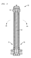
- FIG. 3 illustrates a diagram of an embodiment of a microelectromechanical switch constructed in accordance with the principles of the present invention.
- FIG. 1 illustrates a bi-directional microelectromechanical element 100 that contains a cold beam 110 , a first beam pair 120 , a second beam pair 130 , and a free end tether 140 .
- the cold beam 110 can have a variable width, i.e., a tapered beam or can have two or more sections with different widths.
- the cold beam 110 has a first end connected to a cold beam anchor 112 and a free end 114 .
- the free end 114 of the cold beam 110 is attached by conventional means to free end tether 140 .
- the cold beam anchor 112 is attached by conventional means to a substrate (not shown).
- the cold beam 110 is typically made of a metal such as nickel.
- a portion of the bi-directional microelectromechanical element 100 is located over a trench in the substrate (not shown).
- the second beam pair 130 is parallel to the cold beam 110 and is comprised of two parallel members, a third beam member 132 and a fourth beam member 134 , each having a first and second end.
- the first end of each parallel member is attached to an anchor.
- the first end of third beam member 132 is attached to a third anchor 136 and the first end of the fourth beam member 134 is attached to a fourth anchor 138 .
- Third anchor 136 and fourth anchor 138 are attached to the substrate by conventional means.
- the second ends of third beam member 132 and fourth beam member 134 are connected to form a closed loop.
- the connected second ends of third beam member 132 and fourth beam member 134 are conventionally attached to free end tether 140 .
- Both third beam member 132 and fourth beam member 134 are typically made of a metal such as nickel.
- beam pairs may not be parallel to a cold beam or to each other.
- beam members may have a variable width, i.e., a tapered beam member, may have two or more sections of different widths, or may have a different shape/configuration.
- the free end tether 140 mechanically couples: the free end 114 of the cold beam 110 ; the second ends of first beam member 122 and second beam member 124 of first beam pair 120 ; and the second ends of third beam member 132 and fourth beam member 134 of second beam pair 130 .
- the free end tether 140 is typically made of (often entirely made of) a dielectric material.
- the dielectric is a photoresist material such as “SU-8.”
- SU-8 is a negative, epoxy-type, near-UV photoresist based on EPON SU-8 epoxy resin (from Shell Chemical). It should be noted that other photoresists can be used as well, depending on design requirements.
- Other possible suitable materials include polyimide, spin on glass, or other polymers.
- Both the first beam pair 120 and second beam pair 130 may have a strain relief at the first end of one of the first 122 , second 124 , third 132 , or fourth 134 beam members.
- These strain reliefs decrease the stiffness of the first beam pair 120 and second beam pair 130 .
- a strain relief may be located or shaped differently or not be used.
- Each beam pair 120 , 130 can also include at least one beam pair tether deposited anywhere along beam pair 120 , 130 between beam member anchors 126 , 128 , 136 , 138 and free end tether 140 .
- FIG. 1 illustrates an embodiment where first beam pair 120 includes a beam pair tether 150 transversally disposed and deposited by conventional means at the first ends of the first beam member 122 and second beam member 124 .
- the embodiment of FIG. 1 also illustrates a beam pair tether 152 transversally disposed and conventionally deposited at the first ends of the third beam member 132 and fourth beam member 134 of the second beam pair 130 .
- the beam pair tethers 150 , 152 are dielectric tethers that are typically a photoresist as described above for the free end tether 140 .
- At least one additional tether 160 can be transversally disposed and conventionally deposited across the first beam pair 120 , cold beam 110 , and second beam member 130 and located between the free end tether 140 and the cold beam anchor 112 .
- the additional tether(s) is typically a photoresist as described above for the free end tether 140 and beam pair tethers 150 , 152 .
- Additional tether 160 mechanically couples the first beam pair 120 , cold beam 110 , and second beam pair 130 so that when deflected, they maintain their relative position to each other.
- Tip 170 is typically made of a conductive metal such as gold and is attached to the free end 114 of the cold beam 110 with conventional techniques.
- the tip 170 as illustrated in the embodiment of FIG. 1 , has a single prong 172 . In other embodiments, there could be more than one prong 172 at the end of the tip 170 .
- FIG. 2 illustrates an embodiment with a bi-directional microelectromechanical member 200 , which is the same as the bi-directional microelectromechanical member 100 of FIG. 1 .
- Bi-directional member 200 includes a cold beam 210 , a first beam pair 220 , a second beam pair 230 , and a free end tether 240 that mechanically couples the cold beam 210 , first beam pair 220 , and second beam pair 230 .
- the cold beam 210 , first beam pair 220 , and second beam pair 230 are conventionally attached to a substrate (not shown) via anchors as illustrated in the embodiment of FIG. 1 .
- the first beam pair 220 and the second beam pair 230 are configured to elongate when heated.
- the bi-directional member 200 When either beam pair is heated to a temperature greater than the cold beam 210 , the bi-directional member 200 , anchored at one end to the substrate, located above a trench in the substrate, and mechanically coupled by free end tether 240 , will deflect because the beam pair that is heated will expand greater than the cold beam 210 .
- the bi-directional member 200 when the first beam pair 220 is heated to a temperature greater than a temperature of the cold beam 210 and second beam pair 230 , the bi-directional member 200 will deflect in the direction shown by arrow 290 . Conversely, when second beam pair 230 is heated to a greater temperature than the cold beam 210 and first beam pair 220 , the bi-directional element 200 will deflect in the direction shown by arrow 280 . In the embodiments illustrated in FIGS. 1 and 2 , the heating of a beam pair is accomplished by applying current into one beam member of the beam pair and out of the other.
- bi-directional element 200 may be used an out-of-plane configuration wherein the deflection of the bi-directional element is either towards or away from the substrate.
- FIG. 3 illustrates an embodiment of a microelectromechanical switch 300 .
- the microelectromechanical switch 300 includes bi-directional element 302 , which is the bi-directional element 100 of the embodiment illustrated in FIG. 1 , and a unidirectional element 304 .
- the microelectromechanical switch 300 can be used to replace conventional microelectromechanical switches as presently employed.
- the microelectromechanical switch 300 includes the added functionality of two latch positions. Furthermore, the microelectromechanical switch 300 provides compensation for mechanical creep.
- unidirectional element 304 includes a cold beam 310 and a beam pair 320 .
- the cold beam 310 has a first end connected to a cold beam anchor 312 and a free end 314 .
- the free end 314 of the cold beam 310 is conventionally attached to a free end tether 340 .
- the cold beam anchor 312 is conventionally attached to a substrate (not shown).
- the cold beam 310 is typically made of a metal such as nickel.
- a portion of the unidirectional element 304 is located over a trench in the substrate (not shown).
- the free end tether 340 mechanically couples the free end 314 of the cold beam 310 and the second ends of first beam member 322 and second beam member 324 .
- the free end tether 340 is typically made up of a photoresist such as SU-8.
- the beam pair 320 may have a strain relief at the first end of one of the first beam member 322 or second beam member 324 (not shown). As with the strain reliefs 135 of the embodiment as illustrated in FIG. 1 , the strain relief (not shown) decreases the stiffness of the beam pair 320 .
- Beam pair 320 may include at least one beam pair tether 350 , transversally disposed and deposited by conventional means anywhere along beam pair 320 between beam member anchors 326 , 328 and free end tether 340 .
- the beam pair tether 350 is typically a photoresist as described above for the dielectric tether 340 .
- At least one additional tether 360 can be transversally disposed and conventionally deposited across beam pair 320 and cold beam 310 between the free end 314 of cold beam 310 and the cold beam anchor 312 .
- the additional tether(s) 360 is typically a photoresist as described above for the free end tether 340 .
- First tip 370 is typically made of a conductive metal such as gold and is attached to the free end 314 of the cold beam 310 with conventional techniques.
- the first tip 370 has two prongs 372 . In other embodiments, there could be a single prong 372 or multiple prongs 372 at the end of the first tip element 370 .
- the first tip element 370 is switchably couplable with a second tip element 376 of the bi-directional microelectromechanical element 302 .
- the beam pair 320 of the unidirectional element 304 is configured to elongate when heated.
- the unidirectional member 304 anchored at one end to the substrate, located above a trench in the substrate, and mechanically coupled by dielectric tether 340 , will deflect because the heated beam pair 320 will expand greater than the cold beam 310 .
- the unidirectional micromechanical member 304 will deflect away from the bi-directional element 302 .
- the heating of beam pair 320 is accomplished by applying current into the first beam member 322 of first beam pair 320 and out of second beam member 324 , causing beam pair 320 to heat and elongate.
- the bi-directional element 302 can be implemented in an out-of-plane configuration. In these embodiments, the bi-directional element 302 moves in a direction not parallel to the substrate but either towards or away from the substrate. For these embodiments, the bi-directional element 302 would not be switchably couplable to unidirectional element 304 but, rather, switched to contacts which can be in a different plane or planes. For example, the contacts may be in the substrate or in a layer or layers above the substrate. Also, in these embodiments, the mechanism to move a cold beam could, in addition to expansion from an adjacent, mechanically coupled heated beam pair, be another mechanism, such as an electrostatic or a capacitive mechanism.
- a bi-directional element constructed according to the present invention may be employed in an RF microelectromechanical switch as disclosed in an article in the December, 2001 IEEE Microwave Magazine entitled “RF MEMS Switches and Switch Circuits” by Gabriel M. Rebeiz, et al., which is incorporated herein by reference in its entirety.
- FIG. 4 illustrates an embodiment of a method to reduce creep in a microelectromechanical device with a bi-directional element 400 , carried out in accordance with the principles of the present invention.
- the method 400 begins in a step 405 with an intent to reduce creep in a microelectromechanical device with a bi-directional element.
- a current is applied to a unidirectional element of the microelectromechanical device to move the unidirectional element away from its initial position in step 410 .
- the current may be applied to a beam pair of the unidirectional element to move a cold beam of the unidirectional element from the initial position and away from the bi-directional element of the microelectromechanical device.
- current is then applied to the bi-directional element of the microelectromechanical device to move it in a first direction away from its initial position to a first position in step 415 .
- the current may be applied to a beam pair of the bi-directional element to move a cold beam of the bi-directional element from the initial position.
- the current to the unidirectional element is then terminated in step 420 allowing the unidirectional element to return to its initial position. This may be accomplished by removing the current from the beam pair of the unidirectional element.
- the current to the bi-directional element in the microelectromechanical device is terminated in step 425 . This may be accomplished by removing the current from the beam pair of the bi-directional element.
- the bi-directional element attempts to move back to its initial position.
- a prong of a tip of the unidirectional element prevents the bi-directional element from returning to its initial position by contacting a prong of a tip of the bi-directional element.
- the prong of the bi-directional element which was displaced when the current was applied, contacts the prong of the unidirectional element which prevents the bi-directional element from returning to is initial position. In this position, the bi-directional element is deformed and an electrical contact is formed between the unidirectional element and the bi-directional element.
- a microelectromechanical device such as a switch or relay may need to remain in a closed position for an extended period of time, on the order of weeks to months. It is known that metals under external forces for a sufficient time show a permanent deformation when the external force is removed resulting in mechanical creep. In a typical microelectromechanical device such as a switch or relay, the total distance a switch element must move to operate can be on the order of several microns. If the microelectromechanical device is held in one position for a sufficient period of time, misplacement of the switch element due to mechanical creep may be on the order of 3-4 microns and be great enough to render the microelectromechanical device inoperable.
- a predetermined time is established based on a maximum time to hold the bi-directional member in one position before rendering the microelectromechanical device inoperable.
- the method 400 proceeds to step 430 and determines if the microelectromechanical switch has remained in a position for the predetermined time.
- the predetermined time a bi-directional member of a microelectromechanical switch can be held in one position before deforming a sufficient amount that renders the microelectromechanical switch inoperable is based on historical data and many factors, such as, for example: the design of the microelectromechanical switch, e.g., the total distance the switch element must move, the material the bi-directional element and unidirectional element are comprised of, the dimensions of components of the bi-directional and unidirectional elements, etc.; and the ambient temperature of the microelectromechanical device.
- the design of the microelectromechanical switch e.g., the total distance the switch element must move, the material the bi-directional element and unidirectional element are comprised of, the dimensions of components of the bi-directional and unidirectional elements, etc.
- the ambient temperature of the microelectromechanical device One of ordinary skill in the art would understand there are other parameters that could aid in the determination of the maximum time to hold the bi-directional element in one position.
- a controller associated with the microelectromechanical switch may store or access the above-mentioned parameters associated with the microelectromechanical switch and decide when the predetermined time has occurred.
- the controller may be a conventional device electrically coupled to the unidirectional and bi-directional elements of the microelectromechanical switch.
- step 430 If, in the decisional step 430 , the switch has remained in one position for the predetermined time, the method moves on to step 435 where current is applied to the unidirectional element to move it away from its initial position and the bi-directional element. In some embodiments, a current can be applied to the bi-directional element to help break contact with the unidirectional element before moving to step 435 . If the switch has not remained in one position for the predetermined time, the method 400 returns to step 430 .
- step 440 current is applied in step 440 to move the bi-directional element in an opposite direction and to move a second prong of the tip element horizontally displaced opposite the first prong of the tip element beyond the prong of the unidirectional element.
- step 445 the current to the unidirectional element is terminated in step 445 allowing the unidirectional element to return to its initial position.
- the bi-directional element attempts to move back to its initial position. Again, the prong of the tip of the unidirectional element prevents the bi-directional element from returning to its initial position as the second prong of the tip element of the bi-directional element horizontally displaced opposite the first prong of the tip element of the bi-directional element contacts the prong of the tip element of the unidirectional element, stopping the movement of the bi-directional element. In this position, the bi-directional element is deformed in an opposite direction and will reverse the mechanical creep induced in the bi-directional member when in the previous position if held in place for a sufficient time. As before, the cold beam, tip, and prong of the bi-directional element and the cold beam, tip, and prong of the unidirectional element are electrically coupled and form a circuit which passes an electrical signal through the microelectromechanical device.
- the method 400 After moving the bi-directional element into an opposite position, the method 400 returns to step 430 and continues as before.
- Other configurations of the prongs of the tips of the unidirectional and bi-directional elements to accomplish the same reversal of mechanical creep induced from long-term deformations of the elements are within the scope of the invention but are not described here.
Abstract
Description
Claims (5)
Priority Applications (7)
| Application Number | Priority Date | Filing Date | Title |
|---|---|---|---|
| US11/772,039 US7760065B2 (en) | 2007-06-29 | 2007-06-29 | MEMS device with bi-directional element |
| PCT/US2008/007944 WO2009005683A1 (en) | 2007-06-29 | 2008-06-26 | A mems device with bi-directional element |
| EP08779783A EP2162894A1 (en) | 2007-06-29 | 2008-06-26 | A mems device with bi-directional element |
| JP2010514810A JP2010532276A (en) | 2007-06-29 | 2008-06-26 | MEMS device having bidirectional element |
| KR1020097027214A KR20100041710A (en) | 2007-06-29 | 2008-06-26 | A mems device with bi-directional element |
| CN200880022718A CN101689438A (en) | 2007-06-29 | 2008-06-26 | MEMS device with bilateral element |
| US12/732,752 US7973637B2 (en) | 2007-06-29 | 2010-03-26 | MEMS device with bi-directional element |
Applications Claiming Priority (1)
| Application Number | Priority Date | Filing Date | Title |
|---|---|---|---|
| US11/772,039 US7760065B2 (en) | 2007-06-29 | 2007-06-29 | MEMS device with bi-directional element |
Related Child Applications (1)
| Application Number | Title | Priority Date | Filing Date |
|---|---|---|---|
| US12/732,752 Division US7973637B2 (en) | 2007-06-29 | 2010-03-26 | MEMS device with bi-directional element |
Publications (2)
| Publication Number | Publication Date |
|---|---|
| US20090002118A1 US20090002118A1 (en) | 2009-01-01 |
| US7760065B2 true US7760065B2 (en) | 2010-07-20 |
Family
ID=39773076
Family Applications (2)
| Application Number | Title | Priority Date | Filing Date |
|---|---|---|---|
| US11/772,039 Expired - Fee Related US7760065B2 (en) | 2007-06-29 | 2007-06-29 | MEMS device with bi-directional element |
| US12/732,752 Expired - Fee Related US7973637B2 (en) | 2007-06-29 | 2010-03-26 | MEMS device with bi-directional element |
Family Applications After (1)
| Application Number | Title | Priority Date | Filing Date |
|---|---|---|---|
| US12/732,752 Expired - Fee Related US7973637B2 (en) | 2007-06-29 | 2010-03-26 | MEMS device with bi-directional element |
Country Status (6)
| Country | Link |
|---|---|
| US (2) | US7760065B2 (en) |
| EP (1) | EP2162894A1 (en) |
| JP (1) | JP2010532276A (en) |
| KR (1) | KR20100041710A (en) |
| CN (1) | CN101689438A (en) |
| WO (1) | WO2009005683A1 (en) |
Cited By (4)
| Publication number | Priority date | Publication date | Assignee | Title |
|---|---|---|---|---|
| US20060238279A1 (en) * | 2005-03-18 | 2006-10-26 | Simpler Networks Inc. | Mems actuators and switches |
| US20110006874A1 (en) * | 2008-02-26 | 2011-01-13 | Nb Technologies Gmbh | Micromechanical actuator |
| US20110063068A1 (en) * | 2009-09-17 | 2011-03-17 | The George Washington University | Thermally actuated rf microelectromechanical systems switch |
| US11536872B2 (en) * | 2012-11-16 | 2022-12-27 | Stmicroelectronics (Rousset) Sas | Method for producing an integrated circuit pointed element comprising etching first and second etchable materials with a particular etchant to form an open crater in a project |
Families Citing this family (4)
| Publication number | Priority date | Publication date | Assignee | Title |
|---|---|---|---|---|
| US20090033454A1 (en) * | 2007-08-01 | 2009-02-05 | Simpler Networks Inc. | MEMS actuators with even stress distribution |
| DE102007052048A1 (en) * | 2007-10-31 | 2009-05-14 | Advanced Micro Devices, Inc., Sunnyvale | Double integration scheme for low resistance metal layer |
| EP2749890A1 (en) * | 2012-12-27 | 2014-07-02 | Nederlandse Organisatie voor toegepast -natuurwetenschappelijk onderzoek TNO | A composite beam having an adjustable stiffness. |
| US9153483B2 (en) * | 2013-10-30 | 2015-10-06 | Taiwan Semiconductor Manufacturing Company, Ltd. | Method of semiconductor integrated circuit fabrication |
Citations (14)
| Publication number | Priority date | Publication date | Assignee | Title |
|---|---|---|---|---|
| US6268635B1 (en) * | 1999-08-04 | 2001-07-31 | Jds Uniphase Inc. | Dielectric links for microelectromechanical systems |
| US6407478B1 (en) * | 2000-08-21 | 2002-06-18 | Jds Uniphase Corporation | Switches and switching arrays that use microelectromechanical devices having one or more beam members that are responsive to temperature |
| US6608714B2 (en) * | 2001-06-28 | 2003-08-19 | Southwest Research Institute | Bi-directional, single material thermal actuator |
| US6624730B2 (en) * | 2000-03-28 | 2003-09-23 | Tini Alloy Company | Thin film shape memory alloy actuated microrelay |
| US6679055B1 (en) * | 2002-01-31 | 2004-01-20 | Zyvex Corporation | Electrothermal quadmorph microactuator |
| US6708491B1 (en) * | 2000-09-12 | 2004-03-23 | 3M Innovative Properties Company | Direct acting vertical thermal actuator |
| US6904191B2 (en) * | 2003-03-19 | 2005-06-07 | Xerox Corporation | MXN cantilever beam optical waveguide switch |
| US7036312B2 (en) * | 2003-04-22 | 2006-05-02 | Simpler Networks, Inc. | MEMS actuators |
| US20060238279A1 (en) | 2005-03-18 | 2006-10-26 | Simpler Networks Inc. | Mems actuators and switches |
| US20070096860A1 (en) | 2005-11-02 | 2007-05-03 | Innovative Micro Technology | Compact MEMS thermal device and method of manufacture |
| US20070215448A1 (en) * | 2006-03-20 | 2007-09-20 | Innovative Micro Technology | MEMS thermal device with slideably engaged tether and method of manufacture |
| US20080087530A1 (en) * | 2006-10-12 | 2008-04-17 | Innovative Micro Technology | Contact electrode for microdevices and etch method of manufacture |
| US20080197964A1 (en) * | 2007-02-21 | 2008-08-21 | Simpler Networks Inc. | Mems actuators and switches |
| US7548145B2 (en) * | 2006-01-19 | 2009-06-16 | Innovative Micro Technology | Hysteretic MEMS thermal device and method of manufacture |
Family Cites Families (1)
| Publication number | Priority date | Publication date | Assignee | Title |
|---|---|---|---|---|
| US6718764B1 (en) * | 2002-06-28 | 2004-04-13 | Zyvex Corporation | System and method for microstructure positioning using metal yielding |
-
2007
- 2007-06-29 US US11/772,039 patent/US7760065B2/en not_active Expired - Fee Related
-
2008
- 2008-06-26 CN CN200880022718A patent/CN101689438A/en active Pending
- 2008-06-26 EP EP08779783A patent/EP2162894A1/en not_active Withdrawn
- 2008-06-26 WO PCT/US2008/007944 patent/WO2009005683A1/en active Application Filing
- 2008-06-26 KR KR1020097027214A patent/KR20100041710A/en not_active Application Discontinuation
- 2008-06-26 JP JP2010514810A patent/JP2010532276A/en active Pending
-
2010
- 2010-03-26 US US12/732,752 patent/US7973637B2/en not_active Expired - Fee Related
Patent Citations (15)
| Publication number | Priority date | Publication date | Assignee | Title |
|---|---|---|---|---|
| US6268635B1 (en) * | 1999-08-04 | 2001-07-31 | Jds Uniphase Inc. | Dielectric links for microelectromechanical systems |
| US7084726B2 (en) * | 2000-03-28 | 2006-08-01 | Tini Alloy Company | Thin film shape memory alloy actuated microrelay |
| US6624730B2 (en) * | 2000-03-28 | 2003-09-23 | Tini Alloy Company | Thin film shape memory alloy actuated microrelay |
| US6407478B1 (en) * | 2000-08-21 | 2002-06-18 | Jds Uniphase Corporation | Switches and switching arrays that use microelectromechanical devices having one or more beam members that are responsive to temperature |
| US6708491B1 (en) * | 2000-09-12 | 2004-03-23 | 3M Innovative Properties Company | Direct acting vertical thermal actuator |
| US6608714B2 (en) * | 2001-06-28 | 2003-08-19 | Southwest Research Institute | Bi-directional, single material thermal actuator |
| US6679055B1 (en) * | 2002-01-31 | 2004-01-20 | Zyvex Corporation | Electrothermal quadmorph microactuator |
| US6904191B2 (en) * | 2003-03-19 | 2005-06-07 | Xerox Corporation | MXN cantilever beam optical waveguide switch |
| US7036312B2 (en) * | 2003-04-22 | 2006-05-02 | Simpler Networks, Inc. | MEMS actuators |
| US20060238279A1 (en) | 2005-03-18 | 2006-10-26 | Simpler Networks Inc. | Mems actuators and switches |
| US20070096860A1 (en) | 2005-11-02 | 2007-05-03 | Innovative Micro Technology | Compact MEMS thermal device and method of manufacture |
| US7548145B2 (en) * | 2006-01-19 | 2009-06-16 | Innovative Micro Technology | Hysteretic MEMS thermal device and method of manufacture |
| US20070215448A1 (en) * | 2006-03-20 | 2007-09-20 | Innovative Micro Technology | MEMS thermal device with slideably engaged tether and method of manufacture |
| US20080087530A1 (en) * | 2006-10-12 | 2008-04-17 | Innovative Micro Technology | Contact electrode for microdevices and etch method of manufacture |
| US20080197964A1 (en) * | 2007-02-21 | 2008-08-21 | Simpler Networks Inc. | Mems actuators and switches |
Non-Patent Citations (8)
| Title |
|---|
| Agrawal, A Latching MEMS Relay for DC and RF Applications, IEEE, 8.2, pp. 222-225. |
| Larsen, et al. "MEMS device for bending test: measurements of fatigue and creep of electroplated nickel;" Sensors and Actuators; A 103; Jan. 2003; pp. 156-164. |
| Modlinski, et al. "Creep as a reliability problem in MEMS;" Microelectronics Reliability, vol. 44; Sep. 2004; pp. 1733-1738. |
| Modlinski, et al. "Creep-resistant aluminum alloys for use in MEMS;" Journal of Micromechanics and Microengineering; vol. 15; Jul. 2005; pp. S165-S170. |
| PCT International Search Report and PCT Written Opinion of the International Searching Authority, Oct. 2008. |
| PCT International Search Report and PCT Written Opinion of the International Searching Authority. |
| Rebeiz, et al., RF MEMS Switches and Switch Circuits, IEEE Microwave Magazine, Dec. 2001, pp. 59-71. |
| Vickers-Kirby, et al. "Anelastic Creep Phenomena in Thin Metal Plated Cantilevers for MEMS;" Materials Research Society Symposium Proceedings; vol. 657; Nov. 2001; pp. EE2.5.1-EE2.5.6. |
Cited By (5)
| Publication number | Priority date | Publication date | Assignee | Title |
|---|---|---|---|---|
| US20060238279A1 (en) * | 2005-03-18 | 2006-10-26 | Simpler Networks Inc. | Mems actuators and switches |
| US8115576B2 (en) * | 2005-03-18 | 2012-02-14 | Réseaux MEMS, Société en commandite | MEMS actuators and switches |
| US20110006874A1 (en) * | 2008-02-26 | 2011-01-13 | Nb Technologies Gmbh | Micromechanical actuator |
| US20110063068A1 (en) * | 2009-09-17 | 2011-03-17 | The George Washington University | Thermally actuated rf microelectromechanical systems switch |
| US11536872B2 (en) * | 2012-11-16 | 2022-12-27 | Stmicroelectronics (Rousset) Sas | Method for producing an integrated circuit pointed element comprising etching first and second etchable materials with a particular etchant to form an open crater in a project |
Also Published As
| Publication number | Publication date |
|---|---|
| WO2009005683A1 (en) | 2009-01-08 |
| US20090002118A1 (en) | 2009-01-01 |
| JP2010532276A (en) | 2010-10-07 |
| EP2162894A1 (en) | 2010-03-17 |
| KR20100041710A (en) | 2010-04-22 |
| WO2009005683A8 (en) | 2010-01-28 |
| US7973637B2 (en) | 2011-07-05 |
| CN101689438A (en) | 2010-03-31 |
| US20100182120A1 (en) | 2010-07-22 |
Similar Documents
| Publication | Publication Date | Title |
|---|---|---|
| US7973637B2 (en) | MEMS device with bi-directional element | |
| US20050189204A1 (en) | Microengineered broadband electrical switches | |
| CN101147223B (en) | RF MEMS switch with a flexible and free switch membrane | |
| US7471176B2 (en) | Micro electromechanical system switch | |
| EP2073236B1 (en) | MEMS Microswitch having a conductive mechanical stop | |
| US20050146404A1 (en) | Microengineered self-releasing switch | |
| US7692519B2 (en) | MEMS switch with improved standoff voltage control | |
| EP1412282A2 (en) | Multi-directional thermal actuator | |
| US20060114084A1 (en) | Latching micro-magnetic switch with improved thermal reliability | |
| EP2200063A2 (en) | Micro-electromechanical system switch | |
| US8528885B2 (en) | Multi-stage spring system | |
| Cao et al. | Bi-directional electrothermal electromagnetic actuators | |
| US20110012703A1 (en) | Mems actuators and switches | |
| US8232858B1 (en) | Microelectromechanical (MEM) thermal actuator | |
| EP2126942B1 (en) | Mems actuators and switches | |
| KR20110113977A (en) | Switching element and switching circuit responding to acceleration | |
| EP2168908A1 (en) | Micromechanical thermal actuator | |
| Shuaibu et al. | Toward a polysilicon-based electrostatically actuated DC MEMS switch | |
| Oberhammer et al. | Mechanically tri-stable in-line single-pole-double-throw all-metal switch | |
| Nage et al. | A Non-Contact Type Comb Drive for the Removal of Stiction Mechanism in MEMS Switch | |
| KR20050102073A (en) | Microfabricated relay with multimorph actuator and electrostatic latch mechanism |
Legal Events
| Date | Code | Title | Description |
|---|---|---|---|
| AS | Assignment |
Owner name: ALCATEL-LUCENT, NEW JERSEY Free format text: ASSIGNMENT OF ASSIGNORS INTEREST;ASSIGNORS:GASPARYAN, ARMAN;GATES, JOHN VANATTA, II;SIMON, MARIA ELINA;REEL/FRAME:019502/0044 Effective date: 20070629 |
|
| FEPP | Fee payment procedure |
Free format text: PAYOR NUMBER ASSIGNED (ORIGINAL EVENT CODE: ASPN); ENTITY STATUS OF PATENT OWNER: LARGE ENTITY |
|
| AS | Assignment |
Owner name: LUCENT TECHNOLOGIES INC.,NEW JERSEY Free format text: CORRECTIVE ASSIGNMENT TO CORRECT THE ASSIGNEE NAME PREVIOUSLY RECORDED ON REEL 019502 FRAME 0044. ASSIGNOR(S) HEREBY CONFIRMS THE ASSIGNEE ALCATEL-LUCENT IS INCORRECT IT SHOULD READ LUCENT TECHNOLOGIES INC.;ASSIGNORS:GASPARYAN, ARMAN;GATES II, JOHN VANATTA;SIMON, MARIA ELINA;REEL/FRAME:024328/0571 Effective date: 20070629 Owner name: LUCENT TECHNOLOGIES INC., NEW JERSEY Free format text: CORRECTIVE ASSIGNMENT TO CORRECT THE ASSIGNEE NAME PREVIOUSLY RECORDED ON REEL 019502 FRAME 0044. ASSIGNOR(S) HEREBY CONFIRMS THE ASSIGNEE ALCATEL-LUCENT IS INCORRECT IT SHOULD READ LUCENT TECHNOLOGIES INC.;ASSIGNORS:GASPARYAN, ARMAN;GATES II, JOHN VANATTA;SIMON, MARIA ELINA;REEL/FRAME:024328/0571 Effective date: 20070629 |
|
| AS | Assignment |
Owner name: ALCATEL-LUCENT USA INC.,NEW JERSEY Free format text: MERGER;ASSIGNOR:LUCENT TECHNOLOGIES INC.;REEL/FRAME:024470/0583 Effective date: 20081101 Owner name: ALCATEL-LUCENT USA INC., NEW JERSEY Free format text: MERGER;ASSIGNOR:LUCENT TECHNOLOGIES INC.;REEL/FRAME:024470/0583 Effective date: 20081101 |
|
| STCF | Information on status: patent grant |
Free format text: PATENTED CASE |
|
| FPAY | Fee payment |
Year of fee payment: 4 |
|
| AS | Assignment |
Owner name: OMEGA CREDIT OPPORTUNITIES MASTER FUND, LP, NEW YORK Free format text: SECURITY INTEREST;ASSIGNOR:WSOU INVESTMENTS, LLC;REEL/FRAME:043966/0574 Effective date: 20170822 Owner name: OMEGA CREDIT OPPORTUNITIES MASTER FUND, LP, NEW YO Free format text: SECURITY INTEREST;ASSIGNOR:WSOU INVESTMENTS, LLC;REEL/FRAME:043966/0574 Effective date: 20170822 |
|
| AS | Assignment |
Owner name: WSOU INVESTMENTS, LLC, CALIFORNIA Free format text: ASSIGNMENT OF ASSIGNORS INTEREST;ASSIGNOR:ALCATEL LUCENT;REEL/FRAME:044000/0053 Effective date: 20170722 |
|
| FEPP | Fee payment procedure |
Free format text: MAINTENANCE FEE REMINDER MAILED (ORIGINAL EVENT CODE: REM.) |
|
| FEPP | Fee payment procedure |
Free format text: 7.5 YR SURCHARGE - LATE PMT W/IN 6 MO, LARGE ENTITY (ORIGINAL EVENT CODE: M1555) |
|
| MAFP | Maintenance fee payment |
Free format text: PAYMENT OF MAINTENANCE FEE, 8TH YEAR, LARGE ENTITY (ORIGINAL EVENT CODE: M1552) Year of fee payment: 8 |
|
| AS | Assignment |
Owner name: BP FUNDING TRUST, SERIES SPL-VI, NEW YORK Free format text: SECURITY INTEREST;ASSIGNOR:WSOU INVESTMENTS, LLC;REEL/FRAME:049235/0068 Effective date: 20190516 |
|
| AS | Assignment |
Owner name: WSOU INVESTMENTS, LLC, CALIFORNIA Free format text: RELEASE BY SECURED PARTY;ASSIGNOR:OCO OPPORTUNITIES MASTER FUND, L.P. (F/K/A OMEGA CREDIT OPPORTUNITIES MASTER FUND LP;REEL/FRAME:049246/0405 Effective date: 20190516 |
|
| AS | Assignment |
Owner name: OT WSOU TERRIER HOLDINGS, LLC, CALIFORNIA Free format text: SECURITY INTEREST;ASSIGNOR:WSOU INVESTMENTS, LLC;REEL/FRAME:056990/0081 Effective date: 20210528 |
|
| AS | Assignment |
Owner name: WSOU INVESTMENTS, LLC, CALIFORNIA Free format text: RELEASE BY SECURED PARTY;ASSIGNOR:TERRIER SSC, LLC;REEL/FRAME:056526/0093 Effective date: 20210528 |
|
| FEPP | Fee payment procedure |
Free format text: MAINTENANCE FEE REMINDER MAILED (ORIGINAL EVENT CODE: REM.); ENTITY STATUS OF PATENT OWNER: LARGE ENTITY |
|
| LAPS | Lapse for failure to pay maintenance fees |
Free format text: PATENT EXPIRED FOR FAILURE TO PAY MAINTENANCE FEES (ORIGINAL EVENT CODE: EXP.); ENTITY STATUS OF PATENT OWNER: LARGE ENTITY |
|
| STCH | Information on status: patent discontinuation |
Free format text: PATENT EXPIRED DUE TO NONPAYMENT OF MAINTENANCE FEES UNDER 37 CFR 1.362 |
|
| FP | Lapsed due to failure to pay maintenance fee |
Effective date: 20220720 |