US7765420B2 - Single-wire sequencing technique - Google Patents
Single-wire sequencing technique Download PDFInfo
- Publication number
- US7765420B2 US7765420B2 US11/208,630 US20863005A US7765420B2 US 7765420 B2 US7765420 B2 US 7765420B2 US 20863005 A US20863005 A US 20863005A US 7765420 B2 US7765420 B2 US 7765420B2
- Authority
- US
- United States
- Prior art keywords
- slave
- sequencing
- signal
- event
- circuit
- Prior art date
- Legal status (The legal status is an assumption and is not a legal conclusion. Google has not performed a legal analysis and makes no representation as to the accuracy of the status listed.)
- Active, expires
Links
Images


Classifications
-
- G—PHYSICS
- G06—COMPUTING; CALCULATING OR COUNTING
- G06F—ELECTRIC DIGITAL DATA PROCESSING
- G06F1/00—Details not covered by groups G06F3/00 - G06F13/00 and G06F21/00
- G06F1/16—Constructional details or arrangements
- G06F1/18—Packaging or power distribution
- G06F1/189—Power distribution
Definitions
- This disclosure relates to sequencers, and more particularly, to circuitry and methodology for sequencing events that require different amounts of time to complete.
- Sequencers are devices for automatically determining and controlling sequences of events, such as turning on or turning off power supplies.
- Many Application-Specific Integration Circuits (ASICs), microprocessors and other electronic circuits require multiple power supplies in order to operate. Often, these power supplies must be turned on and off in a specific order to avoid damage to an electronic circuit or to enable an electronic circuit to operate in a proper manner. Also, it may be desirable to initiate turning on one or several power supplies at a particular time slot and wait until these power supplies are on before turning on the next power supply or the next group of power supplies.
- ASICs Application-Specific Integration Circuits
- microprocessors microprocessors
- other electronic circuits require multiple power supplies in order to operate. Often, these power supplies must be turned on and off in a specific order to avoid damage to an electronic circuit or to enable an electronic circuit to operate in a proper manner. Also, it may be desirable to initiate turning on one or several power supplies at a particular time slot and wait until these power supplies are on before turning on the next power supply or
- sequencing must involve multiple electronic circuits at different locations on an electronic assembly or at different electronic assemblies. Therefore, to perform sequencing, electrical communications between electronic circuits must be provided.
- One way to coordinate multiple electronic circuits involved in sequencing is to provide a central or master circuit that has multiple control outputs and status inputs for each sequenced event.
- Another solution might be to use a serial communication protocol, such as 12C, with an intelligent master controller.
- serial communication protocol such as 12C
- most communications protocols would not support highly accurate timing of events.
- the sequencing system comprises a master circuit for providing sequencing information defining a sequence of events using a sequencing signal, and at least one slave circuit responsive to the sequencing signal for producing at least one event signal defining an event.
- the master and slave circuits are configured for providing a bidirectional transfer of the sequencing information via a single wire.
- the sequencing information transferred from the master circuit to the slave circuit may define a required sequence of events, whereas the information transferred from the slave circuit to the master circuit indicates when the requested event is completed and enables the system to provide sequencing of events that require different amount of time to complete.
- Each slave circuit may be provided on a separate chip and comprise a plurality of slave channels for producing respective event signals during time slots assigned to the slave channels. Multiple slave channels may produce the event signals during the same time slot. Alternatively, no slave channels may operate during some of the time slots. The slave channel may monitor an event initiated during the assigned time slot to indicate to the master circuit that the event occurs.
- the slave circuit may comprise a counter common for the plurality of the slave channels and responsive to the sequencing signal for producing a count representing a time slot.
- Each slave channel may comprise a comparator for comparing the count with a predetermined value assigned to a particular slave channel to produce an event signal if the count corresponds to the predetermined value.
- the counter may be incremented or decremented in accordance with an external signal to represent multiple time slots for carrying out a required sequence of events.
- the master circuit may produce multiple sequencing signals defining a predetermined number of time slots in a particular sequence of events.
- a sequencing protocol may involve producing multiple sequencing signals for defining multiple time slots for carrying out a sequence of events, and producing multiple event signals defining respective events during a particular time slot.
- the sequencer is provided for controlling multiple power supplies in a power supply system.
- the sequencing procedure may be performed in two directions depending on a command from a system controller. For example, in one direction, multiple power supplies may be turned on in a predetermined order, and in the other direction, the power supplies may be turned off in the opposite order.
- FIG. 1 is a block-diagram of a sequencing system of the present disclosure.
- FIG. 2 is a diagram illustrating multiple channels in a slave sequenced event controller (SEC).
- SEC slave sequenced event controller
- FIG. 3 is a diagram illustrating a power supply incorporating slave SEC circuitry.
- FIG. 4 is a diagram illustrating the structure of a master SEC.
- FIG. 5 is a diagram illustrating the structure of the slave SEC.
- FIG. 1 shows a sequencing system 10 of the present disclosure that comprises a master sequenced event controller (SEC) 12 and slave SECs 14 , each of which is provided for controlling and monitoring one or more events.
- SEC master sequenced event controller
- FIG. 1 shows multiple slave SECs 14 , one skilled in the art would realize that only a single slave SEC 14 may be provided.
- each slave SEC 14 may control and monitor a group of power supplies 16 coupled to the respective slave SEC 14 .
- Master SEC 12 and the slave SECs 14 are connected with each other via a single-wire sequence control net (SCN) line that transfers SCN signals.
- SCN single-wire sequence control net
- the SCN line provides a bi-directional transfer of sequencing information between the master SEC 12 and slave SECs 14 . This transfer provides sequencing of events that require different time to complete.
- the master SEC 12 may interact with a system controller 18 that supplies an on/off signal to the master SEC 12 and each of the slave SECs 14 to conduct the sequencing procedure in two directions.
- the on-state of the on/off signal may result in turning on multiple power supplies in a predetermined order, and the off-state may initiate turning off the power supplies in the opposite order.
- the on/off signal may be a signal in which the on-state is inversed with respect to the off-state. For example, a high level of the on/off signal may correspond to the on-state and a low level of the same signal may correspond to the off-state.
- the master SEC 12 may supply the system controller 18 with a DONE signal, when the sequencing procedure is complete.
- Each slave SEC 14 may be arranged on a separate chip to control the respective group of power supplies 16 associated with this chip.
- the master SEC 12 and at least one of the slave SECs 14 may be provided on the same chip. Alternatively, they may be arranged on separate chips.
- each slave SEC 14 comprises multiple SEC slave (SCSS) channels 1 to n connected to respective power supplies 20 - 1 to 20 -n for controlling and monitoring the power supply.
- Each slave channel transmits an enable signal EN to control the respective power supply 20 , and receives a monitoring signal MON indicating a status or a monitored parameter of the respective power supply 20 .
- the slave channel 1 supplies a power supply 1 with an enable signal EN 1 and receives a monitoring signal MON 1 from the power supply 1 .
- the slave channel 2 supplies a power supply 2 with an enable signal EN 2 and receives a monitoring signal MON 2 from the power supply 2 .
- the slave channel n supplies a power supply n with an enable signal ENn and receives a monitoring signal MONn from this power supply.
- Each slave channel is configured to turn on in a particular time slot.
- an external configuration resistor Rswt may be provided for each slave channel to define a particular time slot.
- a configuration resistor Rswt 1 is provided to define a time slot for the slave channel 1
- a configuration resistor Rswt 2 is provided to define a time slot for the slave channel 2
- a configuration resistor Rswt(n) is arranged to define a time slot for the slave channel n.
- the configuration resistors Rswt for several slave channels may have the same value to turn on the respective slave channels in the same time slot.
- a power supply 22 may contain required circuitry for direct connection to the master SEC 12 .
- the power supply 22 is directly connected to the master SEC 12 via a bi-directional single-wire SCN line that transfers SCN signals.
- each power supply 22 may be directly supplied with the on/off signal from the system controller 18 to initiate turning on or off of the corresponding power supply 22 .
- Each power supply 22 may have a respective external configuration resistor Rswt to define a particular time slot for controlling the corresponding power supply 22 .
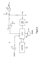
- the master SEC 12 comprises a counter 102 , a logic circuit 104 , a one-shot circuit 106 , a switching circuit 108 , a comparator 110 , an on/off signal pad 112 , an SCN pad 114 and a DONE signal pad 116 .
- the logic circuit 104 fires the one-shot circuit 106 producing a signal that turns on the switching circuit 108 .
- the signal SCN normally pulled high by a current source I R is pulled low.
- the signal SCN goes low, it defines the beginning of a time slot of a sequencing procedure.
- the signal SCN is pulled low until the slave SECs 14 carry out control operations scheduled during a particular time slot.
- the slave SECs 14 release the SCN line indicating that control operations scheduled during the current time slot are completed, the SCN signal goes high.
- the comparator 110 compares the SCN signal with a pre-set reference level V R and produces an output signal supplied to the logic circuit 104 when the SCN signal reaches the reference level. In response, after a predetermined delay, the logic circuit 104 fires the one-shot circuit 106 to initiate the next time slot.
- the counter 102 defines a predetermined number of time slots in a sequencing procedure. It counts the number of produced time slots and provides the logic circuit 104 with a signal terminating the sequencing procedure when the predetermined number of time slots is produced. In response to this signal, the logic circuit 104 issues the signal DONE supplied to the system controller 18 to report that the requested sequencing procedure is completed.
- each slave SEC 14 may comprise multiple SCSS channels and circuitry common for the SCSS channels.
- the common circuitry includes a logic circuit 202 , a counter 204 , a comparator 206 , an on/off signal pad 208 and an SCN pad 210 .
- Each SCSS channel includes a comparator 212 , a logic circuit 214 , a comparator 216 , an analog-to-digital converter (ADC) 218 , a switching circuit 220 , pads 222 , 224 and 226 , and a resistor Rswt.
- ADC analog-to-digital converter
- the comparator 206 compares the SCN signal with a predetermined threshold voltage V TH1 to increment or decrement the counter 204 .
- the SCN signal becomes lower than the threshold voltage V TH1 , and the comparator 206 produces a signal that increments or decrements the counter 204 .
- the direction of the counter 204 is controlled by the logic circuit 202 supplied with the on/off signal from the system controller 18 to switch the counter 204 into an incrementing mode when the on/off signal is in an on-state, and to switch the counter 204 into a decrementing mode when the on/off signal is in an off-state.
- the counter 204 In response to a low level of the SCN signal, the counter 204 is incremented or decremented to produce an N-digit count having a particular digital value. This count is supplied to the comparator 212 of each SCSS channel.
- the comparator 212 compares the N-digit count with an N-digit value produced by the ADC 218 based on an analog value defined by the resistor Rswt assigned to the SCSS channel. As discussed above, the value determined by the resistor Rswt defines a time slot, during which a particular SCSS channel is activated.
- the comparator 212 produces a signal that causes the logic circuit 214 to generate the enable signal EN supplied to the respective power supply 20 .
- each SCSS channel monitors the count of the counter 204 and produces the enable signal EN when the count corresponds to the time slot assigned to the respective SCSS channel.
- the logic circuit 214 produces a control signal to turn-on the switching circuit 220 in order to keep the SCN signal at a low level.
- the enable signal EN may be provided to the power supply 20 to turn it on or off. For example, when the on/off signal is in an on-state the enable signal EN may be produced to turn on the power supply 20 , and when the on/off signal is in an off-state, the enable signal EN may be supplied to turn off the power supply 20 .
- the SCSS channel may monitor the power supply 20 to determine whether the requested operation is fulfilled.
- the comparator 216 compares the monitoring signal MON received from the power supply 20 with a predetermined threshold voltage V TH2 corresponding to a required power level and produces an output signal supplied to the logic circuit 214 when the monitoring signal MON reaches the threshold voltage V TH2 .
- the monitoring signal MON may correspond to output voltage produced by the power supply 20 .
- the comparator 216 supplies the logic circuit 214 with an output signal, when the monitoring signal MON becomes zero or less than a predetermined threshold voltage indicating that the power is removed.
- the logic circuit 214 In response to the output signal of the comparator 216 , the logic circuit 214 produces a control signal to turn off the switching circuit 220 .
- Multiple SCSS channels may operate in a given time slot. When the last SCSS channel operating in a particular time slot determines that power from the corresponding power supply 20 is supplied or removed, it turns off its switching circuit 220 , releasing the SCN line and causing the SCN signal to go high.
- the predetermined threshold voltages may be selected depending on parameters of the power supply 20 controlled by a particular SCSS channel, and may differ for different SCSS channels.
- the master SEC 12 when the SCN line is pulled high, the master SEC 12 after a predetermined delay initiates the next time slot of the sequencing procedure by pulling the SCN line low. During the next time slot, one or more SCSS channels assigned to that time slot produce the enable signal EN to turn on or off power from the respective power supplies 20 . Alternatively, no SCSS channels may be assigned to a particular time slot. In this case, after a predetermined delay, the master SEC 12 initiates the next time slot. The sequencing procedure is continued until all time slots defined by the master SEC 12 are completed.
- the sequencing system of the present disclosure is able to sequentially control multiple power supplies associated with various chips using a single-wire SCN line that provides bidirectional transfer of sequencing information between master and slave SECs.
- the sequencing information transferred from the master circuit to the slave circuit may define a required sequence of events, whereas the information transferred from the slave circuit to the master circuit indicates when the requested event is completed and enables the system to provide sequencing of events that require different amount of time to complete.
Abstract
Description
Claims (21)
Priority Applications (2)
| Application Number | Priority Date | Filing Date | Title |
|---|---|---|---|
| US11/208,630 US7765420B2 (en) | 2005-08-23 | 2005-08-23 | Single-wire sequencing technique |
| TW095124197A TWI376593B (en) | 2005-08-23 | 2006-07-03 | Single-wire sequencing technique |
Applications Claiming Priority (1)
| Application Number | Priority Date | Filing Date | Title |
|---|---|---|---|
| US11/208,630 US7765420B2 (en) | 2005-08-23 | 2005-08-23 | Single-wire sequencing technique |
Publications (2)
| Publication Number | Publication Date |
|---|---|
| US20070050655A1 US20070050655A1 (en) | 2007-03-01 |
| US7765420B2 true US7765420B2 (en) | 2010-07-27 |
Family
ID=37805768
Family Applications (1)
| Application Number | Title | Priority Date | Filing Date |
|---|---|---|---|
| US11/208,630 Active 2028-05-08 US7765420B2 (en) | 2005-08-23 | 2005-08-23 | Single-wire sequencing technique |
Country Status (2)
| Country | Link |
|---|---|
| US (1) | US7765420B2 (en) |
| TW (1) | TWI376593B (en) |
Cited By (1)
| Publication number | Priority date | Publication date | Assignee | Title |
|---|---|---|---|---|
| US20220390998A1 (en) * | 2021-06-02 | 2022-12-08 | Infineon Technologies Ag | Adaptive host bus power control |
Families Citing this family (3)
| Publication number | Priority date | Publication date | Assignee | Title |
|---|---|---|---|---|
| US20100185881A1 (en) * | 2009-01-21 | 2010-07-22 | Kabushiki Kaisha Toshiba | Semiconductor device incorporating regulator and electric apparatus including a plurality of the semiconductor devices |
| JP2012038401A (en) * | 2010-08-11 | 2012-02-23 | Elpida Memory Inc | Semiconductor device and power supply control method for semiconductor device |
| US11374486B2 (en) * | 2020-09-29 | 2022-06-28 | Monolithic Power Systems, Inc. | Power supply with flexible control and the method thereof |
Citations (10)
| Publication number | Priority date | Publication date | Assignee | Title |
|---|---|---|---|---|
| US5237322A (en) * | 1990-12-08 | 1993-08-17 | Deutsche Itt Industries Gmbh | Master-slave data transmission system employing a flexible single-wire bus |
| US5343472A (en) * | 1990-03-30 | 1994-08-30 | Mazda Motor Corporation | Multiplex transmission system for use in vehicles |
| US6278713B1 (en) * | 1995-04-21 | 2001-08-21 | Illinois Institute Of Technology | Method and apparatus for distributed queue digital data transmission employing variable length data slots |
| US6298066B1 (en) * | 1999-04-14 | 2001-10-02 | Maxim Integrated Products, Inc. | Single wire bus interface for multidrop applications |
| US6473857B1 (en) * | 1999-12-06 | 2002-10-29 | Dell Products, L.P. | Centralized boot |
| US6493243B1 (en) * | 1999-12-01 | 2002-12-10 | Acme Electric Corporation | Redundant power system and power supply therefor |
| US6788036B1 (en) * | 2003-03-28 | 2004-09-07 | Ower-One Limited | Method and system for current sharing among a plurality of power modules |
| US20040233917A1 (en) * | 2003-05-21 | 2004-11-25 | Gabriel Rocas | Bi-directional single wire interface |
| US7080273B2 (en) * | 2003-05-02 | 2006-07-18 | Potentia Semiconductor, Inc. | Sequencing power supplies on daughter boards |
| US7337342B1 (en) * | 2005-04-28 | 2008-02-26 | Summit Microelectronics, Inc. | Power supply sequencing distributed among multiple devices with linked operation |
-
2005
- 2005-08-23 US US11/208,630 patent/US7765420B2/en active Active
-
2006
- 2006-07-03 TW TW095124197A patent/TWI376593B/en active
Patent Citations (10)
| Publication number | Priority date | Publication date | Assignee | Title |
|---|---|---|---|---|
| US5343472A (en) * | 1990-03-30 | 1994-08-30 | Mazda Motor Corporation | Multiplex transmission system for use in vehicles |
| US5237322A (en) * | 1990-12-08 | 1993-08-17 | Deutsche Itt Industries Gmbh | Master-slave data transmission system employing a flexible single-wire bus |
| US6278713B1 (en) * | 1995-04-21 | 2001-08-21 | Illinois Institute Of Technology | Method and apparatus for distributed queue digital data transmission employing variable length data slots |
| US6298066B1 (en) * | 1999-04-14 | 2001-10-02 | Maxim Integrated Products, Inc. | Single wire bus interface for multidrop applications |
| US6493243B1 (en) * | 1999-12-01 | 2002-12-10 | Acme Electric Corporation | Redundant power system and power supply therefor |
| US6473857B1 (en) * | 1999-12-06 | 2002-10-29 | Dell Products, L.P. | Centralized boot |
| US6788036B1 (en) * | 2003-03-28 | 2004-09-07 | Ower-One Limited | Method and system for current sharing among a plurality of power modules |
| US7080273B2 (en) * | 2003-05-02 | 2006-07-18 | Potentia Semiconductor, Inc. | Sequencing power supplies on daughter boards |
| US20040233917A1 (en) * | 2003-05-21 | 2004-11-25 | Gabriel Rocas | Bi-directional single wire interface |
| US7337342B1 (en) * | 2005-04-28 | 2008-02-26 | Summit Microelectronics, Inc. | Power supply sequencing distributed among multiple devices with linked operation |
Cited By (1)
| Publication number | Priority date | Publication date | Assignee | Title |
|---|---|---|---|---|
| US20220390998A1 (en) * | 2021-06-02 | 2022-12-08 | Infineon Technologies Ag | Adaptive host bus power control |
Also Published As
| Publication number | Publication date |
|---|---|
| US20070050655A1 (en) | 2007-03-01 |
| TW200712857A (en) | 2007-04-01 |
| TWI376593B (en) | 2012-11-11 |
Similar Documents
| Publication | Publication Date | Title |
|---|---|---|
| KR101017774B1 (en) | Method and system for controlling an array of point-of-load regulators and auxiliary devices | |
| EP1612910A1 (en) | On-board power supply monitor and power control system | |
| KR100986411B1 (en) | Method and system for controlling and monitoring an array of point-of-load regulators | |
| US6949916B2 (en) | System and method for controlling a point-of-load regulator | |
| EP2210159B1 (en) | System for controlling an array of point-of-load regulators and auxiliary devices | |
| EP1235333A2 (en) | Soft start circuit for switching power supply | |
| CN1685583A (en) | Method and system for controlling and monitoring an array of point-of-load regulators | |
| US7765420B2 (en) | Single-wire sequencing technique | |
| KR102546893B1 (en) | SYSTEM FOR SEQUENTIAL CONTROL OF NETWORK SWITCH FOR PoE-BASED IoT SYSTEM AND METHOD THEREOF | |
| US20190174409A1 (en) | Systems and methods for managing communication between devices | |
| US10528501B2 (en) | Coordinated event sequencing | |
| US20070091658A1 (en) | System and method for distributing module phase information | |
| CN111541443B (en) | signal transmission circuit | |
| US10340706B2 (en) | Assembled battery monitoring apparatus and assembled battery monitoring system | |
| WO2018116672A1 (en) | Power supply system, electronic device, and power supply method | |
| US11880254B2 (en) | Switching groups of multiple output terminals in a power supply system based on detected anomaly | |
| US9681524B2 (en) | Start up circuit for digital addressable lighting interface stand by compatible driver | |
| EP0858035B1 (en) | Priority-based access control method and arrangement | |
| KR20030046745A (en) | Method and apparatus for auxiliary charging battery | |
| CN116701025A (en) | Master-secondary PMIC ordering and centralized fault management independent of MCU | |
| JP4103673B2 (en) | Optical communication device | |
| JPS6219062Y2 (en) | ||
| JP2002268710A (en) | Pulse inputting device | |
| CN117240412A (en) | Data transmission method and device | |
| CN117572803A (en) | High-speed parallel operation control system and method and power supply test system |
Legal Events
| Date | Code | Title | Description |
|---|---|---|---|
| AS | Assignment |
Owner name: LINEAR TECHNOLOGY CORPORATION, CALIFORNIA Free format text: ASSIGNMENT OF ASSIGNORS INTEREST;ASSIGNORS:HEATH, JEFFREY L.;JURGILEWICZ, ROBERT P.;SIGNING DATES FROM 20050726 TO 20050818;REEL/FRAME:016920/0434 Owner name: LINEAR TECHNOLOGY CORPORATION, CALIFORNIA Free format text: ASSIGNMENT OF ASSIGNORS INTEREST;ASSIGNORS:HEATH, JEFFREY L.;JURGILEWICZ, ROBERT P.;REEL/FRAME:016920/0434;SIGNING DATES FROM 20050726 TO 20050818 |
|
| STCF | Information on status: patent grant |
Free format text: PATENTED CASE |
|
| FPAY | Fee payment |
Year of fee payment: 4 |
|
| MAFP | Maintenance fee payment |
Free format text: PAYMENT OF MAINTENANCE FEE, 8TH YEAR, LARGE ENTITY (ORIGINAL EVENT CODE: M1552) Year of fee payment: 8 |
|
| AS | Assignment |
Owner name: ANALOG DEVICES INTERNATIONAL UNLIMITED COMPANY, IRELAND Free format text: CHANGE OF NAME;ASSIGNOR:LINEAR TECHNOLOGY LLC;REEL/FRAME:057423/0001 Effective date: 20181105 Owner name: LINEAR TECHNOLOGY LLC, CALIFORNIA Free format text: CHANGE OF NAME;ASSIGNOR:LINEAR TECHNOLOGY CORPORATION;REEL/FRAME:057421/0543 Effective date: 20170502 |
|
| MAFP | Maintenance fee payment |
Free format text: PAYMENT OF MAINTENANCE FEE, 12TH YEAR, LARGE ENTITY (ORIGINAL EVENT CODE: M1553); ENTITY STATUS OF PATENT OWNER: LARGE ENTITY Year of fee payment: 12 |