US7808109B2 - Fretting and whisker resistant coating system and method - Google Patents
Fretting and whisker resistant coating system and method Download PDFInfo
- Publication number
- US7808109B2 US7808109B2 US12/145,420 US14542008A US7808109B2 US 7808109 B2 US7808109 B2 US 7808109B2 US 14542008 A US14542008 A US 14542008A US 7808109 B2 US7808109 B2 US 7808109B2
- Authority
- US
- United States
- Prior art keywords
- tin
- layer
- copper
- microinches
- silver
- Prior art date
- Legal status (The legal status is an assumption and is not a legal conclusion. Google has not performed a legal analysis and makes no representation as to the accuracy of the status listed.)
- Active
Links
Images


Classifications
-
- H—ELECTRICITY
- H01—ELECTRIC ELEMENTS
- H01B—CABLES; CONDUCTORS; INSULATORS; SELECTION OF MATERIALS FOR THEIR CONDUCTIVE, INSULATING OR DIELECTRIC PROPERTIES
- H01B1/00—Conductors or conductive bodies characterised by the conductive materials; Selection of materials as conductors
- H01B1/14—Conductive material dispersed in non-conductive inorganic material
- H01B1/16—Conductive material dispersed in non-conductive inorganic material the conductive material comprising metals or alloys
-
- H—ELECTRICITY
- H01—ELECTRIC ELEMENTS
- H01L—SEMICONDUCTOR DEVICES NOT COVERED BY CLASS H10
- H01L23/00—Details of semiconductor or other solid state devices
- H01L23/48—Arrangements for conducting electric current to or from the solid state body in operation, e.g. leads, terminal arrangements ; Selection of materials therefor
- H01L23/488—Arrangements for conducting electric current to or from the solid state body in operation, e.g. leads, terminal arrangements ; Selection of materials therefor consisting of soldered or bonded constructions
- H01L23/495—Lead-frames or other flat leads
- H01L23/49579—Lead-frames or other flat leads characterised by the materials of the lead frames or layers thereon
- H01L23/49582—Metallic layers on lead frames
-
- C—CHEMISTRY; METALLURGY
- C23—COATING METALLIC MATERIAL; COATING MATERIAL WITH METALLIC MATERIAL; CHEMICAL SURFACE TREATMENT; DIFFUSION TREATMENT OF METALLIC MATERIAL; COATING BY VACUUM EVAPORATION, BY SPUTTERING, BY ION IMPLANTATION OR BY CHEMICAL VAPOUR DEPOSITION, IN GENERAL; INHIBITING CORROSION OF METALLIC MATERIAL OR INCRUSTATION IN GENERAL
- C23C—COATING METALLIC MATERIAL; COATING MATERIAL WITH METALLIC MATERIAL; SURFACE TREATMENT OF METALLIC MATERIAL BY DIFFUSION INTO THE SURFACE, BY CHEMICAL CONVERSION OR SUBSTITUTION; COATING BY VACUUM EVAPORATION, BY SPUTTERING, BY ION IMPLANTATION OR BY CHEMICAL VAPOUR DEPOSITION, IN GENERAL
- C23C28/00—Coating for obtaining at least two superposed coatings either by methods not provided for in a single one of groups C23C2/00 - C23C26/00 or by combinations of methods provided for in subclasses C23C and C25C or C25D
- C23C28/02—Coating for obtaining at least two superposed coatings either by methods not provided for in a single one of groups C23C2/00 - C23C26/00 or by combinations of methods provided for in subclasses C23C and C25C or C25D only coatings only including layers of metallic material
- C23C28/021—Coating for obtaining at least two superposed coatings either by methods not provided for in a single one of groups C23C2/00 - C23C26/00 or by combinations of methods provided for in subclasses C23C and C25C or C25D only coatings only including layers of metallic material including at least one metal alloy layer
-
- C—CHEMISTRY; METALLURGY
- C23—COATING METALLIC MATERIAL; COATING MATERIAL WITH METALLIC MATERIAL; CHEMICAL SURFACE TREATMENT; DIFFUSION TREATMENT OF METALLIC MATERIAL; COATING BY VACUUM EVAPORATION, BY SPUTTERING, BY ION IMPLANTATION OR BY CHEMICAL VAPOUR DEPOSITION, IN GENERAL; INHIBITING CORROSION OF METALLIC MATERIAL OR INCRUSTATION IN GENERAL
- C23C—COATING METALLIC MATERIAL; COATING MATERIAL WITH METALLIC MATERIAL; SURFACE TREATMENT OF METALLIC MATERIAL BY DIFFUSION INTO THE SURFACE, BY CHEMICAL CONVERSION OR SUBSTITUTION; COATING BY VACUUM EVAPORATION, BY SPUTTERING, BY ION IMPLANTATION OR BY CHEMICAL VAPOUR DEPOSITION, IN GENERAL
- C23C28/00—Coating for obtaining at least two superposed coatings either by methods not provided for in a single one of groups C23C2/00 - C23C26/00 or by combinations of methods provided for in subclasses C23C and C25C or C25D
- C23C28/02—Coating for obtaining at least two superposed coatings either by methods not provided for in a single one of groups C23C2/00 - C23C26/00 or by combinations of methods provided for in subclasses C23C and C25C or C25D only coatings only including layers of metallic material
- C23C28/023—Coating for obtaining at least two superposed coatings either by methods not provided for in a single one of groups C23C2/00 - C23C26/00 or by combinations of methods provided for in subclasses C23C and C25C or C25D only coatings only including layers of metallic material only coatings of metal elements only
- C23C28/025—Coating for obtaining at least two superposed coatings either by methods not provided for in a single one of groups C23C2/00 - C23C26/00 or by combinations of methods provided for in subclasses C23C and C25C or C25D only coatings only including layers of metallic material only coatings of metal elements only with at least one zinc-based layer
-
- C—CHEMISTRY; METALLURGY
- C23—COATING METALLIC MATERIAL; COATING MATERIAL WITH METALLIC MATERIAL; CHEMICAL SURFACE TREATMENT; DIFFUSION TREATMENT OF METALLIC MATERIAL; COATING BY VACUUM EVAPORATION, BY SPUTTERING, BY ION IMPLANTATION OR BY CHEMICAL VAPOUR DEPOSITION, IN GENERAL; INHIBITING CORROSION OF METALLIC MATERIAL OR INCRUSTATION IN GENERAL
- C23C—COATING METALLIC MATERIAL; COATING MATERIAL WITH METALLIC MATERIAL; SURFACE TREATMENT OF METALLIC MATERIAL BY DIFFUSION INTO THE SURFACE, BY CHEMICAL CONVERSION OR SUBSTITUTION; COATING BY VACUUM EVAPORATION, BY SPUTTERING, BY ION IMPLANTATION OR BY CHEMICAL VAPOUR DEPOSITION, IN GENERAL
- C23C28/00—Coating for obtaining at least two superposed coatings either by methods not provided for in a single one of groups C23C2/00 - C23C26/00 or by combinations of methods provided for in subclasses C23C and C25C or C25D
- C23C28/30—Coatings combining at least one metallic layer and at least one inorganic non-metallic layer
- C23C28/32—Coatings combining at least one metallic layer and at least one inorganic non-metallic layer including at least one pure metallic layer
- C23C28/321—Coatings combining at least one metallic layer and at least one inorganic non-metallic layer including at least one pure metallic layer with at least one metal alloy layer
-
- C—CHEMISTRY; METALLURGY
- C23—COATING METALLIC MATERIAL; COATING MATERIAL WITH METALLIC MATERIAL; CHEMICAL SURFACE TREATMENT; DIFFUSION TREATMENT OF METALLIC MATERIAL; COATING BY VACUUM EVAPORATION, BY SPUTTERING, BY ION IMPLANTATION OR BY CHEMICAL VAPOUR DEPOSITION, IN GENERAL; INHIBITING CORROSION OF METALLIC MATERIAL OR INCRUSTATION IN GENERAL
- C23C—COATING METALLIC MATERIAL; COATING MATERIAL WITH METALLIC MATERIAL; SURFACE TREATMENT OF METALLIC MATERIAL BY DIFFUSION INTO THE SURFACE, BY CHEMICAL CONVERSION OR SUBSTITUTION; COATING BY VACUUM EVAPORATION, BY SPUTTERING, BY ION IMPLANTATION OR BY CHEMICAL VAPOUR DEPOSITION, IN GENERAL
- C23C28/00—Coating for obtaining at least two superposed coatings either by methods not provided for in a single one of groups C23C2/00 - C23C26/00 or by combinations of methods provided for in subclasses C23C and C25C or C25D
- C23C28/30—Coatings combining at least one metallic layer and at least one inorganic non-metallic layer
- C23C28/32—Coatings combining at least one metallic layer and at least one inorganic non-metallic layer including at least one pure metallic layer
- C23C28/322—Coatings combining at least one metallic layer and at least one inorganic non-metallic layer including at least one pure metallic layer only coatings of metal elements only
- C23C28/3225—Coatings combining at least one metallic layer and at least one inorganic non-metallic layer including at least one pure metallic layer only coatings of metal elements only with at least one zinc-based layer
-
- C—CHEMISTRY; METALLURGY
- C23—COATING METALLIC MATERIAL; COATING MATERIAL WITH METALLIC MATERIAL; CHEMICAL SURFACE TREATMENT; DIFFUSION TREATMENT OF METALLIC MATERIAL; COATING BY VACUUM EVAPORATION, BY SPUTTERING, BY ION IMPLANTATION OR BY CHEMICAL VAPOUR DEPOSITION, IN GENERAL; INHIBITING CORROSION OF METALLIC MATERIAL OR INCRUSTATION IN GENERAL
- C23C—COATING METALLIC MATERIAL; COATING MATERIAL WITH METALLIC MATERIAL; SURFACE TREATMENT OF METALLIC MATERIAL BY DIFFUSION INTO THE SURFACE, BY CHEMICAL CONVERSION OR SUBSTITUTION; COATING BY VACUUM EVAPORATION, BY SPUTTERING, BY ION IMPLANTATION OR BY CHEMICAL VAPOUR DEPOSITION, IN GENERAL
- C23C28/00—Coating for obtaining at least two superposed coatings either by methods not provided for in a single one of groups C23C2/00 - C23C26/00 or by combinations of methods provided for in subclasses C23C and C25C or C25D
- C23C28/30—Coatings combining at least one metallic layer and at least one inorganic non-metallic layer
- C23C28/34—Coatings combining at least one metallic layer and at least one inorganic non-metallic layer including at least one inorganic non-metallic material layer, e.g. metal carbide, nitride, boride, silicide layer and their mixtures, enamels, phosphates and sulphates
- C23C28/345—Coatings combining at least one metallic layer and at least one inorganic non-metallic layer including at least one inorganic non-metallic material layer, e.g. metal carbide, nitride, boride, silicide layer and their mixtures, enamels, phosphates and sulphates with at least one oxide layer
- C23C28/3455—Coatings combining at least one metallic layer and at least one inorganic non-metallic layer including at least one inorganic non-metallic material layer, e.g. metal carbide, nitride, boride, silicide layer and their mixtures, enamels, phosphates and sulphates with at least one oxide layer with a refractory ceramic layer, e.g. refractory metal oxide, ZrO2, rare earth oxides or a thermal barrier system comprising at least one refractory oxide layer
-
- C—CHEMISTRY; METALLURGY
- C23—COATING METALLIC MATERIAL; COATING MATERIAL WITH METALLIC MATERIAL; CHEMICAL SURFACE TREATMENT; DIFFUSION TREATMENT OF METALLIC MATERIAL; COATING BY VACUUM EVAPORATION, BY SPUTTERING, BY ION IMPLANTATION OR BY CHEMICAL VAPOUR DEPOSITION, IN GENERAL; INHIBITING CORROSION OF METALLIC MATERIAL OR INCRUSTATION IN GENERAL
- C23C—COATING METALLIC MATERIAL; COATING MATERIAL WITH METALLIC MATERIAL; SURFACE TREATMENT OF METALLIC MATERIAL BY DIFFUSION INTO THE SURFACE, BY CHEMICAL CONVERSION OR SUBSTITUTION; COATING BY VACUUM EVAPORATION, BY SPUTTERING, BY ION IMPLANTATION OR BY CHEMICAL VAPOUR DEPOSITION, IN GENERAL
- C23C28/00—Coating for obtaining at least two superposed coatings either by methods not provided for in a single one of groups C23C2/00 - C23C26/00 or by combinations of methods provided for in subclasses C23C and C25C or C25D
- C23C28/30—Coatings combining at least one metallic layer and at least one inorganic non-metallic layer
- C23C28/34—Coatings combining at least one metallic layer and at least one inorganic non-metallic layer including at least one inorganic non-metallic material layer, e.g. metal carbide, nitride, boride, silicide layer and their mixtures, enamels, phosphates and sulphates
- C23C28/347—Coatings combining at least one metallic layer and at least one inorganic non-metallic layer including at least one inorganic non-metallic material layer, e.g. metal carbide, nitride, boride, silicide layer and their mixtures, enamels, phosphates and sulphates with layers adapted for cutting tools or wear applications
-
- C—CHEMISTRY; METALLURGY
- C25—ELECTROLYTIC OR ELECTROPHORETIC PROCESSES; APPARATUS THEREFOR
- C25D—PROCESSES FOR THE ELECTROLYTIC OR ELECTROPHORETIC PRODUCTION OF COATINGS; ELECTROFORMING; APPARATUS THEREFOR
- C25D5/00—Electroplating characterised by the process; Pretreatment or after-treatment of workpieces
- C25D5/10—Electroplating with more than one layer of the same or of different metals
- C25D5/12—Electroplating with more than one layer of the same or of different metals at least one layer being of nickel or chromium
-
- C—CHEMISTRY; METALLURGY
- C25—ELECTROLYTIC OR ELECTROPHORETIC PROCESSES; APPARATUS THEREFOR
- C25D—PROCESSES FOR THE ELECTROLYTIC OR ELECTROPHORETIC PRODUCTION OF COATINGS; ELECTROFORMING; APPARATUS THEREFOR
- C25D5/00—Electroplating characterised by the process; Pretreatment or after-treatment of workpieces
- C25D5/60—Electroplating characterised by the structure or texture of the layers
- C25D5/615—Microstructure of the layers, e.g. mixed structure
- C25D5/617—Crystalline layers
-
- C—CHEMISTRY; METALLURGY
- C25—ELECTROLYTIC OR ELECTROPHORETIC PROCESSES; APPARATUS THEREFOR
- C25D—PROCESSES FOR THE ELECTROLYTIC OR ELECTROPHORETIC PRODUCTION OF COATINGS; ELECTROFORMING; APPARATUS THEREFOR
- C25D5/00—Electroplating characterised by the process; Pretreatment or after-treatment of workpieces
- C25D5/627—Electroplating characterised by the visual appearance of the layers, e.g. colour, brightness or mat appearance
-
- H—ELECTRICITY
- H01—ELECTRIC ELEMENTS
- H01R—ELECTRICALLY-CONDUCTIVE CONNECTIONS; STRUCTURAL ASSOCIATIONS OF A PLURALITY OF MUTUALLY-INSULATED ELECTRICAL CONNECTING ELEMENTS; COUPLING DEVICES; CURRENT COLLECTORS
- H01R13/00—Details of coupling devices of the kinds covered by groups H01R12/70 or H01R24/00 - H01R33/00
- H01R13/02—Contact members
- H01R13/03—Contact members characterised by the material, e.g. plating, or coating materials
-
- H—ELECTRICITY
- H01—ELECTRIC ELEMENTS
- H01L—SEMICONDUCTOR DEVICES NOT COVERED BY CLASS H10
- H01L2224/00—Indexing scheme for arrangements for connecting or disconnecting semiconductor or solid-state bodies and methods related thereto as covered by H01L24/00
- H01L2224/01—Means for bonding being attached to, or being formed on, the surface to be connected, e.g. chip-to-package, die-attach, "first-level" interconnects; Manufacturing methods related thereto
- H01L2224/10—Bump connectors; Manufacturing methods related thereto
- H01L2224/11—Manufacturing methods
- H01L2224/118—Post-treatment of the bump connector
- H01L2224/11848—Thermal treatments, e.g. annealing, controlled cooling
- H01L2224/11849—Reflowing
-
- H—ELECTRICITY
- H01—ELECTRIC ELEMENTS
- H01L—SEMICONDUCTOR DEVICES NOT COVERED BY CLASS H10
- H01L2224/00—Indexing scheme for arrangements for connecting or disconnecting semiconductor or solid-state bodies and methods related thereto as covered by H01L24/00
- H01L2224/01—Means for bonding being attached to, or being formed on, the surface to be connected, e.g. chip-to-package, die-attach, "first-level" interconnects; Manufacturing methods related thereto
- H01L2224/10—Bump connectors; Manufacturing methods related thereto
- H01L2224/11—Manufacturing methods
- H01L2224/119—Methods of manufacturing bump connectors involving a specific sequence of method steps
-
- H—ELECTRICITY
- H01—ELECTRIC ELEMENTS
- H01L—SEMICONDUCTOR DEVICES NOT COVERED BY CLASS H10
- H01L2224/00—Indexing scheme for arrangements for connecting or disconnecting semiconductor or solid-state bodies and methods related thereto as covered by H01L24/00
- H01L2224/01—Means for bonding being attached to, or being formed on, the surface to be connected, e.g. chip-to-package, die-attach, "first-level" interconnects; Manufacturing methods related thereto
- H01L2224/42—Wire connectors; Manufacturing methods related thereto
- H01L2224/44—Structure, shape, material or disposition of the wire connectors prior to the connecting process
- H01L2224/45—Structure, shape, material or disposition of the wire connectors prior to the connecting process of an individual wire connector
- H01L2224/45001—Core members of the connector
- H01L2224/4501—Shape
- H01L2224/45012—Cross-sectional shape
- H01L2224/45015—Cross-sectional shape being circular
-
- H—ELECTRICITY
- H01—ELECTRIC ELEMENTS
- H01L—SEMICONDUCTOR DEVICES NOT COVERED BY CLASS H10
- H01L2224/00—Indexing scheme for arrangements for connecting or disconnecting semiconductor or solid-state bodies and methods related thereto as covered by H01L24/00
- H01L2224/01—Means for bonding being attached to, or being formed on, the surface to be connected, e.g. chip-to-package, die-attach, "first-level" interconnects; Manufacturing methods related thereto
- H01L2224/42—Wire connectors; Manufacturing methods related thereto
- H01L2224/44—Structure, shape, material or disposition of the wire connectors prior to the connecting process
- H01L2224/45—Structure, shape, material or disposition of the wire connectors prior to the connecting process of an individual wire connector
- H01L2224/45001—Core members of the connector
- H01L2224/45099—Material
- H01L2224/451—Material with a principal constituent of the material being a metal or a metalloid, e.g. boron (B), silicon (Si), germanium (Ge), arsenic (As), antimony (Sb), tellurium (Te) and polonium (Po), and alloys thereof
- H01L2224/45138—Material with a principal constituent of the material being a metal or a metalloid, e.g. boron (B), silicon (Si), germanium (Ge), arsenic (As), antimony (Sb), tellurium (Te) and polonium (Po), and alloys thereof the principal constituent melting at a temperature of greater than or equal to 950°C and less than 1550°C
- H01L2224/45139—Silver (Ag) as principal constituent
-
- H—ELECTRICITY
- H01—ELECTRIC ELEMENTS
- H01L—SEMICONDUCTOR DEVICES NOT COVERED BY CLASS H10
- H01L2224/00—Indexing scheme for arrangements for connecting or disconnecting semiconductor or solid-state bodies and methods related thereto as covered by H01L24/00
- H01L2224/01—Means for bonding being attached to, or being formed on, the surface to be connected, e.g. chip-to-package, die-attach, "first-level" interconnects; Manufacturing methods related thereto
- H01L2224/42—Wire connectors; Manufacturing methods related thereto
- H01L2224/47—Structure, shape, material or disposition of the wire connectors after the connecting process
- H01L2224/48—Structure, shape, material or disposition of the wire connectors after the connecting process of an individual wire connector
- H01L2224/481—Disposition
- H01L2224/48151—Connecting between a semiconductor or solid-state body and an item not being a semiconductor or solid-state body, e.g. chip-to-substrate, chip-to-passive
- H01L2224/48221—Connecting between a semiconductor or solid-state body and an item not being a semiconductor or solid-state body, e.g. chip-to-substrate, chip-to-passive the body and the item being stacked
- H01L2224/48245—Connecting between a semiconductor or solid-state body and an item not being a semiconductor or solid-state body, e.g. chip-to-substrate, chip-to-passive the body and the item being stacked the item being metallic
- H01L2224/48247—Connecting between a semiconductor or solid-state body and an item not being a semiconductor or solid-state body, e.g. chip-to-substrate, chip-to-passive the body and the item being stacked the item being metallic connecting the wire to a bond pad of the item
-
- H—ELECTRICITY
- H01—ELECTRIC ELEMENTS
- H01L—SEMICONDUCTOR DEVICES NOT COVERED BY CLASS H10
- H01L2224/00—Indexing scheme for arrangements for connecting or disconnecting semiconductor or solid-state bodies and methods related thereto as covered by H01L24/00
- H01L2224/01—Means for bonding being attached to, or being formed on, the surface to be connected, e.g. chip-to-package, die-attach, "first-level" interconnects; Manufacturing methods related thereto
- H01L2224/42—Wire connectors; Manufacturing methods related thereto
- H01L2224/47—Structure, shape, material or disposition of the wire connectors after the connecting process
- H01L2224/49—Structure, shape, material or disposition of the wire connectors after the connecting process of a plurality of wire connectors
- H01L2224/491—Disposition
- H01L2224/4912—Layout
- H01L2224/49171—Fan-out arrangements
-
- H—ELECTRICITY
- H01—ELECTRIC ELEMENTS
- H01L—SEMICONDUCTOR DEVICES NOT COVERED BY CLASS H10
- H01L24/00—Arrangements for connecting or disconnecting semiconductor or solid-state bodies; Methods or apparatus related thereto
- H01L24/01—Means for bonding being attached to, or being formed on, the surface to be connected, e.g. chip-to-package, die-attach, "first-level" interconnects; Manufacturing methods related thereto
- H01L24/42—Wire connectors; Manufacturing methods related thereto
- H01L24/44—Structure, shape, material or disposition of the wire connectors prior to the connecting process
- H01L24/45—Structure, shape, material or disposition of the wire connectors prior to the connecting process of an individual wire connector
-
- H—ELECTRICITY
- H01—ELECTRIC ELEMENTS
- H01L—SEMICONDUCTOR DEVICES NOT COVERED BY CLASS H10
- H01L24/00—Arrangements for connecting or disconnecting semiconductor or solid-state bodies; Methods or apparatus related thereto
- H01L24/01—Means for bonding being attached to, or being formed on, the surface to be connected, e.g. chip-to-package, die-attach, "first-level" interconnects; Manufacturing methods related thereto
- H01L24/42—Wire connectors; Manufacturing methods related thereto
- H01L24/47—Structure, shape, material or disposition of the wire connectors after the connecting process
- H01L24/48—Structure, shape, material or disposition of the wire connectors after the connecting process of an individual wire connector
-
- H—ELECTRICITY
- H01—ELECTRIC ELEMENTS
- H01L—SEMICONDUCTOR DEVICES NOT COVERED BY CLASS H10
- H01L24/00—Arrangements for connecting or disconnecting semiconductor or solid-state bodies; Methods or apparatus related thereto
- H01L24/01—Means for bonding being attached to, or being formed on, the surface to be connected, e.g. chip-to-package, die-attach, "first-level" interconnects; Manufacturing methods related thereto
- H01L24/42—Wire connectors; Manufacturing methods related thereto
- H01L24/47—Structure, shape, material or disposition of the wire connectors after the connecting process
- H01L24/49—Structure, shape, material or disposition of the wire connectors after the connecting process of a plurality of wire connectors
-
- H—ELECTRICITY
- H01—ELECTRIC ELEMENTS
- H01L—SEMICONDUCTOR DEVICES NOT COVERED BY CLASS H10
- H01L2924/00—Indexing scheme for arrangements or methods for connecting or disconnecting semiconductor or solid-state bodies as covered by H01L24/00
- H01L2924/01—Chemical elements
- H01L2924/01012—Magnesium [Mg]
-
- H—ELECTRICITY
- H01—ELECTRIC ELEMENTS
- H01L—SEMICONDUCTOR DEVICES NOT COVERED BY CLASS H10
- H01L2924/00—Indexing scheme for arrangements or methods for connecting or disconnecting semiconductor or solid-state bodies as covered by H01L24/00
- H01L2924/01—Chemical elements
- H01L2924/01019—Potassium [K]
-
- H—ELECTRICITY
- H01—ELECTRIC ELEMENTS
- H01L—SEMICONDUCTOR DEVICES NOT COVERED BY CLASS H10
- H01L2924/00—Indexing scheme for arrangements or methods for connecting or disconnecting semiconductor or solid-state bodies as covered by H01L24/00
- H01L2924/01—Chemical elements
- H01L2924/0102—Calcium [Ca]
-
- H—ELECTRICITY
- H01—ELECTRIC ELEMENTS
- H01L—SEMICONDUCTOR DEVICES NOT COVERED BY CLASS H10
- H01L2924/00—Indexing scheme for arrangements or methods for connecting or disconnecting semiconductor or solid-state bodies as covered by H01L24/00
- H01L2924/01—Chemical elements
- H01L2924/01025—Manganese [Mn]
-
- H—ELECTRICITY
- H01—ELECTRIC ELEMENTS
- H01L—SEMICONDUCTOR DEVICES NOT COVERED BY CLASS H10
- H01L2924/00—Indexing scheme for arrangements or methods for connecting or disconnecting semiconductor or solid-state bodies as covered by H01L24/00
- H01L2924/01—Chemical elements
- H01L2924/01046—Palladium [Pd]
-
- H—ELECTRICITY
- H01—ELECTRIC ELEMENTS
- H01L—SEMICONDUCTOR DEVICES NOT COVERED BY CLASS H10
- H01L2924/00—Indexing scheme for arrangements or methods for connecting or disconnecting semiconductor or solid-state bodies as covered by H01L24/00
- H01L2924/01—Chemical elements
- H01L2924/01063—Europium [Eu]
-
- H—ELECTRICITY
- H01—ELECTRIC ELEMENTS
- H01L—SEMICONDUCTOR DEVICES NOT COVERED BY CLASS H10
- H01L2924/00—Indexing scheme for arrangements or methods for connecting or disconnecting semiconductor or solid-state bodies as covered by H01L24/00
- H01L2924/01—Chemical elements
- H01L2924/01078—Platinum [Pt]
-
- H—ELECTRICITY
- H01—ELECTRIC ELEMENTS
- H01L—SEMICONDUCTOR DEVICES NOT COVERED BY CLASS H10
- H01L2924/00—Indexing scheme for arrangements or methods for connecting or disconnecting semiconductor or solid-state bodies as covered by H01L24/00
- H01L2924/01—Chemical elements
- H01L2924/01079—Gold [Au]
-
- H—ELECTRICITY
- H01—ELECTRIC ELEMENTS
- H01L—SEMICONDUCTOR DEVICES NOT COVERED BY CLASS H10
- H01L2924/00—Indexing scheme for arrangements or methods for connecting or disconnecting semiconductor or solid-state bodies as covered by H01L24/00
- H01L2924/013—Alloys
- H01L2924/0132—Binary Alloys
- H01L2924/01322—Eutectic Alloys, i.e. obtained by a liquid transforming into two solid phases
-
- H—ELECTRICITY
- H01—ELECTRIC ELEMENTS
- H01L—SEMICONDUCTOR DEVICES NOT COVERED BY CLASS H10
- H01L2924/00—Indexing scheme for arrangements or methods for connecting or disconnecting semiconductor or solid-state bodies as covered by H01L24/00
- H01L2924/013—Alloys
- H01L2924/0132—Binary Alloys
- H01L2924/01327—Intermediate phases, i.e. intermetallics compounds
-
- H—ELECTRICITY
- H01—ELECTRIC ELEMENTS
- H01L—SEMICONDUCTOR DEVICES NOT COVERED BY CLASS H10
- H01L2924/00—Indexing scheme for arrangements or methods for connecting or disconnecting semiconductor or solid-state bodies as covered by H01L24/00
- H01L2924/10—Details of semiconductor or other solid state devices to be connected
- H01L2924/11—Device type
- H01L2924/14—Integrated circuits
-
- H—ELECTRICITY
- H01—ELECTRIC ELEMENTS
- H01L—SEMICONDUCTOR DEVICES NOT COVERED BY CLASS H10
- H01L2924/00—Indexing scheme for arrangements or methods for connecting or disconnecting semiconductor or solid-state bodies as covered by H01L24/00
- H01L2924/15—Details of package parts other than the semiconductor or other solid state devices to be connected
- H01L2924/181—Encapsulation
-
- H—ELECTRICITY
- H05—ELECTRIC TECHNIQUES NOT OTHERWISE PROVIDED FOR
- H05K—PRINTED CIRCUITS; CASINGS OR CONSTRUCTIONAL DETAILS OF ELECTRIC APPARATUS; MANUFACTURE OF ASSEMBLAGES OF ELECTRICAL COMPONENTS
- H05K3/00—Apparatus or processes for manufacturing printed circuits
- H05K3/22—Secondary treatment of printed circuits
- H05K3/24—Reinforcing the conductive pattern
- H05K3/244—Finish plating of conductors, especially of copper conductors, e.g. for pads or lands
-
- Y—GENERAL TAGGING OF NEW TECHNOLOGICAL DEVELOPMENTS; GENERAL TAGGING OF CROSS-SECTIONAL TECHNOLOGIES SPANNING OVER SEVERAL SECTIONS OF THE IPC; TECHNICAL SUBJECTS COVERED BY FORMER USPC CROSS-REFERENCE ART COLLECTIONS [XRACs] AND DIGESTS
- Y10—TECHNICAL SUBJECTS COVERED BY FORMER USPC
- Y10T—TECHNICAL SUBJECTS COVERED BY FORMER US CLASSIFICATION
- Y10T428/00—Stock material or miscellaneous articles
- Y10T428/12—All metal or with adjacent metals
- Y10T428/12493—Composite; i.e., plural, adjacent, spatially distinct metal components [e.g., layers, joint, etc.]
- Y10T428/12535—Composite; i.e., plural, adjacent, spatially distinct metal components [e.g., layers, joint, etc.] with additional, spatially distinct nonmetal component
- Y10T428/12583—Component contains compound of adjacent metal
- Y10T428/1259—Oxide
-
- Y—GENERAL TAGGING OF NEW TECHNOLOGICAL DEVELOPMENTS; GENERAL TAGGING OF CROSS-SECTIONAL TECHNOLOGIES SPANNING OVER SEVERAL SECTIONS OF THE IPC; TECHNICAL SUBJECTS COVERED BY FORMER USPC CROSS-REFERENCE ART COLLECTIONS [XRACs] AND DIGESTS
- Y10—TECHNICAL SUBJECTS COVERED BY FORMER USPC
- Y10T—TECHNICAL SUBJECTS COVERED BY FORMER US CLASSIFICATION
- Y10T428/00—Stock material or miscellaneous articles
- Y10T428/12—All metal or with adjacent metals
- Y10T428/12493—Composite; i.e., plural, adjacent, spatially distinct metal components [e.g., layers, joint, etc.]
- Y10T428/12535—Composite; i.e., plural, adjacent, spatially distinct metal components [e.g., layers, joint, etc.] with additional, spatially distinct nonmetal component
- Y10T428/12611—Oxide-containing component
-
- Y—GENERAL TAGGING OF NEW TECHNOLOGICAL DEVELOPMENTS; GENERAL TAGGING OF CROSS-SECTIONAL TECHNOLOGIES SPANNING OVER SEVERAL SECTIONS OF THE IPC; TECHNICAL SUBJECTS COVERED BY FORMER USPC CROSS-REFERENCE ART COLLECTIONS [XRACs] AND DIGESTS
- Y10—TECHNICAL SUBJECTS COVERED BY FORMER USPC
- Y10T—TECHNICAL SUBJECTS COVERED BY FORMER US CLASSIFICATION
- Y10T428/00—Stock material or miscellaneous articles
- Y10T428/12—All metal or with adjacent metals
- Y10T428/12493—Composite; i.e., plural, adjacent, spatially distinct metal components [e.g., layers, joint, etc.]
- Y10T428/12708—Sn-base component
- Y10T428/12715—Next to Group IB metal-base component
-
- Y—GENERAL TAGGING OF NEW TECHNOLOGICAL DEVELOPMENTS; GENERAL TAGGING OF CROSS-SECTIONAL TECHNOLOGIES SPANNING OVER SEVERAL SECTIONS OF THE IPC; TECHNICAL SUBJECTS COVERED BY FORMER USPC CROSS-REFERENCE ART COLLECTIONS [XRACs] AND DIGESTS
- Y10—TECHNICAL SUBJECTS COVERED BY FORMER USPC
- Y10T—TECHNICAL SUBJECTS COVERED BY FORMER US CLASSIFICATION
- Y10T428/00—Stock material or miscellaneous articles
- Y10T428/12—All metal or with adjacent metals
- Y10T428/12493—Composite; i.e., plural, adjacent, spatially distinct metal components [e.g., layers, joint, etc.]
- Y10T428/12771—Transition metal-base component
- Y10T428/12861—Group VIII or IB metal-base component
- Y10T428/12896—Ag-base component
Definitions
- This invention relates to systems and methods for coating electrically conductive substrates, and more particularly to multi-layer systems and methods for coating electrically conductive substrates.
- the word “base” to quality an alloy means that the alloy contains at least 50%, by weight, of the qualified element, for example, “copper-base” means more than 50%, by weight, of copper.
- Copper and copper-base alloys (hereinafter generally referred to as “copper”) are commonly used in electrical and electronic industries for connectors, electrical harnesses, printed circuit boards, ball grid arrays, leadframes, multichip modules, and the like. While. copper provides excellent electrical conductivity, it is known to easily oxidize and tarnish when exposed to elevated temperatures, moisture, or chemicals. Oxidation and tarnishing of copper generally result in high electrical contact resistance, thereby reducing performance of electrical devices. In addition, oxidation and tarnishing of copper reduce the wettability of solder, and generally makes soldering problematic.
- tin tin or tin-base alloy coating
- the tin coating acts as a barrier to prevent or reduce oxidation, and thereby maintain the electrical performance of the substrate.
- tin tin-base alloy coating
- Exemplary thermal excursions include 250° C. for a few seconds during wire bonding or encapsulation in a polymer, 300° C. for a few seconds during reflow and 150° C. for from 8 to 168 hours for a controlled reduction of tin thickness to reduce friction.
- Japanese Patent Number 2670348 (publication number 02-301573) to Furukawa Electric Co. Ltd. discloses a copper substrate coated with a barrier layer that is nickel or cobalt, followed by silver layer followed by a melt-solidified layer of tin or tin alloy.
- barrier layers are disclosed in commonly owned U.S. Pat. No. 5,780,172, to Fister et al., and commonly owned U.S. Pat, No. 5,916,695 to Fister et al. U.S. Pat. Nos. 4,756,467 and 5,916,695 as well as U.S. patent application Ser. No. 10/930,316 are incorporated by reference in their entireties herein
- tin is susceptible to fretting corrosion.
- Fretting corrosion is the oxidation of contact surfaces that results from relative motion (fretting) between two mating contact surfaces. The oxidation caused by fretting can result in an unacceptable increase in contact resistance.
- Certain metals, such as silver are known to have excellent resistance to fretting corrosion.
- silver tends to tarnish in the atmosphere due to the presence of sulfur dioxide, which causes silver sulfide to form on the surface of the silver. The tarnish is aesthetically unacceptable and could degrade the functional properties of the electrical contact.
- tin is susceptible to whiskering. Whiskering occurs as the tin ages and stresses in the tin or at the tin/IMC interface begin to build. Whiskering also occurs due to internal stress resulting from the plating process. To relax the stress, single crystals of tin nucleate from the surfaces like whiskers. Each whisker continues to grow until the internal stresses subside. Whiskering can cause many different problems, including shorting of adjacent electrical contact surfaces. Alloying the tin coating with a small amount of lead (Pb) is a common means of reducing whisker growth, However, because of health and environmental reasons, many industries are striving to reduce or eliminate the use of lead.
- Pb lead
- a coated electrically conductive substrate having particular utility where there are multiple closely spaced features and a tin whisker constitutes a potential short circuit.
- Such substrates include leadframes, terminal pins and circuit traces such as on printed circuit boards and flexible circuits and the features include leads, lines and circuit traces.
- the electrically conductive substrate has a plurality of leads separated by a distance capable of bridging by a tin whisker, a silver or silver-base alloy layer coating at least one surface of at least one of the plurality of leads, and a fine grain tin or tin-base alloy layer directly coating said silver layer.
- a coated electrically conductive substrate having particular utility where the debris from fretting wear may oxidize and increase electrical resistivity, such as in a connector assembly.
- the electrically conductive substrate has a barrier layer deposited on the substrate that is effective to inhibit diffusion of constituents of the substrate into a plurality of subsequently deposited layers.
- the subsequently deposited layers include a sacrificial layer deposited on the barrier layer that is effective to from intermetallic compounds with tin, a metal that is capable of forming a low resistivity oxide (referred to herein as a “low resistivity oxide metal layer”) deposited on said sacrificial layer, and an outermost layer of tin or a tin-base alloy directly deposited on the low resistivity oxide metal layer
- the barrier layer is preferably nickel or a nickel-base alloy and the low resisitivity oxide metal layer is preferably silver or a silver-base alloy.
- the coated substrate of this second embodiment forms a unique structure having a copper or copper-base alloy substrate, an intervening layer formed from a mixture or metals including copper and tin, and an outermost layer which is a mixture of a copper-tin intermetallic containing phase and a silver-rich phase.
- this silver-rich phase is particularly beneficial to minimize an increase in resistivity due to oxidation of fretting wear debris.
- FIG. 1 is a top planar view of a leadframe prior to encapsulation and coating in accordance with a first embodiment of the invention
- FIG. 2 is side planar view of the leadframe of FIG. 1 subsequent to encapsulation but prior to coating in accordance with the first embodiment of the invention
- FIG. 3 is a cross-sectional view of the leadframe of FIG. 1 subsequent to encapsulation and coating in accordance with the first embodiment of the invention.
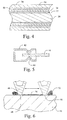
- FIG. 4 is a cross-sectional view of a conductive strip coated in accordance with a second embodiment of the invention.
- FIG. 5 is a cross-sectional view of the conductive strip of FIG. 4 subsequent to being formed into a connector assembly.
- FIG. 6 is a magnified cross-sectional view of a portion of the connector assembly of FIG. 5 illustrating the effect of fretting debris.
- FIG. 7 is a flow chart representation of a process to manufacture the first embodiment of the invention.
- FIG. 8 is a flow chart representation of a process to manufacture the second embodiment of the invention.
- FIG. 9 illustrates the interdiffusion between layers in coated substrates with different layer combinations.
- FIG. 10 is a photomicrograph of a surface of a coated substrate of the invention following heating to 150° C. for one week.
- FIG. 11 is a photomicrograph of a cross-section of the coated substrate of FIG. 10 .
- a leadframe has a plurality of leads 10 are formed from an electrically conductive metal, such as copper or a copper-base alloy. Each of the plurality of leads 10 terminates at an inner lead end 12 to define a central aperture that is occupied by a die paddle 14 .
- the inner lead ends 12 and die paddle 14 are coated with a thin layer of a precious metal, such as silver, to enhance chip attach and wire bonding.
- a precious metal such as silver
- One or more integrated circuit (IC) devices 16 are then attached to the die paddle 14 , such as through the use of a low temperature metallic solder or a thermally conductive polymer adhesive. Thin metal wires 18 , or thin strips of conductive metal foil, electrically interconnect circuits on an electrically active face of the integrated circuit device 16 to the inner lead ends 12 .
- a molding resin then encapsulates the die paddle 14 , integrated circuit device 16 , inner lead ends 12 and lead mid-portions 21 , generally along the perimeter identified by the broken line 20 .
- FIG. 2 is a side planar view of the assembly showing leads 10 extending from the molding resin 22 .
- Outer portions 23 of the leads extending from the molding resin are typically soldered to external circuitry, such as traces on a printed circuit board.
- the leads are typically formed from copper or a copper alloy, although non-copper leads such as iron-nickel and iron-nickel-cobalt alloys are used. Copper and copper alloys readily oxidize and the formation of an oxide on the surface. impedes soldering.
- a tarnish resistant layer on the copper leads.
- One readily solderable material for the anti-tarnish layer is tin or a tin-base alloy. When exposed to temperatures at or above room temperature, there is diffusion between the copper and the tin. As a copper-tin intermetallic forms on the surface of the layer, the anti-tarnish characteristics and solderability both degrade. It is known to dispose a barrier layer, such as nickel, between the anti-tarnish layer and the substrate to reduce the rate of diffusion and reduce the rate of intermetallic formation.
- Tin whiskering refers to a characteristic of tin where internal stresses are relieved by the growth of thin tin filaments. Referring back to FIG. 1 , the leads 10 are closely spaced and it is possible for a tin whisker to bridge the gap 24 between adjacent leads creating an electrical short circuit. Typically, a gap distance between leads of 1 millimeter or less is at risk of being bridged by a tin whisker. While numerous solutions for preventing tin whiskering have been proposed, these solutions have limitations. It is known reduce whiskering by alloying the tin with another metal, such as lead, but lead is toxic. It is known to heat the tin to above its melting temperature, a process known as reflow, to reduce whiskering. It is difficult to control the flow of molten tin and bridging between leads frequently results during reflow.
- tin whiskering is reduced by forming the lead 10 from a substrate 26 that is coated with a layer of silver or a silver-base alloy 28 , followed by a layer of fine grain tin 30 directly deposited on the layer of silver or silver-base alloy.
- directly deposited it is meant deposited to be adjoining, without any intervening layers of other materials.
- the substrate 26 is formed from a metal other than copper or a copper base alloy, a thin, on the order of 1-20 microinches layer of copper may be deposited on the substrate prior to deposition of the layer of silver 28 .
- the layer of silver 28 may be a silver-base alloy and the layer of tin may be a tin-base alloy.
- the interface between two metals tends to have less strength than the metal itself. Therefore, it is preferred that the portion of the leads 10 encapsulated by molding resin are not coated with the layers of silver and tin and these layers coat only those portions of the leads which extend outward from the molding resin,
- the layer of silver 28 has a thickness of between 1 microinch and 120 microinches. When the thickness is below 1 microinch, tin whiskering is not adequately suppressed. When the thickness is about 120 microinches, the cost becomes prohibitive.
- a preferred silver thickness is from 2 microinches to 40 microinches and a most preferred silver thickness is from 5 microinches to 20 microinches.
- the layer of tin 30 has a thickness of between 0.01 microinch and 400 microinches. When the tin thickness is less than 0.01 microinch, tarnish resistance and solderability are degraded. When the tin thickness exceeds 400 microinches, bridging between adjacent leads is likely.
- a preferred tin thickness is from 20 microinches to 150 microinches and a most preferred tin thickness is from 20 microinches to 80 microinches.
- the tin is fine grain, as achieved by electrodeposition, as opposed to coarser grain as achieved following reflow.
- the average grain size is from 0.1 micron to 100 microns, and preferably from 0.5 micron to 5 microns, as opposed to after reflow when the nominal grain size is on the order of millimeters.
- the fine grain structure has a generally higher ductility enabling the leads to be bent to a sharper radius without fracture of the coating layer. While a fine grain tin is believed more prone to whisker formation, the underlayer of silver enables use of fine grain tin in this embodiment.
- a second embodiment of the invention is drawn to connector assemblies. Unlike leadframes, most connector assemblies are not affected by tin whiskers since adjacent connectors are usually spaced apart far enough to avoid short circuiting by tin whiskers. Also, since connectors are not closely pitched like leads of a leadframe, reflow is available to reduce internal stresses in a tin coating. Further, diffusion between tin and copper is frequently desirable to reduce the thickness of free tin, thereby reducing friction and reducing the force needed to insert a probe into a socket.
- Connector assemblies are subject to an increase in resisitivy due to fretting debris.
- Fretting wear is a phenomenon that occurs between two surfaces having oscillatory relative motion of small amplitude. Fretting wear causes the removal of small particles from the contacting surfaces. These small particles subsequently oxidize and the oxidized debris accumulates at the interfaces of the connector assembly. Since the room temperature resistivity of tin is about 0.12 ⁇ m while the room temperature resistivity of tin oxide is about 1 ⁇ m, the result of fretting wear is a degrading of the connector assembly electrical properties.
- a substrate 26 is typically copper or a copper-base alloy, although other electrically conductive metals may be used. When one of those other electrically conductive metals is employed, a thin copper layer is deposited on the substrate as described above. The thin copper layer may also be deposited on a copper-base alloy substrate to provide a pure copper surface to facilitate deposition and adherence of subsequent layers.
- the barrier layer may be any metal that inhibits the diffusion of copper and the other constituents making up the substrate and is preferably a transition metal, such as nickel, cobalt, iron, manganese, chromium, molybdenum or their alloys.
- the barrier layer has a thickness of between 2 microinches and 80 microinches. If the barrier layer has a thickness of less than 2 microinches, it may not be effective to inhibit diffusion. If the barrier layer thickness exceeds 80 microinches, it may adversely affect the electrical and mechanical properties of the connector assembly.
- the thickness is between 4 microinches and 40 microinches. More preferably, the thickness of the barrier layer is between 4 microinches and 20 microinches.
- the sacrificial layer 34 is a metal that combines with both silver and tin to form alloys and intermetallic compounds. To reduce friction, the free tin thickness of outermost layer 36 is reduced. This thickness reduction may be accomplished by heating the assembly such that the sacrificial layer combines with the inner portion of the outermost layer to form relatively hard intermetallic compounds.
- a preferred material for the sacrificial layer is copper or a copper-base alloy having a thickness of between 2 microinches and 60 microinches.
- the thickness of the sacrificial layer is selected such that when the sacrificial layer is consumed, at least a thin, on the order of 2 microinches, layer of free tin preferably remains on the exterior surface 38 of the outermost layer 36 .
- a copper sacrificial layer has a most preferred thickness of between 5 and 20 microinches.
- a low resistivity oxide metal layer 40 Disposed between the sacrificial layer 34 and the outermost layer 36 is a low resistivity oxide metal layer 40 .
- This low resistivity oxide metal oxide is a metal that forms an oxide at the anticipated operating temperature of the connector assembly that has a resistivity which is less than the resistivity of tin oxide, Silver or a silver base alloy is preferred for the low resistivity oxide metal layer 40 .
- tin oxide has a room 30 temperature resistivity of about 1 ⁇ m
- silver oxide has a room temperature resistivity of about 0.14 ⁇ m.
- the thickness of the low resistivity oxide metal layer is between 2 microinches and 40 microinches and most preferably, between 5 microinches and 20 microinches.
- the conductive strip of FIG. 4 is formed into a connector assembly as shown in cross-sectional representation in FIG. 5 .
- the connector assembly includes a socket 42 and probe 44 .
- the socket is usually bent into a shape effective to make point contact with the probe with the shape also imparting an internal stress in the socket effective to apply a positive force to maintain electrical contact at the point 46 .
- FIG. 6 is a magnified view of the point contact identified by a broken circle in FIG. 5 . Due to vibration, the point 46 oscillates between a first contact point 48 and a second contact point 50 . This fretting generates fretting debris 52 in the form of metal oxides. A portion 54 of the fretting debris coats the oscillation track and impacts the flow of electric current between the point 46 and probe 44 .
- the low resistivity oxide metal layer is any metal that both forms an oxide with a resistivity less that of tin oxide (1 ⁇ m) or is a metal more noble than silver that has a low tendency to form oxides, such as gold, platinum and palladium.
- Table 1 identifies the oxides of many base metals and reports their suitability for use as the low resistivity oxide metal layer. In Table 1, “O” indicates suitability and “X” indicates not suitable.
- silver indium, iron, niobium, rhenium, ruthenium, vanadium, gold, platinum, palladium and zinc, as well as mixtures of these four metals are suitable.
- FIG. 7 is a flow chart representation of a method for the production of the coated substrate illustrated in FIG. 3 for use in applications where tin whiskering is a concern and tin reflow is not an option to relieve internal stress.
- Such applications include leadframes, closely spaced terminal pins (such as found in a pin grid array electronic package) and closely spaced circuit traces on a printed circuit board or flexible circuit.
- the first three process steps are specific to a leadframe and in some embodiments terminal pins. The remaining three steps are generic to all the above product lines.
- a leadframe is either stamped or chemically etched from a substrate, typically copper or a copper base alloy.
- the leadframe includes a centrally disposed die paddle and a plurality of leads extending outwardly from at least one, and typically all four sides of the die paddle.
- the leadframe is then degreased and cleaned, such as by a commercial degreaser, for an alkaline electrocleaner such as Hubbard-Hall E-9354 electrocleaner (available commercially from Hubbard-Hall, Waterbury, Conn.).
- An alkaline mixture along with anodic/cathodic electrocleaning allows generated oxygen or hydrogen bubbles to remove most impurities residing on the substrate.
- Electrocleaning is typically performed at about 20° C. to 55° C. for about one minute with a current density range of about 10 to 50 asf (amps per square foot).
- the die paddle and inner portions of the leads are then coated 56 with a metal that enhances solderability and wire bonding, such as silver to a thickness of from 3 microns to 6 microns. It is preferable that only the innermost portion of the leads, the part utilized for wire bonding or tape automated bonding (TAB) be silver coated. This is because during the subsequent encapsulation step 58 , it is desired for the molding resin to directly contact the copper substrate, providing a single interface for adhesion failure and moisture egress. Less preferred is a two interface arrangement where the molding resin contacts the silver layer that contacts the copper substrate.
- the silver coating 56 may be by any suitable process, such as electrodeposition, electroless deposition, immersion coating, chemical vapor deposition or plasma deposition.
- the IC device is then bonded to the die paddle by convention die attach methods 60 such as soldering with a low temperature solder, for example a gold/tin eutectic, or adhesive joining, such as with a metal filled epoxy.
- Wire bonding employs small diameter wires or thin strips of metal foil to electrically interconnect the IC device to the inner lead portions of the leadframe.
- the die paddle, IC device, wire bonds and inner lead portions of the leadframe are encapsulated in a thermosetting molding resin, such as an epoxy.
- the outer portions of the leads are then bent into a desired shape for bonding to a printed circuit board or other external circuit.
- the outer lead portions are then coated 62 with a layer of silver or silver alloy, by any suitable process, such as electroplating, electroless plating, immersion plating, physical vapor deposition, chemical vapor deposition, plasma deposition or metal spraying.
- the silver is applied to a thickness of from 1 microinch to 120 microinches, with a thickness of from 2 microinches to 20 microinches being most preferred.
- a preferred method of depositing the layer of silver is by electroplating from an aqueous solution containing 31-56 grams per liter silver cyanide, 50-78 g/l potassium cyanide, 15-90 g/l potassium carbonate and brighteners. Electroplating is at a temperature of between 20° and 28° C. at a current density of between 5 amps per square foot and 15 asft Alternatively, the silver layer can be deposited using cyanide-free immersion plating such as MacDermid SterlingTM silver (MacDermid Inc., Waterbury, Conn.).
- a layer of tin is then coated 64 on the Ag coated outer leads to a thickness of from 0.006 microinch to 400 microinches and preferably to a thickness of from 20 microinches to 80 microinches,
- a preferred method of depositing the layer of tin is by electroplating from a solution containing methane sulfonic acid based tin plating solution such as Rohm and Haas SolderonTM ST200 (Rohm and Haas Company, Philadelphia, Pa.) or MacDermid StanTekTM AMAT for matte tin. MacDermid StanTekTM Stellite is useful for bright tin.
- Typical operating conditions for the above electrolytes are a temperature of 25° C.-35° C. and a current density of between 5 asf and 50 asf.
- the tin coated exterior leads are then bonded 66 to a printed circuit board or other external circuit, such as by soldering using either a tin/lead alloy solder or appropriate leadfree solder.
- solder and soldering process are selected to enable the solder to fuse to the layer of tin without the layer of tin melting. Melting of the layer of tin is to be avoided to prevent bridging of liquid solder between leads.
- FIG. 8 is a flow chart representation of a method for the production of the coated substrate illustrated in FIG. 4 for use in applications where the effect of the oxidized debris of fretting wear on electrical resistivity is a concern, such as in electrical connector assemblies.
- the substrate is not copper, or where the substrate is a copper alloy having a high (for example greater than 2%, by weight) alloy content, it is desirable to deposit 68 a thin copper layer on the surfaces of the substrate prior to deposition of subsequent layers.
- the thin copper layer minimizes the effect of different metals on the deposition of subsequent layers leading to more consistent product performance for many different substrate materials.
- the copper layer has a minimum thickness of 5 microinches and has a typical thickness of between 20 microinches and 40 microinches. While the copper layer and the subsequent layers described below may be deposited by any suitable method, a preferred method of depositing 68 the layer of copper is by electroplating from an aqueous solution containing from 20 g/l to 70 g/l of copper ions and from 50 g/l to 200 g/l of sulfuric acid. Operating conditions are a temperature of from 40° C. to 60° C. at a current density of from 20 asf to 100 asf.
- a barrier layer is next deposited 70 .
- Suitable barrier layers include nickel, cobalt, chromium, molybdenum, iron and manganese and their alloys or mixtures deposited to a thickness of from 2 microinches to 40 microinches and preferably to a thickness of from 4 microinches to 20 microinches.
- a preferred method of depositing 70 the layer of nickel is by electroplating from an aqueous solution nominally containing 300 g/l of nickel sulfamate, 6 g/l of nickel chloride and 30 g/l of boric acid. Operating conditions are a temperature of from 28° C. to 60° C., a pH of from 3.5 to 4.2 and a current density of from 2 asf to 30 asf.
- the layer of free tin should be on the order of 2 microinches to 120 microinches to provide a solderable, tarnish resistant, layer.
- the intermetallic layer is useful to reduce friction by reducing the thickness of soft free tin. Reduced friction leads to reduced insertion force required for the connector assembly.
- a metal that forms a low resistivity oxide such as silver
- the sacrificial layer is deposited to a thickness of from 1 microinch to 120 microinches and preferably to a thickness of from 5 microinches to 20 microinches.
- a preferred method of depositing the sacrificial layer of silver is by electroplating from an aqueous solution containing silver cyanide or by immersion plating from a cyanide-free solution as described above.
- indium, iron, niobium, rhenium, ruthenium, vanadium, gold, platinum, palladium and zinc, as well as mixtures of these metals may be employed as illustrated above in Table 1.
- an outermost layer of a metal having a melting temperature less than the melting temperature of any one of the substrate, the barrier layer, the sacrificial layer and the low resistivity oxide metal layer is deposited 76 .
- Tin or tin-base alloys are preferred for the outermost layer, For most applications, lead is avoided for toxicity concerns; however, a tin-base alloy containing lead may be suitable for some applications.
- the outermost layer is deposited 76 by any of the methods described above or by tin deposition specific methods such as HALT (hot air level tin) process and mechanical wipe.
- the outermost layer can have a bright or matte finish, as desired.
- a matte finish may be produced by electroplating tin from a tin bath that is known in the art for preparing this type of finish. Suitable electrolytes include SolderonTM ST200 and StanTekTM AMAT as described above.
- the tin is then reflowed 78 , such as by heating to a temperature above the melting point of tin (232° C.) to reflow the tin.
- a preferred thermal profile is 300° C. for a few (1-10) seconds in air or in a protective atmosphere, such as nitrogen.
- the molten tin is then quenched to produce a lustrous appearance.
- the coated substrate is formed 80 into a desired component, such as part of a connector assembly.
- the coated substrate may also be heated in air or nitrogen at a temperature less than the melting temperature of the tin to increase the amount of intermetallic and reduce the free tin to a desired thickness, typically from 2 microinches to 20 microinches. This heating may be at a temperature of from 150° C. to 200° C. for from 1 hour to 168 hours.
- FIG. 9A illustrates a tin coated substrate 26 as known form the prior art.
- the substrate 26 is coated with a sacrificial layer of copper 34 and an outermost tin layer 36 .
- elevated temperatures such as 150° C. for one week
- interdiffusion and combining occur between the sacrificial layer 34 and outermost layer 36 to form a Cu 3 Sn intermetallic layer 82 adjacent the substrate 26 that extends upwards to the surface 84 of the outermost layer.
- the outermost layer after elevated temperature exposure is a mixture of the Cu 3 Sn intermetallic and the Cu 6 Sn 5 intermetallic 86 .
- FIG. 9B illustrates that, in accordance with the invention, when the substrate 26 is coated with a sacrificial layer 34 , silver layer 28 and outermost tin coating layer 36 and then heated to 150° C. for one week, the substrate 26 is coated with an intervening layer 88 that is a mixture of copper and tin while the outermost layer is a mixture of silver containing Cu 3 Sn intermetallic 90 and a silver-rich phase 92 .
- silver-rich it is meant that the phase contains in excess of 50 atomic % silver.
- the Cu 3 SnAg x intermetallic provides a hard surface to reduce insertion force and reduce fretting wear.
- the silver-rich phase provides tarnish resistance and reduces the increase in resistivity due to fretting wear debris corrosion.
- FIG. 9C illustrates that, in accordance with the invention, when the substrate 26 is coated with a barrier layer 32 , sacrificial layer 34 , silver layer 28 and outermost tin coating 36 and then heated to 150° C. for one week, the substrate 26 is then coated with intervening layer 96 that is a mixture of nickel, copper and tin. Adjacent the layer 96 is a second layer 98 that is a mixture of nickel, copper, silver and tin. The outermost layer is a mixture a first component which is Cu 6 Sn 5 intermetallic and excess tin and a trace of silver and a second component which is the silver-rich phase 92 .
- FIG. 10 is a photomicrograph, at a magnification of 2000 times, of the outermost surface 84 of the coated substrate of FIG. 9C after heating to 150° C. for one week.
- the surface is a mixture of copper-silver-tin phase 98 , which appears as dark regions in the photomicrograph, and silver-rich phase 92 , which appears as light regions in the photomicrograph.
- FIG. 11 is a photomicrograph, at a magnification of 20,000 times, of the coated structure of FIGS. 9C and 10 .
- FIG. 9D illustrates that when the substrate 26 is coated with a barrier layer 32 , silver layer 28 and outermost coating layer of tin 36 and then heated to 150° C. for one week, the substrate 26 is then coated with a first intervening layer 100 that is a mixture of nickel, copper and tin with a trace of silver.
- the first intervening layer 100 is coated with a second layer 102 that is a mixture of copper, nickel, tin and silver. This second layer 102 extends to the surface of the outermost layer which is predominantly the silver-rich phase 92 .
- Coupons 2 inches ⁇ 0.5 inch ⁇ 0.010 inch thick were cut from a strip of copper alloy C194.
- Copper alloy C194 has a composition by weight of 2.1%-2.6% iron, 0.05%-0.20% zinc, 0.015%-0.15% phosphorous and the balance is copper.
- the coupons were cleaned in a commercial alkaline cleaner at 50° C. using a cathodic current density of 15 asf (amps per square foot) for 1 minute.
- the Ni plating solution was an aqueous solution containing from about 60 to 75 g/l (grams per liter) Ni as Ni sulfamate, about 6 to 8 g/l NiCl 2 , and about 38 to 53 g/l boric acid at 53° C. with a pH between about 3.5 and 4.2.
- the Ni plating conditions were 30 asf for about 60 seconds.
- deposition was by electroplating from an aqueous solution containing about 20 to 70 g/l Cu and about 50 to 200 g/l H 2 SO 4 at 40-60° C. using a current density of 40 asf for about 40 sec.
- deposition was made in an aqueous solution containing 31-56 g/l silver cyanide, 50-78 g/l potassium cyanide, 15-90 g/l potassium carbonate and brighteners. Operating conditions were a temperature of from 20° C. to 28° C. and a current density of from 5 asf to 15 asf.
- Tin was deposited by electroplating from the MacDermid StanTekTM AMAT solution for matte tin deposits and from the MacDermid StanTekTM Stellite 100 solution for bright tin deposits.
- the plating conditions were 30 asf for about 50 to 400 seconds at 25° C. to 40° C.
- Coupons having the dimensions 6 inches by 1.25 inches by 0.005 inch were formed from copper alloys C194 and C7025, wrought monolithic tin and wrought monolithic silver as noted in Table 3.
- C7025 has a composition, by weight, of 2.2%-4.2% nickel, 0.25%-1.2% silicon, 0.05%-0.3% Mg and the balance is copper.
- the copper alloy coupons were coated with intervening layers and matte tin as in Example 1 except that the silver layer was deposited by the immersion method using MacDermid SterlingTM silver solution and the tin was deposited from a sulfate solution containing 20 g/l to 80 g/l of tin ions as SnSO 4 50 g/l to 200 g/l sulfuric acid, and organic additives.
- fretting wear on contact resistance was determined by moving a 1 ⁇ 4′′ diameter bump at 5 Hz up to 20,000 cycles with a cycle length of 20 ⁇ m across a contact surface to be tested. A normal force of 100g was applied to the bump, and contact resistance data was collected while the bump was in motion. The values reported are the number of cycles required to achieve a specified contact resistance, A higher number of cycles indicates a better resistance to fretting.
- Comparing Sample 2 of the invention to Sample 1 demonstrates that the addition of a 5 ⁇ in silver layer was effective to reduce the fretting wear induced resistance of the substrate by about a 30% increase in the number of cycles needed to reach 10 m ⁇ contact resistance and about a 35% increase in the number of cycles needed to reach 10 ⁇ contact resistance.
- Comparing Sample 4 of the invention to Sample 3 demonstrates that the addition of a 5 ⁇ in silver layer was effective to reduce the fretting wear induced resistance of the substrate by about a 322% increase in the number of cycles needed to reach 10 m ⁇ contact resistance and in excess of a 120% increase in the number of cycles needed to reach 10 ⁇ contact resistance.
- Monolithic wrought Ag (Sample 6) had better performance than any of the samples having a coated copper substrate, but is not practical to form an electrical connector due to cost and tarnish.
- Monolithic wrought Sn (Sample 5) had a reasonably good fretting-resistant probably due to the abundance of free Sn or increased hardness resulting from rolling, but is not practical as a connector due to a lack of strength.
- Copper alloy C194 coupons having the dimensions 6 inch ⁇ 1.25 inch ⁇ 0.005 inch were coated with intervening layers and matte tin as in the preceding examples.
- a reflowed tin surface was obtained by heating a sample to 350° C. in air and quenching in water.
- the coefficient of friction was measured as the ratio of the resistive force relative to the normal force (R/N) when a 1 ⁇ 4 inch diameter bump slid at 3 mm/sec for 10 cycles across a tin coated flat surface.
- the normal force was loaded as dead weight and no lubricant was applied between the tin coated surface and the bump.
- the resistive force was measured as the bump was slid against the flat surface of the sample. The value reported was the average of all 10 cycles. A lower R/N indicates less friction.
- Tables 5 through 8 report the measured compositions of the structures illustrated in FIGS. 9A though 9 D to demonstrate the formation of a silver-rich phase on the outermost surface of substrates coated in accordance with the invention.
- EDX analysis results may vary by a few percent due to x-ray beam spread and depth of penetration. However, for comparison purpose, the above results are useful to differentiate among samples.
Abstract
Description
| TABLE 1 | |||||
| Room | |||||
| Temperature | |||||
| Resistivity | |||||
| Base Metal | Oxide | (Ω · m) | Suitability | ||
| Resistivity | Cadmium | CdO | 3.90E−05 | X - Toxic |
| Acceptable | Indium | In2O3 | 1.00E−03 | ◯ |
| Iron | Fe3O4 | 1.00E−04 | ◯ | |
| Niobium | Nb2O3 | 8.60E−04 | ◯ | |
| Rhenium | ReO3 | 2.00E−05 | ◯ | |
| Ruthenium | Ru2O | 3.52E−07 | ◯ | |
| Silver | AgO | 0.14 | ◯ | |
| Uranium | UO2 | 3.80E−02 | X - Toxic | |
| Vanadium | V2O3 | 5.50E−05 | ◯ | |
| Zinc | ZnO | 1.50E−02 | ◯ | |
| Resistivity | Bismuth | Bi2O3 | 1.00E+07 | |
| Not | Cobalt | CoO | 1.00E+06 | |
| Acceptable | Copper | Cu2O | 2.00E+05 | |
| Europium | EuO | 1.00E+06 | ||
| Manganese | MnO | 1.00E+06 | ||
| Nickel | NiO | 1.00E+11 | ||
| Silicon | SiO2 | 1.00E+12 | ||
| Sodium | Na202 | 2.50E+02 | ||
| Tantalum | Ta2O5 | 1.00E+03 | ||
| TABLE 2 | ||||
| Intervening | Number of whiskers | |||
| Layers, | per mm2 and length of | |||
| Thickness in | Tin | longest whisker in microns | ||
| Tin | microinches | thick. in | 10 days | 60 days | 120 days | 180 days |
| Sample | Finish | Ni | Cu | Ag | μinches | # | μm | # | μm | # | μm | # | μm |
| 1 | matte | -0- | 20-40 | -0- | 250-500 | 25 | 19 | 58 | 28 | 138 | 36 | 295 | 53 |
| 2 | matte | -0- | 20-40 | -0- | 75-130 | 33 | 28 | 298 | 175 | 310 | 87 | 496 | 169 |
| 3 | matte | -0- | 20-40 | 5-10 | 75-130 | -0- | -0- | -0- | -0- | -0- | -0- | -0- | -0- |
| 4 | matte | -0- | 20-40 | -0- | 40-80 | 108 | 36 | 389 | 45 | 361 | 130 | 512 | 45 |
| 5 | matte | -0- | 20-40 | 5-10 | 40-80 | -0- | -0- | -0- | -0- | -0- | -0- | 5 | 5 |
| 17 | matte | 5-20 | -0- | 5-10 | 40-80 | -0- | -0- | -0- | -0- | -0- | -0- | 2 | 4 |
| 19 | matte | 5-20 | 7-18 | 5-10 | 40-80 | -0- | -0- | -0- | -0- | -0- | -0- | -0- | -0- |
| 20 | bright | -0- | 20-40 | -0- | 40-80 | 8 | 7 | 33 | 7 | 30 | 9 | 231 | 28 |
| 21 | bright | -0- | 20-40 | 5-10 | 40-80 | -0- | -0- | -0- | -0- | -0- | -0- | -0- | -0- |
| TABLE 3 | ||||||
| Surface | Cycles to | Cycles to | ||||
| Layer | 10 mΩ | 10 Ω | ||||
| Intervening | Surface | Thickness | Contact | Contact | ||
| Sample | Substrate | Layers | Layer | (μinch) | Resistance | Resistance |
| 1 | C194 | Ni/ | Matte Tin | 20 | 61 | 3269 | |
| 2 | C194 | Ni/Cu/5 μinch | Matte Tin | 20 | 79 | 4400 | |
| 3 | C194 | | Matte Tin | 40 | 116 | 2269 | |
| 4 | C194 | 5 μinch | Matte Tin | 42 | 490 | >5000* | |
| 5 | Wrought | None | None | N/A | 253 | 6530 | |
| Tin | |||||||
| 6 | Wrought | None | None | N/A | >20,000 | >20,000 | |
| Ag | |||||||
| *Testing terminated after 5000 cycles | |||||||
| TABLE 4 | |||||
| Intervening | |||||
| Layers - | |||||
| Thickness in | Tin | R/N | |||
| μinch | Thickness | 0-60 mm | |||
| Sample | Cu | Ag | Tin Type | μinch | 100 g | 250 g |
| 1 | 20-40 | -0- | Matte | 40-80 | 0.55 | 0.55 |
| 2 | 20-40 | 2-5 | Matte | 40-80 | 0.58 | 0.53 |
| 3 | 20-40 | 5-10 | Matte | 40-80 | 0.48 | 0.45 |
| 4 | 20-40 | 10-20 | Matte | 40-80 | 0.47 | 0.46 |
| 5 | -0- | -0- | |
40 | 0.48 | 0.47 |
| 6 | -0- | 5 | |
40 | 0.30 | 0.22 |
| TABLE 5 |
| (FIG. 9A) |
| Ref. No. | Ref. No. | |||||
| from FIG. | Thickness | from FIG. | Atomic | |||
| 9A | Composition | (μinches) | | Composition | Percent | |
| 26 | C194 | N.A. | 26 | C194 | N.A. | |
| 34 | Copper | 20-40 | 82 | Copper | 75% | |
| Tin | 25% | |||||
| 36 | Tin | 40-80 | 86 | |
56 | |
| Tin | ||||||
| 44% | ||||||
| TABLE 6 |
| (FIG. 9B) |
| Ref. No. | Ref. No. | |||||
| from FIG. | Thickness | from FIG. | Atomic | |||
| 9B | Composition | (μinches) | | Composition | Percent | |
| 26 | C194 | N.A. | 26 | C194 | N.A. | |
| 34 | Copper | 20-40 | 88 | Copper | 79 | |
| Tin | ||||||
| 21% | ||||||
| 28 | Silver | 5-10 | 90 | |
74 | |
| Tin | ||||||
| 23% | ||||||
| Silver | 3% | |||||
| 36 | Tin | 40-89 | 92 | |
56% | |
| Tin | 25% | |||||
| Copper | 19% | |||||
| TABLE 7 |
| (FIG. 9C) |
| Ref. No. | Ref. No. | |||||
| from FIG. | Thickness | from FIG. | Atomic | |||
| 9C | Composition | (μinches) | | Composition | Percent | |
| 26 | C194 | N.A. | 26 | C194 | N.A. | |
| 32 | Nickel | 5-20 | 96 | |
42 | |
| Nickel | ||||||
| 32 | ||||||
| Tin | ||||||
| 26% | ||||||
| 34 | Copper | 7-18 | 98 | |
50% | |
| Tin | 41% | |||||
| Nickel | 7% | |||||
| Silver | 2% | |||||
| 28 | Silver | 5-10 | 94 | Tin | 77% | |
| Copper | 17% | |||||
| Silver | 6% | |||||
| 36 | Tin | 40-80 | 92 | |
56% | |
| Tin | 31% | |||||
| Copper | 13% | |||||
| TABLE 8 |
| (FIG. 9D) |
| Ref. No. | Ref. No. | |||||
| from FIG. | Thickness | from FIG. | Atomic | |||
| 9D | Composition | (μinches) | | Composition | Percent | |
| 26 | C194 | N.A. | 26 | C194 | N.A. |
| 32 | Nickel | 5-20 | 100 | Tin | 41 |
| Nickel | |||||
| 34 | |||||
| Copper | |||||
| 24% | |||||
| Silver | 1% | ||||
| 28 | Silver | 5-10 | 102 | Tin | 35% |
| Silver | 27 | ||||
| Copper | |||||
| 23% | |||||
| Nickel | 15% | ||||
| 36 | Tin | 40-80 | 92 | |
64 |
| Tin | |||||
| 26 | |||||
| Copper | |||||
| 10% | |||||
Claims (25)
Priority Applications (1)
| Application Number | Priority Date | Filing Date | Title |
|---|---|---|---|
| US12/145,420 US7808109B2 (en) | 2003-10-14 | 2008-06-24 | Fretting and whisker resistant coating system and method |
Applications Claiming Priority (3)
| Application Number | Priority Date | Filing Date | Title |
|---|---|---|---|
| US51124903P | 2003-10-14 | 2003-10-14 | |
| US10/962,917 US7391116B2 (en) | 2003-10-14 | 2004-10-12 | Fretting and whisker resistant coating system and method |
| US12/145,420 US7808109B2 (en) | 2003-10-14 | 2008-06-24 | Fretting and whisker resistant coating system and method |
Related Parent Applications (1)
| Application Number | Title | Priority Date | Filing Date |
|---|---|---|---|
| US10/962,917 Continuation US7391116B2 (en) | 2003-10-14 | 2004-10-12 | Fretting and whisker resistant coating system and method |
Publications (2)
| Publication Number | Publication Date |
|---|---|
| US20090017327A1 US20090017327A1 (en) | 2009-01-15 |
| US7808109B2 true US7808109B2 (en) | 2010-10-05 |
Family
ID=34465205
Family Applications (2)
| Application Number | Title | Priority Date | Filing Date |
|---|---|---|---|
| US10/962,917 Active 2025-06-16 US7391116B2 (en) | 2003-10-14 | 2004-10-12 | Fretting and whisker resistant coating system and method |
| US12/145,420 Active US7808109B2 (en) | 2003-10-14 | 2008-06-24 | Fretting and whisker resistant coating system and method |
Family Applications Before (1)
| Application Number | Title | Priority Date | Filing Date |
|---|---|---|---|
| US10/962,917 Active 2025-06-16 US7391116B2 (en) | 2003-10-14 | 2004-10-12 | Fretting and whisker resistant coating system and method |
Country Status (8)
| Country | Link |
|---|---|
| US (2) | US7391116B2 (en) |
| JP (4) | JP4708357B2 (en) |
| KR (2) | KR101351284B1 (en) |
| CN (2) | CN100594604C (en) |
| HK (1) | HK1118950A1 (en) |
| MY (1) | MY144068A (en) |
| TW (1) | TWI258826B (en) |
| WO (1) | WO2005038989A2 (en) |
Cited By (8)
| Publication number | Priority date | Publication date | Assignee | Title |
|---|---|---|---|---|
| US20110038135A1 (en) * | 2008-04-29 | 2011-02-17 | Iljin Copper Foil Co., Ltd. | Metal frame for electronic part |
| US20140342113A1 (en) * | 2013-04-11 | 2014-11-20 | United States Of America As Represented By The Secretary Of The Navy | Structures and methods related to detection, sensing, and/or mitigating undesirable structures or intrusion events on structures |
| US20150011132A1 (en) * | 2012-02-03 | 2015-01-08 | Jx Nippon Mining & Metals Corporation | Press-fit terminal and electronic component using the same |
| US20160285186A1 (en) * | 2013-03-21 | 2016-09-29 | Enplas Corporation | Electrical connector and socket for electrical component |
| US9576693B2 (en) | 2011-09-20 | 2017-02-21 | Jx Nippon Mining & Metals Corporation | Metal material for electronic component and method for manufacturing the same |
| US9580783B2 (en) | 2011-10-04 | 2017-02-28 | Jx Nippon Mining & Metals Corporation | Electronic component metal material and method for manufacturing the same |
| US10530084B2 (en) | 2012-06-27 | 2020-01-07 | Jx Nippon Mining & Metals Corporation | Metallic material for electronic components and method for producing same, and connector terminals, connectors and electronic components using same |
| US10594066B2 (en) | 2012-06-27 | 2020-03-17 | Jx Nippon Mining & Metals Corporation | Metallic material for electronic components and method for producing same, and connector terminals, connectors and electronic components using same |
Families Citing this family (73)
| Publication number | Priority date | Publication date | Assignee | Title |
|---|---|---|---|---|
| JP4758614B2 (en) * | 2003-04-07 | 2011-08-31 | ローム・アンド・ハース・エレクトロニック・マテリアルズ,エル.エル.シー. | Electroplating composition and method |
| US20060091121A1 (en) * | 2004-10-06 | 2006-05-04 | James Zanolli | Method for reflowing a metal plating layer of a contact and contact formed thereby |
| US20060266446A1 (en) * | 2005-05-25 | 2006-11-30 | Osenbach John W | Whisker-free electronic structures |
| JP2007081235A (en) * | 2005-09-15 | 2007-03-29 | Renesas Technology Corp | Method of manufacturing semiconductor device |
| JP4817095B2 (en) * | 2005-10-03 | 2011-11-16 | 上村工業株式会社 | Whisker suppression surface treatment method |
| JP4868892B2 (en) * | 2006-03-02 | 2012-02-01 | 富士通株式会社 | Plating method |
| US20070284700A1 (en) * | 2006-06-07 | 2007-12-13 | Honeywell International, Inc. | Coatings and methods for inhibiting tin whisker growth |
| US20070287023A1 (en) * | 2006-06-07 | 2007-12-13 | Honeywell International, Inc. | Multi-phase coatings for inhibiting tin whisker growth and methods of making and using the same |
| US20070287022A1 (en) * | 2006-06-07 | 2007-12-13 | Honeywell International, Inc. | Intumescent paint coatings for inhibiting tin whisker growth and methods of making and using the same |
| US20070295530A1 (en) * | 2006-06-07 | 2007-12-27 | Honeywell International, Inc. | Coatings and methods for inhibiting tin whisker growth |
| US10873002B2 (en) * | 2006-10-20 | 2020-12-22 | Cree, Inc. | Permanent wafer bonding using metal alloy preform discs |
| EP2089901A4 (en) | 2006-11-09 | 2011-05-18 | Interplex Qlp Inc | Microcircuit package having ductile layer |
| US10231344B2 (en) | 2007-05-18 | 2019-03-12 | Applied Nanotech Holdings, Inc. | Metallic ink |
| US8404160B2 (en) * | 2007-05-18 | 2013-03-26 | Applied Nanotech Holdings, Inc. | Metallic ink |
| US20080308300A1 (en) * | 2007-06-18 | 2008-12-18 | Conti Mark A | Method of manufacturing electrically conductive strips |
| JP5001731B2 (en) * | 2007-07-02 | 2012-08-15 | 日東電工株式会社 | Connection structure between printed circuit board and electronic components |
| JP5215305B2 (en) * | 2007-07-06 | 2013-06-19 | 第一電子工業株式会社 | Electronic component manufacturing method and electronic component manufactured by the method |
| WO2009017870A1 (en) * | 2007-07-31 | 2009-02-05 | Textron Systems Corporation | Techniques for direct encasement of circuit board structures |
| JP4942580B2 (en) * | 2007-08-20 | 2012-05-30 | 株式会社荏原製作所 | Current carrying belt for anode holder and anode holder |
| DE102007047007A1 (en) * | 2007-10-01 | 2009-04-09 | Tyco Electronics Amp Gmbh | Electrical contact element and a method for producing the same |
| US8506849B2 (en) | 2008-03-05 | 2013-08-13 | Applied Nanotech Holdings, Inc. | Additives and modifiers for solvent- and water-based metallic conductive inks |
| US9730333B2 (en) * | 2008-05-15 | 2017-08-08 | Applied Nanotech Holdings, Inc. | Photo-curing process for metallic inks |
| US20090286383A1 (en) * | 2008-05-15 | 2009-11-19 | Applied Nanotech Holdings, Inc. | Treatment of whiskers |
| WO2009140524A2 (en) * | 2008-05-15 | 2009-11-19 | Interplex Industries, Inc. | Tin-silver compound coating on printed circuit boards |
| US20100000762A1 (en) * | 2008-07-02 | 2010-01-07 | Applied Nanotech Holdings, Inc. | Metallic pastes and inks |
| US20110162707A1 (en) * | 2008-07-07 | 2011-07-07 | Sandvik Intellectual Property Ab | Electrical contact with anti tarnish oxide coating |
| JP5384382B2 (en) * | 2009-03-26 | 2014-01-08 | 株式会社神戸製鋼所 | Copper or copper alloy with Sn plating excellent in heat resistance and method for producing the same |
| TWI492303B (en) | 2009-03-27 | 2015-07-11 | Applied Nanotech Holdings Inc | Buffer layer to enhance photo and/or laser sintering |
| US8652649B2 (en) * | 2009-07-10 | 2014-02-18 | Xtalic Corporation | Coated articles and methods |
| JP5612355B2 (en) * | 2009-07-15 | 2014-10-22 | 株式会社Kanzacc | Plating structure and method of manufacturing electrical material |
| US8422197B2 (en) * | 2009-07-15 | 2013-04-16 | Applied Nanotech Holdings, Inc. | Applying optical energy to nanoparticles to produce a specified nanostructure |
| JP5442385B2 (en) * | 2009-10-07 | 2014-03-12 | 三菱伸銅株式会社 | Conductive member and manufacturing method thereof |
| WO2011151770A1 (en) * | 2010-06-01 | 2011-12-08 | Koninklijke Philips Electronics N.V. | Kit of parts, contacting element and luminaire |
| US20120090880A1 (en) | 2010-10-19 | 2012-04-19 | International Business Machines Corporation | Mitigation and elimination of tin whiskers |
| JP2012107263A (en) * | 2010-11-15 | 2012-06-07 | Kyowa Densen Kk | Plating structure and coating method |
| JP6204348B2 (en) | 2011-05-04 | 2017-09-27 | リキッド エクス プリンテッド メタルズ インコーポレイテッド | Metal alloy derived from molecular ink |
| WO2012178052A1 (en) * | 2011-06-23 | 2012-12-27 | Xtalic Corporation | Printed circuit boards and related articles including electrodeposited coatings |
| DE102011078546A1 (en) | 2011-07-01 | 2013-01-03 | Tyco Electronics Amp Gmbh | Electrical contact coating |
| JP6046406B2 (en) * | 2011-07-26 | 2016-12-14 | ローム アンド ハース エレクトロニック マテリアルズ エルエルシーRohm and Haas Electronic Materials LLC | High temperature resistant silver coated substrate |
| JP5138827B1 (en) * | 2012-03-23 | 2013-02-06 | Jx日鉱日石金属株式会社 | Metal materials for electronic parts, connector terminals, connectors and electronic parts using the same |
| DE102012208681A1 (en) * | 2012-05-24 | 2013-11-28 | Robert Bosch Gmbh | Tin coating, associated contact element and method for applying a tin coating |
| JP5427945B2 (en) * | 2012-06-27 | 2014-02-26 | Jx日鉱日石金属株式会社 | METAL MATERIAL FOR ELECTRONIC COMPONENT AND ITS MANUFACTURING METHOD, CONNECTOR TERMINAL USING THE SAME, CONNECTOR AND ELECTRONIC COMPONENT |
| WO2014011578A1 (en) | 2012-07-09 | 2014-01-16 | Applied Nanotech Holdings, Inc. | Photosintering of micron-sized copper particles |
| TWI465333B (en) | 2012-07-25 | 2014-12-21 | Jx Nippon Mining & Metals Corp | Electronic material for electronic parts and method for manufacturing the same, use of its connector terminals, connectors and electronic parts |
| TWI488733B (en) * | 2012-10-04 | 2015-06-21 | Jx Nippon Mining & Metals Corp | Metal material for electronic parts and manufacturing method thereof |
| TWI485930B (en) * | 2012-10-04 | 2015-05-21 | Jx Nippon Mining & Metals Corp | Metal material for electronic parts and manufacturing method thereof |
| US9755059B2 (en) | 2013-06-09 | 2017-09-05 | Cree, Inc. | Cascode structures with GaN cap layers |
| US9847411B2 (en) | 2013-06-09 | 2017-12-19 | Cree, Inc. | Recessed field plate transistor structures |
| US10351965B2 (en) * | 2013-06-24 | 2019-07-16 | Oriental Electro Plating Corporation | Method for producing plated material, and plated material |
| US10260159B2 (en) | 2013-07-05 | 2019-04-16 | The Boeing Company | Methods and apparatuses for mitigating tin whisker growth on tin and tin-plated surfaces by doping tin with gold |
| US10633754B2 (en) | 2013-07-05 | 2020-04-28 | The Boeing Company | Methods and apparatuses for mitigating tin whisker growth on tin and tin-plated surfaces by doping tin with germanium |
| CN103498044A (en) * | 2013-09-26 | 2014-01-08 | 苏州米达思精密电子有限公司 | Coiled strip metal raw material sand blasting deformation stress relief device |
| JP2015067861A (en) * | 2013-09-30 | 2015-04-13 | 株式会社オートネットワーク技術研究所 | Electrical contact material for connector and production method thereof |
| WO2015092979A1 (en) * | 2013-12-20 | 2015-06-25 | オリエンタル鍍金株式会社 | Silver-plated member, and production method therefor |
| JP6665387B2 (en) * | 2013-12-20 | 2020-03-13 | オリエンタル鍍金株式会社 | Silver plated member and method of manufacturing the same |
| JP6374718B2 (en) * | 2014-07-14 | 2018-08-15 | 矢崎総業株式会社 | Electrical element |
| DE102014117410B4 (en) * | 2014-11-27 | 2019-01-03 | Heraeus Deutschland GmbH & Co. KG | Electrical contact element, press-fit pin, socket and leadframe |
| DE102015102453A1 (en) * | 2015-02-20 | 2016-08-25 | Heraeus Deutschland GmbH & Co. KG | Ribbon-shaped substrate for the production of chip card modules, chip card module, electronic device with such a chip card module and method for producing a substrate |
| TWI542729B (en) * | 2015-07-09 | 2016-07-21 | 旭德科技股份有限公司 | Circuit board and manufacturing method thereof |
| JP6558533B2 (en) * | 2015-07-31 | 2019-08-14 | 住電機器システム株式会社 | Connecting member |
| CN105420534A (en) * | 2015-11-06 | 2016-03-23 | 广西南宁智翠科技咨询有限公司 | Alloy conducting wire with ultrahigh electric conductivity |
| KR102355341B1 (en) * | 2016-05-10 | 2022-01-24 | 미쓰비시 마테리알 가부시키가이샤 | Tinned copper terminal material and terminal and wire termination structures |
| KR101900793B1 (en) | 2017-06-08 | 2018-09-20 | 주식회사 풍산 | A method for tin plating copper alloy for electrical and electronic and car components, and tin plated copper alloy therefrom |
| EP3705608A4 (en) * | 2017-11-01 | 2021-08-11 | Nippon Steel Corporation | Electrolytically sn-plated steel sheet |
| CN110265376A (en) | 2018-03-12 | 2019-09-20 | 意法半导体股份有限公司 | Lead frame surface finishing |
| US10453817B1 (en) | 2018-06-18 | 2019-10-22 | Texas Instruments Incorporated | Zinc-cobalt barrier for interface in solder bond applications |
| US11735512B2 (en) * | 2018-12-31 | 2023-08-22 | Stmicroelectronics International N.V. | Leadframe with a metal oxide coating and method of forming the same |
| US11133614B2 (en) * | 2019-08-30 | 2021-09-28 | TE Connectivity Services Gmbh | Low insertion force contact and method of manufacture |
| CN110512244B (en) * | 2019-09-19 | 2021-03-09 | 昆山一鼎工业科技有限公司 | Surface treatment method for electroplating tin mist product |
| US11619665B2 (en) | 2020-01-07 | 2023-04-04 | International Business Machines Corporation | Electrical apparatus having tin whisker sensing and prevention |
| CN111575656A (en) * | 2020-04-27 | 2020-08-25 | 深圳市科瀚电子有限公司 | Tuning fork oscillator and coating method thereof |
| CN114758838A (en) * | 2021-01-11 | 2022-07-15 | 上海乔辉新材料科技有限公司 | Manufacturing method of silver-plated wire |
| WO2023102181A1 (en) * | 2021-12-02 | 2023-06-08 | Wieland Rolled Products North America, Llc | Silver-tin coating for electrical connectors, and electrical connectors with silver-tin coatings |
Citations (56)
| Publication number | Priority date | Publication date | Assignee | Title |
|---|---|---|---|---|
| US1904241A (en) | 1926-12-31 | 1933-04-18 | Kammerer Erwin | Compound metal stock |
| US2239771A (en) | 1938-05-14 | 1941-04-29 | Bell Telephone Labor Inc | Electrically conductive device and its manufacture |
| US2294482A (en) | 1939-10-28 | 1942-09-01 | Bell Telephone Labor Inc | Electrical contact and terminal bank |
| US2417967A (en) | 1944-02-23 | 1947-03-25 | Mallory & Co Inc P R | Contact element |
| US3314771A (en) | 1963-09-11 | 1967-04-18 | Licentia Gmbh | Contact of copper with brass and tin layers |
| US3641300A (en) | 1969-08-15 | 1972-02-08 | Allis Chalmers Mfg Co | Electrical contact |
| US3650825A (en) | 1969-06-19 | 1972-03-21 | Schaltbau Gmbh | Method for manufacture of an electrical contact |
| US3686746A (en) | 1969-11-03 | 1972-08-29 | Contacts Inc | Closing wire terminals |
| DE2207012A1 (en) | 1972-02-15 | 1973-08-23 | Siemens Ag | METHOD OF CONTACTING SEMICONDUCTOR COMPONENTS |
| JPS5472483A (en) | 1977-11-21 | 1979-06-09 | Hitachi Cable Ltd | Manufacture of heat-resistant wiring conductor |
| US4339644A (en) | 1979-10-08 | 1982-07-13 | W. C. Heraeus Gmbh | Low-power electric contact |
| DE3712691C1 (en) | 1987-04-14 | 1988-06-23 | Prym Werke William | Electrical connecting pin, especially a coil former pin, and a method for its production |
| US4756467A (en) | 1986-04-03 | 1988-07-12 | Carlisle Corporation | Solderable elements and method for forming same |
| JPH01283780A (en) | 1988-05-11 | 1989-11-15 | Furukawa Electric Co Ltd:The | Covering material of sn or sn alloy |
| US4883774A (en) | 1988-03-21 | 1989-11-28 | Motorola, Inc. | Silver flashing process on semiconductor leadframes |
| JPH01306574A (en) | 1988-06-06 | 1989-12-11 | Furukawa Electric Co Ltd:The | Sn or sn alloy clad material |
| DE3932535C1 (en) | 1989-09-29 | 1990-07-26 | W.C. Heraeus Gmbh, 6450 Hanau, De | Electrical socket connector - includes 2 contact carriers and contact layer having silver prim section and sec. section of silver alloy contg. tin |
| JPH02301573A (en) | 1989-05-15 | 1990-12-13 | Furukawa Electric Co Ltd:The | Sn or sn alloy coated material |
| US5075176A (en) | 1990-02-23 | 1991-12-24 | Stolberger Metallwerke Gmbh & Co. Kg | Electrical connector pair |
| JPH0410699A (en) | 1990-04-27 | 1992-01-14 | Toshiba Corp | Manufacture of film carrier electronic parts |
| US5393573A (en) | 1991-07-16 | 1995-02-28 | Microelectronics And Computer Technology Corporation | Method of inhibiting tin whisker growth |
| US5422451A (en) | 1992-07-21 | 1995-06-06 | W. C. Heraeus Gmbh | Electrical contact element |
| JPH0855521A (en) | 1994-08-10 | 1996-02-27 | Mitsubishi Shindoh Co Ltd | Conductive member and its manufacture |
| US5510197A (en) | 1993-04-28 | 1996-04-23 | Mitsubishi Shindoh Co., Ltd. | Lead frame material and lead frame for semiconductor device |
| WO1997022472A1 (en) | 1995-12-18 | 1997-06-26 | Olin Corporation | Tin coated electrical connector |
| US5780172A (en) * | 1995-12-18 | 1998-07-14 | Olin Corporation | Tin coated electrical connector |
| US5808853A (en) | 1996-10-31 | 1998-09-15 | International Business Machines Corporation | Capacitor with multi-level interconnection technology |
| JPH11193494A (en) | 1997-12-26 | 1999-07-21 | Kobe Steel Ltd | Plating material for fit type connecting terminal and fit type connecting terminal |
| JPH11229178A (en) | 1998-02-10 | 1999-08-24 | Furukawa Electric Co Ltd:The | Metallic coating member |
| US5981090A (en) | 1996-02-20 | 1999-11-09 | Berkenhoff Gmbh | Pins for electronic assemblies |
| JPH11343594A (en) | 1998-06-01 | 1999-12-14 | Furukawa Electric Co Ltd:The | Material for electrical and electronic parts, its production and electrical and electronic parts using the material |
| JPH11350189A (en) | 1998-06-03 | 1999-12-21 | Furukawa Electric Co Ltd:The | Material for electrical and electronic parts, its production and electrical and electronic parts using the material |
| JPH11350188A (en) | 1998-06-03 | 1999-12-21 | Furukawa Electric Co Ltd:The | Material for electric and electronic parts, its production, and electric and electronic parts lising the same |
| JPH11350190A (en) | 1998-06-03 | 1999-12-21 | Furukawa Electric Co Ltd:The | Material for electric and electronic parts, its production, and electric and electronic parts using the same |
| US6013572A (en) | 1997-05-27 | 2000-01-11 | Samsung Electronics Co., Ltd. | Methods of fabricating and testing silver-tin alloy solder bumps |
| JP2000054189A (en) | 1998-08-10 | 2000-02-22 | Furukawa Electric Co Ltd:The | MATERIAL FOR ELECTRIC AND ELECTRONIC PARTS USED BY BONDING WITH Sn-Bi-BASED SOLDER, ELECTRIC AND ELECTRONIC PARTS USING IT, ELECTRIC AND ELECTRONIC PARTS-MOUNTED SUBSTRATE, AND SOLDER BONDING, OR MOUNTING METHOD USING IT |
| US6083633A (en) | 1997-06-16 | 2000-07-04 | Olin Corporation | Multi-layer diffusion barrier for a tin coated electrical connector |
| US6110608A (en) | 1996-12-10 | 2000-08-29 | The Furukawa Electric Co., Ltd. | Lead material for electronic part, lead and semiconductor device using the same |
| JP2001053210A (en) | 1999-08-11 | 2001-02-23 | Nec Corp | Lead frame, manufacture of its outer plating and manufacture of semiconductor device |
| US6203931B1 (en) | 1999-02-05 | 2001-03-20 | Industrial Technology Research Institute | Lead frame material and process for manufacturing the same |
| JP2001131774A (en) | 1999-11-10 | 2001-05-15 | Nippon Riironaaru Kk | Method of forming plated layer of silver-tin alloy |
| US6451449B2 (en) | 1996-10-30 | 2002-09-17 | Yazaki Corporation | Terminal material and terminal |
| US20020185716A1 (en) | 2001-05-11 | 2002-12-12 | Abys Joseph Anthony | Metal article coated with multilayer finish inhibiting whisker growth |
| JP2003013279A (en) | 2001-07-02 | 2003-01-15 | Mitsubishi Shindoh Co Ltd | METHOD FOR MANUFACTURING REFLOW Sn OR Sn ALLOY PLATED SHEET SUPERIOR IN MIGRATION RESISTANCE |
| US20030113577A1 (en) | 2000-03-28 | 2003-06-19 | Zheng Xiao Guang | Surface treated electrically conductive metal element and method of forming same |
| US6596621B1 (en) * | 2002-05-17 | 2003-07-22 | International Business Machines Corporation | Method of forming a lead-free tin-silver-copper based solder alloy on an electronic substrate |
| US6603205B2 (en) | 2000-08-01 | 2003-08-05 | Fcm Co., Ltd. | Material for electronic components, method of connecting material for electronic components, ball grid array type electronic components and method of connecting ball grid array type electronic components |
| US20030186597A1 (en) | 2002-03-25 | 2003-10-02 | Takeshi Suzuki | Connector terminal |
| US6638643B2 (en) | 2000-05-20 | 2003-10-28 | Stolberger Metallwerke Gmbh & Co Kg | Electrically conductive metal tape and plug connector made of it |
| US6641930B2 (en) | 2000-05-20 | 2003-11-04 | Stolberger Metallwerke Gmbh & Co Kg | Electrically conductive metal tape and plug connector |
| JP2003328157A (en) | 2002-05-02 | 2003-11-19 | Furukawa Electric Co Ltd:The | Plated material, production method thereof and electrical and electronic parts obtained by using the same |
| JP2004022306A (en) | 2002-06-14 | 2004-01-22 | Fukuda Metal Foil & Powder Co Ltd | Negative electrode for lithium battery, and manufacturing method of same |
| US20040038072A1 (en) | 2002-08-22 | 2004-02-26 | Shigeki Miura | Terminal with ruthenium layer and part having the same |
| US6727587B2 (en) | 2002-04-30 | 2004-04-27 | Infineon Technologies Ag | Connection device and method for producing the same |
| US6822283B2 (en) | 2002-07-11 | 2004-11-23 | Taiwan Semiconductor Manufacturing Co., Ltd | Low temperature MIM capacitor for mixed-signal/RF applications |
| US7189630B2 (en) | 2003-11-28 | 2007-03-13 | Wieland-Werke Ag | Layer sequence for producing a composite material for electromechanical components |
Family Cites Families (13)
| Publication number | Priority date | Publication date | Assignee | Title |
|---|---|---|---|---|
| JPS6146055A (en) * | 1984-08-10 | 1986-03-06 | Nec Corp | Semiconductor device |
| JPS62219950A (en) * | 1986-03-20 | 1987-09-28 | Shinko Electric Ind Co Ltd | Lead frame |
| JPS6353287A (en) * | 1986-08-21 | 1988-03-07 | Furukawa Electric Co Ltd:The | Ag-coated electric conductor |
| JPH01223755A (en) * | 1988-03-03 | 1989-09-06 | Hitachi Cable Ltd | Lead frame for semiconductor device |
| JPH04322017A (en) * | 1991-04-22 | 1992-11-12 | Furukawa Electric Co Ltd:The | Contact material |
| JPH0520949A (en) * | 1991-07-12 | 1993-01-29 | Furukawa Electric Co Ltd:The | Electric contact point material and manufacture thereof |
| US5667659A (en) * | 1996-04-04 | 1997-09-16 | Handy & Harman | Low friction solder electrodeposits |
| CN1068064C (en) * | 1997-05-27 | 2001-07-04 | 旭龙精密工业股份有限公司 | Conducting wire frame and method for producing same |
| JPH11213787A (en) * | 1998-01-26 | 1999-08-06 | Furukawa Electric Co Ltd:The | Sealed contact material and sealed contact using the same |
| JP2001006469A (en) * | 1999-06-17 | 2001-01-12 | Furukawa Electric Co Ltd:The | Manufacture of sealed contact material |
| JP4514012B2 (en) * | 2001-01-19 | 2010-07-28 | 古河電気工業株式会社 | Plating material, manufacturing method thereof, and electric / electronic parts using the same |
| TW504824B (en) * | 2001-11-21 | 2002-10-01 | Siliconware Precision Industries Co Ltd | Semiconductor package having chip cracking prevention member |
| TW543164B (en) * | 2002-05-29 | 2003-07-21 | Kingtron Electronics Co Ltd | Tape structure and fabrication method thereof |
-
2004
- 2004-10-12 US US10/962,917 patent/US7391116B2/en active Active
- 2004-10-13 CN CN200480033610A patent/CN100594604C/en active Active
- 2004-10-13 WO PCT/US2004/034692 patent/WO2005038989A2/en active Application Filing
- 2004-10-13 KR KR20067009215A patent/KR101351284B1/en active IP Right Grant
- 2004-10-13 KR KR1020137027956A patent/KR20130128477A/en not_active Application Discontinuation
- 2004-10-13 JP JP2006535451A patent/JP4708357B2/en active Active
- 2004-10-13 CN CN2009101181164A patent/CN101540303B/en active Active
- 2004-10-14 TW TW93131231A patent/TWI258826B/en active
- 2004-10-14 MY MYPI20044243 patent/MY144068A/en unknown
-
2008
- 2008-06-24 US US12/145,420 patent/US7808109B2/en active Active
- 2008-09-12 HK HK08110197A patent/HK1118950A1/en unknown
-
2010
- 2010-06-24 JP JP2010143456A patent/JP2010232681A/en active Pending
-
2013
- 2013-06-26 JP JP2013133509A patent/JP5965359B2/en active Active
- 2013-11-12 JP JP2013234097A patent/JP6050737B2/en active Active
Patent Citations (57)
| Publication number | Priority date | Publication date | Assignee | Title |
|---|---|---|---|---|
| US1904241A (en) | 1926-12-31 | 1933-04-18 | Kammerer Erwin | Compound metal stock |
| US2239771A (en) | 1938-05-14 | 1941-04-29 | Bell Telephone Labor Inc | Electrically conductive device and its manufacture |
| US2294482A (en) | 1939-10-28 | 1942-09-01 | Bell Telephone Labor Inc | Electrical contact and terminal bank |
| US2417967A (en) | 1944-02-23 | 1947-03-25 | Mallory & Co Inc P R | Contact element |
| US3314771A (en) | 1963-09-11 | 1967-04-18 | Licentia Gmbh | Contact of copper with brass and tin layers |
| US3650825A (en) | 1969-06-19 | 1972-03-21 | Schaltbau Gmbh | Method for manufacture of an electrical contact |
| US3641300A (en) | 1969-08-15 | 1972-02-08 | Allis Chalmers Mfg Co | Electrical contact |
| US3686746A (en) | 1969-11-03 | 1972-08-29 | Contacts Inc | Closing wire terminals |
| DE2207012A1 (en) | 1972-02-15 | 1973-08-23 | Siemens Ag | METHOD OF CONTACTING SEMICONDUCTOR COMPONENTS |
| JPS5472483A (en) | 1977-11-21 | 1979-06-09 | Hitachi Cable Ltd | Manufacture of heat-resistant wiring conductor |
| US4339644A (en) | 1979-10-08 | 1982-07-13 | W. C. Heraeus Gmbh | Low-power electric contact |
| US4756467A (en) | 1986-04-03 | 1988-07-12 | Carlisle Corporation | Solderable elements and method for forming same |
| DE3712691C1 (en) | 1987-04-14 | 1988-06-23 | Prym Werke William | Electrical connecting pin, especially a coil former pin, and a method for its production |
| US4883774A (en) | 1988-03-21 | 1989-11-28 | Motorola, Inc. | Silver flashing process on semiconductor leadframes |
| JPH01283780A (en) | 1988-05-11 | 1989-11-15 | Furukawa Electric Co Ltd:The | Covering material of sn or sn alloy |
| JPH01306574A (en) | 1988-06-06 | 1989-12-11 | Furukawa Electric Co Ltd:The | Sn or sn alloy clad material |
| JPH02301573A (en) | 1989-05-15 | 1990-12-13 | Furukawa Electric Co Ltd:The | Sn or sn alloy coated material |
| DE3932535C1 (en) | 1989-09-29 | 1990-07-26 | W.C. Heraeus Gmbh, 6450 Hanau, De | Electrical socket connector - includes 2 contact carriers and contact layer having silver prim section and sec. section of silver alloy contg. tin |
| US5075176A (en) | 1990-02-23 | 1991-12-24 | Stolberger Metallwerke Gmbh & Co. Kg | Electrical connector pair |
| JPH0410699A (en) | 1990-04-27 | 1992-01-14 | Toshiba Corp | Manufacture of film carrier electronic parts |
| US5393573A (en) | 1991-07-16 | 1995-02-28 | Microelectronics And Computer Technology Corporation | Method of inhibiting tin whisker growth |
| US5422451A (en) | 1992-07-21 | 1995-06-06 | W. C. Heraeus Gmbh | Electrical contact element |
| US5510197A (en) | 1993-04-28 | 1996-04-23 | Mitsubishi Shindoh Co., Ltd. | Lead frame material and lead frame for semiconductor device |
| JPH0855521A (en) | 1994-08-10 | 1996-02-27 | Mitsubishi Shindoh Co Ltd | Conductive member and its manufacture |
| WO1997022472A1 (en) | 1995-12-18 | 1997-06-26 | Olin Corporation | Tin coated electrical connector |
| US5780172A (en) * | 1995-12-18 | 1998-07-14 | Olin Corporation | Tin coated electrical connector |
| US5916695A (en) | 1995-12-18 | 1999-06-29 | Olin Corporation | Tin coated electrical connector |
| US5981090A (en) | 1996-02-20 | 1999-11-09 | Berkenhoff Gmbh | Pins for electronic assemblies |
| US6451449B2 (en) | 1996-10-30 | 2002-09-17 | Yazaki Corporation | Terminal material and terminal |
| US5808853A (en) | 1996-10-31 | 1998-09-15 | International Business Machines Corporation | Capacitor with multi-level interconnection technology |
| US6110608A (en) | 1996-12-10 | 2000-08-29 | The Furukawa Electric Co., Ltd. | Lead material for electronic part, lead and semiconductor device using the same |
| US6013572A (en) | 1997-05-27 | 2000-01-11 | Samsung Electronics Co., Ltd. | Methods of fabricating and testing silver-tin alloy solder bumps |
| US6083633A (en) | 1997-06-16 | 2000-07-04 | Olin Corporation | Multi-layer diffusion barrier for a tin coated electrical connector |
| JPH11193494A (en) | 1997-12-26 | 1999-07-21 | Kobe Steel Ltd | Plating material for fit type connecting terminal and fit type connecting terminal |
| JPH11229178A (en) | 1998-02-10 | 1999-08-24 | Furukawa Electric Co Ltd:The | Metallic coating member |
| JPH11343594A (en) | 1998-06-01 | 1999-12-14 | Furukawa Electric Co Ltd:The | Material for electrical and electronic parts, its production and electrical and electronic parts using the material |
| JPH11350188A (en) | 1998-06-03 | 1999-12-21 | Furukawa Electric Co Ltd:The | Material for electric and electronic parts, its production, and electric and electronic parts lising the same |
| JPH11350189A (en) | 1998-06-03 | 1999-12-21 | Furukawa Electric Co Ltd:The | Material for electrical and electronic parts, its production and electrical and electronic parts using the material |
| JPH11350190A (en) | 1998-06-03 | 1999-12-21 | Furukawa Electric Co Ltd:The | Material for electric and electronic parts, its production, and electric and electronic parts using the same |
| JP2000054189A (en) | 1998-08-10 | 2000-02-22 | Furukawa Electric Co Ltd:The | MATERIAL FOR ELECTRIC AND ELECTRONIC PARTS USED BY BONDING WITH Sn-Bi-BASED SOLDER, ELECTRIC AND ELECTRONIC PARTS USING IT, ELECTRIC AND ELECTRONIC PARTS-MOUNTED SUBSTRATE, AND SOLDER BONDING, OR MOUNTING METHOD USING IT |
| US6203931B1 (en) | 1999-02-05 | 2001-03-20 | Industrial Technology Research Institute | Lead frame material and process for manufacturing the same |
| JP2001053210A (en) | 1999-08-11 | 2001-02-23 | Nec Corp | Lead frame, manufacture of its outer plating and manufacture of semiconductor device |
| JP2001131774A (en) | 1999-11-10 | 2001-05-15 | Nippon Riironaaru Kk | Method of forming plated layer of silver-tin alloy |
| US20030113577A1 (en) | 2000-03-28 | 2003-06-19 | Zheng Xiao Guang | Surface treated electrically conductive metal element and method of forming same |
| US6638643B2 (en) | 2000-05-20 | 2003-10-28 | Stolberger Metallwerke Gmbh & Co Kg | Electrically conductive metal tape and plug connector made of it |
| US6641930B2 (en) | 2000-05-20 | 2003-11-04 | Stolberger Metallwerke Gmbh & Co Kg | Electrically conductive metal tape and plug connector |
| US6603205B2 (en) | 2000-08-01 | 2003-08-05 | Fcm Co., Ltd. | Material for electronic components, method of connecting material for electronic components, ball grid array type electronic components and method of connecting ball grid array type electronic components |
| US20020185716A1 (en) | 2001-05-11 | 2002-12-12 | Abys Joseph Anthony | Metal article coated with multilayer finish inhibiting whisker growth |
| JP2003013279A (en) | 2001-07-02 | 2003-01-15 | Mitsubishi Shindoh Co Ltd | METHOD FOR MANUFACTURING REFLOW Sn OR Sn ALLOY PLATED SHEET SUPERIOR IN MIGRATION RESISTANCE |
| US20030186597A1 (en) | 2002-03-25 | 2003-10-02 | Takeshi Suzuki | Connector terminal |
| US6727587B2 (en) | 2002-04-30 | 2004-04-27 | Infineon Technologies Ag | Connection device and method for producing the same |
| JP2003328157A (en) | 2002-05-02 | 2003-11-19 | Furukawa Electric Co Ltd:The | Plated material, production method thereof and electrical and electronic parts obtained by using the same |
| US6596621B1 (en) * | 2002-05-17 | 2003-07-22 | International Business Machines Corporation | Method of forming a lead-free tin-silver-copper based solder alloy on an electronic substrate |
| JP2004022306A (en) | 2002-06-14 | 2004-01-22 | Fukuda Metal Foil & Powder Co Ltd | Negative electrode for lithium battery, and manufacturing method of same |
| US6822283B2 (en) | 2002-07-11 | 2004-11-23 | Taiwan Semiconductor Manufacturing Co., Ltd | Low temperature MIM capacitor for mixed-signal/RF applications |
| US20040038072A1 (en) | 2002-08-22 | 2004-02-26 | Shigeki Miura | Terminal with ruthenium layer and part having the same |
| US7189630B2 (en) | 2003-11-28 | 2007-03-13 | Wieland-Werke Ag | Layer sequence for producing a composite material for electromechanical components |
Non-Patent Citations (6)
| Title |
|---|
| CRC Handbook of Chemistry and Physics, 70th Ed. R. C. Weast, Ph.D. editor Date: 1989-1990. |
| DOE3 Test Results Update 60C/93RH Storage, 6000KRS Inspection DOE3 Test Results Update Peter Bush, SUNY at Buffalo Aug. 2004. |
| Interim Reocmmendations of lead-Free Finishes for Components used in high-Rliability Products NEMI Tin Whisker User Group Mar. 2004. |
| NEMI Tin Whisker Modeling Project, Interim Report, Jul. 21, 2003. |
| The Effects of Board Attachment Processing on Sn Whisker Processing on Sn Whisker Formation on Electroplated Matte-Sn on Cu Alloy Lead Frames J. W. Osenback, et al. Agere Systems, Allentown, PA and Bangkok, Thailand. |
| Tin Whiskers, A Case Study Aerospace Applications Conference M.E. McDowell Date: 1993 pp. 207-215. |
Cited By (10)
| Publication number | Priority date | Publication date | Assignee | Title |
|---|---|---|---|---|
| US20110038135A1 (en) * | 2008-04-29 | 2011-02-17 | Iljin Copper Foil Co., Ltd. | Metal frame for electronic part |
| US9576693B2 (en) | 2011-09-20 | 2017-02-21 | Jx Nippon Mining & Metals Corporation | Metal material for electronic component and method for manufacturing the same |
| US9580783B2 (en) | 2011-10-04 | 2017-02-28 | Jx Nippon Mining & Metals Corporation | Electronic component metal material and method for manufacturing the same |
| US20150011132A1 (en) * | 2012-02-03 | 2015-01-08 | Jx Nippon Mining & Metals Corporation | Press-fit terminal and electronic component using the same |
| US9728878B2 (en) * | 2012-02-03 | 2017-08-08 | Jx Nippon Mining & Metals Corporation | Press-fit terminal and electronic component using the same |
| US10530084B2 (en) | 2012-06-27 | 2020-01-07 | Jx Nippon Mining & Metals Corporation | Metallic material for electronic components and method for producing same, and connector terminals, connectors and electronic components using same |
| US10594066B2 (en) | 2012-06-27 | 2020-03-17 | Jx Nippon Mining & Metals Corporation | Metallic material for electronic components and method for producing same, and connector terminals, connectors and electronic components using same |
| US20160285186A1 (en) * | 2013-03-21 | 2016-09-29 | Enplas Corporation | Electrical connector and socket for electrical component |
| US20140342113A1 (en) * | 2013-04-11 | 2014-11-20 | United States Of America As Represented By The Secretary Of The Navy | Structures and methods related to detection, sensing, and/or mitigating undesirable structures or intrusion events on structures |
| US8907225B1 (en) * | 2013-04-11 | 2014-12-09 | The United States Of America As Represented By The Secretary Of The Navy | Structures and methods related to detection, sensing, and/or mitigating undesirable structures or intrusion events on structures |
Also Published As
| Publication number | Publication date |
|---|---|
| CN101540303A (en) | 2009-09-23 |
| CN101540303B (en) | 2012-04-25 |
| HK1118950A1 (en) | 2009-02-20 |
| JP2010232681A (en) | 2010-10-14 |
| JP6050737B2 (en) | 2016-12-21 |
| US20090017327A1 (en) | 2009-01-15 |
| TWI258826B (en) | 2006-07-21 |
| JP2007520053A (en) | 2007-07-19 |
| JP4708357B2 (en) | 2011-06-22 |
| JP5965359B2 (en) | 2016-08-03 |
| WO2005038989A2 (en) | 2005-04-28 |
| US20050106408A1 (en) | 2005-05-19 |
| CN101142674A (en) | 2008-03-12 |
| WO2005038989A3 (en) | 2007-11-22 |
| KR101351284B1 (en) | 2014-01-14 |
| TW200536031A (en) | 2005-11-01 |
| JP2014042002A (en) | 2014-03-06 |
| KR20070028292A (en) | 2007-03-12 |
| KR20130128477A (en) | 2013-11-26 |
| CN100594604C (en) | 2010-03-17 |
| MY144068A (en) | 2011-08-15 |
| JP2014040675A (en) | 2014-03-06 |
| US7391116B2 (en) | 2008-06-24 |
Similar Documents
| Publication | Publication Date | Title |
|---|---|---|
| US7808109B2 (en) | Fretting and whisker resistant coating system and method | |
| EP1352993B1 (en) | A method for preparation of metal-plated material | |
| US20080261071A1 (en) | Preserving Solderability and Inhibiting Whisker Growth in Tin Surfaces of Electronic Components | |
| JPH11350188A (en) | Material for electric and electronic parts, its production, and electric and electronic parts lising the same | |
| US6755958B2 (en) | Barrier layer for electrical connectors and methods of applying the layer | |
| WO2006134665A1 (en) | Member provided with coating composed mainly of tin, method of coating formation and method of soldering | |
| KR20070026832A (en) | Tin-based plating film and method for forming the same | |
| JPH11350189A (en) | Material for electrical and electronic parts, its production and electrical and electronic parts using the material | |
| WO2017179447A1 (en) | Lead frame material and method for producing same | |
| KR20040011628A (en) | Fabrication Method of multilayer UBM by Electroplating for Flip chip Interconnections | |
| US20050249969A1 (en) | Preserving solderability and inhibiting whisker growth in tin surfaces of electronic components | |
| US20050249968A1 (en) | Whisker inhibition in tin surfaces of electronic components | |
| JPH10284667A (en) | Material for electric electronic device component having superior corrosion resistance and oxidation resistance | |
| JP2005054267A (en) | Electroless gold plating method | |
| JP2684631B2 (en) | Lead wire for capacitor | |
| JPH043041B2 (en) | ||
| JP7162341B2 (en) | Method for manufacturing plated laminate and plated laminate | |
| JP3836257B2 (en) | Manufacturing method of component materials for electrical and electronic equipment with excellent corrosion resistance | |
| JP2000030558A (en) | Electric contact material and its manufacture | |
| JPH048883B2 (en) | ||
| JPH0711477A (en) | Noble metal plated article | |
| JP7213390B1 (en) | Silver-plated film and electrical contact provided with said silver-plated film | |
| JPS6153434B2 (en) | ||
| JPH10102266A (en) | Electric and electronic circuit parts |
Legal Events
| Date | Code | Title | Description |
|---|---|---|---|
| AS | Assignment |
Owner name: OLIN CORPORATION, MISSOURI Free format text: ASSIGNMENT OF ASSIGNORS INTEREST;ASSIGNORS:CHEN, SZUCHAIN F.;LASIUK, NICOLE A.;GERFEN, JOHN E.;AND OTHERS;REEL/FRAME:023111/0179;SIGNING DATES FROM 20041217 TO 20050112 Owner name: OLIN CORPORATION, MISSOURI Free format text: ASSIGNMENT OF ASSIGNORS INTEREST;ASSIGNORS:CHEN, SZUCHAIN F.;LASIUK, NICOLE A.;GERFEN, JOHN E.;AND OTHERS;SIGNING DATES FROM 20041217 TO 20050112;REEL/FRAME:023111/0179 |
|
| AS | Assignment |
Owner name: GLOBAL METALS, LLC, ILLINOIS Free format text: ASSIGNMENT OF ASSIGNORS INTEREST;ASSIGNOR:OLIN CORPORATION;REEL/FRAME:024859/0374 Effective date: 20071119 Owner name: GBC METALS, LLC, ILLINOIS Free format text: CHANGE OF NAME;ASSIGNOR:GLOBAL METALS LLC;REEL/FRAME:024859/0489 Effective date: 20071213 |
|
| AS | Assignment |
Owner name: GOLDMAN SACHS LENDING PARTNERS LLC, AS COLLATERAL Free format text: SECURITY AGREEMENT;ASSIGNOR:GBC METALS, LLC;REEL/FRAME:024946/0656 Effective date: 20100818 |
|
| STCF | Information on status: patent grant |
Free format text: PATENTED CASE |
|
| AS | Assignment |
Owner name: WELLS FARGO BANK, NATIONAL ASSOCIATION, NEW YORK Free format text: AMENDMENT NO. 1 PATENT AGREEMENT, TO PATENT AGREEMENT RECORDED ON 11/27/01, REEL 20156, FRAME 0265;ASSIGNOR:GBC METALS, LLC;REEL/FRAME:024990/0283 Effective date: 20100818 |
|
| AS | Assignment |
Owner name: GLOBAL BRASS AND COPPER, INC., ILLINOIS Free format text: RELEASE OF SECURITY INTEREST IN PATENTS;ASSIGNOR:GOLDMAN SACHS LENDING PARTNERS LLC;REEL/FRAME:028300/0731 Effective date: 20120601 Owner name: GBC METALS, LLC, KENTUCKY Free format text: RELEASE OF SECURITY INTEREST IN PATENTS;ASSIGNOR:GOLDMAN SACHS LENDING PARTNERS LLC;REEL/FRAME:028300/0731 Effective date: 20120601 Owner name: WELLS FARGO BANK, NATIONAL ASSOCIATION, MINNESOTA Free format text: PATENT SECURITY AGREEMENT;ASSIGNOR:GBC METALS, LLC;REEL/FRAME:028300/0834 Effective date: 20120601 |
|
| FPAY | Fee payment |
Year of fee payment: 4 |
|
| AS | Assignment |
Owner name: GBC METALS, LLC (FORMERLY GLOBAL METALS, LLC), ILL Free format text: RELEASE OF SECURITY INTEREST RECORDED AT REEL/FRAME 28300/0834;ASSIGNOR:WELLS FARGO BANK, NATIONAL ASSOCIATION, AS AGENT;REEL/FRAME:039394/0259 Effective date: 20160718 Owner name: JPMORGAN CHASE BANK, N.A., AS ADMINISTRATIVE AGENT Free format text: SECURITY INTEREST;ASSIGNOR:GBC METALS, LLC (F/K/A GLOBAL METALS, LLC);REEL/FRAME:039394/0160 Effective date: 20160718 Owner name: JPMORGAN CHASE BANK, N.A., AS ADMINISTRATIVE AGENT Free format text: SECURITY INTEREST (TERM LOAN);ASSIGNOR:GBC METALS, LLC (F/K/A GLOBAL METALS, LLC);REEL/FRAME:039394/0189 Effective date: 20160718 Owner name: GBC METALS, LLC, ILLINOIS Free format text: RELEASE OF SECURITY INTEREST RECORDED AT REEL/FRAME 24990/0283;ASSIGNOR:WELLS FARGO BANK, NATIONAL ASSOCIATION, AS AGENT, SUCCESSOR BY MERGER TO WACHOVIA BANK, NATIONAL ASSOCIATION, AS AGENT;REEL/FRAME:039394/0103 Effective date: 20160718 |
|
| MAFP | Maintenance fee payment |
Free format text: PAYMENT OF MAINTENANCE FEE, 8TH YEAR, LARGE ENTITY (ORIGINAL EVENT CODE: M1552) Year of fee payment: 8 |
|
| AS | Assignment |
Owner name: WIELAND ROLLED PRODUCTS NORTH AMERICA, LLC, KENTUCKY Free format text: CHANGE OF NAME;ASSIGNOR:GBC METALS, LLC;REEL/FRAME:052206/0303 Effective date: 20191028 |
|
| MAFP | Maintenance fee payment |
Free format text: PAYMENT OF MAINTENANCE FEE, 12TH YEAR, LARGE ENTITY (ORIGINAL EVENT CODE: M1553); ENTITY STATUS OF PATENT OWNER: LARGE ENTITY Year of fee payment: 12 |