US7818477B2 - Storage device with buffer control unit - Google Patents
Storage device with buffer control unit Download PDFInfo
- Publication number
- US7818477B2 US7818477B2 US11/909,749 US90974906A US7818477B2 US 7818477 B2 US7818477 B2 US 7818477B2 US 90974906 A US90974906 A US 90974906A US 7818477 B2 US7818477 B2 US 7818477B2
- Authority
- US
- United States
- Prior art keywords
- data
- save
- buffer
- nonvolatile
- control information
- Prior art date
- Legal status (The legal status is an assumption and is not a legal conclusion. Google has not performed a legal analysis and makes no representation as to the accuracy of the status listed.)
- Expired - Fee Related, expires
Links
Images


Classifications
-
- G—PHYSICS
- G06—COMPUTING; CALCULATING OR COUNTING
- G06F—ELECTRIC DIGITAL DATA PROCESSING
- G06F3/00—Input arrangements for transferring data to be processed into a form capable of being handled by the computer; Output arrangements for transferring data from processing unit to output unit, e.g. interface arrangements
- G06F3/06—Digital input from, or digital output to, record carriers, e.g. RAID, emulated record carriers or networked record carriers
- G06F3/0601—Interfaces specially adapted for storage systems
- G06F3/0628—Interfaces specially adapted for storage systems making use of a particular technique
- G06F3/0655—Vertical data movement, i.e. input-output transfer; data movement between one or more hosts and one or more storage devices
- G06F3/0659—Command handling arrangements, e.g. command buffers, queues, command scheduling
-
- G—PHYSICS
- G06—COMPUTING; CALCULATING OR COUNTING
- G06F—ELECTRIC DIGITAL DATA PROCESSING
- G06F11/00—Error detection; Error correction; Monitoring
- G06F11/07—Responding to the occurrence of a fault, e.g. fault tolerance
- G06F11/14—Error detection or correction of the data by redundancy in operation
- G06F11/1402—Saving, restoring, recovering or retrying
- G06F11/1415—Saving, restoring, recovering or retrying at system level
- G06F11/1441—Resetting or repowering
-
- G—PHYSICS
- G06—COMPUTING; CALCULATING OR COUNTING
- G06F—ELECTRIC DIGITAL DATA PROCESSING
- G06F3/00—Input arrangements for transferring data to be processed into a form capable of being handled by the computer; Output arrangements for transferring data from processing unit to output unit, e.g. interface arrangements
- G06F3/06—Digital input from, or digital output to, record carriers, e.g. RAID, emulated record carriers or networked record carriers
- G06F3/0601—Interfaces specially adapted for storage systems
- G06F3/0602—Interfaces specially adapted for storage systems specifically adapted to achieve a particular effect
- G06F3/061—Improving I/O performance
-
- G—PHYSICS
- G06—COMPUTING; CALCULATING OR COUNTING
- G06F—ELECTRIC DIGITAL DATA PROCESSING
- G06F3/00—Input arrangements for transferring data to be processed into a form capable of being handled by the computer; Output arrangements for transferring data from processing unit to output unit, e.g. interface arrangements
- G06F3/06—Digital input from, or digital output to, record carriers, e.g. RAID, emulated record carriers or networked record carriers
- G06F3/0601—Interfaces specially adapted for storage systems
- G06F3/0628—Interfaces specially adapted for storage systems making use of a particular technique
- G06F3/0655—Vertical data movement, i.e. input-output transfer; data movement between one or more hosts and one or more storage devices
- G06F3/0656—Data buffering arrangements
-
- G—PHYSICS
- G06—COMPUTING; CALCULATING OR COUNTING
- G06F—ELECTRIC DIGITAL DATA PROCESSING
- G06F3/00—Input arrangements for transferring data to be processed into a form capable of being handled by the computer; Output arrangements for transferring data from processing unit to output unit, e.g. interface arrangements
- G06F3/06—Digital input from, or digital output to, record carriers, e.g. RAID, emulated record carriers or networked record carriers
- G06F3/0601—Interfaces specially adapted for storage systems
- G06F3/0628—Interfaces specially adapted for storage systems making use of a particular technique
- G06F3/0655—Vertical data movement, i.e. input-output transfer; data movement between one or more hosts and one or more storage devices
- G06F3/0658—Controller construction arrangements
-
- G—PHYSICS
- G06—COMPUTING; CALCULATING OR COUNTING
- G06F—ELECTRIC DIGITAL DATA PROCESSING
- G06F3/00—Input arrangements for transferring data to be processed into a form capable of being handled by the computer; Output arrangements for transferring data from processing unit to output unit, e.g. interface arrangements
- G06F3/06—Digital input from, or digital output to, record carriers, e.g. RAID, emulated record carriers or networked record carriers
- G06F3/0601—Interfaces specially adapted for storage systems
- G06F3/0668—Interfaces specially adapted for storage systems adopting a particular infrastructure
- G06F3/0671—In-line storage system
- G06F3/0673—Single storage device
- G06F3/0674—Disk device
- G06F3/0676—Magnetic disk device
Abstract
Description
-
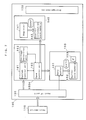
- 100 Storage device
- 110 Host device
- 120 Storage medium
- 140 Control information retaining unit
- 141 Register
- 142 Control information save memory
- 150 Buffer control unit
- 151 Data buffer
- 152 Buffer save memory
- 153 Save flag
- 160 Control unit
- 161 System control unit
- 162 Save control unit
- 163 Voltage detection unit
Claims (16)
Applications Claiming Priority (3)
| Application Number | Priority Date | Filing Date | Title |
|---|---|---|---|
| JP2005-091930 | 2005-03-28 | ||
| JP2005091930 | 2005-03-28 | ||
| PCT/JP2006/305964 WO2006104036A1 (en) | 2005-03-28 | 2006-03-24 | Storage device |
Publications (2)
| Publication Number | Publication Date |
|---|---|
| US20090019194A1 US20090019194A1 (en) | 2009-01-15 |
| US7818477B2 true US7818477B2 (en) | 2010-10-19 |
Family
ID=37053293
Family Applications (1)
| Application Number | Title | Priority Date | Filing Date |
|---|---|---|---|
| US11/909,749 Expired - Fee Related US7818477B2 (en) | 2005-03-28 | 2006-03-24 | Storage device with buffer control unit |
Country Status (3)
| Country | Link |
|---|---|
| US (1) | US7818477B2 (en) |
| JP (1) | JP4881856B2 (en) |
| WO (1) | WO2006104036A1 (en) |
Cited By (2)
| Publication number | Priority date | Publication date | Assignee | Title |
|---|---|---|---|---|
| US20180129416A1 (en) * | 2016-11-04 | 2018-05-10 | Samsung Electronics Co., Ltd. | Storage device and data processing system including the same |
| US10649898B2 (en) | 2017-07-03 | 2020-05-12 | Samsung Electronics Co., Ltd. | Memory system, memory controller for memory system, operation method of memory controller, and operation method of user device including memory device |
Families Citing this family (11)
| Publication number | Priority date | Publication date | Assignee | Title |
|---|---|---|---|---|
| JP5014259B2 (en) * | 2008-05-30 | 2012-08-29 | パナソニック株式会社 | Display control apparatus and display control method |
| JP2010086009A (en) * | 2008-09-29 | 2010-04-15 | Hitachi Ltd | Storage device and memory control method |
| JP2010258608A (en) * | 2009-04-22 | 2010-11-11 | Sony Corp | Imaging apparatus and start-up method of imaging apparatus |
| JP5347779B2 (en) | 2009-07-07 | 2013-11-20 | ソニー株式会社 | MEMORY DEVICE, MEMORY CONTROL METHOD, AND PROGRAM |
| JP5366885B2 (en) * | 2010-05-25 | 2013-12-11 | 日立オートモティブシステムズ株式会社 | Electronic control unit |
| CN102799392B (en) * | 2012-06-16 | 2015-12-16 | 北京忆恒创源科技有限公司 | Memory device and interrupt control method thereof |
| US10643668B1 (en) * | 2013-08-27 | 2020-05-05 | Seagate Technology Llc | Power loss data block marking |
| US9858003B2 (en) * | 2016-05-02 | 2018-01-02 | Toshiba Memory Corporation | Storage system that reliably stores lower page data |
| KR102609473B1 (en) * | 2016-06-17 | 2023-12-04 | 에스케이하이닉스 주식회사 | Data storage device and operating method thereof |
| WO2018166072A1 (en) * | 2017-03-13 | 2018-09-20 | 华为技术有限公司 | Method and device for data processing |
| CN110989918B (en) * | 2018-10-03 | 2023-03-28 | 慧荣科技股份有限公司 | Write control method, data storage device and controller thereof |
Citations (11)
| Publication number | Priority date | Publication date | Assignee | Title |
|---|---|---|---|---|
| JPS6476346A (en) | 1987-09-18 | 1989-03-22 | Fujitsu Ltd | Disk cache control system |
| JPH07200418A (en) | 1993-12-28 | 1995-08-04 | Hitachi Maxell Ltd | Data storage device and its control method |
| US5519831A (en) * | 1991-06-12 | 1996-05-21 | Intel Corporation | Non-volatile disk cache |
| US5596708A (en) * | 1994-04-04 | 1997-01-21 | At&T Global Information Solutions Company | Method and apparatus for the protection of write data in a disk array |
| JPH10154101A (en) | 1996-11-26 | 1998-06-09 | Toshiba Corp | Data storage system and cache controlling method applying to the system |
| US5799200A (en) * | 1995-09-28 | 1998-08-25 | Emc Corporation | Power failure responsive apparatus and method having a shadow dram, a flash ROM, an auxiliary battery, and a controller |
| JPH11143788A (en) | 1997-11-05 | 1999-05-28 | Hitachi Ltd | Outside storage device using non-volatile memory |
| US6289416B1 (en) * | 1997-08-26 | 2001-09-11 | International Business Machines Corporation | Disk drive device and a method for controlling the same |
| US6693840B2 (en) * | 2001-10-17 | 2004-02-17 | Matsushita Electric Industrial Co., Ltd. | Non-volatile semiconductor memory device with enhanced erase/write cycle endurance |
| US6862673B2 (en) * | 2001-11-14 | 2005-03-01 | Silicon Integrated Systems Corporation | Command order maintenance scheme for multi-in/multi-out FIFO in multi-threaded I/O links |
| US7380055B2 (en) * | 2004-06-21 | 2008-05-27 | Dot Hill Systems Corporation | Apparatus and method in a cached raid controller utilizing a solid state backup device for improving data availability time |
-
2006
- 2006-03-24 WO PCT/JP2006/305964 patent/WO2006104036A1/en active Application Filing
- 2006-03-24 JP JP2007510448A patent/JP4881856B2/en not_active Expired - Fee Related
- 2006-03-24 US US11/909,749 patent/US7818477B2/en not_active Expired - Fee Related
Patent Citations (11)
| Publication number | Priority date | Publication date | Assignee | Title |
|---|---|---|---|---|
| JPS6476346A (en) | 1987-09-18 | 1989-03-22 | Fujitsu Ltd | Disk cache control system |
| US5519831A (en) * | 1991-06-12 | 1996-05-21 | Intel Corporation | Non-volatile disk cache |
| JPH07200418A (en) | 1993-12-28 | 1995-08-04 | Hitachi Maxell Ltd | Data storage device and its control method |
| US5596708A (en) * | 1994-04-04 | 1997-01-21 | At&T Global Information Solutions Company | Method and apparatus for the protection of write data in a disk array |
| US5799200A (en) * | 1995-09-28 | 1998-08-25 | Emc Corporation | Power failure responsive apparatus and method having a shadow dram, a flash ROM, an auxiliary battery, and a controller |
| JPH10154101A (en) | 1996-11-26 | 1998-06-09 | Toshiba Corp | Data storage system and cache controlling method applying to the system |
| US6289416B1 (en) * | 1997-08-26 | 2001-09-11 | International Business Machines Corporation | Disk drive device and a method for controlling the same |
| JPH11143788A (en) | 1997-11-05 | 1999-05-28 | Hitachi Ltd | Outside storage device using non-volatile memory |
| US6693840B2 (en) * | 2001-10-17 | 2004-02-17 | Matsushita Electric Industrial Co., Ltd. | Non-volatile semiconductor memory device with enhanced erase/write cycle endurance |
| US6862673B2 (en) * | 2001-11-14 | 2005-03-01 | Silicon Integrated Systems Corporation | Command order maintenance scheme for multi-in/multi-out FIFO in multi-threaded I/O links |
| US7380055B2 (en) * | 2004-06-21 | 2008-05-27 | Dot Hill Systems Corporation | Apparatus and method in a cached raid controller utilizing a solid state backup device for improving data availability time |
Non-Patent Citations (4)
| Title |
|---|
| English language Abstract of JP 10-154101. |
| English language Abstract of JP 11-143788. |
| English language Abstract of JP 64-076346. |
| English language Abstract of JP 7-200418. |
Cited By (3)
| Publication number | Priority date | Publication date | Assignee | Title |
|---|---|---|---|---|
| US20180129416A1 (en) * | 2016-11-04 | 2018-05-10 | Samsung Electronics Co., Ltd. | Storage device and data processing system including the same |
| US10528264B2 (en) * | 2016-11-04 | 2020-01-07 | Samsung Electronics Co., Ltd. | Storage device and data processing system including the same |
| US10649898B2 (en) | 2017-07-03 | 2020-05-12 | Samsung Electronics Co., Ltd. | Memory system, memory controller for memory system, operation method of memory controller, and operation method of user device including memory device |
Also Published As
| Publication number | Publication date |
|---|---|
| JPWO2006104036A1 (en) | 2008-09-04 |
| JP4881856B2 (en) | 2012-02-22 |
| US20090019194A1 (en) | 2009-01-15 |
| WO2006104036A1 (en) | 2006-10-05 |
Similar Documents
| Publication | Publication Date | Title |
|---|---|---|
| US7818477B2 (en) | Storage device with buffer control unit | |
| US8484409B2 (en) | Nonvolatile memory controller with logical defective cluster table | |
| US9495116B2 (en) | Storage device coordinator and a host device that includes the same | |
| US7613871B2 (en) | Storage system using a flash memory partitioned with write-once and rewritable blocks | |
| US20070186040A1 (en) | Memory card, data processor,memory card control method and memory card setting | |
| CN101251826B (en) | Flash memory, method and apparatus for data management of flash memory | |
| KR101115843B1 (en) | Semiconductor memory device | |
| US10152280B2 (en) | Storage device and control method | |
| EP0890955A2 (en) | Storage apparatus, data write-in method, and data read-out method | |
| EP3142014A1 (en) | Method, device and user equipment for reading/writing data in nand flash | |
| US20090313420A1 (en) | Method for saving an address map in a memory device | |
| US8832407B2 (en) | Communication device with storage function | |
| CN110781029A (en) | Power-off protection method and system | |
| CN109426627B (en) | Data storage device and operation method thereof | |
| US20100005229A1 (en) | Flash memory apparatus and method for securing a flash memory from data damage | |
| KR20200043814A (en) | Memory system and operating method thereof | |
| US20230289059A1 (en) | Memory system and operating method thereof | |
| KR102527925B1 (en) | Memory system and operating method thereof | |
| US11803307B2 (en) | Memory system and operating method thereof | |
| JP2007087118A (en) | Controller and portable terminal | |
| US11249895B2 (en) | Memory controller and memory system | |
| JP3017524B2 (en) | Data recording method and IC memory card system in IC memory card | |
| US7330944B2 (en) | Method for storing data in a memory, a system, an electronic device and a memory card | |
| JPH0283645A (en) | Information card controller | |
| KR20150083558A (en) | Method for processing data on storage device and storage device |
Legal Events
| Date | Code | Title | Description |
|---|---|---|---|
| AS | Assignment |
Owner name: MATSUSHITA ELECTRIC INDUSTRIAL CO., LTD., JAPAN Free format text: ASSIGNMENT OF ASSIGNORS INTEREST;ASSIGNORS:TOYAMA, MASAYUKI;NAKANISHI, MASAHIRO;IZUMI, TOMOAKI;AND OTHERS;REEL/FRAME:020200/0165 Effective date: 20071107 |
|
| AS | Assignment |
Owner name: PANASONIC CORPORATION, JAPAN Free format text: CHANGE OF NAME;ASSIGNOR:MATSUSHITA ELECTRIC INDUSTRIAL CO., LTD.;REEL/FRAME:021832/0197 Effective date: 20081001 Owner name: PANASONIC CORPORATION,JAPAN Free format text: CHANGE OF NAME;ASSIGNOR:MATSUSHITA ELECTRIC INDUSTRIAL CO., LTD.;REEL/FRAME:021832/0197 Effective date: 20081001 |
|
| STCF | Information on status: patent grant |
Free format text: PATENTED CASE |
|
| FEPP | Fee payment procedure |
Free format text: PAYOR NUMBER ASSIGNED (ORIGINAL EVENT CODE: ASPN); ENTITY STATUS OF PATENT OWNER: LARGE ENTITY |
|
| FPAY | Fee payment |
Year of fee payment: 4 |
|
| MAFP | Maintenance fee payment |
Free format text: PAYMENT OF MAINTENANCE FEE, 8TH YEAR, LARGE ENTITY (ORIGINAL EVENT CODE: M1552) Year of fee payment: 8 |
|
| FEPP | Fee payment procedure |
Free format text: MAINTENANCE FEE REMINDER MAILED (ORIGINAL EVENT CODE: REM.); ENTITY STATUS OF PATENT OWNER: LARGE ENTITY |
|
| LAPS | Lapse for failure to pay maintenance fees |
Free format text: PATENT EXPIRED FOR FAILURE TO PAY MAINTENANCE FEES (ORIGINAL EVENT CODE: EXP.); ENTITY STATUS OF PATENT OWNER: LARGE ENTITY |
|
| STCH | Information on status: patent discontinuation |
Free format text: PATENT EXPIRED DUE TO NONPAYMENT OF MAINTENANCE FEES UNDER 37 CFR 1.362 |
|
| FP | Lapsed due to failure to pay maintenance fee |
Effective date: 20221019 |