US7835366B2 - Three-way message exchange clock synchronization - Google Patents
Three-way message exchange clock synchronization Download PDFInfo
- Publication number
- US7835366B2 US7835366B2 US11/362,697 US36269706A US7835366B2 US 7835366 B2 US7835366 B2 US 7835366B2 US 36269706 A US36269706 A US 36269706A US 7835366 B2 US7835366 B2 US 7835366B2
- Authority
- US
- United States
- Prior art keywords
- tdm
- segment
- tdm segment
- timestamp
- inter
- Prior art date
- Legal status (The legal status is an assumption and is not a legal conclusion. Google has not performed a legal analysis and makes no representation as to the accuracy of the status listed.)
- Expired - Fee Related, expires
Links
- 238000000034 method Methods 0.000 claims abstract description 26
- 238000011084 recovery Methods 0.000 claims abstract description 9
- 238000005259 measurement Methods 0.000 claims description 7
- 241000238876 Acari Species 0.000 description 16
- 230000003044 adaptive effect Effects 0.000 description 2
- 238000004891 communication Methods 0.000 description 2
- 230000000694 effects Effects 0.000 description 2
- 230000000737 periodic effect Effects 0.000 description 2
- 238000012935 Averaging Methods 0.000 description 1
- 239000000284 extract Substances 0.000 description 1
- 238000012986 modification Methods 0.000 description 1
- 230000004048 modification Effects 0.000 description 1
- 230000001360 synchronised effect Effects 0.000 description 1
- 238000011144 upstream manufacturing Methods 0.000 description 1
Images


Classifications
-
- H—ELECTRICITY
- H04—ELECTRIC COMMUNICATION TECHNIQUE
- H04J—MULTIPLEX COMMUNICATION
- H04J3/00—Time-division multiplex systems
- H04J3/02—Details
- H04J3/06—Synchronising arrangements
- H04J3/0635—Clock or time synchronisation in a network
- H04J3/0638—Clock or time synchronisation among nodes; Internode synchronisation
- H04J3/0647—Synchronisation among TDM nodes
- H04J3/065—Synchronisation among TDM nodes using timestamps
-
- H—ELECTRICITY
- H04—ELECTRIC COMMUNICATION TECHNIQUE
- H04J—MULTIPLEX COMMUNICATION
- H04J3/00—Time-division multiplex systems
- H04J3/02—Details
- H04J3/06—Synchronising arrangements
- H04J3/0635—Clock or time synchronisation in a network
- H04J3/0638—Clock or time synchronisation among nodes; Internode synchronisation
- H04J3/0658—Clock or time synchronisation among packet nodes
- H04J3/0661—Clock or time synchronisation among packet nodes using timestamps
- H04J3/0667—Bidirectional timestamps, e.g. NTP or PTP for compensation of clock drift and for compensation of propagation delays
Definitions
- This invention relates generally to the field of network communications, and more particularly to clock synchronization for Circuit Emulation Service.
- Circuit Emulation Service allows time division multiplexing (“TDM”) services such as DS-n and E-n circuits to be transparently extended across a packet network.
- TDM time division multiplexing
- IP Internet Protocol
- TDM data received from an external device at the edge of an Internet Protocol (“IP”) network is converted to IP packets, sent through the IP network, passed out of the IP network to its destination, and reassembled into a TDM bit stream.
- IP Internet Protocol
- One application of CES is the interconnection of enterprise private telephone networks at different sites. For example, CES over a packet network can be used to connect two private branch exchanges (“PBXs”) on two different campuses without having packet transport capabilities on the PBXs themselves. This inter-working allows voice traffic between the two campuses to use a packet network backbone instead of leased TDM lines, and also allows voice and data traffic to use the same packet network.
- PBXs private branch exchanges
- CMOS complementary metal-oxide-semiconductor
- CMOS complementary metal-oxide-semiconductor
- asynchronous clocking modes include Differential Clock Recovery, Independent Clocking, Clock Recovery using Simple Timestamps, Adaptive Buffer-Fill-based Clock Recovery, and Adaptive Packet Inter-arrival Time Averaging-based Clock Recovery.
- a master periodically sends explicit time indications or timestamps to a slave to enable the slave to synchronize its local clock to the transmitter's clock.
- a high-level view of a clock synchronization scheme based on timestamps is shown in FIG. 1 .
- This synchronization strategy allows multiple slaves, for example in a broadcast or point-to-multipoint communication scenario, to synchronize their clocks to the master.
- the master clock could consist essentially of an oscillator and a pulse counter.
- the oscillator issues periodic pulses that constitute the input to the pulse (timestamp) counter.
- the output of the counter represents the master clock signal and is incremented by a fixed amount at each pulse. Samples of master clock signals are communicated to the slave as timestamps.
- a phase lock loop (“PLL”) at the slave uses the timestamps, which constitute the PLL reference signal, to lock onto the master clock.
- the PLL has four main components: a phase detector, a loop filter, an analog or digitally controlled oscillator, and a timestamp counter.
- the phase detector computes the error signal as the difference between the reference signal and the output signal of the PLL.
- the error signal is passed on to the loop filter which is responsible for eliminating possible jitter and noise in the input signal.
- the controlled oscillator which typically has a center frequency, oscillates at a frequency which is determined by the output signal of the loop filter. However, it would be desirable to reduce PLL input error.
- One advantage of the three-way technique is that it generates lower PLL input errors as compared to the one-way technique. This advantage is in-part a result of employing reverse packet delay variation (“PDV”) to mitigate the effects of the forward PDV on the PLL input error.
- PDV reverse packet delay variation
- FIG. 1 is a high-level view of a prior art clock synchronization scheme based on timestamps.
- FIG. 2 is a high-level view of three-way message exchange for CES.
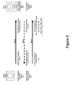
- FIG. 3 illustrates the three phases of the three-way message exchange in greater detail.
- FIG. 4 illustrates operations of the master and slave in greater detail.
- CES can be supported in a network where a TDM transmitter such as a PBX ( 100 ) communicates with a TDM receiver such as a PBX ( 102 ) via a packet network ( 104 ).
- the clock of PBX ( 100 ) is designated as the master clock and the clock of PBX ( 102 ) is designated as the slave clock.
- the PBXs, or other network devices, are operable to facilitate synchronization of the master and slave clocks by exchanging timing information in accordance with a three-way message exchange technique as will be described in detail below.
- the master clock in the three-way message exchange technique may consist essentially of an oscillator and a pulse counter.
- the oscillator issues periodic pulses that constitute the input to the pulse (timestamp) counter.
- the output of the counter represents the master clock signal and is incremented by a fixed amount at each pulse.
- a phase-locked loop (“PLL”) at the slave uses the timestamps to lock onto the master clock.
- the PLL has four main components: a phase detector, a loop filter, an analog or digitally controlled oscillator and a timestamp counter.
- the output of the counter represents the slave clock signal and is incremented by a fixed amount at each pulse.
- the three-way message exchange technique has three phases.
- the error signal is passed on to the loop filter which is responsible for eliminating possible jitter and noise in the input signal.
- the controlled oscillator which typically has a center frequency, oscillates at a frequency which is determined by the output signal of the loop filter.
- ⁇ ⁇ ⁇ T m f ma f sl ⁇ ⁇ ⁇ ⁇ R g + P m
- Case 1 Case 2
- Case 3 Case 4
- Case 5 Case 6 PDV from 0 5 5 8 1 3 Master to Slave, j ms (ms) PDV from Slave 0 5 8 5 3 1 to Master, j sm (ms) PDV from 0 7710 7710 12336 1542 4626 Master to Slave, P ms (clock ticks) PDV from Slave 0 7720 12352 7720 4632 1544 to Master, P sm (clock ticks) Master timestamp 1000 1000 1000 1000 1000 1000 generation interval, ⁇ T g (clock ticks) Slave timestamp 1000 1000 1000 1000 1000 1000 1000 generation interval, ⁇ R g (clock ticks) Master timestamp 1001.3 8721.3 13353.3 8721.3 5633.3 2545.3 inter-arrival interval, ⁇ T m (clock ticks) Slave timestamp 998.71 8708.7 8708.7 13334.7 2540.7 5624.7
Abstract
Description
These definitions yield the results shown in Table 1. It can be observed from these results that the three-way technique generates much lower PLL input errors as compared to the one-way technique. Under packet delay variation (“PDV”) conditions in both directions in a network, the three-way technique is able to use the reverse PDV to mitigate the effects of the forward PDV on the PLL input error.
| TABLE 1 |
| Comparison between the one-way and proposed three-way message |
| Case |
| 1 | |
|
Case 4 | Case 5 | Case 6 |
| PDV from | 0 | 5 | 5 | 8 | 1 | 3 |
| Master to Slave, | ||||||
| jms (ms) | ||||||
| PDV from Slave | 0 | 5 | 8 | 5 | 3 | 1 |
| to Master, jsm | ||||||
| (ms) | ||||||
| PDV from | 0 | 7710 | 7710 | 12336 | 1542 | 4626 |
| Master to Slave, | ||||||
| Pms (clock ticks) | ||||||
| PDV from Slave | 0 | 7720 | 12352 | 7720 | 4632 | 1544 |
| to Master, Psm | ||||||
| (clock ticks) | ||||||
| Master timestamp | 1000 | 1000 | 1000 | 1000 | 1000 | 1000 |
| generation | ||||||
| interval, ΔTg | ||||||
| (clock ticks) | ||||||
| Slave timestamp | 1000 | 1000 | 1000 | 1000 | 1000 | 1000 |
| generation | ||||||
| interval, ΔRg | ||||||
| (clock ticks) | ||||||
| Master timestamp | 1001.3 | 8721.3 | 13353.3 | 8721.3 | 5633.3 | 2545.3 |
| inter-arrival | ||||||
| interval, ΔTm | ||||||
| (clock ticks) | ||||||
| Slave timestamp | 998.71 | 8708.7 | 8708.7 | 13334.7 | 2540.7 | 5624.7 |
| inter-arrival | ||||||
| interval, ΔRm | ||||||
| (clock ticks) | ||||||
| Error in one- | 1.29539 | −7708.7 | −7708.7 | −12334.7 | −1540.7 | −4624.7 |
| way scheme, e1 | ||||||
| (clock ticks) | ||||||
| Error in three- | 1.29618 | 6.29618 | 2322.3 | −2306.7 | 1546.3 | −1539.7 |
| way scheme e3, | ||||||
| (clock ticks) | ||||||
|
|
0.000648088 | 1225.35 | 4.31943 | 4.34733 | 1.99638 | 2.00363 |
Claims (20)
Priority Applications (2)
| Application Number | Priority Date | Filing Date | Title |
|---|---|---|---|
| US11/362,697 US7835366B2 (en) | 2005-11-01 | 2006-02-27 | Three-way message exchange clock synchronization |
| PCT/CA2006/001555 WO2007051283A1 (en) | 2005-11-01 | 2006-09-21 | Three-way message exchange clock synchronization |
Applications Claiming Priority (2)
| Application Number | Priority Date | Filing Date | Title |
|---|---|---|---|
| US73227605P | 2005-11-01 | 2005-11-01 | |
| US11/362,697 US7835366B2 (en) | 2005-11-01 | 2006-02-27 | Three-way message exchange clock synchronization |
Publications (2)
| Publication Number | Publication Date |
|---|---|
| US20070097947A1 US20070097947A1 (en) | 2007-05-03 |
| US7835366B2 true US7835366B2 (en) | 2010-11-16 |
Family
ID=37996176
Family Applications (1)
| Application Number | Title | Priority Date | Filing Date |
|---|---|---|---|
| US11/362,697 Expired - Fee Related US7835366B2 (en) | 2005-11-01 | 2006-02-27 | Three-way message exchange clock synchronization |
Country Status (2)
| Country | Link |
|---|---|
| US (1) | US7835366B2 (en) |
| WO (1) | WO2007051283A1 (en) |
Cited By (4)
| Publication number | Priority date | Publication date | Assignee | Title |
|---|---|---|---|---|
| US9432144B2 (en) | 2014-09-12 | 2016-08-30 | Ciena Corporation | Precision time transfer systems and methods in optical networks |
| US10594395B2 (en) | 2018-07-23 | 2020-03-17 | Ciena Corporation | Systems and methods for compensating coherent optics delay asymmetry in a packet optical network |
| US20200228305A1 (en) * | 2019-01-10 | 2020-07-16 | Fujitsu Limited | Information processing apparatus, time synchronization method, and computer-readable recording medium recording time synchronization program |
| US11552722B2 (en) | 2020-12-10 | 2023-01-10 | Ciena Corporation | Precision time protocol using a coherent optical DSP frame |
Families Citing this family (14)
| Publication number | Priority date | Publication date | Assignee | Title |
|---|---|---|---|---|
| US7492732B2 (en) * | 2005-11-01 | 2009-02-17 | Nortel Networks Limited | Differential clock recovery in packet networks |
| US7742505B2 (en) * | 2005-12-14 | 2010-06-22 | Adtran, Inc. | Systems and methods for enabling clock signal synchronization |
| GB2443867A (en) * | 2006-03-21 | 2008-05-21 | Zarlink Semiconductor Ltd | Timing source with packet size controller providing a distribution of packet sizes |
| CN101459500B (en) * | 2007-12-14 | 2011-11-16 | 华为技术有限公司 | Method for implementing time master-slave protection and time master-slave protection device |
| FR2951598B1 (en) * | 2009-10-15 | 2016-02-12 | Sagem Comm | IP AND RADIO COMMUNICATION DEVICE WITH A SINGLE OSCILLATOR AND METHOD OF CONTROLLING THE OSCILLATOR |
| CN102111258A (en) * | 2009-12-25 | 2011-06-29 | 华为技术有限公司 | Clock synchronization method, equipment and system |
| EP2341649B1 (en) * | 2010-01-04 | 2012-09-19 | Alcatel Lucent | Frequency synchronization method and system in a communication network |
| GB201002401D0 (en) * | 2010-02-12 | 2010-03-31 | Zarlink Semiconductor Inc | Feedforward synchronization in asynchronous packet networks |
| US8693608B2 (en) * | 2010-09-20 | 2014-04-08 | Alcatel Lucent | Frequency synchronization using clock recovery loop with adaptive packet filtering |
| US9014215B2 (en) | 2011-09-22 | 2015-04-21 | Aviat U.S., Inc. | Systems and methods for synchronization of clock signals |
| EP3044891B1 (en) * | 2013-09-11 | 2019-12-25 | Khalifa University of Science and Technology | Method and devices for frequency distribution |
| US9112628B2 (en) * | 2013-10-02 | 2015-08-18 | Khalifa University of Science, Technology, and Research | Method and devices for compensating for path asymmetry |
| US9531395B2 (en) * | 2013-10-02 | 2016-12-27 | Khalifa University Of Science, Technology And Research | Method and devices for time and frequency synchronization using a phase locked loop |
| EP3053289B1 (en) * | 2013-10-02 | 2019-12-18 | Khalifa University of Science and Technology | Method and devices for compensating for path asymmetry |
Citations (18)
| Publication number | Priority date | Publication date | Assignee | Title |
|---|---|---|---|---|
| US5815689A (en) * | 1997-04-04 | 1998-09-29 | Microsoft Corporation | Method and computer program product for synchronizing the processing of multiple data streams and matching disparate processing rates using a standardized clock mechanism |
| US5970107A (en) * | 1998-01-06 | 1999-10-19 | Maker Communications, Inc. | Synchronous residual time stamp service clock regenerator phase locked loop phase comparator and loop filter |
| US6199169B1 (en) * | 1998-03-31 | 2001-03-06 | Compaq Computer Corporation | System and method for synchronizing time across a computer cluster |
| US20020027886A1 (en) * | 2000-04-07 | 2002-03-07 | Fischer Matthew James | Method of controlling data sampling clocking of asynchronous network nodes in a frame-based communications network |
| US6449291B1 (en) * | 1998-11-24 | 2002-09-10 | 3Com Corporation | Method and apparatus for time synchronization in a communication system |
| US6496553B1 (en) | 1997-12-19 | 2002-12-17 | Nec Corporation | PLL for reproducing standard clock from random time information |
| EP1294116A2 (en) | 2001-09-18 | 2003-03-19 | Nortel Networks Limited | Technique for synchronizing clocks in a network |
| US20040062278A1 (en) | 2002-09-30 | 2004-04-01 | Lucent Technologies, Inc. | Systems and methods for synchronization in asynchronous transport networks |
| US20040114632A1 (en) * | 2002-11-29 | 2004-06-17 | Fumio Yuuki | Clock and data recovery method and digital circuit for the same |
| US20050100054A1 (en) * | 2002-08-24 | 2005-05-12 | Scott Martin R. | Adaptive clock recovery |
| US6898213B1 (en) | 2000-10-16 | 2005-05-24 | Iprad Ltd. | Circuit emulation service (CES) over IP |
| US20050207387A1 (en) * | 2004-02-09 | 2005-09-22 | Semtech Corporation | Method and apparatus for aligning time references when separated by an unreliable data packet network |
| US6980586B1 (en) * | 1999-05-24 | 2005-12-27 | Intel Corporation | Pseudo-noise encoded digital data clock recovery |
| US7010074B2 (en) * | 2001-01-11 | 2006-03-07 | Nec Electronics Corporation | Oversampling clock recovery having a high follow-up character using a few clock signals |
| US7114091B2 (en) * | 2002-03-18 | 2006-09-26 | National Instruments Corporation | Synchronization of distributed systems |
| US20060245453A1 (en) * | 2005-04-27 | 2006-11-02 | Bedrosian P S | Line-timing in packet-based networks |
| US7203240B2 (en) * | 2003-05-16 | 2007-04-10 | Samsung Electronics Co., Ltd. | Method of recovering clock signal using user clock code in TDM digital video signal and transmitting/receiving apparatus used for the method |
| US7379480B2 (en) * | 2003-01-16 | 2008-05-27 | Rockwell Automation Technologies, Inc. | Fast frequency adjustment method for synchronizing network clocks |
Family Cites Families (1)
| Publication number | Priority date | Publication date | Assignee | Title |
|---|---|---|---|---|
| US6898313B2 (en) * | 2002-03-06 | 2005-05-24 | Sharp Laboratories Of America, Inc. | Scalable layered coding in a multi-layer, compound-image data transmission system |
-
2006
- 2006-02-27 US US11/362,697 patent/US7835366B2/en not_active Expired - Fee Related
- 2006-09-21 WO PCT/CA2006/001555 patent/WO2007051283A1/en active Application Filing
Patent Citations (20)
| Publication number | Priority date | Publication date | Assignee | Title |
|---|---|---|---|---|
| US5815689A (en) * | 1997-04-04 | 1998-09-29 | Microsoft Corporation | Method and computer program product for synchronizing the processing of multiple data streams and matching disparate processing rates using a standardized clock mechanism |
| US6496553B1 (en) | 1997-12-19 | 2002-12-17 | Nec Corporation | PLL for reproducing standard clock from random time information |
| US5970107A (en) * | 1998-01-06 | 1999-10-19 | Maker Communications, Inc. | Synchronous residual time stamp service clock regenerator phase locked loop phase comparator and loop filter |
| US6199169B1 (en) * | 1998-03-31 | 2001-03-06 | Compaq Computer Corporation | System and method for synchronizing time across a computer cluster |
| US6449291B1 (en) * | 1998-11-24 | 2002-09-10 | 3Com Corporation | Method and apparatus for time synchronization in a communication system |
| US6980586B1 (en) * | 1999-05-24 | 2005-12-27 | Intel Corporation | Pseudo-noise encoded digital data clock recovery |
| US20020027886A1 (en) * | 2000-04-07 | 2002-03-07 | Fischer Matthew James | Method of controlling data sampling clocking of asynchronous network nodes in a frame-based communications network |
| US6898213B1 (en) | 2000-10-16 | 2005-05-24 | Iprad Ltd. | Circuit emulation service (CES) over IP |
| US7010074B2 (en) * | 2001-01-11 | 2006-03-07 | Nec Electronics Corporation | Oversampling clock recovery having a high follow-up character using a few clock signals |
| EP1294116A2 (en) | 2001-09-18 | 2003-03-19 | Nortel Networks Limited | Technique for synchronizing clocks in a network |
| US20030056136A1 (en) * | 2001-09-18 | 2003-03-20 | James Aweya | Technique for synchronizing clocks in a network |
| US7114091B2 (en) * | 2002-03-18 | 2006-09-26 | National Instruments Corporation | Synchronization of distributed systems |
| US20050100054A1 (en) * | 2002-08-24 | 2005-05-12 | Scott Martin R. | Adaptive clock recovery |
| US20040062278A1 (en) | 2002-09-30 | 2004-04-01 | Lucent Technologies, Inc. | Systems and methods for synchronization in asynchronous transport networks |
| US7372875B2 (en) * | 2002-09-30 | 2008-05-13 | Lucent Technologies Inc. | Systems and methods for synchronization in asynchronous transport networks |
| US20040114632A1 (en) * | 2002-11-29 | 2004-06-17 | Fumio Yuuki | Clock and data recovery method and digital circuit for the same |
| US7379480B2 (en) * | 2003-01-16 | 2008-05-27 | Rockwell Automation Technologies, Inc. | Fast frequency adjustment method for synchronizing network clocks |
| US7203240B2 (en) * | 2003-05-16 | 2007-04-10 | Samsung Electronics Co., Ltd. | Method of recovering clock signal using user clock code in TDM digital video signal and transmitting/receiving apparatus used for the method |
| US20050207387A1 (en) * | 2004-02-09 | 2005-09-22 | Semtech Corporation | Method and apparatus for aligning time references when separated by an unreliable data packet network |
| US20060245453A1 (en) * | 2005-04-27 | 2006-11-02 | Bedrosian P S | Line-timing in packet-based networks |
Non-Patent Citations (1)
| Title |
|---|
| Mills, Improved Algorithms for Synchronizing Computer Network Clocks, IEEE/ACM Transactions on Networking, Jun. 1995, pp. 245-254, vol. 3, No. 3. * |
Cited By (5)
| Publication number | Priority date | Publication date | Assignee | Title |
|---|---|---|---|---|
| US9432144B2 (en) | 2014-09-12 | 2016-08-30 | Ciena Corporation | Precision time transfer systems and methods in optical networks |
| US10594395B2 (en) | 2018-07-23 | 2020-03-17 | Ciena Corporation | Systems and methods for compensating coherent optics delay asymmetry in a packet optical network |
| US20200228305A1 (en) * | 2019-01-10 | 2020-07-16 | Fujitsu Limited | Information processing apparatus, time synchronization method, and computer-readable recording medium recording time synchronization program |
| US10771232B2 (en) * | 2019-01-10 | 2020-09-08 | Fujitsu Limited | Information processing apparatus, time synchronization method, and computer-readable recording medium recording time synchronization program |
| US11552722B2 (en) | 2020-12-10 | 2023-01-10 | Ciena Corporation | Precision time protocol using a coherent optical DSP frame |
Also Published As
| Publication number | Publication date |
|---|---|
| WO2007051283A1 (en) | 2007-05-10 |
| US20070097947A1 (en) | 2007-05-03 |
Similar Documents
| Publication | Publication Date | Title |
|---|---|---|
| US7835366B2 (en) | Three-way message exchange clock synchronization | |
| US8774227B2 (en) | Multi input timing recovery over packet network | |
| US7492732B2 (en) | Differential clock recovery in packet networks | |
| US7043651B2 (en) | Technique for synchronizing clocks in a network | |
| US6438702B1 (en) | Method for providing a precise network time service | |
| EP1940086B1 (en) | Method, ethernet device and ethernet for solving the clock synchronization | |
| US7356036B2 (en) | Method providing distribution means for reference clocks across packetized networks | |
| US8126333B2 (en) | Optical transmission system and synchronization method using time reference pulse | |
| US8018968B2 (en) | System and method for high precision clock recovery over packet networks | |
| US7483450B1 (en) | Method and system for link-based clock synchronization in asynchronous networks | |
| EP2580883B1 (en) | Node and system for a synchronous network | |
| US7535931B1 (en) | Two-way timing protocol | |
| Lv et al. | An enhanced IEEE 1588 time synchronization for asymmetric communication link in packet transport network | |
| US8571068B2 (en) | Network timing distribution and synchronization using virtual network delays | |
| US20110051754A1 (en) | Measurement and adjustment of real-time values according to residence time in networking equipment without access to real time | |
| JP2006503480A (en) | System and method for synchronizing communication terminals in an asynchronous network using time stamps | |
| CN102013931A (en) | Time synchronization method and system, salve timing device and main timing device | |
| US10355799B2 (en) | Pseudowire clock recovery | |
| WO2012065334A1 (en) | Method, device and system for realizing time synchronization in time division multiplexing network | |
| US20080159270A1 (en) | Integrated phase lock loop and network phy or switch | |
| US7688862B2 (en) | Systems and methods for the synchronization of a real-time scheduled packet network using relative timing | |
| JP2001513301A (en) | Synchronization in ATM by STM transmission system | |
| US6198736B1 (en) | Telecommunications system | |
| KR20160024782A (en) | network synchronization apparatus and method on passive optical access network | |
| Keten | GPS/GNSS independent Time Transfer over Telco IP Core Networks using DTM overlay |
Legal Events
| Date | Code | Title | Description |
|---|---|---|---|
| AS | Assignment |
Owner name: NORTEL NETWORKS LIMITED, CANADA Free format text: ASSIGNMENT OF ASSIGNORS INTEREST;ASSIGNORS:AWEYA, JAMES;OUELLETTE, MICHEL;MONTUNO, DELFIN;AND OTHERS;SIGNING DATES FROM 20060220 TO 20060221;REEL/FRAME:017630/0099 Owner name: NORTEL NETWORKS LIMITED, CANADA Free format text: ASSIGNMENT OF ASSIGNORS INTEREST;ASSIGNORS:AWEYA, JAMES;OUELLETTE, MICHEL;MONTUNO, DELFIN;AND OTHERS;REEL/FRAME:017630/0099;SIGNING DATES FROM 20060220 TO 20060221 |
|
| FEPP | Fee payment procedure |
Free format text: PAYOR NUMBER ASSIGNED (ORIGINAL EVENT CODE: ASPN); ENTITY STATUS OF PATENT OWNER: LARGE ENTITY |
|
| AS | Assignment |
Owner name: CIENA LUXEMBOURG S.A.R.L.,LUXEMBOURG Free format text: ASSIGNMENT OF ASSIGNORS INTEREST;ASSIGNOR:NORTEL NETWORKS LIMITED;REEL/FRAME:024213/0653 Effective date: 20100319 Owner name: CIENA LUXEMBOURG S.A.R.L., LUXEMBOURG Free format text: ASSIGNMENT OF ASSIGNORS INTEREST;ASSIGNOR:NORTEL NETWORKS LIMITED;REEL/FRAME:024213/0653 Effective date: 20100319 |
|
| AS | Assignment |
Owner name: CIENA CORPORATION,MARYLAND Free format text: ASSIGNMENT OF ASSIGNORS INTEREST;ASSIGNOR:CIENA LUXEMBOURG S.A.R.L.;REEL/FRAME:024252/0060 Effective date: 20100319 Owner name: CIENA CORPORATION, MARYLAND Free format text: ASSIGNMENT OF ASSIGNORS INTEREST;ASSIGNOR:CIENA LUXEMBOURG S.A.R.L.;REEL/FRAME:024252/0060 Effective date: 20100319 |
|
| STCF | Information on status: patent grant |
Free format text: PATENTED CASE |
|
| FPAY | Fee payment |
Year of fee payment: 4 |
|
| AS | Assignment |
Owner name: DEUTSCHE BANK AG NEW YORK BRANCH, NEW YORK Free format text: SECURITY INTEREST;ASSIGNOR:CIENA CORPORATION;REEL/FRAME:033329/0417 Effective date: 20140715 |
|
| AS | Assignment |
Owner name: BANK OF AMERICA, N.A., AS ADMINISTRATIVE AGENT, NO Free format text: PATENT SECURITY AGREEMENT;ASSIGNOR:CIENA CORPORATION;REEL/FRAME:033347/0260 Effective date: 20140715 |
|
| FEPP | Fee payment procedure |
Free format text: PAYER NUMBER DE-ASSIGNED (ORIGINAL EVENT CODE: RMPN); ENTITY STATUS OF PATENT OWNER: LARGE ENTITY Free format text: PAYOR NUMBER ASSIGNED (ORIGINAL EVENT CODE: ASPN); ENTITY STATUS OF PATENT OWNER: LARGE ENTITY |
|
| MAFP | Maintenance fee payment |
Free format text: PAYMENT OF MAINTENANCE FEE, 8TH YEAR, LARGE ENTITY (ORIGINAL EVENT CODE: M1552) Year of fee payment: 8 |
|
| AS | Assignment |
Owner name: CIENA CORPORATION, MARYLAND Free format text: RELEASE BY SECURED PARTY;ASSIGNOR:DEUTSCHE BANK AG NEW YORK BRANCH;REEL/FRAME:050938/0389 Effective date: 20191028 |
|
| AS | Assignment |
Owner name: BANK OF AMERICA, N.A., AS COLLATERAL AGENT, ILLINO Free format text: PATENT SECURITY AGREEMENT;ASSIGNOR:CIENA CORPORATION;REEL/FRAME:050969/0001 Effective date: 20191028 |
|
| FEPP | Fee payment procedure |
Free format text: MAINTENANCE FEE REMINDER MAILED (ORIGINAL EVENT CODE: REM.); ENTITY STATUS OF PATENT OWNER: LARGE ENTITY |
|
| LAPS | Lapse for failure to pay maintenance fees |
Free format text: PATENT EXPIRED FOR FAILURE TO PAY MAINTENANCE FEES (ORIGINAL EVENT CODE: EXP.); ENTITY STATUS OF PATENT OWNER: LARGE ENTITY |
|
| STCH | Information on status: patent discontinuation |
Free format text: PATENT EXPIRED DUE TO NONPAYMENT OF MAINTENANCE FEES UNDER 37 CFR 1.362 |
|
| FP | Lapsed due to failure to pay maintenance fee |
Effective date: 20221116 |
|
| AS | Assignment |
Owner name: CIENA CORPORATION, MARYLAND Free format text: RELEASE BY SECURED PARTY;ASSIGNOR:BANK OF AMERICA, N.A.;REEL/FRAME:065630/0232 Effective date: 20231024 |