US7842356B2 - Substrate processing methods - Google Patents
Substrate processing methods Download PDFInfo
- Publication number
- US7842356B2 US7842356B2 US11/453,077 US45307706A US7842356B2 US 7842356 B2 US7842356 B2 US 7842356B2 US 45307706 A US45307706 A US 45307706A US 7842356 B2 US7842356 B2 US 7842356B2
- Authority
- US
- United States
- Prior art keywords
- substrate
- insulating film
- gas
- process vessel
- plasma
- Prior art date
- Legal status (The legal status is an assumption and is not a legal conclusion. Google has not performed a legal analysis and makes no representation as to the accuracy of the status listed.)
- Expired - Fee Related, expires
Links
Images


Classifications
-
- H—ELECTRICITY
- H01—ELECTRIC ELEMENTS
- H01L—SEMICONDUCTOR DEVICES NOT COVERED BY CLASS H10
- H01L21/00—Processes or apparatus adapted for the manufacture or treatment of semiconductor or solid state devices or of parts thereof
- H01L21/02—Manufacture or treatment of semiconductor devices or of parts thereof
- H01L21/04—Manufacture or treatment of semiconductor devices or of parts thereof the devices having at least one potential-jump barrier or surface barrier, e.g. PN junction, depletion layer or carrier concentration layer
- H01L21/18—Manufacture or treatment of semiconductor devices or of parts thereof the devices having at least one potential-jump barrier or surface barrier, e.g. PN junction, depletion layer or carrier concentration layer the devices having semiconductor bodies comprising elements of Group IV of the Periodic System or AIIIBV compounds with or without impurities, e.g. doping materials
- H01L21/20—Deposition of semiconductor materials on a substrate, e.g. epitaxial growth solid phase epitaxy
-
- C—CHEMISTRY; METALLURGY
- C23—COATING METALLIC MATERIAL; COATING MATERIAL WITH METALLIC MATERIAL; CHEMICAL SURFACE TREATMENT; DIFFUSION TREATMENT OF METALLIC MATERIAL; COATING BY VACUUM EVAPORATION, BY SPUTTERING, BY ION IMPLANTATION OR BY CHEMICAL VAPOUR DEPOSITION, IN GENERAL; INHIBITING CORROSION OF METALLIC MATERIAL OR INCRUSTATION IN GENERAL
- C23C—COATING METALLIC MATERIAL; COATING MATERIAL WITH METALLIC MATERIAL; SURFACE TREATMENT OF METALLIC MATERIAL BY DIFFUSION INTO THE SURFACE, BY CHEMICAL CONVERSION OR SUBSTITUTION; COATING BY VACUUM EVAPORATION, BY SPUTTERING, BY ION IMPLANTATION OR BY CHEMICAL VAPOUR DEPOSITION, IN GENERAL
- C23C16/00—Chemical coating by decomposition of gaseous compounds, without leaving reaction products of surface material in the coating, i.e. chemical vapour deposition [CVD] processes
- C23C16/22—Chemical coating by decomposition of gaseous compounds, without leaving reaction products of surface material in the coating, i.e. chemical vapour deposition [CVD] processes characterised by the deposition of inorganic material, other than metallic material
- C23C16/26—Deposition of carbon only
-
- C—CHEMISTRY; METALLURGY
- C23—COATING METALLIC MATERIAL; COATING MATERIAL WITH METALLIC MATERIAL; CHEMICAL SURFACE TREATMENT; DIFFUSION TREATMENT OF METALLIC MATERIAL; COATING BY VACUUM EVAPORATION, BY SPUTTERING, BY ION IMPLANTATION OR BY CHEMICAL VAPOUR DEPOSITION, IN GENERAL; INHIBITING CORROSION OF METALLIC MATERIAL OR INCRUSTATION IN GENERAL
- C23C—COATING METALLIC MATERIAL; COATING MATERIAL WITH METALLIC MATERIAL; SURFACE TREATMENT OF METALLIC MATERIAL BY DIFFUSION INTO THE SURFACE, BY CHEMICAL CONVERSION OR SUBSTITUTION; COATING BY VACUUM EVAPORATION, BY SPUTTERING, BY ION IMPLANTATION OR BY CHEMICAL VAPOUR DEPOSITION, IN GENERAL
- C23C16/00—Chemical coating by decomposition of gaseous compounds, without leaving reaction products of surface material in the coating, i.e. chemical vapour deposition [CVD] processes
- C23C16/44—Chemical coating by decomposition of gaseous compounds, without leaving reaction products of surface material in the coating, i.e. chemical vapour deposition [CVD] processes characterised by the method of coating
- C23C16/448—Chemical coating by decomposition of gaseous compounds, without leaving reaction products of surface material in the coating, i.e. chemical vapour deposition [CVD] processes characterised by the method of coating characterised by the method used for generating reactive gas streams, e.g. by evaporation or sublimation of precursor materials
- C23C16/452—Chemical coating by decomposition of gaseous compounds, without leaving reaction products of surface material in the coating, i.e. chemical vapour deposition [CVD] processes characterised by the method of coating characterised by the method used for generating reactive gas streams, e.g. by evaporation or sublimation of precursor materials by activating reactive gas streams before their introduction into the reaction chamber, e.g. by ionisation or addition of reactive species
-
- H—ELECTRICITY
- H01—ELECTRIC ELEMENTS
- H01J—ELECTRIC DISCHARGE TUBES OR DISCHARGE LAMPS
- H01J37/00—Discharge tubes with provision for introducing objects or material to be exposed to the discharge, e.g. for the purpose of examination or processing thereof
- H01J37/32—Gas-filled discharge tubes
- H01J37/32009—Arrangements for generation of plasma specially adapted for examination or treatment of objects, e.g. plasma sources
- H01J37/32192—Microwave generated discharge
-
- H—ELECTRICITY
- H01—ELECTRIC ELEMENTS
- H01L—SEMICONDUCTOR DEVICES NOT COVERED BY CLASS H10
- H01L21/00—Processes or apparatus adapted for the manufacture or treatment of semiconductor or solid state devices or of parts thereof
- H01L21/02—Manufacture or treatment of semiconductor devices or of parts thereof
- H01L21/02104—Forming layers
- H01L21/02107—Forming insulating materials on a substrate
- H01L21/02109—Forming insulating materials on a substrate characterised by the type of layer, e.g. type of material, porous/non-porous, pre-cursors, mixtures or laminates
- H01L21/02112—Forming insulating materials on a substrate characterised by the type of layer, e.g. type of material, porous/non-porous, pre-cursors, mixtures or laminates characterised by the material of the layer
- H01L21/02115—Forming insulating materials on a substrate characterised by the type of layer, e.g. type of material, porous/non-porous, pre-cursors, mixtures or laminates characterised by the material of the layer the material being carbon, e.g. alpha-C, diamond or hydrogen doped carbon
-
- H—ELECTRICITY
- H01—ELECTRIC ELEMENTS
- H01L—SEMICONDUCTOR DEVICES NOT COVERED BY CLASS H10
- H01L21/00—Processes or apparatus adapted for the manufacture or treatment of semiconductor or solid state devices or of parts thereof
- H01L21/02—Manufacture or treatment of semiconductor devices or of parts thereof
- H01L21/04—Manufacture or treatment of semiconductor devices or of parts thereof the devices having at least one potential-jump barrier or surface barrier, e.g. PN junction, depletion layer or carrier concentration layer
- H01L21/18—Manufacture or treatment of semiconductor devices or of parts thereof the devices having at least one potential-jump barrier or surface barrier, e.g. PN junction, depletion layer or carrier concentration layer the devices having semiconductor bodies comprising elements of Group IV of the Periodic System or AIIIBV compounds with or without impurities, e.g. doping materials
- H01L21/30—Treatment of semiconductor bodies using processes or apparatus not provided for in groups H01L21/20 - H01L21/26
- H01L21/31—Treatment of semiconductor bodies using processes or apparatus not provided for in groups H01L21/20 - H01L21/26 to form insulating layers thereon, e.g. for masking or by using photolithographic techniques; After treatment of these layers; Selection of materials for these layers
- H01L21/314—Inorganic layers
- H01L21/3146—Carbon layers, e.g. diamond-like layers
-
- H—ELECTRICITY
- H01—ELECTRIC ELEMENTS
- H01L—SEMICONDUCTOR DEVICES NOT COVERED BY CLASS H10
- H01L21/00—Processes or apparatus adapted for the manufacture or treatment of semiconductor or solid state devices or of parts thereof
- H01L21/02—Manufacture or treatment of semiconductor devices or of parts thereof
- H01L21/02104—Forming layers
- H01L21/02107—Forming insulating materials on a substrate
- H01L21/02225—Forming insulating materials on a substrate characterised by the process for the formation of the insulating layer
- H01L21/0226—Forming insulating materials on a substrate characterised by the process for the formation of the insulating layer formation by a deposition process
- H01L21/02263—Forming insulating materials on a substrate characterised by the process for the formation of the insulating layer formation by a deposition process deposition from the gas or vapour phase
- H01L21/02271—Forming insulating materials on a substrate characterised by the process for the formation of the insulating layer formation by a deposition process deposition from the gas or vapour phase deposition by decomposition or reaction of gaseous or vapour phase compounds, i.e. chemical vapour deposition
- H01L21/02274—Forming insulating materials on a substrate characterised by the process for the formation of the insulating layer formation by a deposition process deposition from the gas or vapour phase deposition by decomposition or reaction of gaseous or vapour phase compounds, i.e. chemical vapour deposition in the presence of a plasma [PECVD]
Definitions
- the present invention relates to a substrate processing method, a computer readable recording medium and a substrate processing apparatus.
- an interlayer insulating film for example, to insulate between wirings is formed on a substrate.
- an interlayer insulating film with low dielectric constant has been advanced to realize further elimination of a resistance and a capacitance of this wiring portion.
- a polymeric film containing fluorine has attracted attention as a film material of the insulating film capable of realizing the low dielectric constant.
- this polymeric film when this polymeric film is used, there is a possibility that a fluorine atom within the film reacts with surrounding moisture while a substrate is processed, and hydrogen fluoride gas is emitted from inside of the film to destruct and peel off peripheral films. Consequently, it is proposed that amorphous carbon in which the same degree of low dielectric constant can be obtained is used as the film material of the insulating film instead of the polymeric film containing fluorine.
- a method is proposed as a deposition method of amorphous carbon, in which cyclic hydrocarbon gas is supplied into a chamber and a plasma is generated inside of the chamber to thereby from a film by using a parallel plate type plasma CVD apparatus (refer to U.S. Pat. No. 5,981,000).
- a parallel plate type plasma CVD apparatus a parallel plate type plasma CVD apparatus
- a bias voltage is applied to a substrate inside of the chamber, charged particles within the plasma are attracted to a surface of the substrate, and thereby, an insulating film is formed on the substrate.
- a value of a dielectric constant (k value) of the insulating film was approximately 3.5. It is necessary to realize the insulating film having lower dielectric constant to realize a high speed and low power consumption of the electronic device. Besides, when the above-stated deposition method is used, a heat resistance of the film is bad, and therefore a film thickness may vary or a film quality may deteriorate, for example, at a heating process of the substrate.
- the present invention is made in consideration of these points, and an object thereof is to form an insulating film of amorphous carbon having lower dielectric constant and better heat resistance.
- a substrate processing method including the step of: forming an insulating film of amorphous carbon on a substrate by supplying hydrocarbon gas having a multiple bond into a process vessel in which the substrate is accommodated, and generating a plasma inside of the process vessel.
- the insulating film of amorphous carbon of which dielectric constant is approximately 2.5 is formed by using the substrate processing method according to the present invention. Besides, the insulating film having a significantly high heat resistance is formed by the present invention. As stated above, according to the present invention, the insulating film of amorphous carbon having the lower dielectric constant and higher heat resistance compared to the prior art can be formed.
- the hydrocarbon gas is acetylene gas
- hydrogen gas may be supplied into the process vessel in addition to the acetylene gas.
- the acetylene gas and the hydrogen gas may be supplied with a volume ratio of 4:3 to 4:1. A leak current of the insulating film can be eliminated by this process.
- the hydrocarbon gas may be butyne gas.
- a pressure inside of the process vessel may be maintained to be 4.0 Pa or less while the insulating film is formed.
- the substrate may be maintained to be 200° C. or less while the insulating film is formed.
- the substrate may be heated in an atmosphere containing the hydrogen gas after the insulating film is formed.
- the dielectric constant of the insulating film is further eliminated, and the insulating film with little leak current and good heat resistance can be formed.
- the substrate may be heated at the temperature of 350° C. to 400° C. after the insulating film is formed.
- the substrate may be maintained in the atmosphere not containing oxygen during a period after the insulating film is formed until the substrate is heated.
- the plasma may be generated inside of the process vessel by using a microwave.
- inside of the process vessel may be sectionalized into a plasma generation region in which the plasma is generated, and a film formation region in which the insulating film is formed on the substrate by using the plasma generated in the plasma generation region, plasma gas for plasma generation may be supplied to the plasma generation region, and the hydrocarbon gas may be supplied to the film formation region.
- the plasma may be generated inside of the process vessel under a state in which a bias voltage is not applied to the substrate inside of the process vessel.
- Another aspect of the present invention is a computer readable recording medium recording a program for causing a computer to realize the above-stated substrate processing method.
- Another aspect of the present invention is a substrate processing apparatus, including: a control portion performing the substrate processing method.
- the insulating film having low dielectric constant and good heat resistance is realized, and therefore, an electronic device which has higher speed and lower power consumption can be manufactured.
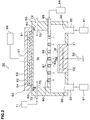
- FIG. 1 is an explanatory view schematically showing an outline of a constitution of a substrate processing apparatus in an embodiment
- FIG. 2 is an explanatory view of a vertical section showing an outline of a constitution of an insulating film forming apparatus
- FIG. 3 is a plan view of a source gas supply structure
- FIG. 4 is an explanatory view of a vertical section showing an outline of a constitution of an annealing apparatus
- FIG. 5 is an explanatory view of a vertical section showing an outline of a constitution of an insulating film forming apparatus including a gas supply source of hydrogen gas;
- FIG. 6 is a graphic chart showing a relation of a mixing ratio of the hydrogen gas, a leak current and a shrinkage
- FIG. 7 is an explanatory view of a vertical section showing an outline of a constitution of an annealing apparatus including a gas supply source of the hydrogen gas;
- FIG. 8 is a graphic chart showing a relation of a pressure inside of a process vessel, a shrinkage and a deposition rate at a time of a deposition
- FIG. 9 is a graphic chart showing a leak current relative to each applied voltage as for an insulating film in which the hydrogen gas is supplied at a time of an annealing process.
- FIG. 10 is a graphic chart showing a leak current relative to each applied voltage as for an insulating film formed by a conventional substrate process.
- FIG. 1 is a plan view showing an outline of a constitution of a substrate processing apparatus 1 in which a substrate processing method according to the present invention is performed.
- the substrate processing apparatus 1 has a constitution in which a cassette station 2 , for example, carrying in/out plural substrates W to the substrate processing apparatus 1 from external per cassette as a unit and carrying in/out the substrate W to a cassette C, and a processing station 3 including plural various apparatuses processing the substrates W in sheet-fed mode are connected integrally in Y direction (horizontal direction in the drawing).
- the cassette station 2 is composed of a cassette mounting table 4 and a carrier chamber 5 .
- the carrier chamber 5 includes a substrate carrier 6 composed of, for example, a multi-joint robot, and a pre-alignment stage 7 .
- the substrate carrier 6 is able to carry the substrate W to the cassettes C on the cassette mounting table 4 , the pre-alignment stage 7 , and later-described load lock chambers 30 , 31 of the processing station 3 .
- the processing station 3 includes a carrier path 8 formed in linear state from the cassette station 2 in Y direction (horizontal direction in FIG. 1 ) at a center portion thereof. Inside of the carrier path 8 is covered by a sealable casing 8 a .
- An air supply pipe 21 communicated with, for example, a gas supply apparatus 20 is connected to the casing 8 a .
- the gas supply apparatus 20 is able to supply inside of the casing 8 a with, for example, gas not containing oxygen gas, for example, inert gas and nitrogen gas via the air supply pipe 21 .
- an exhaust pipe 23 communicated with, for example, an exhaust apparatus 22 is connected to the casing 8 a . It is possible to maintain inside of the casing 8 a in a gaseous atmosphere not containing the oxygen gas owing to a gas supply from the air supply pipe 21 and an exhaust from the exhaust pipe 23 .
- the load lock chambers 30 , 31 , insulating film forming apparatuses 32 , 33 , and annealing apparatuses 34 , 35 are sequentially disposed along the carrier path 8 from the cassette station 2 side.
- the respective load lock chambers 30 , 31 , the insulating film forming apparatuses 32 , 33 , and the annealing apparatuses 34 , 35 are connected to the carrier path 8 via gate valves 36 .
- the load lock chambers 30 , 31 are adjacent to the carrier chamber 5 of the cassette station 2 , and the load lock chambers 30 , 31 and the carrier chamber 5 are connected via gate valves 37 .
- the substrate W inside of the carrier chamber 5 can be carried into the carrier path 8 via, for example, the load lock chambers 30 , 31 .
- a carrier rail 38 extending in Y direction, and a substrate carrier apparatus 39 flexible to move on the carrier rail 38 and composed of a multi-joint robot are provided inside of the carrier path 8 .
- the substrate carrier apparatus 39 moves on the carrier rail 38 , and it can carry the substrate W to the load lock chambers 30 , 31 , the insulating film forming apparatuses 32 , 33 and the annealing apparatuses 34 , 35 via the respective gate valves 36 .
- a control portion 40 is provided at the substrate processing apparatus 1 to control, for example, processes of the substrate at the respective apparatuses 32 to 35 .
- the control portion 40 is composed of, for example, a general-purpose computer. Programs to perform, for example, the processes of the substrate are stored at the control portion 40 .
- the control portion 40 outputs instruction signals relating respective processes to the respective apparatuses 32 to 35 , and thereby substrate processes at the respective apparatuses 32 to 35 are performed.
- An interface to install a program from, for example, a recording medium is provided at the control portion 40 , and the processes of the respective apparatuses 32 to 35 are performed by the program installed from the recording medium.
- FIG. 2 is a view schematically showing the constitution of a vertical section of the insulating film forming apparatus 32 .
- the insulating film forming apparatus 32 is a plasma CVD (chemical vapor deposition) apparatus depositing an insulating film of amorphous carbon on the substrate W by using a plasma generated by a microwave.
- CVD chemical vapor deposition
- the insulating film forming apparatus 32 includes, for example, a bottomed cylindrical process vessel 50 opening at an upper surface thereof as shown in FIG. 2 .
- the process vessel 50 is formed by, for example, an aluminum alloy.
- the process vessel 50 is grounded.
- a mounting table 51 as a mounting portion to mount, for example, the substrate W is provided at an approximately center portion of a bottom portion of the process vessel 50 .
- a heater 52 is provided inside of the mounting table 51 .
- the heater 52 is connected to a power source 53 provided outside of the process vessel 50 , and it generates heat owing to a power feeding from this power source 53 to heat the mounting table 51 to be a predetermined temperature.
- a dielectric window 61 made of quartz glass and so on is provided at an upper opening of the process vessel 50 via a seal member 60 such as an O ring for securing air-tightness.
- the upper opening of the process vessel 50 is closed by this dielectric window 61 .
- a radial line slot antenna 62 as a high frequency supply portion to supply the microwave for a plasma generation is provided at an upper portion of the dielectric window 61 .
- the radial line slot antenna 62 includes an approximately cylindrical antenna main body 63 opening at a lower surface.
- a disc-shaped slot plate 64 in which a number of slots are formed is provided at the opening portion of the lower surface of the antenna main body 63 .
- a slow-plate 65 formed by a low-loss dielectric material is provided at an upper portion of the slot plate 64 inside of the antenna main body 63 .
- a coaxial waveguide 67 leading to a microwave oscillator 66 is connected at an upper surface of the antenna main body 63 .
- the microwave oscillator 66 is provided outside of the process vessel 50 , and it can oscillate a microwave of a predetermined frequency, for example, 2.45 GHz to the radial line slot antenna 62 .
- the microwave oscillated from the microwave oscillator 66 is propagated into the radial line slot antenna 62 , compressed and reduced a wave length at the slow-plate 65 , and thereafter, a circular polarization is generated at the slot plate 64 , and it is radiated toward inside of the process vessel 50 from the dielectric window 61 .
- Gas supply ports 70 supplying gas for the plasma generation are formed at an upper inner peripheral surface of the process vessel 50 .
- the gas supply ports 70 are formed, for example, at plural portions along the inner peripheral surface of the process vessel 50 .
- Gas supply pipes 72 communicated with a gas supply source 71 are connected to the gas supply ports 70 .
- argon (Ar) gas being noble gas is stored at the gas supply source 71 .
- a source gas supply structure 80 having, for example, approximately a flat shape in outline is provided between the mounting table 51 and the radial line slot antenna 62 inside of the process vessel 50 .
- the outline of the source gas supply structure 80 is formed in circular state at least larger than a diameter of the substrate W in a plan view, and provided to face the mounting table 51 and the radial line slot antenna 62 .
- Inside of the process vessel 50 is sectionalized into a plasma generation region R 1 at the radial line slot antenna 62 side and a film formation region R 2 at the mounting table 51 side by this source gas supply structure 80 .
- the source gas supply structure 80 is composed of source gas supply pipes 81 disposed in an approximately grid on the same plane and connected in series as shown in FIG. 3 .
- the source gas supply pipes 81 are composed of, for example, an annular pipe 81 a disposed annularly at an outer peripheral portion of the source gas supply structure 80 and a grid pipe 81 b disposed so that plural number of matrix pipes are orthogonal with each other at an inner side of the annular pipe 81 a .
- a vertical section of these source gas supply pipes 81 is formed in square in an axial view, and all of them are communicated with each other.
- the source gas supply structure 80 has a number of opening portions 82 at gaps between the source gas supply pipes 81 disposed in a grid. Charged particles within the plasma generated in the plasma generation region R 1 at an upper side of the source gas supply structure 80 go into the film formation region R 2 at the mounting table 51 side by passing through these opening portions 82 .
- a number of source gas supply ports 83 are formed as shown in FIG. 2 . These source gas supply ports 83 are disposed uniformly within a surface of the source gas supply structure 80 . Incidentally, these source gas supply ports 83 may be disposed uniformly only at a region facing the substrate W mounted on the mounting table 51 .
- a gas pipe 85 communicated with a source gas supply source 84 provided outside of the process vessel 50 is connected to the source gas supply pipes 81 .
- Hydrocarbon gas having a multiple bond, for example, C 4 H 6 (butyne) gas is stored at the source gas supply source 84 .
- Source gas supplied from the source gas supply source 84 to the source gas supply pipes 81 via the gas pipe 85 is discharged from the respective source gas supply ports 83 toward the downward film formation region R 2 .
- Exhaust ports 90 to exhaust an atmosphere inside of the process vessel 50 are provided at a bottom portion of the process vessel 50 .
- Exhaust pipes 92 leading to exhaust apparatuses 91 such as turbo molecular pumps are connected to the exhaust ports 90 . It is possible to reduce a pressure inside of the process vessel 50 into a predetermined pressure owing to the exhaust from these exhaust ports 90 .
- a constitution of the insulating film forming apparatus 33 is the same as the insulating film forming apparatus 32 , and the description thereof will not be given.
- a transparent quartz glass plate 101 is horizontally bridged at an upper portion inside of an approximately cylindrical process vessel 100 , as shown in FIG. 4 .
- lamps 103 are disposed at a space between the quartz glass plate 101 and a ceiling surface of the process vessel 100 as heating sources.
- Support pins 104 supporting the substrate W at a center portion inside of the process vessel 100 are provided on a bottom surface of the process vessel 100 .
- An exhaust port 105 leading to an evacuation means (not shown) is formed on a bottom surface of the process vessel 100 .
- Gas supply ports 106 are provided at lower sides of the quartz glass plate 101 on a sidewall of the process vessel 100 .
- the gas supply port 106 is communicated with, for example, a gas supply source 108 of Ar gas via a gas supply pipe 107 , and it is possible to supply the Ar gas into the process vessel 100 .
- the annealing apparatus 35 has the same constitution as the annealing apparatus 34 , and therefore, the description thereof will not be given.
- substrate processes performed at the substrate processing apparatus 1 constituted as stated above are described.
- inside of the carrier path 8 of the substrate processing apparatus 1 shown in FIG. 1 is maintained to be, for example, a nitride atmosphere not containing oxygen owing to the supply of gas from, for example, the air supply pipe 21 and the exhaust from the exhaust pipe 23 .
- the cassette C accommodating the substrate W before the insulating film is formed is mounted on the cassette mounting table 4 , and the substrate W inside of the cassette C is taken out by the substrate carrier 6 and carried to the pre-alignment stage 7 .
- the substrate W performed an alignment at the pre-alignment stage 7 is carried to the load lock chamber 30 by, for example, the substrate carrier 6 via the gate valve 37 .
- the substrate W at the load lock chamber 30 is carried to the insulating film forming apparatus 32 by the substrate carrier apparatus 39 while passing through the carrier path 8 .
- the substrate W carried to the insulating film forming apparatus 32 is mounted on the mounting table 51 inside of the process vessel 50 as shown in FIG. 2 .
- the substrate W mounted on the mounting table 51 is heated to be 200° C. or less, for example, at approximately 80° C. by the heat generation of the heater 52 .
- the exhaust inside of the process vessel 50 is started by the exhaust apparatuses 91 , and the pressure inside of the process vessel 50 is reduced to be, for example, 6.67 Pa (50 mTorr) or less, for example, to be approximately 2.67 Pa (20 mTorr).
- the Ar gas being plasma gas is supplied into the process vessel 50 from the gas supply port 70 toward the plasma generation region R 1 .
- the microwave of, for example, 2.45 GHz is emitted from the radial line slot antenna 62 toward the plasma generation region R 1 immediately below.
- the Ar gas becomes the plasma at the plasma generation region R 1 by the emission of this microwave.
- the microwave emitted from the radial line slot antenna 62 is reflected by the source gas supply structure 80 , and remains inside of the plasma generation region R 1 .
- a high density plasma space is formed inside of the plasma generation region R 1 .
- a bias voltage is not applied to the substrate W mounted on the mounting table 51 in this deposition process.
- the charged particles of the plasma generated within the plasma generation region R 1 diffuse into the film formation region R 2 through the opening portions 82 of the source gas supply structure 80 .
- the butyne gas being the source gas is supplied to the film formation region R 2 from the source gas supply ports 83 of the source gas supply structure 80 .
- the butyne gas is activated by, for example, a plasma energy diffused from the plasma generation region R 1 , and an insulating film of amorphous carbon composed of hydrogen atom and carbon atom is formed on the substrate W.
- the emission of the microwave and the supplies of the butyne gas and the Ar gas are stopped, and the substrate W on the mounting table 51 is carried out from the process vessel 50 by the substrate carrier apparatus 39 .
- the substrate W carried out from the insulating film forming apparatus 32 is carried to the annealing apparatus 34 while passing through inside of the carrier path 8 .
- inside of the carrier path 8 is maintained to be a nitrogen atmosphere, and therefore, the insulating film on the substrate W does not react with oxygen.
- the substrate W carried to the annealing apparatus 34 is supported on the support pins 104 as shown in FIG. 4 .
- the exhaust is performed from the exhaust pipe 105 , and the pressure inside of the process vessel 100 is reduced to be, for example, 120 Pa (900 mTorr).
- the Ar gas is supplied from the gas supply port 106 , and inside of the process vessel 100 is maintained to the atmosphere of the Ar gas.
- the substrate W is then heated at the temperature in a range of 300° C. to 400° C., for example at 400° C. by heat irradiations from the lamps 103 .
- the insulating film is sintered by this heating.
- the substrate W heated for a predetermined time is carried out from the annealing apparatus 34 by the substrate carrier apparatus 39 , and carried to, for example, the load lock chamber 31 passing through the carrier path 8 . After that, the substrate W is accommodated in the cassette C on the cassette mounting table 4 by the substrate carrier 6 to complete a series of substrate processes in the substrate processing apparatus 1 .
- a value of a dielectric constant (k value) of the insulating film was approximately 2.5.
- the dielectric constant in this case becomes significantly lowered compared to the k value of 3.5 when the source gas is conventional CH 4 (methane) gas having a single bond.
- a shrinkage (a ratio of a film thickness of the insulating film after the annealing process relative to the film thickness before the annealing process) at the time of the annealing process was approximately 1.00.
- the shrinkage was approximately 0.73. As stated above, the shrinkage at the time of the annealing process goes up significantly, and a heat resistance of the insulating film is improved.
- the insulating film of amorphous carbon having lower dielectric constant and better heat resistance compared to the prior art can be formed by using other hydrocarbon gas having the multiple bond, for example, the one having a double bond such as C 2 H 4 (ethylene) gas, or the one having a triple bond such as C 2 H 2 (acetylene) gas, C 5 H 10 (pentyne) (1-pentyne, 2-pentyne) gas instead of the butyne gas. Consequently, the source gas supplied at the time of the deposition is not limited to the butyne gas, but it may be other hydrocarbon gas having the multiple bond.
- 2-butyne gas is more preferable among the butyne gases.
- the butyne gas is supplied into the process vessel 50 as the source gas, but the hydrogen gas may be supplied in addition to the C 2 H 2 (acetylene) gas having the triple bond.
- a gas supply source 110 of the hydrogen gas is connected to the gas supply pipe 85 of the insulating film forming apparatus 32 as shown in FIG. 5 .
- the acetylene gas is stored at the gas supply source 84 .
- the value of the dielectric constant (k value) of the insulating film formed finally becomes to be approximately 2.5, and the dielectric constant can be significantly eliminated compared to the conventional method.
- FIG. 6 is a graphic chart showing a relation of a mixing ratio of the hydrogen gas relative to the acetylene gas, a leak current of the insulating film, and the shrinkage. It can be verified that if the hydrogen gas is added to the acetylene gas, the leak current is lowered as shown in FIG. 6 . Consequently, the leak current of the insulating film can be eliminated by adding the hydrogen gas to the acetylene gas being the source gas at the time of the deposition as the above-stated embodiment.
- the more the hydrogen gas is added to the acetylene the lower the leak current tends to be.
- the leak current can be suppressed to be 1 ⁇ 10 ⁇ 7 (A/cm) or less.
- the ratio of the hydrogen gas when the ratio of the hydrogen gas is increased, the shrinkage is lowered and the heat resistance tends to be decreased.
- the hydrogen gas is supplied relative to the acetylene gas with the flow ratio of 4:3 or less, the shrinkage can be maintained to be 0.875 or more which is significantly higher than a conventional value.
- the insulating film with the shrinkage of 0.875 or more and the leak current of 1 ⁇ 10 ⁇ 7 (A/cm) or less, namely the insulating film having extremely good heat resistance and extremely low leak current can be formed by supplying the acetylene gas and the hydrogen gas with the flow ratio (volume ratio) of approximately 4:3 to 4:1 at the time of the deposition.
- the acetylene gas and the hydrogen gas are to be supplied with the mixing ratio of approximately 2:1.
- FIG. 8 is an experimental data showing a relation between the pressure inside of the process vessel 50 , the shrinkage, and a deposition rate at the time of the deposition. As shown in FIG. 8 , when the pressure inside of the process vessel 50 at the time of the deposition is set to be 4.0 Pa or less, the shrinkage becomes 0.85 or more, and the deposition rate becomes 2500 ⁇ 10 ⁇ 8 m/min or more.
- the pressure inside of the process vessel 50 at the time of the deposition is maintained to be 4.0 Pa (30 mTorr) or less, and thereby, the insulating film having high heat resistance can be formed in a short time.
- the pressure inside of the process vessel 50 is desirable to be approximately 1.33 Pa (10 mTorr) to 4.0 Pa.
- the hydrogen gas may be supplied into the process vessel 100 in addition to the Ar gas at the time of the annealing process.
- a gas supply source 120 of the hydrogen gas is connected to the gas supply pipe 107 of the annealing apparatus 34 as shown in FIG. 7 .
- the Ar gas and the hydrogen gas are supplied into the process vessel 100 from the gas supply port 106 with a volume ratio of, for example, 12:1.
- the substrate W is annealing processed in an atmosphere containing the hydrogen gas.
- FIG. 9 is a graphic chart showing the leak current relative to each applied voltage as for the insulating film formed by this example.
- FIG. 10 is a graphic chart showing the leak current relative to each applied voltage of the insulating film formed without adding the hydrogen gas as a conventional manner. It can be seen that the leak current of the insulating film when the hydrogen gas is added ( FIG. 9 ) becomes lower by comparing FIG. 9 and FIG. 10 .
- the shrinkage at the time of the annealing process becomes to be approximately 0.95 according to this example.
- it is possible to form the insulating film with low dielectric constant, good heat resistance, and little leak current by exposing the substrate W in the atmosphere containing the hydrogen gas at the time of the annealing process.
- the present invention is not limited to this example and may be embodied in various forms.
- the plasma gas described in the present embodiment is not limited to the Ar gas, but other gases such as xenon gas, krypton gas can be used.
- the present invention is not limited to the above-stated insulating film forming apparatus 32 using the microwave, but it can be applied to substrate processes using other deposition apparatuses, for example, a plasma CVD apparatus using an electron cyclotron resonance, an ICP plasma apparatus, and so on.
- the present invention may be applied to the substrate processes by a remote plasma apparatus in which a region generating the plasma and a film formation region performing a deposition to a substrate by active species are sectionalized as in the above-stated embodiment.
- the present invention can be applied to a process of a substrate such as a semiconductor wafer, an LCD substrate, an organic EL substrate, and a glass substrate for a photomask.
Abstract
Description
Claims (12)
Applications Claiming Priority (3)
| Application Number | Priority Date | Filing Date | Title |
|---|---|---|---|
| JP2005175548A JP4853857B2 (en) | 2005-06-15 | 2005-06-15 | Substrate processing method, computer-readable recording medium, and substrate processing apparatus |
| JP2005-175548 | 2005-06-15 | ||
| JPJP2005-175548 | 2005-06-15 |
Publications (2)
| Publication Number | Publication Date |
|---|---|
| US20070062453A1 US20070062453A1 (en) | 2007-03-22 |
| US7842356B2 true US7842356B2 (en) | 2010-11-30 |
Family
ID=37519671
Family Applications (1)
| Application Number | Title | Priority Date | Filing Date |
|---|---|---|---|
| US11/453,077 Expired - Fee Related US7842356B2 (en) | 2005-06-15 | 2006-06-15 | Substrate processing methods |
Country Status (5)
| Country | Link |
|---|---|
| US (1) | US7842356B2 (en) |
| JP (1) | JP4853857B2 (en) |
| KR (1) | KR100787080B1 (en) |
| CN (1) | CN1881542A (en) |
| TW (1) | TW200715353A (en) |
Cited By (2)
| Publication number | Priority date | Publication date | Assignee | Title |
|---|---|---|---|---|
| US20090140649A1 (en) * | 2007-11-30 | 2009-06-04 | World Properties, Inc. | Isolation mask for fine line display |
| US8524329B2 (en) | 2011-12-13 | 2013-09-03 | Lam Research Corporation | Electroless copper deposition |
Families Citing this family (452)
| Publication number | Priority date | Publication date | Assignee | Title |
|---|---|---|---|---|
| US20080153311A1 (en) * | 2006-06-28 | 2008-06-26 | Deenesh Padhi | Method for depositing an amorphous carbon film with improved density and step coverage |
| JP2009016672A (en) | 2007-07-06 | 2009-01-22 | Tokyo Electron Ltd | Manufacturing method of semiconductor device, semiconductor device, semiconductor manufacturing device, and storage medium |
| TW200930135A (en) * | 2007-08-31 | 2009-07-01 | Tokyo Electron Ltd | Organic electronic device, organic electronic device manufacturing method, organic electronic device manufacturing apparatus, substrate processing system, protection film structure and storage medium with control program stored therein |
| US10378106B2 (en) | 2008-11-14 | 2019-08-13 | Asm Ip Holding B.V. | Method of forming insulation film by modified PEALD |
| US9394608B2 (en) | 2009-04-06 | 2016-07-19 | Asm America, Inc. | Semiconductor processing reactor and components thereof |
| US7842622B1 (en) * | 2009-05-15 | 2010-11-30 | Asm Japan K.K. | Method of forming highly conformal amorphous carbon layer |
| US8802201B2 (en) | 2009-08-14 | 2014-08-12 | Asm America, Inc. | Systems and methods for thin-film deposition of metal oxides using excited nitrogen-oxygen species |
| US9324576B2 (en) | 2010-05-27 | 2016-04-26 | Applied Materials, Inc. | Selective etch for silicon films |
| US10283321B2 (en) | 2011-01-18 | 2019-05-07 | Applied Materials, Inc. | Semiconductor processing system and methods using capacitively coupled plasma |
| US8999856B2 (en) | 2011-03-14 | 2015-04-07 | Applied Materials, Inc. | Methods for etch of sin films |
| US9064815B2 (en) | 2011-03-14 | 2015-06-23 | Applied Materials, Inc. | Methods for etch of metal and metal-oxide films |
| JP2012212706A (en) * | 2011-03-30 | 2012-11-01 | Tohoku Univ | Method of manufacturing amorphous carbon film used in semiconductor device and method of manufacturing the semiconductor device |
| US9312155B2 (en) | 2011-06-06 | 2016-04-12 | Asm Japan K.K. | High-throughput semiconductor-processing apparatus equipped with multiple dual-chamber modules |
| US9793148B2 (en) | 2011-06-22 | 2017-10-17 | Asm Japan K.K. | Method for positioning wafers in multiple wafer transport |
| US10364496B2 (en) | 2011-06-27 | 2019-07-30 | Asm Ip Holding B.V. | Dual section module having shared and unshared mass flow controllers |
| US10854498B2 (en) | 2011-07-15 | 2020-12-01 | Asm Ip Holding B.V. | Wafer-supporting device and method for producing same |
| US20130023129A1 (en) | 2011-07-20 | 2013-01-24 | Asm America, Inc. | Pressure transmitter for a semiconductor processing environment |
| US8808563B2 (en) | 2011-10-07 | 2014-08-19 | Applied Materials, Inc. | Selective etch of silicon by way of metastable hydrogen termination |
| US9017481B1 (en) | 2011-10-28 | 2015-04-28 | Asm America, Inc. | Process feed management for semiconductor substrate processing |
| US8946830B2 (en) | 2012-04-04 | 2015-02-03 | Asm Ip Holdings B.V. | Metal oxide protective layer for a semiconductor device |
| US9267739B2 (en) | 2012-07-18 | 2016-02-23 | Applied Materials, Inc. | Pedestal with multi-zone temperature control and multiple purge capabilities |
| US9558931B2 (en) | 2012-07-27 | 2017-01-31 | Asm Ip Holding B.V. | System and method for gas-phase sulfur passivation of a semiconductor surface |
| US9373517B2 (en) | 2012-08-02 | 2016-06-21 | Applied Materials, Inc. | Semiconductor processing with DC assisted RF power for improved control |
| US9659799B2 (en) | 2012-08-28 | 2017-05-23 | Asm Ip Holding B.V. | Systems and methods for dynamic semiconductor process scheduling |
| US9021985B2 (en) | 2012-09-12 | 2015-05-05 | Asm Ip Holdings B.V. | Process gas management for an inductively-coupled plasma deposition reactor |
| US9034770B2 (en) | 2012-09-17 | 2015-05-19 | Applied Materials, Inc. | Differential silicon oxide etch |
| US9023734B2 (en) | 2012-09-18 | 2015-05-05 | Applied Materials, Inc. | Radical-component oxide etch |
| US9390937B2 (en) | 2012-09-20 | 2016-07-12 | Applied Materials, Inc. | Silicon-carbon-nitride selective etch |
| JP6022276B2 (en) * | 2012-09-20 | 2016-11-09 | 株式会社日立国際電気 | Semiconductor device manufacturing method, substrate processing apparatus, and program |
| US20140099794A1 (en) * | 2012-09-21 | 2014-04-10 | Applied Materials, Inc. | Radical chemistry modulation and control using multiple flow pathways |
| US9132436B2 (en) | 2012-09-21 | 2015-09-15 | Applied Materials, Inc. | Chemical control features in wafer process equipment |
| US9324811B2 (en) | 2012-09-26 | 2016-04-26 | Asm Ip Holding B.V. | Structures and devices including a tensile-stressed silicon arsenic layer and methods of forming same |
| US10714315B2 (en) | 2012-10-12 | 2020-07-14 | Asm Ip Holdings B.V. | Semiconductor reaction chamber showerhead |
| US8969212B2 (en) | 2012-11-20 | 2015-03-03 | Applied Materials, Inc. | Dry-etch selectivity |
| US8980763B2 (en) | 2012-11-30 | 2015-03-17 | Applied Materials, Inc. | Dry-etch for selective tungsten removal |
| US9111877B2 (en) | 2012-12-18 | 2015-08-18 | Applied Materials, Inc. | Non-local plasma oxide etch |
| US8921234B2 (en) | 2012-12-21 | 2014-12-30 | Applied Materials, Inc. | Selective titanium nitride etching |
| US9640416B2 (en) | 2012-12-26 | 2017-05-02 | Asm Ip Holding B.V. | Single-and dual-chamber module-attachable wafer-handling chamber |
| US10256079B2 (en) | 2013-02-08 | 2019-04-09 | Applied Materials, Inc. | Semiconductor processing systems having multiple plasma configurations |
| JP2014167142A (en) * | 2013-02-28 | 2014-09-11 | Tokyo Electron Ltd | Carbon film formation method and carbon film |
| US9362130B2 (en) | 2013-03-01 | 2016-06-07 | Applied Materials, Inc. | Enhanced etching processes using remote plasma sources |
| US9040422B2 (en) | 2013-03-05 | 2015-05-26 | Applied Materials, Inc. | Selective titanium nitride removal |
| US9484191B2 (en) | 2013-03-08 | 2016-11-01 | Asm Ip Holding B.V. | Pulsed remote plasma method and system |
| US9589770B2 (en) | 2013-03-08 | 2017-03-07 | Asm Ip Holding B.V. | Method and systems for in-situ formation of intermediate reactive species |
| US20140271097A1 (en) | 2013-03-15 | 2014-09-18 | Applied Materials, Inc. | Processing systems and methods for halide scavenging |
| US8993054B2 (en) | 2013-07-12 | 2015-03-31 | Asm Ip Holding B.V. | Method and system to reduce outgassing in a reaction chamber |
| US9493879B2 (en) | 2013-07-12 | 2016-11-15 | Applied Materials, Inc. | Selective sputtering for pattern transfer |
| US9018111B2 (en) | 2013-07-22 | 2015-04-28 | Asm Ip Holding B.V. | Semiconductor reaction chamber with plasma capabilities |
| US9793115B2 (en) | 2013-08-14 | 2017-10-17 | Asm Ip Holding B.V. | Structures and devices including germanium-tin films and methods of forming same |
| US9773648B2 (en) | 2013-08-30 | 2017-09-26 | Applied Materials, Inc. | Dual discharge modes operation for remote plasma |
| US9240412B2 (en) | 2013-09-27 | 2016-01-19 | Asm Ip Holding B.V. | Semiconductor structure and device and methods of forming same using selective epitaxial process |
| US9556516B2 (en) | 2013-10-09 | 2017-01-31 | ASM IP Holding B.V | Method for forming Ti-containing film by PEALD using TDMAT or TDEAT |
| US20150118416A1 (en) * | 2013-10-31 | 2015-04-30 | Semes Co., Ltd. | Substrate treating apparatus and method |
| US9576809B2 (en) | 2013-11-04 | 2017-02-21 | Applied Materials, Inc. | Etch suppression with germanium |
| US9520303B2 (en) | 2013-11-12 | 2016-12-13 | Applied Materials, Inc. | Aluminum selective etch |
| US10179947B2 (en) | 2013-11-26 | 2019-01-15 | Asm Ip Holding B.V. | Method for forming conformal nitrided, oxidized, or carbonized dielectric film by atomic layer deposition |
| US9245762B2 (en) | 2013-12-02 | 2016-01-26 | Applied Materials, Inc. | Procedure for etch rate consistency |
| US9396989B2 (en) | 2014-01-27 | 2016-07-19 | Applied Materials, Inc. | Air gaps between copper lines |
| US20150214066A1 (en) * | 2014-01-27 | 2015-07-30 | Applied Materials, Inc. | Method for material removal in dry etch reactor |
| US9385028B2 (en) | 2014-02-03 | 2016-07-05 | Applied Materials, Inc. | Air gap process |
| US10683571B2 (en) | 2014-02-25 | 2020-06-16 | Asm Ip Holding B.V. | Gas supply manifold and method of supplying gases to chamber using same |
| US9499898B2 (en) | 2014-03-03 | 2016-11-22 | Applied Materials, Inc. | Layered thin film heater and method of fabrication |
| US10167557B2 (en) | 2014-03-18 | 2019-01-01 | Asm Ip Holding B.V. | Gas distribution system, reactor including the system, and methods of using the same |
| US9447498B2 (en) | 2014-03-18 | 2016-09-20 | Asm Ip Holding B.V. | Method for performing uniform processing in gas system-sharing multiple reaction chambers |
| US11015245B2 (en) | 2014-03-19 | 2021-05-25 | Asm Ip Holding B.V. | Gas-phase reactor and system having exhaust plenum and components thereof |
| US9299537B2 (en) | 2014-03-20 | 2016-03-29 | Applied Materials, Inc. | Radial waveguide systems and methods for post-match control of microwaves |
| US9299538B2 (en) | 2014-03-20 | 2016-03-29 | Applied Materials, Inc. | Radial waveguide systems and methods for post-match control of microwaves |
| US9903020B2 (en) | 2014-03-31 | 2018-02-27 | Applied Materials, Inc. | Generation of compact alumina passivation layers on aluminum plasma equipment components |
| US9404587B2 (en) | 2014-04-24 | 2016-08-02 | ASM IP Holding B.V | Lockout tagout for semiconductor vacuum valve |
| US9309598B2 (en) | 2014-05-28 | 2016-04-12 | Applied Materials, Inc. | Oxide and metal removal |
| US9378969B2 (en) | 2014-06-19 | 2016-06-28 | Applied Materials, Inc. | Low temperature gas-phase carbon removal |
| US9406523B2 (en) | 2014-06-19 | 2016-08-02 | Applied Materials, Inc. | Highly selective doped oxide removal method |
| US9425058B2 (en) | 2014-07-24 | 2016-08-23 | Applied Materials, Inc. | Simplified litho-etch-litho-etch process |
| US10858737B2 (en) | 2014-07-28 | 2020-12-08 | Asm Ip Holding B.V. | Showerhead assembly and components thereof |
| US9496167B2 (en) | 2014-07-31 | 2016-11-15 | Applied Materials, Inc. | Integrated bit-line airgap formation and gate stack post clean |
| US9378978B2 (en) | 2014-07-31 | 2016-06-28 | Applied Materials, Inc. | Integrated oxide recess and floating gate fin trimming |
| US9543180B2 (en) | 2014-08-01 | 2017-01-10 | Asm Ip Holding B.V. | Apparatus and method for transporting wafers between wafer carrier and process tool under vacuum |
| US9659753B2 (en) | 2014-08-07 | 2017-05-23 | Applied Materials, Inc. | Grooved insulator to reduce leakage current |
| US9553102B2 (en) | 2014-08-19 | 2017-01-24 | Applied Materials, Inc. | Tungsten separation |
| US9890456B2 (en) | 2014-08-21 | 2018-02-13 | Asm Ip Holding B.V. | Method and system for in situ formation of gas-phase compounds |
| US9355856B2 (en) | 2014-09-12 | 2016-05-31 | Applied Materials, Inc. | V trench dry etch |
| US9355862B2 (en) | 2014-09-24 | 2016-05-31 | Applied Materials, Inc. | Fluorine-based hardmask removal |
| US9368364B2 (en) | 2014-09-24 | 2016-06-14 | Applied Materials, Inc. | Silicon etch process with tunable selectivity to SiO2 and other materials |
| US9613822B2 (en) | 2014-09-25 | 2017-04-04 | Applied Materials, Inc. | Oxide etch selectivity enhancement |
| US9657845B2 (en) | 2014-10-07 | 2017-05-23 | Asm Ip Holding B.V. | Variable conductance gas distribution apparatus and method |
| US10941490B2 (en) | 2014-10-07 | 2021-03-09 | Asm Ip Holding B.V. | Multiple temperature range susceptor, assembly, reactor and system including the susceptor, and methods of using the same |
| US9966240B2 (en) | 2014-10-14 | 2018-05-08 | Applied Materials, Inc. | Systems and methods for internal surface conditioning assessment in plasma processing equipment |
| US9355922B2 (en) | 2014-10-14 | 2016-05-31 | Applied Materials, Inc. | Systems and methods for internal surface conditioning in plasma processing equipment |
| KR102300403B1 (en) | 2014-11-19 | 2021-09-09 | 에이에스엠 아이피 홀딩 비.브이. | Method of depositing thin film |
| US11637002B2 (en) | 2014-11-26 | 2023-04-25 | Applied Materials, Inc. | Methods and systems to enhance process uniformity |
| US10224210B2 (en) | 2014-12-09 | 2019-03-05 | Applied Materials, Inc. | Plasma processing system with direct outlet toroidal plasma source |
| US10573496B2 (en) | 2014-12-09 | 2020-02-25 | Applied Materials, Inc. | Direct outlet toroidal plasma source |
| KR102263121B1 (en) | 2014-12-22 | 2021-06-09 | 에이에스엠 아이피 홀딩 비.브이. | Semiconductor device and manufacuring method thereof |
| US9502258B2 (en) | 2014-12-23 | 2016-11-22 | Applied Materials, Inc. | Anisotropic gap etch |
| US9343272B1 (en) | 2015-01-08 | 2016-05-17 | Applied Materials, Inc. | Self-aligned process |
| US11257693B2 (en) | 2015-01-09 | 2022-02-22 | Applied Materials, Inc. | Methods and systems to improve pedestal temperature control |
| US9373522B1 (en) | 2015-01-22 | 2016-06-21 | Applied Mateials, Inc. | Titanium nitride removal |
| US9449846B2 (en) | 2015-01-28 | 2016-09-20 | Applied Materials, Inc. | Vertical gate separation |
| US20160225652A1 (en) | 2015-02-03 | 2016-08-04 | Applied Materials, Inc. | Low temperature chuck for plasma processing systems |
| US9728437B2 (en) | 2015-02-03 | 2017-08-08 | Applied Materials, Inc. | High temperature chuck for plasma processing systems |
| US9478415B2 (en) | 2015-02-13 | 2016-10-25 | Asm Ip Holding B.V. | Method for forming film having low resistance and shallow junction depth |
| US9881805B2 (en) | 2015-03-02 | 2018-01-30 | Applied Materials, Inc. | Silicon selective removal |
| US10529542B2 (en) | 2015-03-11 | 2020-01-07 | Asm Ip Holdings B.V. | Cross-flow reactor and method |
| US10276355B2 (en) | 2015-03-12 | 2019-04-30 | Asm Ip Holding B.V. | Multi-zone reactor, system including the reactor, and method of using the same |
| US10458018B2 (en) | 2015-06-26 | 2019-10-29 | Asm Ip Holding B.V. | Structures including metal carbide material, devices including the structures, and methods of forming same |
| US10600673B2 (en) | 2015-07-07 | 2020-03-24 | Asm Ip Holding B.V. | Magnetic susceptor to baseplate seal |
| US9899291B2 (en) | 2015-07-13 | 2018-02-20 | Asm Ip Holding B.V. | Method for protecting layer by forming hydrocarbon-based extremely thin film |
| US10043661B2 (en) | 2015-07-13 | 2018-08-07 | Asm Ip Holding B.V. | Method for protecting layer by forming hydrocarbon-based extremely thin film |
| US10083836B2 (en) | 2015-07-24 | 2018-09-25 | Asm Ip Holding B.V. | Formation of boron-doped titanium metal films with high work function |
| US10087525B2 (en) | 2015-08-04 | 2018-10-02 | Asm Ip Holding B.V. | Variable gap hard stop design |
| US9691645B2 (en) | 2015-08-06 | 2017-06-27 | Applied Materials, Inc. | Bolted wafer chuck thermal management systems and methods for wafer processing systems |
| US9741593B2 (en) | 2015-08-06 | 2017-08-22 | Applied Materials, Inc. | Thermal management systems and methods for wafer processing systems |
| US9349605B1 (en) | 2015-08-07 | 2016-05-24 | Applied Materials, Inc. | Oxide etch selectivity systems and methods |
| US9647114B2 (en) | 2015-08-14 | 2017-05-09 | Asm Ip Holding B.V. | Methods of forming highly p-type doped germanium tin films and structures and devices including the films |
| US9711345B2 (en) | 2015-08-25 | 2017-07-18 | Asm Ip Holding B.V. | Method for forming aluminum nitride-based film by PEALD |
| US10504700B2 (en) | 2015-08-27 | 2019-12-10 | Applied Materials, Inc. | Plasma etching systems and methods with secondary plasma injection |
| US9960072B2 (en) | 2015-09-29 | 2018-05-01 | Asm Ip Holding B.V. | Variable adjustment for precise matching of multiple chamber cavity housings |
| US9909214B2 (en) | 2015-10-15 | 2018-03-06 | Asm Ip Holding B.V. | Method for depositing dielectric film in trenches by PEALD |
| US10211308B2 (en) | 2015-10-21 | 2019-02-19 | Asm Ip Holding B.V. | NbMC layers |
| US10322384B2 (en) | 2015-11-09 | 2019-06-18 | Asm Ip Holding B.V. | Counter flow mixer for process chamber |
| US9455138B1 (en) | 2015-11-10 | 2016-09-27 | Asm Ip Holding B.V. | Method for forming dielectric film in trenches by PEALD using H-containing gas |
| US9905420B2 (en) | 2015-12-01 | 2018-02-27 | Asm Ip Holding B.V. | Methods of forming silicon germanium tin films and structures and devices including the films |
| US9607837B1 (en) | 2015-12-21 | 2017-03-28 | Asm Ip Holding B.V. | Method for forming silicon oxide cap layer for solid state diffusion process |
| US9627221B1 (en) | 2015-12-28 | 2017-04-18 | Asm Ip Holding B.V. | Continuous process incorporating atomic layer etching |
| US9735024B2 (en) | 2015-12-28 | 2017-08-15 | Asm Ip Holding B.V. | Method of atomic layer etching using functional group-containing fluorocarbon |
| US11139308B2 (en) | 2015-12-29 | 2021-10-05 | Asm Ip Holding B.V. | Atomic layer deposition of III-V compounds to form V-NAND devices |
| US9754779B1 (en) | 2016-02-19 | 2017-09-05 | Asm Ip Holding B.V. | Method for forming silicon nitride film selectively on sidewalls or flat surfaces of trenches |
| US10529554B2 (en) | 2016-02-19 | 2020-01-07 | Asm Ip Holding B.V. | Method for forming silicon nitride film selectively on sidewalls or flat surfaces of trenches |
| US10468251B2 (en) | 2016-02-19 | 2019-11-05 | Asm Ip Holding B.V. | Method for forming spacers using silicon nitride film for spacer-defined multiple patterning |
| US10501866B2 (en) | 2016-03-09 | 2019-12-10 | Asm Ip Holding B.V. | Gas distribution apparatus for improved film uniformity in an epitaxial system |
| US10343920B2 (en) | 2016-03-18 | 2019-07-09 | Asm Ip Holding B.V. | Aligned carbon nanotubes |
| US9892913B2 (en) | 2016-03-24 | 2018-02-13 | Asm Ip Holding B.V. | Radial and thickness control via biased multi-port injection settings |
| US10087522B2 (en) | 2016-04-21 | 2018-10-02 | Asm Ip Holding B.V. | Deposition of metal borides |
| US10190213B2 (en) | 2016-04-21 | 2019-01-29 | Asm Ip Holding B.V. | Deposition of metal borides |
| US10865475B2 (en) | 2016-04-21 | 2020-12-15 | Asm Ip Holding B.V. | Deposition of metal borides and silicides |
| US10367080B2 (en) | 2016-05-02 | 2019-07-30 | Asm Ip Holding B.V. | Method of forming a germanium oxynitride film |
| US10032628B2 (en) | 2016-05-02 | 2018-07-24 | Asm Ip Holding B.V. | Source/drain performance through conformal solid state doping |
| KR102592471B1 (en) | 2016-05-17 | 2023-10-20 | 에이에스엠 아이피 홀딩 비.브이. | Method of forming metal interconnection and method of fabricating semiconductor device using the same |
| US10522371B2 (en) | 2016-05-19 | 2019-12-31 | Applied Materials, Inc. | Systems and methods for improved semiconductor etching and component protection |
| US10504754B2 (en) | 2016-05-19 | 2019-12-10 | Applied Materials, Inc. | Systems and methods for improved semiconductor etching and component protection |
| US11453943B2 (en) | 2016-05-25 | 2022-09-27 | Asm Ip Holding B.V. | Method for forming carbon-containing silicon/metal oxide or nitride film by ALD using silicon precursor and hydrocarbon precursor |
| US10388509B2 (en) | 2016-06-28 | 2019-08-20 | Asm Ip Holding B.V. | Formation of epitaxial layers via dislocation filtering |
| US9865484B1 (en) | 2016-06-29 | 2018-01-09 | Applied Materials, Inc. | Selective etch using material modification and RF pulsing |
| US9859151B1 (en) | 2016-07-08 | 2018-01-02 | Asm Ip Holding B.V. | Selective film deposition method to form air gaps |
| US10612137B2 (en) | 2016-07-08 | 2020-04-07 | Asm Ip Holdings B.V. | Organic reactants for atomic layer deposition |
| US9793135B1 (en) | 2016-07-14 | 2017-10-17 | ASM IP Holding B.V | Method of cyclic dry etching using etchant film |
| US10714385B2 (en) | 2016-07-19 | 2020-07-14 | Asm Ip Holding B.V. | Selective deposition of tungsten |
| US10381226B2 (en) | 2016-07-27 | 2019-08-13 | Asm Ip Holding B.V. | Method of processing substrate |
| KR102532607B1 (en) | 2016-07-28 | 2023-05-15 | 에이에스엠 아이피 홀딩 비.브이. | Substrate processing apparatus and method of operating the same |
| US10395919B2 (en) | 2016-07-28 | 2019-08-27 | Asm Ip Holding B.V. | Method and apparatus for filling a gap |
| US9887082B1 (en) | 2016-07-28 | 2018-02-06 | Asm Ip Holding B.V. | Method and apparatus for filling a gap |
| US10177025B2 (en) | 2016-07-28 | 2019-01-08 | Asm Ip Holding B.V. | Method and apparatus for filling a gap |
| US9812320B1 (en) | 2016-07-28 | 2017-11-07 | Asm Ip Holding B.V. | Method and apparatus for filling a gap |
| US10090316B2 (en) | 2016-09-01 | 2018-10-02 | Asm Ip Holding B.V. | 3D stacked multilayer semiconductor memory using doped select transistor channel |
| US10062575B2 (en) | 2016-09-09 | 2018-08-28 | Applied Materials, Inc. | Poly directional etch by oxidation |
| US10629473B2 (en) | 2016-09-09 | 2020-04-21 | Applied Materials, Inc. | Footing removal for nitride spacer |
| WO2018055730A1 (en) * | 2016-09-23 | 2018-03-29 | 株式会社日立国際電気 | Substrate treating device, method for manufacturing semiconductor device, and recording medium |
| US10062585B2 (en) | 2016-10-04 | 2018-08-28 | Applied Materials, Inc. | Oxygen compatible plasma source |
| US9721789B1 (en) | 2016-10-04 | 2017-08-01 | Applied Materials, Inc. | Saving ion-damaged spacers |
| US9934942B1 (en) | 2016-10-04 | 2018-04-03 | Applied Materials, Inc. | Chamber with flow-through source |
| US10546729B2 (en) | 2016-10-04 | 2020-01-28 | Applied Materials, Inc. | Dual-channel showerhead with improved profile |
| US10062579B2 (en) | 2016-10-07 | 2018-08-28 | Applied Materials, Inc. | Selective SiN lateral recess |
| US9947549B1 (en) | 2016-10-10 | 2018-04-17 | Applied Materials, Inc. | Cobalt-containing material removal |
| US10410943B2 (en) | 2016-10-13 | 2019-09-10 | Asm Ip Holding B.V. | Method for passivating a surface of a semiconductor and related systems |
| US10643826B2 (en) | 2016-10-26 | 2020-05-05 | Asm Ip Holdings B.V. | Methods for thermally calibrating reaction chambers |
| US11532757B2 (en) | 2016-10-27 | 2022-12-20 | Asm Ip Holding B.V. | Deposition of charge trapping layers |
| US10643904B2 (en) | 2016-11-01 | 2020-05-05 | Asm Ip Holdings B.V. | Methods for forming a semiconductor device and related semiconductor device structures |
| US10714350B2 (en) | 2016-11-01 | 2020-07-14 | ASM IP Holdings, B.V. | Methods for forming a transition metal niobium nitride film on a substrate by atomic layer deposition and related semiconductor device structures |
| US10229833B2 (en) | 2016-11-01 | 2019-03-12 | Asm Ip Holding B.V. | Methods for forming a transition metal nitride film on a substrate by atomic layer deposition and related semiconductor device structures |
| US10435790B2 (en) | 2016-11-01 | 2019-10-08 | Asm Ip Holding B.V. | Method of subatmospheric plasma-enhanced ALD using capacitively coupled electrodes with narrow gap |
| US10134757B2 (en) | 2016-11-07 | 2018-11-20 | Asm Ip Holding B.V. | Method of processing a substrate and a device manufactured by using the method |
| US10163696B2 (en) | 2016-11-11 | 2018-12-25 | Applied Materials, Inc. | Selective cobalt removal for bottom up gapfill |
| US9768034B1 (en) | 2016-11-11 | 2017-09-19 | Applied Materials, Inc. | Removal methods for high aspect ratio structures |
| US10026621B2 (en) | 2016-11-14 | 2018-07-17 | Applied Materials, Inc. | SiN spacer profile patterning |
| US10242908B2 (en) | 2016-11-14 | 2019-03-26 | Applied Materials, Inc. | Airgap formation with damage-free copper |
| KR102546317B1 (en) | 2016-11-15 | 2023-06-21 | 에이에스엠 아이피 홀딩 비.브이. | Gas supply unit and substrate processing apparatus including the same |
| US10340135B2 (en) | 2016-11-28 | 2019-07-02 | Asm Ip Holding B.V. | Method of topologically restricted plasma-enhanced cyclic deposition of silicon or metal nitride |
| KR20180068582A (en) | 2016-12-14 | 2018-06-22 | 에이에스엠 아이피 홀딩 비.브이. | Substrate processing apparatus |
| US11447861B2 (en) | 2016-12-15 | 2022-09-20 | Asm Ip Holding B.V. | Sequential infiltration synthesis apparatus and a method of forming a patterned structure |
| US11581186B2 (en) | 2016-12-15 | 2023-02-14 | Asm Ip Holding B.V. | Sequential infiltration synthesis apparatus |
| US9916980B1 (en) | 2016-12-15 | 2018-03-13 | Asm Ip Holding B.V. | Method of forming a structure on a substrate |
| KR20180070971A (en) | 2016-12-19 | 2018-06-27 | 에이에스엠 아이피 홀딩 비.브이. | Substrate processing apparatus |
| US10269558B2 (en) | 2016-12-22 | 2019-04-23 | Asm Ip Holding B.V. | Method of forming a structure on a substrate |
| US10566206B2 (en) | 2016-12-27 | 2020-02-18 | Applied Materials, Inc. | Systems and methods for anisotropic material breakthrough |
| US10867788B2 (en) | 2016-12-28 | 2020-12-15 | Asm Ip Holding B.V. | Method of forming a structure on a substrate |
| US11390950B2 (en) | 2017-01-10 | 2022-07-19 | Asm Ip Holding B.V. | Reactor system and method to reduce residue buildup during a film deposition process |
| US10431429B2 (en) | 2017-02-03 | 2019-10-01 | Applied Materials, Inc. | Systems and methods for radial and azimuthal control of plasma uniformity |
| US10403507B2 (en) | 2017-02-03 | 2019-09-03 | Applied Materials, Inc. | Shaped etch profile with oxidation |
| US10043684B1 (en) | 2017-02-06 | 2018-08-07 | Applied Materials, Inc. | Self-limiting atomic thermal etching systems and methods |
| US10319739B2 (en) | 2017-02-08 | 2019-06-11 | Applied Materials, Inc. | Accommodating imperfectly aligned memory holes |
| US10655221B2 (en) | 2017-02-09 | 2020-05-19 | Asm Ip Holding B.V. | Method for depositing oxide film by thermal ALD and PEALD |
| US10468261B2 (en) | 2017-02-15 | 2019-11-05 | Asm Ip Holding B.V. | Methods for forming a metallic film on a substrate by cyclical deposition and related semiconductor device structures |
| US10943834B2 (en) | 2017-03-13 | 2021-03-09 | Applied Materials, Inc. | Replacement contact process |
| US10283353B2 (en) | 2017-03-29 | 2019-05-07 | Asm Ip Holding B.V. | Method of reforming insulating film deposited on substrate with recess pattern |
| US10529563B2 (en) | 2017-03-29 | 2020-01-07 | Asm Ip Holdings B.V. | Method for forming doped metal oxide films on a substrate by cyclical deposition and related semiconductor device structures |
| US10103040B1 (en) | 2017-03-31 | 2018-10-16 | Asm Ip Holding B.V. | Apparatus and method for manufacturing a semiconductor device |
| USD830981S1 (en) | 2017-04-07 | 2018-10-16 | Asm Ip Holding B.V. | Susceptor for semiconductor substrate processing apparatus |
| US10319649B2 (en) | 2017-04-11 | 2019-06-11 | Applied Materials, Inc. | Optical emission spectroscopy (OES) for remote plasma monitoring |
| KR102457289B1 (en) | 2017-04-25 | 2022-10-21 | 에이에스엠 아이피 홀딩 비.브이. | Method for depositing a thin film and manufacturing a semiconductor device |
| US10446393B2 (en) | 2017-05-08 | 2019-10-15 | Asm Ip Holding B.V. | Methods for forming silicon-containing epitaxial layers and related semiconductor device structures |
| US10770286B2 (en) | 2017-05-08 | 2020-09-08 | Asm Ip Holdings B.V. | Methods for selectively forming a silicon nitride film on a substrate and related semiconductor device structures |
| US10892156B2 (en) | 2017-05-08 | 2021-01-12 | Asm Ip Holding B.V. | Methods for forming a silicon nitride film on a substrate and related semiconductor device structures |
| US11276590B2 (en) | 2017-05-17 | 2022-03-15 | Applied Materials, Inc. | Multi-zone semiconductor substrate supports |
| US11276559B2 (en) | 2017-05-17 | 2022-03-15 | Applied Materials, Inc. | Semiconductor processing chamber for multiple precursor flow |
| US10497579B2 (en) | 2017-05-31 | 2019-12-03 | Applied Materials, Inc. | Water-free etching methods |
| US10049891B1 (en) | 2017-05-31 | 2018-08-14 | Applied Materials, Inc. | Selective in situ cobalt residue removal |
| US10504742B2 (en) | 2017-05-31 | 2019-12-10 | Asm Ip Holding B.V. | Method of atomic layer etching using hydrogen plasma |
| US10886123B2 (en) | 2017-06-02 | 2021-01-05 | Asm Ip Holding B.V. | Methods for forming low temperature semiconductor layers and related semiconductor device structures |
| US10920320B2 (en) | 2017-06-16 | 2021-02-16 | Applied Materials, Inc. | Plasma health determination in semiconductor substrate processing reactors |
| US10541246B2 (en) | 2017-06-26 | 2020-01-21 | Applied Materials, Inc. | 3D flash memory cells which discourage cross-cell electrical tunneling |
| US11306395B2 (en) | 2017-06-28 | 2022-04-19 | Asm Ip Holding B.V. | Methods for depositing a transition metal nitride film on a substrate by atomic layer deposition and related deposition apparatus |
| US10685834B2 (en) | 2017-07-05 | 2020-06-16 | Asm Ip Holdings B.V. | Methods for forming a silicon germanium tin layer and related semiconductor device structures |
| US10727080B2 (en) | 2017-07-07 | 2020-07-28 | Applied Materials, Inc. | Tantalum-containing material removal |
| US10541184B2 (en) | 2017-07-11 | 2020-01-21 | Applied Materials, Inc. | Optical emission spectroscopic techniques for monitoring etching |
| US10354889B2 (en) | 2017-07-17 | 2019-07-16 | Applied Materials, Inc. | Non-halogen etching of silicon-containing materials |
| KR20190009245A (en) | 2017-07-18 | 2019-01-28 | 에이에스엠 아이피 홀딩 비.브이. | Methods for forming a semiconductor device structure and related semiconductor device structures |
| US11374112B2 (en) | 2017-07-19 | 2022-06-28 | Asm Ip Holding B.V. | Method for depositing a group IV semiconductor and related semiconductor device structures |
| US10541333B2 (en) | 2017-07-19 | 2020-01-21 | Asm Ip Holding B.V. | Method for depositing a group IV semiconductor and related semiconductor device structures |
| US11018002B2 (en) | 2017-07-19 | 2021-05-25 | Asm Ip Holding B.V. | Method for selectively depositing a Group IV semiconductor and related semiconductor device structures |
| US10590535B2 (en) | 2017-07-26 | 2020-03-17 | Asm Ip Holdings B.V. | Chemical treatment, deposition and/or infiltration apparatus and method for using the same |
| US10312055B2 (en) | 2017-07-26 | 2019-06-04 | Asm Ip Holding B.V. | Method of depositing film by PEALD using negative bias |
| US10605530B2 (en) | 2017-07-26 | 2020-03-31 | Asm Ip Holding B.V. | Assembly of a liner and a flange for a vertical furnace as well as the liner and the vertical furnace |
| US10170336B1 (en) | 2017-08-04 | 2019-01-01 | Applied Materials, Inc. | Methods for anisotropic control of selective silicon removal |
| US10043674B1 (en) | 2017-08-04 | 2018-08-07 | Applied Materials, Inc. | Germanium etching systems and methods |
| US10297458B2 (en) | 2017-08-07 | 2019-05-21 | Applied Materials, Inc. | Process window widening using coated parts in plasma etch processes |
| US10692741B2 (en) | 2017-08-08 | 2020-06-23 | Asm Ip Holdings B.V. | Radiation shield |
| US10770336B2 (en) | 2017-08-08 | 2020-09-08 | Asm Ip Holding B.V. | Substrate lift mechanism and reactor including same |
| US11139191B2 (en) | 2017-08-09 | 2021-10-05 | Asm Ip Holding B.V. | Storage apparatus for storing cassettes for substrates and processing apparatus equipped therewith |
| US10249524B2 (en) | 2017-08-09 | 2019-04-02 | Asm Ip Holding B.V. | Cassette holder assembly for a substrate cassette and holding member for use in such assembly |
| US11769682B2 (en) | 2017-08-09 | 2023-09-26 | Asm Ip Holding B.V. | Storage apparatus for storing cassettes for substrates and processing apparatus equipped therewith |
| US10236177B1 (en) | 2017-08-22 | 2019-03-19 | ASM IP Holding B.V.. | Methods for depositing a doped germanium tin semiconductor and related semiconductor device structures |
| USD900036S1 (en) | 2017-08-24 | 2020-10-27 | Asm Ip Holding B.V. | Heater electrical connector and adapter |
| US11830730B2 (en) | 2017-08-29 | 2023-11-28 | Asm Ip Holding B.V. | Layer forming method and apparatus |
| US11295980B2 (en) | 2017-08-30 | 2022-04-05 | Asm Ip Holding B.V. | Methods for depositing a molybdenum metal film over a dielectric surface of a substrate by a cyclical deposition process and related semiconductor device structures |
| US11056344B2 (en) | 2017-08-30 | 2021-07-06 | Asm Ip Holding B.V. | Layer forming method |
| KR102491945B1 (en) | 2017-08-30 | 2023-01-26 | 에이에스엠 아이피 홀딩 비.브이. | Substrate processing apparatus |
| US10607895B2 (en) | 2017-09-18 | 2020-03-31 | Asm Ip Holdings B.V. | Method for forming a semiconductor device structure comprising a gate fill metal |
| KR102630301B1 (en) | 2017-09-21 | 2024-01-29 | 에이에스엠 아이피 홀딩 비.브이. | Method of sequential infiltration synthesis treatment of infiltrateable material and structures and devices formed using same |
| US10844484B2 (en) | 2017-09-22 | 2020-11-24 | Asm Ip Holding B.V. | Apparatus for dispensing a vapor phase reactant to a reaction chamber and related methods |
| US10658205B2 (en) | 2017-09-28 | 2020-05-19 | Asm Ip Holdings B.V. | Chemical dispensing apparatus and methods for dispensing a chemical to a reaction chamber |
| US10403504B2 (en) | 2017-10-05 | 2019-09-03 | Asm Ip Holding B.V. | Method for selectively depositing a metallic film on a substrate |
| US10319588B2 (en) | 2017-10-10 | 2019-06-11 | Asm Ip Holding B.V. | Method for depositing a metal chalcogenide on a substrate by cyclical deposition |
| US10128086B1 (en) | 2017-10-24 | 2018-11-13 | Applied Materials, Inc. | Silicon pretreatment for nitride removal |
| US10283324B1 (en) | 2017-10-24 | 2019-05-07 | Applied Materials, Inc. | Oxygen treatment for nitride etching |
| US10923344B2 (en) | 2017-10-30 | 2021-02-16 | Asm Ip Holding B.V. | Methods for forming a semiconductor structure and related semiconductor structures |
| KR102443047B1 (en) | 2017-11-16 | 2022-09-14 | 에이에스엠 아이피 홀딩 비.브이. | Method of processing a substrate and a device manufactured by the same |
| US10910262B2 (en) | 2017-11-16 | 2021-02-02 | Asm Ip Holding B.V. | Method of selectively depositing a capping layer structure on a semiconductor device structure |
| US11022879B2 (en) | 2017-11-24 | 2021-06-01 | Asm Ip Holding B.V. | Method of forming an enhanced unexposed photoresist layer |
| JP7214724B2 (en) | 2017-11-27 | 2023-01-30 | エーエスエム アイピー ホールディング ビー.ブイ. | Storage device for storing wafer cassettes used in batch furnaces |
| TWI791689B (en) | 2017-11-27 | 2023-02-11 | 荷蘭商Asm智慧財產控股私人有限公司 | Apparatus including a clean mini environment |
| US10290508B1 (en) | 2017-12-05 | 2019-05-14 | Asm Ip Holding B.V. | Method for forming vertical spacers for spacer-defined patterning |
| US10256112B1 (en) | 2017-12-08 | 2019-04-09 | Applied Materials, Inc. | Selective tungsten removal |
| US10903054B2 (en) | 2017-12-19 | 2021-01-26 | Applied Materials, Inc. | Multi-zone gas distribution systems and methods |
| US11328909B2 (en) | 2017-12-22 | 2022-05-10 | Applied Materials, Inc. | Chamber conditioning and removal processes |
| US10854426B2 (en) | 2018-01-08 | 2020-12-01 | Applied Materials, Inc. | Metal recess for semiconductor structures |
| US10872771B2 (en) | 2018-01-16 | 2020-12-22 | Asm Ip Holding B. V. | Method for depositing a material film on a substrate within a reaction chamber by a cyclical deposition process and related device structures |
| TWI799494B (en) | 2018-01-19 | 2023-04-21 | 荷蘭商Asm 智慧財產控股公司 | Deposition method |
| WO2019142055A2 (en) | 2018-01-19 | 2019-07-25 | Asm Ip Holding B.V. | Method for depositing a gap-fill layer by plasma-assisted deposition |
| USD903477S1 (en) | 2018-01-24 | 2020-12-01 | Asm Ip Holdings B.V. | Metal clamp |
| US11018047B2 (en) | 2018-01-25 | 2021-05-25 | Asm Ip Holding B.V. | Hybrid lift pin |
| US10535516B2 (en) | 2018-02-01 | 2020-01-14 | Asm Ip Holdings B.V. | Method for depositing a semiconductor structure on a surface of a substrate and related semiconductor structures |
| USD880437S1 (en) | 2018-02-01 | 2020-04-07 | Asm Ip Holding B.V. | Gas supply plate for semiconductor manufacturing apparatus |
| US11081345B2 (en) | 2018-02-06 | 2021-08-03 | Asm Ip Holding B.V. | Method of post-deposition treatment for silicon oxide film |
| US11685991B2 (en) | 2018-02-14 | 2023-06-27 | Asm Ip Holding B.V. | Method for depositing a ruthenium-containing film on a substrate by a cyclical deposition process |
| US10896820B2 (en) | 2018-02-14 | 2021-01-19 | Asm Ip Holding B.V. | Method for depositing a ruthenium-containing film on a substrate by a cyclical deposition process |
| US10679870B2 (en) | 2018-02-15 | 2020-06-09 | Applied Materials, Inc. | Semiconductor processing chamber multistage mixing apparatus |
| US10731249B2 (en) | 2018-02-15 | 2020-08-04 | Asm Ip Holding B.V. | Method of forming a transition metal containing film on a substrate by a cyclical deposition process, a method for supplying a transition metal halide compound to a reaction chamber, and related vapor deposition apparatus |
| US10964512B2 (en) | 2018-02-15 | 2021-03-30 | Applied Materials, Inc. | Semiconductor processing chamber multistage mixing apparatus and methods |
| KR102636427B1 (en) | 2018-02-20 | 2024-02-13 | 에이에스엠 아이피 홀딩 비.브이. | Substrate processing method and apparatus |
| US10658181B2 (en) | 2018-02-20 | 2020-05-19 | Asm Ip Holding B.V. | Method of spacer-defined direct patterning in semiconductor fabrication |
| US10975470B2 (en) | 2018-02-23 | 2021-04-13 | Asm Ip Holding B.V. | Apparatus for detecting or monitoring for a chemical precursor in a high temperature environment |
| TWI716818B (en) | 2018-02-28 | 2021-01-21 | 美商應用材料股份有限公司 | Systems and methods to form airgaps |
| US10593560B2 (en) | 2018-03-01 | 2020-03-17 | Applied Materials, Inc. | Magnetic induction plasma source for semiconductor processes and equipment |
| US11473195B2 (en) | 2018-03-01 | 2022-10-18 | Asm Ip Holding B.V. | Semiconductor processing apparatus and a method for processing a substrate |
| US11629406B2 (en) | 2018-03-09 | 2023-04-18 | Asm Ip Holding B.V. | Semiconductor processing apparatus comprising one or more pyrometers for measuring a temperature of a substrate during transfer of the substrate |
| US10319600B1 (en) | 2018-03-12 | 2019-06-11 | Applied Materials, Inc. | Thermal silicon etch |
| US10497573B2 (en) | 2018-03-13 | 2019-12-03 | Applied Materials, Inc. | Selective atomic layer etching of semiconductor materials |
| US11114283B2 (en) | 2018-03-16 | 2021-09-07 | Asm Ip Holding B.V. | Reactor, system including the reactor, and methods of manufacturing and using same |
| KR102646467B1 (en) | 2018-03-27 | 2024-03-11 | 에이에스엠 아이피 홀딩 비.브이. | Method of forming an electrode on a substrate and a semiconductor device structure including an electrode |
| US11088002B2 (en) | 2018-03-29 | 2021-08-10 | Asm Ip Holding B.V. | Substrate rack and a substrate processing system and method |
| US11230766B2 (en) | 2018-03-29 | 2022-01-25 | Asm Ip Holding B.V. | Substrate processing apparatus and method |
| US10510536B2 (en) | 2018-03-29 | 2019-12-17 | Asm Ip Holding B.V. | Method of depositing a co-doped polysilicon film on a surface of a substrate within a reaction chamber |
| KR102501472B1 (en) | 2018-03-30 | 2023-02-20 | 에이에스엠 아이피 홀딩 비.브이. | Substrate processing method |
| US10573527B2 (en) | 2018-04-06 | 2020-02-25 | Applied Materials, Inc. | Gas-phase selective etching systems and methods |
| US10490406B2 (en) | 2018-04-10 | 2019-11-26 | Appled Materials, Inc. | Systems and methods for material breakthrough |
| US10699879B2 (en) | 2018-04-17 | 2020-06-30 | Applied Materials, Inc. | Two piece electrode assembly with gap for plasma control |
| US10886137B2 (en) | 2018-04-30 | 2021-01-05 | Applied Materials, Inc. | Selective nitride removal |
| TWI811348B (en) | 2018-05-08 | 2023-08-11 | 荷蘭商Asm 智慧財產控股公司 | Methods for depositing an oxide film on a substrate by a cyclical deposition process and related device structures |
| KR20190129718A (en) | 2018-05-11 | 2019-11-20 | 에이에스엠 아이피 홀딩 비.브이. | Methods for forming a doped metal carbide film on a substrate and related semiconductor device structures |
| KR102596988B1 (en) | 2018-05-28 | 2023-10-31 | 에이에스엠 아이피 홀딩 비.브이. | Method of processing a substrate and a device manufactured by the same |
| US11718913B2 (en) | 2018-06-04 | 2023-08-08 | Asm Ip Holding B.V. | Gas distribution system and reactor system including same |
| TW202013553A (en) | 2018-06-04 | 2020-04-01 | 荷蘭商Asm 智慧財產控股公司 | Wafer handling chamber with moisture reduction |
| US11286562B2 (en) | 2018-06-08 | 2022-03-29 | Asm Ip Holding B.V. | Gas-phase chemical reactor and method of using same |
| KR102568797B1 (en) | 2018-06-21 | 2023-08-21 | 에이에스엠 아이피 홀딩 비.브이. | Substrate processing system |
| US10797133B2 (en) | 2018-06-21 | 2020-10-06 | Asm Ip Holding B.V. | Method for depositing a phosphorus doped silicon arsenide film and related semiconductor device structures |
| JP2021529880A (en) | 2018-06-27 | 2021-11-04 | エーエスエム・アイピー・ホールディング・ベー・フェー | Periodic deposition methods for forming metal-containing materials and films and structures containing metal-containing materials |
| CN112292478A (en) | 2018-06-27 | 2021-01-29 | Asm Ip私人控股有限公司 | Cyclic deposition methods for forming metal-containing materials and films and structures containing metal-containing materials |
| KR20200002519A (en) | 2018-06-29 | 2020-01-08 | 에이에스엠 아이피 홀딩 비.브이. | Method for depositing a thin film and manufacturing a semiconductor device |
| US10612136B2 (en) | 2018-06-29 | 2020-04-07 | ASM IP Holding, B.V. | Temperature-controlled flange and reactor system including same |
| US10755922B2 (en) | 2018-07-03 | 2020-08-25 | Asm Ip Holding B.V. | Method for depositing silicon-free carbon-containing film as gap-fill layer by pulse plasma-assisted deposition |
| US10388513B1 (en) | 2018-07-03 | 2019-08-20 | Asm Ip Holding B.V. | Method for depositing silicon-free carbon-containing film as gap-fill layer by pulse plasma-assisted deposition |
| US10872778B2 (en) | 2018-07-06 | 2020-12-22 | Applied Materials, Inc. | Systems and methods utilizing solid-phase etchants |
| US10755941B2 (en) | 2018-07-06 | 2020-08-25 | Applied Materials, Inc. | Self-limiting selective etching systems and methods |
| US10767789B2 (en) | 2018-07-16 | 2020-09-08 | Asm Ip Holding B.V. | Diaphragm valves, valve components, and methods for forming valve components |
| US10672642B2 (en) | 2018-07-24 | 2020-06-02 | Applied Materials, Inc. | Systems and methods for pedestal configuration |
| US10483099B1 (en) | 2018-07-26 | 2019-11-19 | Asm Ip Holding B.V. | Method for forming thermally stable organosilicon polymer film |
| US11053591B2 (en) | 2018-08-06 | 2021-07-06 | Asm Ip Holding B.V. | Multi-port gas injection system and reactor system including same |
| US10883175B2 (en) | 2018-08-09 | 2021-01-05 | Asm Ip Holding B.V. | Vertical furnace for processing substrates and a liner for use therein |
| US10829852B2 (en) | 2018-08-16 | 2020-11-10 | Asm Ip Holding B.V. | Gas distribution device for a wafer processing apparatus |
| US11430674B2 (en) | 2018-08-22 | 2022-08-30 | Asm Ip Holding B.V. | Sensor array, apparatus for dispensing a vapor phase reactant to a reaction chamber and related methods |
| US11024523B2 (en) | 2018-09-11 | 2021-06-01 | Asm Ip Holding B.V. | Substrate processing apparatus and method |
| KR20200030162A (en) | 2018-09-11 | 2020-03-20 | 에이에스엠 아이피 홀딩 비.브이. | Method for deposition of a thin film |
| US10892198B2 (en) | 2018-09-14 | 2021-01-12 | Applied Materials, Inc. | Systems and methods for improved performance in semiconductor processing |
| US11049755B2 (en) | 2018-09-14 | 2021-06-29 | Applied Materials, Inc. | Semiconductor substrate supports with embedded RF shield |
| US11049751B2 (en) | 2018-09-14 | 2021-06-29 | Asm Ip Holding B.V. | Cassette supply system to store and handle cassettes and processing apparatus equipped therewith |
| US11062887B2 (en) | 2018-09-17 | 2021-07-13 | Applied Materials, Inc. | High temperature RF heater pedestals |
| US11417534B2 (en) | 2018-09-21 | 2022-08-16 | Applied Materials, Inc. | Selective material removal |
| CN110970344A (en) | 2018-10-01 | 2020-04-07 | Asm Ip控股有限公司 | Substrate holding apparatus, system including the same, and method of using the same |
| US11232963B2 (en) | 2018-10-03 | 2022-01-25 | Asm Ip Holding B.V. | Substrate processing apparatus and method |
| KR102592699B1 (en) | 2018-10-08 | 2023-10-23 | 에이에스엠 아이피 홀딩 비.브이. | Substrate support unit and apparatuses for depositing thin film and processing the substrate including the same |
| US10847365B2 (en) | 2018-10-11 | 2020-11-24 | Asm Ip Holding B.V. | Method of forming conformal silicon carbide film by cyclic CVD |
| US11682560B2 (en) | 2018-10-11 | 2023-06-20 | Applied Materials, Inc. | Systems and methods for hafnium-containing film removal |
| US10811256B2 (en) | 2018-10-16 | 2020-10-20 | Asm Ip Holding B.V. | Method for etching a carbon-containing feature |
| KR102605121B1 (en) | 2018-10-19 | 2023-11-23 | 에이에스엠 아이피 홀딩 비.브이. | Substrate processing apparatus and substrate processing method |
| KR102546322B1 (en) | 2018-10-19 | 2023-06-21 | 에이에스엠 아이피 홀딩 비.브이. | Substrate processing apparatus and substrate processing method |
| USD948463S1 (en) | 2018-10-24 | 2022-04-12 | Asm Ip Holding B.V. | Susceptor for semiconductor substrate supporting apparatus |
| US11121002B2 (en) | 2018-10-24 | 2021-09-14 | Applied Materials, Inc. | Systems and methods for etching metals and metal derivatives |
| US10381219B1 (en) | 2018-10-25 | 2019-08-13 | Asm Ip Holding B.V. | Methods for forming a silicon nitride film |
| US11087997B2 (en) | 2018-10-31 | 2021-08-10 | Asm Ip Holding B.V. | Substrate processing apparatus for processing substrates |
| KR20200051105A (en) | 2018-11-02 | 2020-05-13 | 에이에스엠 아이피 홀딩 비.브이. | Substrate support unit and substrate processing apparatus including the same |
| US11572620B2 (en) | 2018-11-06 | 2023-02-07 | Asm Ip Holding B.V. | Methods for selectively depositing an amorphous silicon film on a substrate |
| US11031242B2 (en) | 2018-11-07 | 2021-06-08 | Asm Ip Holding B.V. | Methods for depositing a boron doped silicon germanium film |
| US10818758B2 (en) | 2018-11-16 | 2020-10-27 | Asm Ip Holding B.V. | Methods for forming a metal silicate film on a substrate in a reaction chamber and related semiconductor device structures |
| US10847366B2 (en) | 2018-11-16 | 2020-11-24 | Asm Ip Holding B.V. | Methods for depositing a transition metal chalcogenide film on a substrate by a cyclical deposition process |
| US10559458B1 (en) | 2018-11-26 | 2020-02-11 | Asm Ip Holding B.V. | Method of forming oxynitride film |
| US11437242B2 (en) | 2018-11-27 | 2022-09-06 | Applied Materials, Inc. | Selective removal of silicon-containing materials |
| US11217444B2 (en) | 2018-11-30 | 2022-01-04 | Asm Ip Holding B.V. | Method for forming an ultraviolet radiation responsive metal oxide-containing film |
| KR102636428B1 (en) | 2018-12-04 | 2024-02-13 | 에이에스엠 아이피 홀딩 비.브이. | A method for cleaning a substrate processing apparatus |
| US11158513B2 (en) | 2018-12-13 | 2021-10-26 | Asm Ip Holding B.V. | Methods for forming a rhenium-containing film on a substrate by a cyclical deposition process and related semiconductor device structures |
| TW202037745A (en) | 2018-12-14 | 2020-10-16 | 荷蘭商Asm Ip私人控股有限公司 | Method of forming device structure, structure formed by the method and system for performing the method |
| US11721527B2 (en) | 2019-01-07 | 2023-08-08 | Applied Materials, Inc. | Processing chamber mixing systems |
| US10920319B2 (en) | 2019-01-11 | 2021-02-16 | Applied Materials, Inc. | Ceramic showerheads with conductive electrodes |
| TWI819180B (en) | 2019-01-17 | 2023-10-21 | 荷蘭商Asm 智慧財產控股公司 | Methods of forming a transition metal containing film on a substrate by a cyclical deposition process |
| KR20200091543A (en) | 2019-01-22 | 2020-07-31 | 에이에스엠 아이피 홀딩 비.브이. | Semiconductor processing device |
| CN111524788B (en) | 2019-02-01 | 2023-11-24 | Asm Ip私人控股有限公司 | Method for topologically selective film formation of silicon oxide |
| JP2020136677A (en) | 2019-02-20 | 2020-08-31 | エーエスエム・アイピー・ホールディング・ベー・フェー | Periodic accumulation method for filing concave part formed inside front surface of base material, and device |
| KR20200102357A (en) | 2019-02-20 | 2020-08-31 | 에이에스엠 아이피 홀딩 비.브이. | Apparatus and methods for plug fill deposition in 3-d nand applications |
| JP2020136678A (en) | 2019-02-20 | 2020-08-31 | エーエスエム・アイピー・ホールディング・ベー・フェー | Method for filing concave part formed inside front surface of base material, and device |
| KR102626263B1 (en) | 2019-02-20 | 2024-01-16 | 에이에스엠 아이피 홀딩 비.브이. | Cyclical deposition method including treatment step and apparatus for same |
| TW202100794A (en) | 2019-02-22 | 2021-01-01 | 荷蘭商Asm Ip私人控股有限公司 | Substrate processing apparatus and method for processing substrate |
| KR20200108243A (en) | 2019-03-08 | 2020-09-17 | 에이에스엠 아이피 홀딩 비.브이. | Structure Including SiOC Layer and Method of Forming Same |
| KR20200108242A (en) | 2019-03-08 | 2020-09-17 | 에이에스엠 아이피 홀딩 비.브이. | Method for Selective Deposition of Silicon Nitride Layer and Structure Including Selectively-Deposited Silicon Nitride Layer |
| US11742198B2 (en) | 2019-03-08 | 2023-08-29 | Asm Ip Holding B.V. | Structure including SiOCN layer and method of forming same |
| JP2020167398A (en) | 2019-03-28 | 2020-10-08 | エーエスエム・アイピー・ホールディング・ベー・フェー | Door opener and substrate processing apparatus provided therewith |
| KR20200116855A (en) | 2019-04-01 | 2020-10-13 | 에이에스엠 아이피 홀딩 비.브이. | Method of manufacturing semiconductor device |
| US11447864B2 (en) | 2019-04-19 | 2022-09-20 | Asm Ip Holding B.V. | Layer forming method and apparatus |
| KR20200125453A (en) | 2019-04-24 | 2020-11-04 | 에이에스엠 아이피 홀딩 비.브이. | Gas-phase reactor system and method of using same |
| KR20200130121A (en) | 2019-05-07 | 2020-11-18 | 에이에스엠 아이피 홀딩 비.브이. | Chemical source vessel with dip tube |
| KR20200130118A (en) | 2019-05-07 | 2020-11-18 | 에이에스엠 아이피 홀딩 비.브이. | Method for Reforming Amorphous Carbon Polymer Film |
| KR20200130652A (en) | 2019-05-10 | 2020-11-19 | 에이에스엠 아이피 홀딩 비.브이. | Method of depositing material onto a surface and structure formed according to the method |
| JP2020188255A (en) | 2019-05-16 | 2020-11-19 | エーエスエム アイピー ホールディング ビー.ブイ. | Wafer boat handling device, vertical batch furnace, and method |
| USD975665S1 (en) | 2019-05-17 | 2023-01-17 | Asm Ip Holding B.V. | Susceptor shaft |
| USD947913S1 (en) | 2019-05-17 | 2022-04-05 | Asm Ip Holding B.V. | Susceptor shaft |
| USD935572S1 (en) | 2019-05-24 | 2021-11-09 | Asm Ip Holding B.V. | Gas channel plate |
| USD922229S1 (en) | 2019-06-05 | 2021-06-15 | Asm Ip Holding B.V. | Device for controlling a temperature of a gas supply unit |
| KR20200141003A (en) | 2019-06-06 | 2020-12-17 | 에이에스엠 아이피 홀딩 비.브이. | Gas-phase reactor system including a gas detector |
| KR20200143254A (en) | 2019-06-11 | 2020-12-23 | 에이에스엠 아이피 홀딩 비.브이. | Method of forming an electronic structure using an reforming gas, system for performing the method, and structure formed using the method |
| USD944946S1 (en) | 2019-06-14 | 2022-03-01 | Asm Ip Holding B.V. | Shower plate |
| USD931978S1 (en) | 2019-06-27 | 2021-09-28 | Asm Ip Holding B.V. | Showerhead vacuum transport |
| KR20210005515A (en) | 2019-07-03 | 2021-01-14 | 에이에스엠 아이피 홀딩 비.브이. | Temperature control assembly for substrate processing apparatus and method of using same |
| JP2021015791A (en) | 2019-07-09 | 2021-02-12 | エーエスエム アイピー ホールディング ビー.ブイ. | Plasma device and substrate processing method using coaxial waveguide |
| CN112216646A (en) | 2019-07-10 | 2021-01-12 | Asm Ip私人控股有限公司 | Substrate supporting assembly and substrate processing device comprising same |
| KR20210010307A (en) | 2019-07-16 | 2021-01-27 | 에이에스엠 아이피 홀딩 비.브이. | Substrate processing apparatus |
| KR20210010820A (en) | 2019-07-17 | 2021-01-28 | 에이에스엠 아이피 홀딩 비.브이. | Methods of forming silicon germanium structures |
| KR20210010816A (en) | 2019-07-17 | 2021-01-28 | 에이에스엠 아이피 홀딩 비.브이. | Radical assist ignition plasma system and method |
| US11643724B2 (en) | 2019-07-18 | 2023-05-09 | Asm Ip Holding B.V. | Method of forming structures using a neutral beam |
| TW202121506A (en) | 2019-07-19 | 2021-06-01 | 荷蘭商Asm Ip私人控股有限公司 | Method of forming topology-controlled amorphous carbon polymer film |
| TW202113936A (en) | 2019-07-29 | 2021-04-01 | 荷蘭商Asm Ip私人控股有限公司 | Methods for selective deposition utilizing n-type dopants and/or alternative dopants to achieve high dopant incorporation |
| CN112309899A (en) | 2019-07-30 | 2021-02-02 | Asm Ip私人控股有限公司 | Substrate processing apparatus |
| CN112309900A (en) | 2019-07-30 | 2021-02-02 | Asm Ip私人控股有限公司 | Substrate processing apparatus |
| US11587815B2 (en) | 2019-07-31 | 2023-02-21 | Asm Ip Holding B.V. | Vertical batch furnace assembly |
| US11587814B2 (en) | 2019-07-31 | 2023-02-21 | Asm Ip Holding B.V. | Vertical batch furnace assembly |
| US11227782B2 (en) | 2019-07-31 | 2022-01-18 | Asm Ip Holding B.V. | Vertical batch furnace assembly |
| CN112323048B (en) | 2019-08-05 | 2024-02-09 | Asm Ip私人控股有限公司 | Liquid level sensor for chemical source container |
| USD965524S1 (en) | 2019-08-19 | 2022-10-04 | Asm Ip Holding B.V. | Susceptor support |
| USD965044S1 (en) | 2019-08-19 | 2022-09-27 | Asm Ip Holding B.V. | Susceptor shaft |
| JP2021031769A (en) | 2019-08-21 | 2021-03-01 | エーエスエム アイピー ホールディング ビー.ブイ. | Production apparatus of mixed gas of film deposition raw material and film deposition apparatus |
| USD979506S1 (en) | 2019-08-22 | 2023-02-28 | Asm Ip Holding B.V. | Insulator |
| KR20210024423A (en) | 2019-08-22 | 2021-03-05 | 에이에스엠 아이피 홀딩 비.브이. | Method for forming a structure with a hole |
| USD930782S1 (en) | 2019-08-22 | 2021-09-14 | Asm Ip Holding B.V. | Gas distributor |
| USD940837S1 (en) | 2019-08-22 | 2022-01-11 | Asm Ip Holding B.V. | Electrode |
| USD949319S1 (en) | 2019-08-22 | 2022-04-19 | Asm Ip Holding B.V. | Exhaust duct |
| US11286558B2 (en) | 2019-08-23 | 2022-03-29 | Asm Ip Holding B.V. | Methods for depositing a molybdenum nitride film on a surface of a substrate by a cyclical deposition process and related semiconductor device structures including a molybdenum nitride film |
| KR20210024420A (en) | 2019-08-23 | 2021-03-05 | 에이에스엠 아이피 홀딩 비.브이. | Method for depositing silicon oxide film having improved quality by peald using bis(diethylamino)silane |
| KR20210029090A (en) | 2019-09-04 | 2021-03-15 | 에이에스엠 아이피 홀딩 비.브이. | Methods for selective deposition using a sacrificial capping layer |
| KR20210029663A (en) | 2019-09-05 | 2021-03-16 | 에이에스엠 아이피 홀딩 비.브이. | Substrate processing apparatus |
| US11562901B2 (en) | 2019-09-25 | 2023-01-24 | Asm Ip Holding B.V. | Substrate processing method |
| CN112593212B (en) | 2019-10-02 | 2023-12-22 | Asm Ip私人控股有限公司 | Method for forming topologically selective silicon oxide film by cyclic plasma enhanced deposition process |
| TW202129060A (en) | 2019-10-08 | 2021-08-01 | 荷蘭商Asm Ip控股公司 | Substrate processing device, and substrate processing method |
| KR20210043460A (en) | 2019-10-10 | 2021-04-21 | 에이에스엠 아이피 홀딩 비.브이. | Method of forming a photoresist underlayer and structure including same |
| KR20210045930A (en) | 2019-10-16 | 2021-04-27 | 에이에스엠 아이피 홀딩 비.브이. | Method of Topology-Selective Film Formation of Silicon Oxide |
| US11637014B2 (en) | 2019-10-17 | 2023-04-25 | Asm Ip Holding B.V. | Methods for selective deposition of doped semiconductor material |
| KR20210047808A (en) | 2019-10-21 | 2021-04-30 | 에이에스엠 아이피 홀딩 비.브이. | Apparatus and methods for selectively etching films |
| US11646205B2 (en) | 2019-10-29 | 2023-05-09 | Asm Ip Holding B.V. | Methods of selectively forming n-type doped material on a surface, systems for selectively forming n-type doped material, and structures formed using same |
| KR20210054983A (en) | 2019-11-05 | 2021-05-14 | 에이에스엠 아이피 홀딩 비.브이. | Structures with doped semiconductor layers and methods and systems for forming same |
| US11501968B2 (en) | 2019-11-15 | 2022-11-15 | Asm Ip Holding B.V. | Method for providing a semiconductor device with silicon filled gaps |
| KR20210062561A (en) | 2019-11-20 | 2021-05-31 | 에이에스엠 아이피 홀딩 비.브이. | Method of depositing carbon-containing material on a surface of a substrate, structure formed using the method, and system for forming the structure |
| KR20210065848A (en) | 2019-11-26 | 2021-06-04 | 에이에스엠 아이피 홀딩 비.브이. | Methods for selectivley forming a target film on a substrate comprising a first dielectric surface and a second metallic surface |
| CN112951697A (en) | 2019-11-26 | 2021-06-11 | Asm Ip私人控股有限公司 | Substrate processing apparatus |
| CN112885693A (en) | 2019-11-29 | 2021-06-01 | Asm Ip私人控股有限公司 | Substrate processing apparatus |
| CN112885692A (en) | 2019-11-29 | 2021-06-01 | Asm Ip私人控股有限公司 | Substrate processing apparatus |
| JP2021090042A (en) | 2019-12-02 | 2021-06-10 | エーエスエム アイピー ホールディング ビー.ブイ. | Substrate processing apparatus and substrate processing method |
| KR20210070898A (en) | 2019-12-04 | 2021-06-15 | 에이에스엠 아이피 홀딩 비.브이. | Substrate processing apparatus |
| JP2021097227A (en) | 2019-12-17 | 2021-06-24 | エーエスエム・アイピー・ホールディング・ベー・フェー | Method of forming vanadium nitride layer and structure including vanadium nitride layer |
| KR20210080214A (en) | 2019-12-19 | 2021-06-30 | 에이에스엠 아이피 홀딩 비.브이. | Methods for filling a gap feature on a substrate and related semiconductor structures |
| KR20210095050A (en) | 2020-01-20 | 2021-07-30 | 에이에스엠 아이피 홀딩 비.브이. | Method of forming thin film and method of modifying surface of thin film |
| TW202130846A (en) | 2020-02-03 | 2021-08-16 | 荷蘭商Asm Ip私人控股有限公司 | Method of forming structures including a vanadium or indium layer |
| KR20210100010A (en) | 2020-02-04 | 2021-08-13 | 에이에스엠 아이피 홀딩 비.브이. | Method and apparatus for transmittance measurements of large articles |
| US11776846B2 (en) | 2020-02-07 | 2023-10-03 | Asm Ip Holding B.V. | Methods for depositing gap filling fluids and related systems and devices |
| TW202146715A (en) | 2020-02-17 | 2021-12-16 | 荷蘭商Asm Ip私人控股有限公司 | Method for growing phosphorous-doped silicon layer and system of the same |
| KR20210116240A (en) | 2020-03-11 | 2021-09-27 | 에이에스엠 아이피 홀딩 비.브이. | Substrate handling device with adjustable joints |
| US11876356B2 (en) | 2020-03-11 | 2024-01-16 | Asm Ip Holding B.V. | Lockout tagout assembly and system and method of using same |
| KR20210124042A (en) | 2020-04-02 | 2021-10-14 | 에이에스엠 아이피 홀딩 비.브이. | Thin film forming method |
| TW202146689A (en) | 2020-04-03 | 2021-12-16 | 荷蘭商Asm Ip控股公司 | Method for forming barrier layer and method for manufacturing semiconductor device |
| TW202145344A (en) | 2020-04-08 | 2021-12-01 | 荷蘭商Asm Ip私人控股有限公司 | Apparatus and methods for selectively etching silcon oxide films |
| US11821078B2 (en) | 2020-04-15 | 2023-11-21 | Asm Ip Holding B.V. | Method for forming precoat film and method for forming silicon-containing film |
| KR20210132605A (en) | 2020-04-24 | 2021-11-04 | 에이에스엠 아이피 홀딩 비.브이. | Vertical batch furnace assembly comprising a cooling gas supply |
| KR20210132600A (en) | 2020-04-24 | 2021-11-04 | 에이에스엠 아이피 홀딩 비.브이. | Methods and systems for depositing a layer comprising vanadium, nitrogen, and a further element |
| KR20210132576A (en) | 2020-04-24 | 2021-11-04 | 에이에스엠 아이피 홀딩 비.브이. | Method of forming vanadium nitride-containing layer and structure comprising the same |
| KR20210134869A (en) | 2020-05-01 | 2021-11-11 | 에이에스엠 아이피 홀딩 비.브이. | Fast FOUP swapping with a FOUP handler |
| KR20210141379A (en) | 2020-05-13 | 2021-11-23 | 에이에스엠 아이피 홀딩 비.브이. | Laser alignment fixture for a reactor system |
| KR20210143653A (en) | 2020-05-19 | 2021-11-29 | 에이에스엠 아이피 홀딩 비.브이. | Substrate processing apparatus |
| KR20210145078A (en) | 2020-05-21 | 2021-12-01 | 에이에스엠 아이피 홀딩 비.브이. | Structures including multiple carbon layers and methods of forming and using same |
| TW202201602A (en) | 2020-05-29 | 2022-01-01 | 荷蘭商Asm Ip私人控股有限公司 | Substrate processing device |
| TW202218133A (en) | 2020-06-24 | 2022-05-01 | 荷蘭商Asm Ip私人控股有限公司 | Method for forming a layer provided with silicon |
| TW202217953A (en) | 2020-06-30 | 2022-05-01 | 荷蘭商Asm Ip私人控股有限公司 | Substrate processing method |
| TW202219628A (en) | 2020-07-17 | 2022-05-16 | 荷蘭商Asm Ip私人控股有限公司 | Structures and methods for use in photolithography |
| TW202204662A (en) | 2020-07-20 | 2022-02-01 | 荷蘭商Asm Ip私人控股有限公司 | Method and system for depositing molybdenum layers |
| KR20220027026A (en) | 2020-08-26 | 2022-03-07 | 에이에스엠 아이피 홀딩 비.브이. | Method and system for forming metal silicon oxide and metal silicon oxynitride |
| USD990534S1 (en) | 2020-09-11 | 2023-06-27 | Asm Ip Holding B.V. | Weighted lift pin |
| USD1012873S1 (en) | 2020-09-24 | 2024-01-30 | Asm Ip Holding B.V. | Electrode for semiconductor processing apparatus |
| TW202229613A (en) | 2020-10-14 | 2022-08-01 | 荷蘭商Asm Ip私人控股有限公司 | Method of depositing material on stepped structure |
| KR20220053482A (en) | 2020-10-22 | 2022-04-29 | 에이에스엠 아이피 홀딩 비.브이. | Method of depositing vanadium metal, structure, device and a deposition assembly |
| TW202223136A (en) | 2020-10-28 | 2022-06-16 | 荷蘭商Asm Ip私人控股有限公司 | Method for forming layer on substrate, and semiconductor processing system |
| KR20220076343A (en) | 2020-11-30 | 2022-06-08 | 에이에스엠 아이피 홀딩 비.브이. | an injector configured for arrangement within a reaction chamber of a substrate processing apparatus |
| US11946137B2 (en) | 2020-12-16 | 2024-04-02 | Asm Ip Holding B.V. | Runout and wobble measurement fixtures |
| TW202231903A (en) | 2020-12-22 | 2022-08-16 | 荷蘭商Asm Ip私人控股有限公司 | Transition metal deposition method, transition metal layer, and deposition assembly for depositing transition metal on substrate |
| USD980814S1 (en) | 2021-05-11 | 2023-03-14 | Asm Ip Holding B.V. | Gas distributor for substrate processing apparatus |
| USD981973S1 (en) | 2021-05-11 | 2023-03-28 | Asm Ip Holding B.V. | Reactor wall for substrate processing apparatus |
| USD980813S1 (en) | 2021-05-11 | 2023-03-14 | Asm Ip Holding B.V. | Gas flow control plate for substrate processing apparatus |
| USD990441S1 (en) | 2021-09-07 | 2023-06-27 | Asm Ip Holding B.V. | Gas flow control plate |
| KR102619965B1 (en) * | 2022-05-16 | 2024-01-02 | 세메스 주식회사 | Apparatus for Treating Substrate and Method for Treating Substrate |
Citations (17)
| Publication number | Priority date | Publication date | Assignee | Title |
|---|---|---|---|---|
| US4634648A (en) * | 1985-07-05 | 1987-01-06 | Xerox Corporation | Electrophotographic imaging members with amorphous carbon |
| US4882256A (en) * | 1986-10-14 | 1989-11-21 | Minolta Camera Kabushiki Kaisha | Photosensitive member having an overcoat layer comprising amorphous carbon |
| US5000831A (en) | 1987-03-09 | 1991-03-19 | Minolta Camera Kabushiki Kaisha | Method of production of amorphous hydrogenated carbon layer |
| JPH04229277A (en) * | 1990-04-30 | 1992-08-18 | Xerox Corp | Coating method |
| JPH07242493A (en) | 1993-01-07 | 1995-09-19 | Internatl Business Mach Corp <Ibm> | Method of depositing diamondlike carbon film on substrate |
| JPH11297686A (en) | 1998-04-08 | 1999-10-29 | Nec Corp | Manufacturing semiconductor device |
| US5981000A (en) | 1997-10-14 | 1999-11-09 | International Business Machines Corporation | Method for fabricating a thermally stable diamond-like carbon film |
| JP2002012972A (en) | 2000-02-17 | 2002-01-15 | Applied Materials Inc | Method for depositing amorphous carbon layer |
| US6372303B1 (en) * | 1997-06-16 | 2002-04-16 | Robert Bosch Gmbh | Method and device for vacuum-coating a substrate |
| JP2002164286A (en) | 2000-11-27 | 2002-06-07 | Shin Etsu Handotai Co Ltd | Method of manufacturing silicon single-crystal substrate and silicon epitaxial wafer |
| US6423384B1 (en) | 1999-06-25 | 2002-07-23 | Applied Materials, Inc. | HDP-CVD deposition of low dielectric constant amorphous carbon film |
| US6573030B1 (en) * | 2000-02-17 | 2003-06-03 | Applied Materials, Inc. | Method for depositing an amorphous carbon layer |
| US6669825B2 (en) * | 2000-03-13 | 2003-12-30 | Tadahiro Ohmi | Method of forming a dielectric film |
| JP2004314407A (en) * | 2003-04-15 | 2004-11-11 | Hokkai Can Co Ltd | Gas barrier plastic film |
| JP2005150612A (en) | 2003-11-19 | 2005-06-09 | Tokyo Electron Ltd | Apparatus and method for forming film by plasma |
| US7109098B1 (en) * | 2005-05-17 | 2006-09-19 | Applied Materials, Inc. | Semiconductor junction formation process including low temperature plasma deposition of an optical absorption layer and high speed optical annealing |
| US7312148B2 (en) * | 2005-08-08 | 2007-12-25 | Applied Materials, Inc. | Copper barrier reflow process employing high speed optical annealing |
Family Cites Families (1)
| Publication number | Priority date | Publication date | Assignee | Title |
|---|---|---|---|---|
| CA2157257C (en) * | 1994-09-12 | 1999-08-10 | Kazuhiko Endo | Semiconductor device with amorphous carbon layer and method of fabricating the same |
-
2005
- 2005-06-15 JP JP2005175548A patent/JP4853857B2/en not_active Expired - Fee Related
-
2006
- 2006-06-15 KR KR1020060054069A patent/KR100787080B1/en active IP Right Grant
- 2006-06-15 TW TW095121424A patent/TW200715353A/en not_active IP Right Cessation
- 2006-06-15 US US11/453,077 patent/US7842356B2/en not_active Expired - Fee Related
- 2006-06-15 CN CNA2006100871879A patent/CN1881542A/en active Pending
Patent Citations (19)
| Publication number | Priority date | Publication date | Assignee | Title |
|---|---|---|---|---|
| US4634648A (en) * | 1985-07-05 | 1987-01-06 | Xerox Corporation | Electrophotographic imaging members with amorphous carbon |
| US4882256A (en) * | 1986-10-14 | 1989-11-21 | Minolta Camera Kabushiki Kaisha | Photosensitive member having an overcoat layer comprising amorphous carbon |
| US5000831A (en) | 1987-03-09 | 1991-03-19 | Minolta Camera Kabushiki Kaisha | Method of production of amorphous hydrogenated carbon layer |
| JPH04229277A (en) * | 1990-04-30 | 1992-08-18 | Xerox Corp | Coating method |
| JPH07242493A (en) | 1993-01-07 | 1995-09-19 | Internatl Business Mach Corp <Ibm> | Method of depositing diamondlike carbon film on substrate |
| US6372303B1 (en) * | 1997-06-16 | 2002-04-16 | Robert Bosch Gmbh | Method and device for vacuum-coating a substrate |
| US5981000A (en) | 1997-10-14 | 1999-11-09 | International Business Machines Corporation | Method for fabricating a thermally stable diamond-like carbon film |
| JPH11297686A (en) | 1998-04-08 | 1999-10-29 | Nec Corp | Manufacturing semiconductor device |
| US6197704B1 (en) * | 1998-04-08 | 2001-03-06 | Nec Corporation | Method of fabricating semiconductor device |
| US6423384B1 (en) | 1999-06-25 | 2002-07-23 | Applied Materials, Inc. | HDP-CVD deposition of low dielectric constant amorphous carbon film |
| JP2002012972A (en) | 2000-02-17 | 2002-01-15 | Applied Materials Inc | Method for depositing amorphous carbon layer |
| US6573030B1 (en) * | 2000-02-17 | 2003-06-03 | Applied Materials, Inc. | Method for depositing an amorphous carbon layer |
| US20050112509A1 (en) * | 2000-02-17 | 2005-05-26 | Kevin Fairbairn | Method of depositing an amrphous carbon layer |
| US6669825B2 (en) * | 2000-03-13 | 2003-12-30 | Tadahiro Ohmi | Method of forming a dielectric film |
| JP2002164286A (en) | 2000-11-27 | 2002-06-07 | Shin Etsu Handotai Co Ltd | Method of manufacturing silicon single-crystal substrate and silicon epitaxial wafer |
| JP2004314407A (en) * | 2003-04-15 | 2004-11-11 | Hokkai Can Co Ltd | Gas barrier plastic film |
| JP2005150612A (en) | 2003-11-19 | 2005-06-09 | Tokyo Electron Ltd | Apparatus and method for forming film by plasma |
| US7109098B1 (en) * | 2005-05-17 | 2006-09-19 | Applied Materials, Inc. | Semiconductor junction formation process including low temperature plasma deposition of an optical absorption layer and high speed optical annealing |
| US7312148B2 (en) * | 2005-08-08 | 2007-12-25 | Applied Materials, Inc. | Copper barrier reflow process employing high speed optical annealing |
Non-Patent Citations (7)
| Title |
|---|
| Chen, Xiao-Hua, et al., "Deposition and etching of amorphous carbon films prepared by ecr-plasma-enhanced benzene chemical vapor deposition". Mat. Res. Soc. Symp. Proc. vol. 555, 1999, pp. 315-320. * |
| Gielen, J.W.A.M., et al., "Amorphous hydrogenated carbon films deposited with an expanding thermal plasma". Supplement a la Revue "LeVide: science, technique et applications" No. 275, janvier-fevrier-mars 1995, pp. 226-229. * |
| Japanese Office Action dated Mar. 31, 2009 with English translation (five (5) pages). |
| Konshina, E.A., et al., "Vibrational Spectra of Carbon Films obtained from acetylene plasma". Journal of Applied Spectroscopy, vol. 48, No. 6, Jun. 1998 pp. 624-628. * |
| Louh, S.P., et al., "Effects of acetylene on property of plasma amorphous carbon films". Thin Solid Films 498 (2006) pp. 235-239. * |
| Sunil, D., et al., "Infrared Studies of Amorphous Carbon Films Formed by Plasma Decomposition of Acetylene". J. Mater. Eng. (1990) 12 pp. 121-126. p. 121 Only. * |
| Taiwan Office Action dated Jul. 30, 2009. |
Cited By (3)
| Publication number | Priority date | Publication date | Assignee | Title |
|---|---|---|---|---|
| US20090140649A1 (en) * | 2007-11-30 | 2009-06-04 | World Properties, Inc. | Isolation mask for fine line display |
| US8102117B2 (en) * | 2007-11-30 | 2012-01-24 | World Properties, Inc. | Isolation mask for fine line display |
| US8524329B2 (en) | 2011-12-13 | 2013-09-03 | Lam Research Corporation | Electroless copper deposition |
Also Published As
| Publication number | Publication date |
|---|---|
| TWI336899B (en) | 2011-02-01 |
| US20070062453A1 (en) | 2007-03-22 |
| KR20060131681A (en) | 2006-12-20 |
| KR100787080B1 (en) | 2007-12-21 |
| CN1881542A (en) | 2006-12-20 |
| JP2006351806A (en) | 2006-12-28 |
| JP4853857B2 (en) | 2012-01-11 |
| TW200715353A (en) | 2007-04-16 |
Similar Documents
| Publication | Publication Date | Title |
|---|---|---|
| US7842356B2 (en) | Substrate processing methods | |
| US8728917B2 (en) | Carbon nanotube forming method and pre-treatment method therefor | |
| JP5410978B2 (en) | Organic electronic device manufacturing method and storage medium storing control program | |
| JP4555143B2 (en) | Substrate processing method | |
| US20150167163A1 (en) | Method of forming a pattern and substrate processing system | |
| JP5941653B2 (en) | Silicon nitride film forming method and silicon nitride film forming apparatus | |
| US9219008B2 (en) | Graphene patterning method and patterning member | |
| WO2012011480A1 (en) | Interlayer insulating layer formation method and semiconductor device | |
| US10600621B2 (en) | Plasma electrode and plasma processing device | |
| TWI621732B (en) | Method for forming sealing film and device for manufacturing sealing film | |
| US7771701B2 (en) | Hydrogen atom generation source in vacuum treatment apparatus, and hydrogen atom transportation method | |
| JP6267449B2 (en) | Organic device manufacturing method and organic device manufacturing apparatus | |
| US8383208B2 (en) | Method of fabricating organic light emitting device | |
| US11270881B2 (en) | Plasma deposition method, plasma deposition apparatus and method of manufacturing semiconductor device | |
| US7776736B2 (en) | Substrate for electronic device capable of suppressing fluorine atoms exposed at the surface of insulating film from reacting with water and method for processing same | |
| US20220223408A1 (en) | Method for depositing film and film deposition system | |
| JP5124436B2 (en) | Organic electronic device, organic electronic device manufacturing method, and organic electronic device manufacturing apparatus | |
| US20240087885A1 (en) | Method of forming silicon nitride film and film forming apparatus | |
| CN110880447B (en) | Plasma deposition method and plasma deposition apparatus | |
| JP2015135924A (en) | Substrate processing device and substrate processing method | |
| KR20230146451A (en) | Semiconductor device manufacturing method and semiconductor device manufacturing system | |
| TW202230576A (en) | An apparatus for treating substrate | |
| WO2013137116A1 (en) | Organic electronic device, organic electronic device manufacturing method and plasma processing device |
Legal Events
| Date | Code | Title | Description |
|---|---|---|---|
| AS | Assignment |
Owner name: TOKYO ELECTRON LIMITED, JAPAN Free format text: ASSIGNMENT OF ASSIGNORS INTEREST;ASSIGNOR:ISHIKAWA, HIRAKU;REEL/FRAME:018574/0306 Effective date: 20061016 |
|
| AS | Assignment |
Owner name: ZEON CORPORATION, JAPAN Free format text: ASSIGNMENT OF ASSIGNORS INTEREST;ASSIGNOR:TOKYO ELECTRON LIMITED;REEL/FRAME:028765/0116 Effective date: 20120727 |
|
| FEPP | Fee payment procedure |
Free format text: PAYOR NUMBER ASSIGNED (ORIGINAL EVENT CODE: ASPN); ENTITY STATUS OF PATENT OWNER: LARGE ENTITY |
|
| AS | Assignment |
Owner name: TOKYO ELECTRON LIMITED, JAPAN Free format text: ASSIGNMENT OF ASSIGNORS INTEREST;ASSIGNOR:ZEON CORPORATION;REEL/FRAME:032403/0752 Effective date: 20140305 |
|
| FPAY | Fee payment |
Year of fee payment: 4 |
|
| FEPP | Fee payment procedure |
Free format text: MAINTENANCE FEE REMINDER MAILED (ORIGINAL EVENT CODE: REM.) |
|
| LAPS | Lapse for failure to pay maintenance fees |
Free format text: PATENT EXPIRED FOR FAILURE TO PAY MAINTENANCE FEES (ORIGINAL EVENT CODE: EXP.); ENTITY STATUS OF PATENT OWNER: LARGE ENTITY |
|
| STCH | Information on status: patent discontinuation |
Free format text: PATENT EXPIRED DUE TO NONPAYMENT OF MAINTENANCE FEES UNDER 37 CFR 1.362 |
|
| FP | Lapsed due to failure to pay maintenance fee |
Effective date: 20181130 |