US7849253B2 - Method for fast access to flash-memory media - Google Patents
Method for fast access to flash-memory media Download PDFInfo
- Publication number
- US7849253B2 US7849253B2 US11/098,707 US9870705A US7849253B2 US 7849253 B2 US7849253 B2 US 7849253B2 US 9870705 A US9870705 A US 9870705A US 7849253 B2 US7849253 B2 US 7849253B2
- Authority
- US
- United States
- Prior art keywords
- physical
- erasable
- unit
- units
- subunits
- Prior art date
- Legal status (The legal status is an assumption and is not a legal conclusion. Google has not performed a legal analysis and makes no representation as to the accuracy of the status listed.)
- Active, expires
Links
Images


Classifications
-
- G—PHYSICS
- G06—COMPUTING; CALCULATING OR COUNTING
- G06F—ELECTRIC DIGITAL DATA PROCESSING
- G06F12/00—Accessing, addressing or allocating within memory systems or architectures
- G06F12/02—Addressing or allocation; Relocation
- G06F12/0223—User address space allocation, e.g. contiguous or non contiguous base addressing
- G06F12/023—Free address space management
- G06F12/0238—Memory management in non-volatile memory, e.g. resistive RAM or ferroelectric memory
- G06F12/0246—Memory management in non-volatile memory, e.g. resistive RAM or ferroelectric memory in block erasable memory, e.g. flash memory
-
- G—PHYSICS
- G06—COMPUTING; CALCULATING OR COUNTING
- G06F—ELECTRIC DIGITAL DATA PROCESSING
- G06F11/00—Error detection; Error correction; Monitoring
- G06F11/07—Responding to the occurrence of a fault, e.g. fault tolerance
- G06F11/14—Error detection or correction of the data by redundancy in operation
- G06F11/1402—Saving, restoring, recovering or retrying
- G06F11/1415—Saving, restoring, recovering or retrying at system level
- G06F11/1435—Saving, restoring, recovering or retrying at system level using file system or storage system metadata
Definitions
- This invention relates generally to the field of digital interface design and, more particularly, to digital storage interface design.
- flash-memory cards The most widely used solid-state memory devices comprise flash-memory chips configured on a small removable card, and are commonly referred to as flash-memory cards.
- flash-memory cards typically comprise one of four different types: Compact Flash, Multi Media Card (MMC) and the related Secure Digital Card (SD), SmartMedia, and Memory Stick.
- MMC Multi Media Card
- SD Secure Digital Card
- SmartMedia SmartMedia
- Memory Stick Most digital cameras, for example, use Compact Flash cards to record images.
- PDA models use Memory Stick cards to hold data.
- MP3 players store music files on Smart Media cards.
- data saved by PDAs and other handheld devices using flash-memory cards are also transferred or downloaded to a PC.
- flash-memory is intended to have the full breadth of its ordinary meaning, which generally encompasses various types of non-volatile solid-state memory devices.
- flash-memory devices may be erased in units of blocks and written in units of pages.
- Blocks typically designate a minimum Erasable Unit (EU), and consist of a plurality of pages, which serve as a minimum Read/Write Unit (RWU).
- a block must typically be erased in its entirety before data can be updated (re-written).
- flash-memory is typically used as a file store.
- File systems usually maintain data on the device in units of 512 bytes, commonly called sectors.
- the table in FIG. 1 illustrates the page/block/sector organization of several common flash-memory devices.
- An external system typically transfers data to a flash-memory device in sets of contiguous sectors using a logical sector address and a sector count.
- a flash-media controller may be used to translate the logical sector address provided by the external system into a physical sector address on the flash-memory device.
- contiguous logical sectors that fall within the address range of a logical block are stored contiguously within the same physical block.
- the convention to keep sectors contiguous has several motivating factors.
- One is to avoid the cost of memory intensive look-up tables used to associate each logical sector with a physical sector. For example, a 128 MB flash-memory device will typically have 262,144 sectors.
- a per-sector lookup table would require at least one megabyte of storage.
- Another motivating factor is due to external systems typically transferring data in contiguous sectors using a first sector address and a sector count. Keeping the physical sectors contiguous generally erases a time penalty associated with a table lookup for each sector involved in the transfer.
- Blocks may sometimes contain physically damaged electrical components. Damaged blocks are typically marked as invalid and are not used to store data. External systems are generally not designed to manage invalid blocks. Therefore, the flash-media controller must maintain a table of replacement blocks. This table may be used to translate logical addresses provided by external systems into physical addresses of valid blocks on the flash memory. Since some physical blocks may be invalid, it is not always possible to store logical blocks contiguously on the flash memory device.
- External systems also frequently update (re-write) existing data. These updates take place within a few sectors of a block.
- a flash-media controller must typically establish a set of unused (or erased) pages to receive incoming data.
- Previously written data that falls outside the range of the current write operation must be preserved.
- Rewriting data on a flash memory device often entails re-arrangement of existing data using copy operations. As previously noted, this re-arrangement is necessary in order to maintain contiguous data and thereby minimize resources required to locate previously written data.
- the copy operations are generally time costly and interrupt the continuous flow of data from the external system to the flash memory, thereby reducing the overall write speed of the device.
- RAM random access memory
- SRAM static random access memory
- Caching solutions typically require significant temporary storage external to the flash-memory device, such as RAM or SRAM.
- Small inexpensive devices do not have storage sufficient for large re-write operations.
- Adding external storage resources typically adds significantly to the cost and complexity of the device. Resolving this issue may necessitate a mechanism to eliminate copy operations without requiring temporary storage external to the flash memory.
- Writing the data to available non-contiguous read/write units generally requires a larger and more complex lookup table. Larger flash memory devices may contain many thousands of read/write units, making the size of the lookup table prohibitive for a small inexpensive flash media controller.
- a memory controller is used to manage non-volatile memory devices, for example flash-memory devices (flash electrically erasable programmable read only memory, otherwise referred to as flash EEPROM), where transferring data to the flash-memory devices is performed such that unnecessary and time costly operations, as well as memory intensive data structures related to the management of the flash memory devices are minimized.
- flash-memory devices flash electrically erasable programmable read only memory, otherwise referred to as flash EEPROM
- the data may be maintained contiguously, thereby minimizing the storage requirements of corresponding lookup tables. Copy operations may be reduced or eliminated by deferring them as long as possible. The size and extent of structures used to describe the deferred copy operations may be limited, in turn minimizing RAM requirements.
- the non-volatile memory device may be organized into a plurality of minimum erasable-units called blocks, and each block may be organized into a plurality of subunits called sectors.
- re-write operations to a flash-memory device may be allowed to partially complete by skipping the final copy phase, and a descriptor of the current state of the re-write operation may be maintained in a RAM cache.
- the descriptor may identify which sectors of a block have been involved in the re-write operation.
- the descriptor may also be updated as subsequent re-write operations are initiated referencing the same block.
- the cache may contain descriptors for a plurality of partially re-written blocks. A block's descriptor may be removed from the RAM cache once all the block's sectors have been re-written. Upon reaching cache resource limits, the descriptors may be removed from the cache after forcing completion of deferred copy operations.
- the flash media controller includes a table of block descriptors—each block being identified as a minimum erasable-unit—that may be configured to hold physical block address information, logical block address information, as well as status information pertaining to the physical and logical blocks.
- physical blocks that are partially re-written receive a corresponding sector descriptor.
- Each sector descriptor may contain information about the physical sectors contained in a physical block, as well as information regarding data contained in the physical sectors.
- the flash-media controller may locate a candidate block, whose attributes meet a previously determined set of criteria, and designate a candidate physical block based on another set of previously determined criteria. The re-write operation may then be processed using the candidate physical block.
- the flash-media controller may reclaim resources at will. Reclamation may be necessary due to resource constraints such as limited storage for sector descriptors or a limited number of unbound blocks. Reclamation may be desired to improve performance of read operations or to simplify fault recovery.
- Resources associated with a partially re-written block may be reclaimed by first selecting a candidate physical block for reclamation, then selecting a subsequent partially re-written physical block associated with the same logical block. Dormant sectors from the candidate block may be copied to the subsequent block, where a dormant sector may be defined as meeting a previously established set of criteria.
- the flash-media controller may then update the dirty-sector map associated with the subsequent block to reflect the sectors copied in the prior step, and reclaim the sector descriptor associated with the candidate physical block. Subsequently, the flash-media controller may mark the candidate physical block as unbound in the associated block descriptor.
- various embodiments of the invention offer a system and method for providing fast write access to flash-memory media while significantly reducing the number of data copy operations performed during the transfer of data to the flash-memory media.
- New data may be written directly to the flash-memory media without first being cached, and a sequence of re-write operations may target non-contiguous sectors of any given block or blocks.
- FIG. 1 illustrates the organization of several common flash-memory devices, according to prior art
- FIG. 2 shows the block diagram of a flash-memory controller according to one set of embodiments of the present invention
- FIG. 3 illustrates a table of block descriptors according to one embodiment of the present invention
- FIG. 4 illustrates a sector descriptor for a partially written physical block, according to one embodiment of the present invention
- FIGS. 5(A-E) illustrate a sequence of events that occur during a series of consecutive re-write operations, according to one embodiment of the present invention
- FIGS. 6(A-C) illustrate how split-blocks are condensed following a successful re-write operation, according to one embodiment of the present invention
- FIG. 7 illustrates how a small file is written, according to one embodiment
- FIGS. 8(A-B) illustrate how a split-block is updated when writing a small file, according to one embodiment of the present invention.
- FIG. 9 illustrates how resources are reclaimed in one embodiment of the present invention.
- flash-memory and “flash-media” are used interchangeably to mean a special type of electrically erasable programmable read-only memory (EEPROM) that can be erased and reprogrammed in minimum erasable-units, referred to herein as ‘blocks’, instead of one byte at a time.
- EEPROM electrically erasable programmable read-only memory
- each block may be organized into subunits called ‘sectors’, where a sector may represent a minimum data size for data stored on a given flash-memory device.
- flash-memory devices organized into blocks and sectors
- alternate embodiments featuring other types of non-volatile memory devices organized into minimum erasable-units and subunits are possible and are contemplated. Therefore, it should be understood that “block”, specifically, is used interchangeably with what is referred to generally as “erasable unit” or “EU” for short.
- EU erasable unit
- writing a sector” or “writing a subunit” means writing data to the sector or subunit, and a given sector or subunit is “used” when data has been written to it.
- erasing a sector or “erasing a subunit” means erasing data that had previously been written to the sector or subunit, and a given sector or subunit is “unused” when no data has been written to it.
- subunits or sectors are said to be ‘contiguous’ if they have successive physical sector numbers (or addresses). Such subunits or sectors may or may not be physically located next to each other on a given device.
- subunits or sectors are said to be ‘non-contiguous’ if they do not have successive physical sector numbers (or addresses). The same terminology is applicable for erasable-units or blocks and for the entire non-volatile memory device.
- Intervening copy operations refer to the copying of pre-existing data on a given non-volatile memory device from one physical location to another physical location within the non-volatile memory device, or from the non-volatile memory device to an external memory, then back to the non-volatile memory device.
- FIG. 2 illustrates one embodiment of a flash media controller (FMC) 200 used to transfer data from an external system to a flash-memory device.
- bus 214 is used for transmitting address information and target data to FMC 200 from a host system, where target data refers to data that is to be written to flash-memory devices 210 .
- FMC 200 may include a read-only memory (ROM) 204 configured to store control instructions for managing data transfer through flash media interface (FMI) 202 to/from flash-memory devices 210 .
- the control instructions may be executed by central processing unit (CPU core) 206 , which may be coupled to ROM 204 , FMI 202 and to an address and management block (ADM) 201 via bus 212 .
- CPU core central processing unit
- ADM 201 may be configured to partially manage transmission of the target data from ADM 210 to FMI 202 via bus 216 .
- Control information may also be transmitted to FMI 202 via bus 212 .
- Data transfer to flash-memory devices 210 may take place according to the control instructions, which may be configured and/or written to reference and/or manage information for various data organization structures and indicators, thereby determining the operation of FMI 202 .
- data organization structures may include blocks and sectors, where a block may be representative of a minimum erasable-unit within any given one of flash-memory devices 210 , and where a sector may be representative of a minimum data size for data stored within a given block.
- the operation of FMI 202 may include tracking re-write operations on a per-sector basis, and writing new data directly to the flash-memory device. This may be accomplished through both block descriptors and sector descriptors used to track specified characteristics of all blocks within a given flash-memory device, and all sectors within a block.
- FMC 200 may include a memory element SRAM 208 , which may be used to store a table of block descriptors.
- the block descriptors may contain information pertaining to physical and logical blocks associated with the given flash-memory device.
- FIG. 3 shows the organization of one embodiment of a table 300 of block descriptors and a corresponding flash-media device 306 that contains physical blocks 305 .
- table 300 contains one entry for each logical block, as shown in column 301 .
- Each logical block entry in column 301 may have a corresponding physical block number (or address), shown in column 302 .
- the physical block number (from column 302 ) may be used by FMC 200 to convert a given logical block address into a physical block address for a given corresponding flash-memory device.
- the physical block number may also be used to convert a given physical block address into a logical block address for the given corresponding flash-memory device.
- logical block 2 (from column 301 ) corresponds to physical block 4 (from column 305 ), as indicated by physical block number ‘4’ in column 302 .
- Table 300 may also include a flag, shown in column 303 , which may indicate whether a given logical block (from column 305 ) is bound to a physical block. For example, a ‘1’ in column 303 for logical block number ‘2’ (from column 301 ) may indicate that logical block number ‘2’ is bound to physical block number ‘4’ (from 305 ).
- a flag, shown in column 304 may indicate whether a given logical block is partially re-written. For example, a ‘1’ in column 304 corresponding to logical block number ‘2’ may indicate that logical block number ‘2’ has been partially re-written.
- Other embodiments may feature a table of descriptors that contains additional feature descriptors while omitting some of the descriptors previously described.
- One possible additional descriptor may be a flag indicating whether a given physical block contains damaged components (in which case the physical block is invalid and must not be used to store data).
- Another possible descriptor may be a flag indicating whether a given logical block is bound to more than one corresponding physical block. In such a case, the physical block number (or address) from column 302 may be considered the base address used for finding a split-block record.
- An additional flag may be used, similarly to the flag from column 303 , to indicate whether a given physical block is bound to a logical block, and another distinct flag may be used to indicate whether a given physical block is completely erased.
- each split-block that is, a physical block that is partially re-written; an occurrence when data is divided across two or more physical blocks—has a corresponding split-block record, otherwise referred to as a sector descriptor.
- Each split-block record may contain a ‘next physical block’ field, which represents a pointer to the next record in the split-block list. In this case, a next record may be indicating a preceding partially re-written physical block that is associated with the same logical block. A NULL value in the ‘next’ field of a given record may indicate that the record is the last one in the list.
- Each split-block record may also include a ‘physical address’ field containing the physical address of the corresponding block.
- the value in the ‘physical address’ field may match the corresponding physical block number (or address), shown in column 302 of table 300 .
- Additional fields may include a ‘dirty sector’ and a ‘live sector’ field, indicating the number of sectors in the block that contain data (including both “live” and “stale” sectors), and the number of sectors in the block that contain current data (that is, sectors that have not been replaced by a new block), respectively.
- each split-block record also includes a dirty-sector bitmap indicative of whether a given sector in the physical block contains data.
- the bitmap may contain a bit corresponding to each sector in the physical block.
- a clear-bit may indicate that a corresponding sector is unused, while a set-bit may indicate that the corresponding sector contains data.
- an unused sector may actually contain all ‘1’s, while a sector considered ‘used’ may contain data other than all ‘1’s.
- the data may be stale—no longer current—due to a subsequent re-write operation, or it may be live.
- FIG. 4 illustrates one embodiment of a sector descriptor for a partially written physical block.
- sector descriptor 400 has a next physical block number 401 for a preceding partially re-written physical block associated with the same logical block, which in this example is ‘12’.
- Sector descriptor 400 also includes a dirty-sector bitmap, which contains a flag 403 corresponding to each sector in the physical block 402 . In one embodiment, if the flag is clear (set to 0) then it indicates that the sector is unused, and if the bit is set (set to 1) then it indicates that the corresponding sector contains data.
- physical sector metadata is stored in a redundant area of the flash-memory device, the metadata being associated with each sector comprised in a physical block.
- the metadata may include a logical block address, a block version identifying the most recent version of each sector, and a flag indicating whether a sector has been erased.
- the physical sector metadata may be used in conjunction with the block descriptors and the split-block records (or sector descriptors) to track sector and block characteristics for each logical block. It should be noted that when the respective block descriptor flag indicates that a physical block has been erased—as described above—there is no need to further check the metadata to determine whether any sectors have been written.
- FMC 200 when an external system requests a re-write operation to any one of flash-memory devices 210 , FMC 200 may operate as follows.
- a candidate physical block with the following attributes may be located:
- the physical block is already associated with the given logical block.
- a candidate physical block is not available, then an unbound physical block may be bound to the logical block and may become a new candidate physical block.
- a sector descriptor may be associated with the candidate physical block, and the next physical block number may be set to the most recent preceding physical block associated with the same logical block.
- the re-write operation may be processed using the candidate physical block. Finally, the dirty-sector map may be updated to indicate that the sectors associated with the re-write operation contain data.
- FMC 200 may reclaim resources at will.
- resources associated with a partially re-written block are reclaimed as follows.
- FMC 200 may select a candidate physical block for reclamation.
- FMC 200 may then select a subsequent partially re-written physical block associated with the same logical block, and may proceed to copy all dormant sectors from the candidate block to the subsequent block, where a dormant sector may be defined as meeting the following criteria:
- FMC 200 may update the dirty-sector map associated with the subsequent block to reflect the sectors copied in the prior step, and may reclaim the sector descriptor associated with the candidate physical block. Finally, FMC 200 may mark the candidate physical block as unbound in the associated block descriptor.
- the dirty-sector bitmap is replaced with a dirty-sector list.
- each element in the list may describe a range of sectors that contain data. The range may contain the number of a first sector that contains data, and the count of contiguous sectors that contain data.
- the flag used in the block descriptor to indicate if a block is partially re-written is eliminated, and FMC 200 may determine that the block is re-written based on the existence of a sector descriptor.
- the sector descriptor is written to the redundant area associated with each page or sector of the flash-memory device, allowing FMC 200 to recover the sector descriptor later.
- FMC 200 may recover data consistency after system shutdown and restart, or to reclaim resources without merging partially re-written blocks.
- FMC 200 maintains a plurality of sector descriptor lists associated with each partially re-written logical block.
- FIGS. 5A through 5E show the sequence of events that occur during a series of consecutive re-write operations according to one embodiment, in which FMC 200 executes the re-write operations across block boundaries.
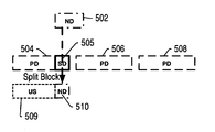
- the abbreviation ‘US’ refers to unused sectors, meaning that the sectors do not contain useful data
- ‘PD’ refers to sectors containing previously written data
- ‘ND’ refers to new data from a host
- ‘SD’ refers to sectors containing stale data, where stale data refers to data targeted to be updated by the (illustrated) re-write operation.
- FIG. 5A shows the start of the operation, beginning with a set of three previously written blocks 504 , 506 , and 508 .
- blocks 504 , 506 , and 508 contain previously written data.
- the external system for example, a personal computer acting as a host
- data to be written to the flash-memory device is represented by new-data 502 .
- physical block 504 contains the first part of the data to be updated, shown as tail portion 505 , which can be overwritten with a head portion of new data 502 .
- the physical blocks containing the contiguous sectors of the rest of the existing data are represented by blocks 506 and 508 .
- Previously written blocks 504 , 506 , and 508 currently represent the physical blocks referenced by address/addresses targeted by the host.
- FMC 200 may begin the re-write operation by acquiring an unused physical block 510 , which is a physical block that contains no data, and generate a ‘split-block’. Alternately, FMC 200 may allocate a new block that contains all stale data, erase the new block since all data contained therein is stale, designate the new block as the unused physical block, and generate a ‘split-block’.
- FMC 200 may write the head portion of new data 502 to the tail section 510 of newly allocated physical block 509 .
- tail section 510 may now correspond to stale data section 505 of physical block 504 .
- This condition/reallocation may be recorded in the split-block record (stored in SRAM 208 , for example) by FMC 200 .
- FMC 200 may next allocate new physical block 520 , and continue writing a second portion of new data 502 to the head section 522 a of physical block 520 .
- the address (targeted by the host) that originally referenced head section 512 a of physical block 506 may now reference head section 522 a of physical block 520 , as also re-allocated by FMC 200 .
- data in head section 512 a of physical block 506 may also be designated as stale by FMC 200 .
- FIG. 5C illustrates a third portion of new data 502 being written to a center section of physical block 520 , shown as section 522 b that also comprises previously written head section 522 a .
- the address (targeted by the host) that originally referenced section 512 b (also comprising previously written head section 512 a ) of physical block 506 may now reference section 522 b of physical block 520 , as also re-allocated by FMC 200 .
- FIG. 5D illustrates a fourth portion of new data 502 being written to the tail section of physical block 520 , shown as section 522 c that also comprises previously written section 522 b .
- the address (targeted by the host) that originally referenced section 512 c (also comprising previously written section 512 b ) of physical block 506 may now reference section 522 c of physical block 520 , as also re-allocated by FMC 200 .
- FIG. 5E illustrates the tail portion of new data 502 being written to the head section 528 of newly allocated physical block 526 .
- the address (targeted by the host) that originally referenced head section 524 of physical block 508 may now reference head section 528 of physical block 526 , as also re-allocated by FMC 200 .
- physical block 506 may be designated as containing all stale data, and may thus be erased and marked as an available physical block for subsequent re-write operations.
- FMC 200 may condense split-blocks following a successful re-write operation, as illustrated in FIGS. 6A through 6C .
- FIG. 6A shows the status of the split-blocks as they appear at the end of a re-write operation, for example the end status of a re-write operation as illustrated in FIG. 5E .
- FMC 200 may write the previously written data sectors of physical blocks 604 and 604 to the unused sectors of physical blocks 610 and 614 , respectively.
- FMC 200 may now designate physical blocks 602 and 604 as being available as candidate blocks for future re-write operations, ending up with physical blocks 610 , 612 , and 614 holding the previously written data and the new data, as shown in FIG. 6C .
- FIG. 7 illustrates how a small file (a file of smaller size than a block) may be written, according to one embodiment.
- FMC 200 may designate new candidate physical block 704 and write the new data to section 708 as shown.
- the address (targeted by the host) that originally referenced section 706 of physical block 702 may now reference section 708 of physical block 704 , as re-allocated by FMC 200 .
- Data in section 706 may be designated as stale by FMC 200 .
- FIGS. 8A-B illustrate how a split-block may be updated when writing a small file, according to one embodiment.
- FMC 200 may access physical block 804 , which already contains a section 808 of previously written data. Again, the address originally targeted by the host may have been referencing section 806 of physical block 802 , but may now be referencing section 808 of physical block 804 , as previously re-allocated by FMC 200 (for example in a write operation as shown in FIG. 7 ). FMC 200 may write new data 810 to physical block 804 , as shown in FIG. 8B .
- FIGS. 9A-D illustrate how resources are reclaimed in one embodiment.
- FIG. 9A shows a split-block comprising physical blocks 604 and 610 , where previously written data in section 612 may represent data that has overwritten the now stale data shown in section 606 .
- FMC 200 may allocate a new block 614 to service a new re-write operation that may be initiated by the host to write new data 602 .
- New data 602 may be written to section 616 of newly allocated physical block 614 , as illustrated in FIG. 9B .
- the new re-write operation results in a portion of new data 602 overwriting a portion of the previously written data shown in section 612 .
- data from physical blocks 610 and 614 may be merged together in physical block 614 , where the non-updated portion of the previously written data in section 612 may be copied to the corresponding sectors 618 in physical block 614 .
- Physical block 610 may then be erased and made available as a potential candidate block for future re-write operations.
- the result may be a single split-block comprising physical blocks 604 and 614 .
- FMC 200 may reclaim resources by copying data from a predecessor block (in this example sectors 612 of physical block 610 ) to a subsequent block (physical block 614 ).
- the predecessor block (physical block 610 ) may then be reclaimed. Note that reclaiming resources at this point may not necessarily be required. It may be preferable to defer the reclamation in case the external system issues a re-write of the data that would otherwise have been merged (the portion of the data in sectors 612 that was copied to sectors 618 ).
Abstract
Description
Claims (32)
Priority Applications (1)
| Application Number | Priority Date | Filing Date | Title |
|---|---|---|---|
| US11/098,707 US7849253B2 (en) | 2005-04-04 | 2005-04-04 | Method for fast access to flash-memory media |
Applications Claiming Priority (1)
| Application Number | Priority Date | Filing Date | Title |
|---|---|---|---|
| US11/098,707 US7849253B2 (en) | 2005-04-04 | 2005-04-04 | Method for fast access to flash-memory media |
Publications (2)
| Publication Number | Publication Date |
|---|---|
| US20060224818A1 US20060224818A1 (en) | 2006-10-05 |
| US7849253B2 true US7849253B2 (en) | 2010-12-07 |
Family
ID=37071970
Family Applications (1)
| Application Number | Title | Priority Date | Filing Date |
|---|---|---|---|
| US11/098,707 Active 2026-08-12 US7849253B2 (en) | 2005-04-04 | 2005-04-04 | Method for fast access to flash-memory media |
Country Status (1)
| Country | Link |
|---|---|
| US (1) | US7849253B2 (en) |
Cited By (8)
| Publication number | Priority date | Publication date | Assignee | Title |
|---|---|---|---|---|
| US20130173842A1 (en) * | 2011-12-28 | 2013-07-04 | King Ying Ng | Adaptive Logical Group Sorting to Prevent Drive Fragmentation |
| US20130219146A1 (en) * | 2012-02-16 | 2013-08-22 | Micron Technology, Inc. | Method, device and system for a configurable address space for non-volatile memory |
| US8521781B2 (en) | 2005-12-22 | 2013-08-27 | Alan Joshua Shapiro | Apparatus and method for selective file erasure using metadata modifications |
| US20150039948A1 (en) * | 2013-07-31 | 2015-02-05 | SK Hynix Inc. | Data storage device and operating method thereof |
| US8990477B2 (en) | 2012-04-19 | 2015-03-24 | Sandisk Technologies Inc. | System and method for limiting fragmentation |
| US10248418B2 (en) | 2015-06-30 | 2019-04-02 | International Business Machines Corporation | Cleared memory indicator |
| US10635308B2 (en) | 2015-06-30 | 2020-04-28 | International Business Machines Corporation | Memory state indicator |
| US10884945B2 (en) | 2015-06-30 | 2021-01-05 | International Business Machines Corporation | Memory state indicator check operations |
Families Citing this family (12)
| Publication number | Priority date | Publication date | Assignee | Title |
|---|---|---|---|---|
| US20060282643A1 (en) * | 2005-06-10 | 2006-12-14 | Subramanyam Chandramouli | Transparent low-density mode for multi-level cell flash memory devices |
| US7984084B2 (en) * | 2005-08-03 | 2011-07-19 | SanDisk Technologies, Inc. | Non-volatile memory with scheduled reclaim operations |
| JP2009503743A (en) | 2005-08-03 | 2009-01-29 | サンディスク コーポレイション | Managing memory blocks that store data files directly |
| WO2007058617A1 (en) * | 2005-11-17 | 2007-05-24 | Chee Keng Chang | A controller for non-volatile memories, and methods of operating the memory controller |
| US8046522B2 (en) * | 2006-12-26 | 2011-10-25 | SanDisk Technologies, Inc. | Use of a direct data file system with a continuous logical address space interface and control of file address storage in logical blocks |
| US8156256B2 (en) * | 2007-04-24 | 2012-04-10 | Samsung Electronics Co., Ltd. | Method for managing logical address and device thereof |
| US8180929B2 (en) * | 2007-04-24 | 2012-05-15 | Samsung Electronics Co., Ltd. | Method for managing logical address and device thereof |
| JP4535117B2 (en) * | 2007-11-06 | 2010-09-01 | ソニー株式会社 | MEMORY DEVICE, MEMORY MANAGEMENT METHOD, AND PROGRAM |
| US7979601B2 (en) * | 2008-08-05 | 2011-07-12 | Standard Microsystems Corporation | External direct memory access of embedded controller memory |
| US9514838B2 (en) * | 2011-05-31 | 2016-12-06 | Micron Technology, Inc. | Apparatus including memory system controllers and related methods for memory management using block tables |
| US10853233B2 (en) * | 2016-10-18 | 2020-12-01 | Toshiba Memory Corporation | Reconstruction of address mapping in a host of a storage system |
| CN116578246B (en) * | 2023-07-05 | 2023-09-29 | 合肥康芯威存储技术有限公司 | Storage device and control method thereof |
Citations (10)
| Publication number | Priority date | Publication date | Assignee | Title |
|---|---|---|---|---|
| US6026465A (en) | 1994-06-03 | 2000-02-15 | Intel Corporation | Flash memory including a mode register for indicating synchronous or asynchronous mode of operation |
| US6505283B1 (en) * | 1998-10-06 | 2003-01-07 | Canon Kabushiki Kaisha | Efficient memory allocator utilizing a dual free-list structure |
| US20030070035A1 (en) * | 2001-10-04 | 2003-04-10 | Chien-Fa Wang | Method for accessing data in a computer and the computer thereof |
| US20030163630A1 (en) * | 2002-02-27 | 2003-08-28 | Aasheim Jered Donald | Dynamic data structures for tracking data stored in a flash memory device |
| US20040057316A1 (en) * | 2002-09-25 | 2004-03-25 | Renesas Technology Corp. | Nonvolatile memory |
| US20050005057A1 (en) * | 2003-07-04 | 2005-01-06 | Chih-Hung Wang | [nonvolatile memory unit with page cache] |
| US6948026B2 (en) * | 2001-08-24 | 2005-09-20 | Micron Technology, Inc. | Erase block management |
| US20060106969A1 (en) * | 2002-12-30 | 2006-05-18 | Koninklijke Philips Electronics N.V. | Memory controller and method for writing to a memory |
| US7139864B2 (en) * | 2003-12-30 | 2006-11-21 | Sandisk Corporation | Non-volatile memory and method with block management system |
| US7340581B2 (en) * | 2001-09-28 | 2008-03-04 | Lexar Media, Inc. | Method of writing data to non-volatile memory |
-
2005
- 2005-04-04 US US11/098,707 patent/US7849253B2/en active Active
Patent Citations (10)
| Publication number | Priority date | Publication date | Assignee | Title |
|---|---|---|---|---|
| US6026465A (en) | 1994-06-03 | 2000-02-15 | Intel Corporation | Flash memory including a mode register for indicating synchronous or asynchronous mode of operation |
| US6505283B1 (en) * | 1998-10-06 | 2003-01-07 | Canon Kabushiki Kaisha | Efficient memory allocator utilizing a dual free-list structure |
| US6948026B2 (en) * | 2001-08-24 | 2005-09-20 | Micron Technology, Inc. | Erase block management |
| US7340581B2 (en) * | 2001-09-28 | 2008-03-04 | Lexar Media, Inc. | Method of writing data to non-volatile memory |
| US20030070035A1 (en) * | 2001-10-04 | 2003-04-10 | Chien-Fa Wang | Method for accessing data in a computer and the computer thereof |
| US20030163630A1 (en) * | 2002-02-27 | 2003-08-28 | Aasheim Jered Donald | Dynamic data structures for tracking data stored in a flash memory device |
| US20040057316A1 (en) * | 2002-09-25 | 2004-03-25 | Renesas Technology Corp. | Nonvolatile memory |
| US20060106969A1 (en) * | 2002-12-30 | 2006-05-18 | Koninklijke Philips Electronics N.V. | Memory controller and method for writing to a memory |
| US20050005057A1 (en) * | 2003-07-04 | 2005-01-06 | Chih-Hung Wang | [nonvolatile memory unit with page cache] |
| US7139864B2 (en) * | 2003-12-30 | 2006-11-21 | Sandisk Corporation | Non-volatile memory and method with block management system |
Non-Patent Citations (4)
| Title |
|---|
| Chiang et al., "Partitioned Log-based Flash Memory management and adaptive cleaning,"International Symposium On Consumer Electronics 2000; Dec. 5-7, 2000, Hong Kong. |
| Design of a solid-state file using flash EEPROM, by H. Niijima; IBM J. Res. Develop. vol. 39 No. 5; Sep. 1995. |
| SCSI-3 Block Commands (SBC), Revision 8c, ANSI NCITS 306-199x; American National Standard for Information Technology; Nov. 13, 1997. |
| SMIL (SmartMedia Interface Library), Software Edition, Version 1.00; Toshiba Corporation; Jul. 1, 2000. |
Cited By (13)
| Publication number | Priority date | Publication date | Assignee | Title |
|---|---|---|---|---|
| US9171005B2 (en) | 2005-12-22 | 2015-10-27 | Alan Joshua Shapiro | System and method for selective file erasure using metadata modifcations |
| US8521781B2 (en) | 2005-12-22 | 2013-08-27 | Alan Joshua Shapiro | Apparatus and method for selective file erasure using metadata modifications |
| US8782089B2 (en) | 2005-12-22 | 2014-07-15 | Alan Joshua Shapiro | Selective file erasure using metadata modifications and apparatus |
| US20130173842A1 (en) * | 2011-12-28 | 2013-07-04 | King Ying Ng | Adaptive Logical Group Sorting to Prevent Drive Fragmentation |
| US20130219146A1 (en) * | 2012-02-16 | 2013-08-22 | Micron Technology, Inc. | Method, device and system for a configurable address space for non-volatile memory |
| US8990477B2 (en) | 2012-04-19 | 2015-03-24 | Sandisk Technologies Inc. | System and method for limiting fragmentation |
| US20150039948A1 (en) * | 2013-07-31 | 2015-02-05 | SK Hynix Inc. | Data storage device and operating method thereof |
| US9372741B2 (en) * | 2013-07-31 | 2016-06-21 | SK Hynix Inc. | Data storage device and operating method thereof |
| US10248418B2 (en) | 2015-06-30 | 2019-04-02 | International Business Machines Corporation | Cleared memory indicator |
| US10635308B2 (en) | 2015-06-30 | 2020-04-28 | International Business Machines Corporation | Memory state indicator |
| US10635307B2 (en) | 2015-06-30 | 2020-04-28 | International Business Machines Corporation | Memory state indicator |
| US10884945B2 (en) | 2015-06-30 | 2021-01-05 | International Business Machines Corporation | Memory state indicator check operations |
| US10884946B2 (en) | 2015-06-30 | 2021-01-05 | International Business Machines Corporation | Memory state indicator check operations |
Also Published As
| Publication number | Publication date |
|---|---|
| US20060224818A1 (en) | 2006-10-05 |
Similar Documents
| Publication | Publication Date | Title |
|---|---|---|
| US7849253B2 (en) | Method for fast access to flash-memory media | |
| US7395384B2 (en) | Method and apparatus for maintaining data on non-volatile memory systems | |
| US8041878B2 (en) | Flash file system | |
| US8122193B2 (en) | Storage device and user device including the same | |
| US7861028B2 (en) | System and method for configuration and management of flash memory | |
| US7752412B2 (en) | Methods of managing file allocation table information | |
| US7840617B2 (en) | Host device and memory system | |
| JP4611024B2 (en) | Method and apparatus for grouping pages in a block | |
| US8838875B2 (en) | Systems, methods and computer program products for operating a data processing system in which a file delete command is sent to an external storage device for invalidating data thereon | |
| JP4766240B2 (en) | File management method, apparatus, and program | |
| CN101484882B (en) | Method for flash-memory management | |
| US7681008B2 (en) | Systems for managing file allocation table information | |
| US7610434B2 (en) | File recording apparatus | |
| US8307172B2 (en) | Memory system including memory controller and separately formatted nonvolatile memory to avoid “copy-involving write” during updating file data in the memory | |
| US20070130442A1 (en) | Apparatus and Methods Using Invalidity Indicators for Buffered Memory | |
| US20080270730A1 (en) | Method for efficient storage of metadata in flash memory | |
| US20060020745A1 (en) | Fat analysis for optimized sequential cluster management | |
| US20110302224A1 (en) | Data storage device with preloaded content | |
| JPWO2007066720A1 (en) | Nonvolatile storage device, data read method, and management table creation method | |
| US7702845B2 (en) | Method and apparatus for managing blocks according to update type of data in block-type memory | |
| KR20070096429A (en) | Fast mounting for a file system on nand flash memory | |
| CN101019098A (en) | File storage device, host apparatus, method for formatting nonvolatile semiconductor memory, and method of writing data in nonvolatile semiconductor memory | |
| JP4157501B2 (en) | Storage device | |
| US7167964B1 (en) | Memory defragmentation in chipcards | |
| EP1046996B1 (en) | Memory defragmentation in chipcards |
Legal Events
| Date | Code | Title | Description |
|---|---|---|---|
| AS | Assignment |
Owner name: STANDARD MICROSYSTEMS CORPORATION, NEW YORK Free format text: ASSIGNMENT OF ASSIGNORS INTEREST;ASSIGNOR:STEWART, GUY A.;REEL/FRAME:016453/0136 Effective date: 20050325 |
|
| STCF | Information on status: patent grant |
Free format text: PATENTED CASE |
|
| FPAY | Fee payment |
Year of fee payment: 4 |
|
| AS | Assignment |
Owner name: MICROCHIP TECHNOLOGY INCORPORATED, ARIZONA Free format text: MERGER;ASSIGNOR:STANDARD MICROSYSTEMS CORPORATION;REEL/FRAME:044824/0608 Effective date: 20120501 |
|
| MAFP | Maintenance fee payment |
Free format text: PAYMENT OF MAINTENANCE FEE, 8TH YEAR, LARGE ENTITY (ORIGINAL EVENT CODE: M1552) Year of fee payment: 8 |
|
| AS | Assignment |
Owner name: JPMORGAN CHASE BANK, N.A., AS ADMINISTRATIVE AGENT, DELAWARE Free format text: SECURITY INTEREST;ASSIGNORS:MICROCHIP TECHNOLOGY INC.;SILICON STORAGE TECHNOLOGY, INC.;ATMEL CORPORATION;AND OTHERS;REEL/FRAME:053311/0305 Effective date: 20200327 |
|
| AS | Assignment |
Owner name: SILICON STORAGE TECHNOLOGY, INC., ARIZONA Free format text: RELEASE BY SECURED PARTY;ASSIGNOR:JPMORGAN CHASE BANK, N.A, AS ADMINISTRATIVE AGENT;REEL/FRAME:053466/0011 Effective date: 20200529 Owner name: MICROCHIP TECHNOLOGY INC., ARIZONA Free format text: RELEASE BY SECURED PARTY;ASSIGNOR:JPMORGAN CHASE BANK, N.A, AS ADMINISTRATIVE AGENT;REEL/FRAME:053466/0011 Effective date: 20200529 Owner name: ATMEL CORPORATION, ARIZONA Free format text: RELEASE BY SECURED PARTY;ASSIGNOR:JPMORGAN CHASE BANK, N.A, AS ADMINISTRATIVE AGENT;REEL/FRAME:053466/0011 Effective date: 20200529 Owner name: MICROSEMI CORPORATION, CALIFORNIA Free format text: RELEASE BY SECURED PARTY;ASSIGNOR:JPMORGAN CHASE BANK, N.A, AS ADMINISTRATIVE AGENT;REEL/FRAME:053466/0011 Effective date: 20200529 Owner name: MICROSEMI STORAGE SOLUTIONS, INC., ARIZONA Free format text: RELEASE BY SECURED PARTY;ASSIGNOR:JPMORGAN CHASE BANK, N.A, AS ADMINISTRATIVE AGENT;REEL/FRAME:053466/0011 Effective date: 20200529 |
|
| AS | Assignment |
Owner name: WELLS FARGO BANK, NATIONAL ASSOCIATION, MINNESOTA Free format text: SECURITY INTEREST;ASSIGNORS:MICROCHIP TECHNOLOGY INC.;SILICON STORAGE TECHNOLOGY, INC.;ATMEL CORPORATION;AND OTHERS;REEL/FRAME:053468/0705 Effective date: 20200529 |
|
| AS | Assignment |
Owner name: WELLS FARGO BANK, NATIONAL ASSOCIATION, AS COLLATERAL AGENT, MINNESOTA Free format text: SECURITY INTEREST;ASSIGNORS:MICROCHIP TECHNOLOGY INCORPORATED;SILICON STORAGE TECHNOLOGY, INC.;ATMEL CORPORATION;AND OTHERS;REEL/FRAME:055671/0612 Effective date: 20201217 |
|
| AS | Assignment |
Owner name: WELLS FARGO BANK, NATIONAL ASSOCIATION, AS NOTES COLLATERAL AGENT, MINNESOTA Free format text: SECURITY INTEREST;ASSIGNORS:MICROCHIP TECHNOLOGY INCORPORATED;SILICON STORAGE TECHNOLOGY, INC.;ATMEL CORPORATION;AND OTHERS;REEL/FRAME:057935/0474 Effective date: 20210528 |
|
| AS | Assignment |
Owner name: MICROSEMI STORAGE SOLUTIONS, INC., ARIZONA Free format text: RELEASE BY SECURED PARTY;ASSIGNOR:WELLS FARGO BANK, NATIONAL ASSOCIATION, AS NOTES COLLATERAL AGENT;REEL/FRAME:059863/0400 Effective date: 20220228 Owner name: MICROSEMI CORPORATION, ARIZONA Free format text: RELEASE BY SECURED PARTY;ASSIGNOR:WELLS FARGO BANK, NATIONAL ASSOCIATION, AS NOTES COLLATERAL AGENT;REEL/FRAME:059863/0400 Effective date: 20220228 Owner name: ATMEL CORPORATION, ARIZONA Free format text: RELEASE BY SECURED PARTY;ASSIGNOR:WELLS FARGO BANK, NATIONAL ASSOCIATION, AS NOTES COLLATERAL AGENT;REEL/FRAME:059863/0400 Effective date: 20220228 Owner name: SILICON STORAGE TECHNOLOGY, INC., ARIZONA Free format text: RELEASE BY SECURED PARTY;ASSIGNOR:WELLS FARGO BANK, NATIONAL ASSOCIATION, AS NOTES COLLATERAL AGENT;REEL/FRAME:059863/0400 Effective date: 20220228 Owner name: MICROCHIP TECHNOLOGY INCORPORATED, ARIZONA Free format text: RELEASE BY SECURED PARTY;ASSIGNOR:WELLS FARGO BANK, NATIONAL ASSOCIATION, AS NOTES COLLATERAL AGENT;REEL/FRAME:059863/0400 Effective date: 20220228 |
|
| AS | Assignment |
Owner name: MICROSEMI STORAGE SOLUTIONS, INC., ARIZONA Free format text: RELEASE BY SECURED PARTY;ASSIGNOR:WELLS FARGO BANK, NATIONAL ASSOCIATION, AS NOTES COLLATERAL AGENT;REEL/FRAME:059363/0001 Effective date: 20220228 Owner name: MICROSEMI CORPORATION, ARIZONA Free format text: RELEASE BY SECURED PARTY;ASSIGNOR:WELLS FARGO BANK, NATIONAL ASSOCIATION, AS NOTES COLLATERAL AGENT;REEL/FRAME:059363/0001 Effective date: 20220228 Owner name: ATMEL CORPORATION, ARIZONA Free format text: RELEASE BY SECURED PARTY;ASSIGNOR:WELLS FARGO BANK, NATIONAL ASSOCIATION, AS NOTES COLLATERAL AGENT;REEL/FRAME:059363/0001 Effective date: 20220228 Owner name: SILICON STORAGE TECHNOLOGY, INC., ARIZONA Free format text: RELEASE BY SECURED PARTY;ASSIGNOR:WELLS FARGO BANK, NATIONAL ASSOCIATION, AS NOTES COLLATERAL AGENT;REEL/FRAME:059363/0001 Effective date: 20220228 Owner name: MICROCHIP TECHNOLOGY INCORPORATED, ARIZONA Free format text: RELEASE BY SECURED PARTY;ASSIGNOR:WELLS FARGO BANK, NATIONAL ASSOCIATION, AS NOTES COLLATERAL AGENT;REEL/FRAME:059363/0001 Effective date: 20220228 |
|
| AS | Assignment |
Owner name: MICROSEMI STORAGE SOLUTIONS, INC., ARIZONA Free format text: RELEASE BY SECURED PARTY;ASSIGNOR:WELLS FARGO BANK, NATIONAL ASSOCIATION, AS NOTES COLLATERAL AGENT;REEL/FRAME:060894/0437 Effective date: 20220228 Owner name: MICROSEMI CORPORATION, ARIZONA Free format text: RELEASE BY SECURED PARTY;ASSIGNOR:WELLS FARGO BANK, NATIONAL ASSOCIATION, AS NOTES COLLATERAL AGENT;REEL/FRAME:060894/0437 Effective date: 20220228 Owner name: ATMEL CORPORATION, ARIZONA Free format text: RELEASE BY SECURED PARTY;ASSIGNOR:WELLS FARGO BANK, NATIONAL ASSOCIATION, AS NOTES COLLATERAL AGENT;REEL/FRAME:060894/0437 Effective date: 20220228 Owner name: SILICON STORAGE TECHNOLOGY, INC., ARIZONA Free format text: RELEASE BY SECURED PARTY;ASSIGNOR:WELLS FARGO BANK, NATIONAL ASSOCIATION, AS NOTES COLLATERAL AGENT;REEL/FRAME:060894/0437 Effective date: 20220228 Owner name: MICROCHIP TECHNOLOGY INCORPORATED, ARIZONA Free format text: RELEASE BY SECURED PARTY;ASSIGNOR:WELLS FARGO BANK, NATIONAL ASSOCIATION, AS NOTES COLLATERAL AGENT;REEL/FRAME:060894/0437 Effective date: 20220228 |
|
| MAFP | Maintenance fee payment |
Free format text: PAYMENT OF MAINTENANCE FEE, 12TH YEAR, LARGE ENTITY (ORIGINAL EVENT CODE: M1553); ENTITY STATUS OF PATENT OWNER: LARGE ENTITY Year of fee payment: 12 |