US7868446B2 - Semiconductor device and methods of manufacturing semiconductor devices - Google Patents
Semiconductor device and methods of manufacturing semiconductor devices Download PDFInfo
- Publication number
- US7868446B2 US7868446B2 US11/850,750 US85075007A US7868446B2 US 7868446 B2 US7868446 B2 US 7868446B2 US 85075007 A US85075007 A US 85075007A US 7868446 B2 US7868446 B2 US 7868446B2
- Authority
- US
- United States
- Prior art keywords
- molded body
- semiconductor device
- elements
- elastic
- elastic elements
- Prior art date
- Legal status (The legal status is an assumption and is not a legal conclusion. Google has not performed a legal analysis and makes no representation as to the accuracy of the status listed.)
- Expired - Fee Related, expires
Links
Images


Classifications
-
- H—ELECTRICITY
- H01—ELECTRIC ELEMENTS
- H01L—SEMICONDUCTOR DEVICES NOT COVERED BY CLASS H10
- H01L23/00—Details of semiconductor or other solid state devices
- H01L23/28—Encapsulations, e.g. encapsulating layers, coatings, e.g. for protection
-
- H—ELECTRICITY
- H01—ELECTRIC ELEMENTS
- H01L—SEMICONDUCTOR DEVICES NOT COVERED BY CLASS H10
- H01L24/00—Arrangements for connecting or disconnecting semiconductor or solid-state bodies; Methods or apparatus related thereto
- H01L24/93—Batch processes
- H01L24/95—Batch processes at chip-level, i.e. with connecting carried out on a plurality of singulated devices, i.e. on diced chips
- H01L24/96—Batch processes at chip-level, i.e. with connecting carried out on a plurality of singulated devices, i.e. on diced chips the devices being encapsulated in a common layer, e.g. neo-wafer or pseudo-wafer, said common layer being separable into individual assemblies after connecting
-
- H—ELECTRICITY
- H01—ELECTRIC ELEMENTS
- H01L—SEMICONDUCTOR DEVICES NOT COVERED BY CLASS H10
- H01L21/00—Processes or apparatus adapted for the manufacture or treatment of semiconductor or solid state devices or of parts thereof
- H01L21/02—Manufacture or treatment of semiconductor devices or of parts thereof
- H01L21/04—Manufacture or treatment of semiconductor devices or of parts thereof the devices having at least one potential-jump barrier or surface barrier, e.g. PN junction, depletion layer or carrier concentration layer
- H01L21/50—Assembly of semiconductor devices using processes or apparatus not provided for in a single one of the subgroups H01L21/06 - H01L21/326, e.g. sealing of a cap to a base of a container
- H01L21/56—Encapsulations, e.g. encapsulation layers, coatings
- H01L21/561—Batch processing
-
- H—ELECTRICITY
- H01—ELECTRIC ELEMENTS
- H01L—SEMICONDUCTOR DEVICES NOT COVERED BY CLASS H10
- H01L21/00—Processes or apparatus adapted for the manufacture or treatment of semiconductor or solid state devices or of parts thereof
- H01L21/02—Manufacture or treatment of semiconductor devices or of parts thereof
- H01L21/04—Manufacture or treatment of semiconductor devices or of parts thereof the devices having at least one potential-jump barrier or surface barrier, e.g. PN junction, depletion layer or carrier concentration layer
- H01L21/50—Assembly of semiconductor devices using processes or apparatus not provided for in a single one of the subgroups H01L21/06 - H01L21/326, e.g. sealing of a cap to a base of a container
- H01L21/56—Encapsulations, e.g. encapsulation layers, coatings
- H01L21/568—Temporary substrate used as encapsulation process aid
-
- H—ELECTRICITY
- H01—ELECTRIC ELEMENTS
- H01L—SEMICONDUCTOR DEVICES NOT COVERED BY CLASS H10
- H01L21/00—Processes or apparatus adapted for the manufacture or treatment of semiconductor or solid state devices or of parts thereof
- H01L21/67—Apparatus specially adapted for handling semiconductor or electric solid state devices during manufacture or treatment thereof; Apparatus specially adapted for handling wafers during manufacture or treatment of semiconductor or electric solid state devices or components ; Apparatus not specifically provided for elsewhere
- H01L21/683—Apparatus specially adapted for handling semiconductor or electric solid state devices during manufacture or treatment thereof; Apparatus specially adapted for handling wafers during manufacture or treatment of semiconductor or electric solid state devices or components ; Apparatus not specifically provided for elsewhere for supporting or gripping
- H01L21/6835—Apparatus specially adapted for handling semiconductor or electric solid state devices during manufacture or treatment thereof; Apparatus specially adapted for handling wafers during manufacture or treatment of semiconductor or electric solid state devices or components ; Apparatus not specifically provided for elsewhere for supporting or gripping using temporarily an auxiliary support
-
- H—ELECTRICITY
- H01—ELECTRIC ELEMENTS
- H01L—SEMICONDUCTOR DEVICES NOT COVERED BY CLASS H10
- H01L23/00—Details of semiconductor or other solid state devices
- H01L23/16—Fillings or auxiliary members in containers or encapsulations, e.g. centering rings
-
- H—ELECTRICITY
- H01—ELECTRIC ELEMENTS
- H01L—SEMICONDUCTOR DEVICES NOT COVERED BY CLASS H10
- H01L23/00—Details of semiconductor or other solid state devices
- H01L23/28—Encapsulations, e.g. encapsulating layers, coatings, e.g. for protection
- H01L23/31—Encapsulations, e.g. encapsulating layers, coatings, e.g. for protection characterised by the arrangement or shape
- H01L23/3107—Encapsulations, e.g. encapsulating layers, coatings, e.g. for protection characterised by the arrangement or shape the device being completely enclosed
- H01L23/3121—Encapsulations, e.g. encapsulating layers, coatings, e.g. for protection characterised by the arrangement or shape the device being completely enclosed a substrate forming part of the encapsulation
- H01L23/3128—Encapsulations, e.g. encapsulating layers, coatings, e.g. for protection characterised by the arrangement or shape the device being completely enclosed a substrate forming part of the encapsulation the substrate having spherical bumps for external connection
-
- H—ELECTRICITY
- H01—ELECTRIC ELEMENTS
- H01L—SEMICONDUCTOR DEVICES NOT COVERED BY CLASS H10
- H01L23/00—Details of semiconductor or other solid state devices
- H01L23/28—Encapsulations, e.g. encapsulating layers, coatings, e.g. for protection
- H01L23/31—Encapsulations, e.g. encapsulating layers, coatings, e.g. for protection characterised by the arrangement or shape
- H01L23/3107—Encapsulations, e.g. encapsulating layers, coatings, e.g. for protection characterised by the arrangement or shape the device being completely enclosed
- H01L23/3142—Sealing arrangements between parts, e.g. adhesion promotors
-
- H—ELECTRICITY
- H01—ELECTRIC ELEMENTS
- H01L—SEMICONDUCTOR DEVICES NOT COVERED BY CLASS H10
- H01L23/00—Details of semiconductor or other solid state devices
- H01L23/562—Protection against mechanical damage
-
- H—ELECTRICITY
- H01—ELECTRIC ELEMENTS
- H01L—SEMICONDUCTOR DEVICES NOT COVERED BY CLASS H10
- H01L24/00—Arrangements for connecting or disconnecting semiconductor or solid-state bodies; Methods or apparatus related thereto
- H01L24/01—Means for bonding being attached to, or being formed on, the surface to be connected, e.g. chip-to-package, die-attach, "first-level" interconnects; Manufacturing methods related thereto
- H01L24/02—Bonding areas ; Manufacturing methods related thereto
-
- H—ELECTRICITY
- H01—ELECTRIC ELEMENTS
- H01L—SEMICONDUCTOR DEVICES NOT COVERED BY CLASS H10
- H01L24/00—Arrangements for connecting or disconnecting semiconductor or solid-state bodies; Methods or apparatus related thereto
- H01L24/93—Batch processes
- H01L24/95—Batch processes at chip-level, i.e. with connecting carried out on a plurality of singulated devices, i.e. on diced chips
- H01L24/97—Batch processes at chip-level, i.e. with connecting carried out on a plurality of singulated devices, i.e. on diced chips the devices being connected to a common substrate, e.g. interposer, said common substrate being separable into individual assemblies after connecting
-
- H—ELECTRICITY
- H01—ELECTRIC ELEMENTS
- H01L—SEMICONDUCTOR DEVICES NOT COVERED BY CLASS H10
- H01L2224/00—Indexing scheme for arrangements for connecting or disconnecting semiconductor or solid-state bodies and methods related thereto as covered by H01L24/00
- H01L2224/01—Means for bonding being attached to, or being formed on, the surface to be connected, e.g. chip-to-package, die-attach, "first-level" interconnects; Manufacturing methods related thereto
- H01L2224/02—Bonding areas; Manufacturing methods related thereto
- H01L2224/023—Redistribution layers [RDL] for bonding areas
- H01L2224/0231—Manufacturing methods of the redistribution layers
-
- H—ELECTRICITY
- H01—ELECTRIC ELEMENTS
- H01L—SEMICONDUCTOR DEVICES NOT COVERED BY CLASS H10
- H01L2224/00—Indexing scheme for arrangements for connecting or disconnecting semiconductor or solid-state bodies and methods related thereto as covered by H01L24/00
- H01L2224/01—Means for bonding being attached to, or being formed on, the surface to be connected, e.g. chip-to-package, die-attach, "first-level" interconnects; Manufacturing methods related thereto
- H01L2224/02—Bonding areas; Manufacturing methods related thereto
- H01L2224/023—Redistribution layers [RDL] for bonding areas
- H01L2224/0237—Disposition of the redistribution layers
- H01L2224/02379—Fan-out arrangement
-
- H—ELECTRICITY
- H01—ELECTRIC ELEMENTS
- H01L—SEMICONDUCTOR DEVICES NOT COVERED BY CLASS H10
- H01L2224/00—Indexing scheme for arrangements for connecting or disconnecting semiconductor or solid-state bodies and methods related thereto as covered by H01L24/00
- H01L2224/01—Means for bonding being attached to, or being formed on, the surface to be connected, e.g. chip-to-package, die-attach, "first-level" interconnects; Manufacturing methods related thereto
- H01L2224/02—Bonding areas; Manufacturing methods related thereto
- H01L2224/04—Structure, shape, material or disposition of the bonding areas prior to the connecting process
- H01L2224/04105—Bonding areas formed on an encapsulation of the semiconductor or solid-state body, e.g. bonding areas on chip-scale packages
-
- H—ELECTRICITY
- H01—ELECTRIC ELEMENTS
- H01L—SEMICONDUCTOR DEVICES NOT COVERED BY CLASS H10
- H01L2224/00—Indexing scheme for arrangements for connecting or disconnecting semiconductor or solid-state bodies and methods related thereto as covered by H01L24/00
- H01L2224/01—Means for bonding being attached to, or being formed on, the surface to be connected, e.g. chip-to-package, die-attach, "first-level" interconnects; Manufacturing methods related thereto
- H01L2224/02—Bonding areas; Manufacturing methods related thereto
- H01L2224/04—Structure, shape, material or disposition of the bonding areas prior to the connecting process
- H01L2224/05—Structure, shape, material or disposition of the bonding areas prior to the connecting process of an individual bonding area
- H01L2224/05001—Internal layers
- H01L2224/0502—Disposition
- H01L2224/05024—Disposition the internal layer being disposed on a redistribution layer on the semiconductor or solid-state body
-
- H—ELECTRICITY
- H01—ELECTRIC ELEMENTS
- H01L—SEMICONDUCTOR DEVICES NOT COVERED BY CLASS H10
- H01L2224/00—Indexing scheme for arrangements for connecting or disconnecting semiconductor or solid-state bodies and methods related thereto as covered by H01L24/00
- H01L2224/01—Means for bonding being attached to, or being formed on, the surface to be connected, e.g. chip-to-package, die-attach, "first-level" interconnects; Manufacturing methods related thereto
- H01L2224/02—Bonding areas; Manufacturing methods related thereto
- H01L2224/04—Structure, shape, material or disposition of the bonding areas prior to the connecting process
- H01L2224/05—Structure, shape, material or disposition of the bonding areas prior to the connecting process of an individual bonding area
- H01L2224/05001—Internal layers
- H01L2224/0502—Disposition
- H01L2224/05026—Disposition the internal layer being disposed in a recess of the surface
-
- H—ELECTRICITY
- H01—ELECTRIC ELEMENTS
- H01L—SEMICONDUCTOR DEVICES NOT COVERED BY CLASS H10
- H01L2224/00—Indexing scheme for arrangements for connecting or disconnecting semiconductor or solid-state bodies and methods related thereto as covered by H01L24/00
- H01L2224/01—Means for bonding being attached to, or being formed on, the surface to be connected, e.g. chip-to-package, die-attach, "first-level" interconnects; Manufacturing methods related thereto
- H01L2224/02—Bonding areas; Manufacturing methods related thereto
- H01L2224/04—Structure, shape, material or disposition of the bonding areas prior to the connecting process
- H01L2224/05—Structure, shape, material or disposition of the bonding areas prior to the connecting process of an individual bonding area
- H01L2224/0554—External layer
- H01L2224/05541—Structure
- H01L2224/05548—Bonding area integrally formed with a redistribution layer on the semiconductor or solid-state body
-
- H—ELECTRICITY
- H01—ELECTRIC ELEMENTS
- H01L—SEMICONDUCTOR DEVICES NOT COVERED BY CLASS H10
- H01L2224/00—Indexing scheme for arrangements for connecting or disconnecting semiconductor or solid-state bodies and methods related thereto as covered by H01L24/00
- H01L2224/01—Means for bonding being attached to, or being formed on, the surface to be connected, e.g. chip-to-package, die-attach, "first-level" interconnects; Manufacturing methods related thereto
- H01L2224/02—Bonding areas; Manufacturing methods related thereto
- H01L2224/04—Structure, shape, material or disposition of the bonding areas prior to the connecting process
- H01L2224/05—Structure, shape, material or disposition of the bonding areas prior to the connecting process of an individual bonding area
- H01L2224/0554—External layer
- H01L2224/05599—Material
- H01L2224/056—Material with a principal constituent of the material being a metal or a metalloid, e.g. boron [B], silicon [Si], germanium [Ge], arsenic [As], antimony [Sb], tellurium [Te] and polonium [Po], and alloys thereof
- H01L2224/05617—Material with a principal constituent of the material being a metal or a metalloid, e.g. boron [B], silicon [Si], germanium [Ge], arsenic [As], antimony [Sb], tellurium [Te] and polonium [Po], and alloys thereof the principal constituent melting at a temperature of greater than or equal to 400°C and less than 950°C
- H01L2224/05624—Aluminium [Al] as principal constituent
-
- H—ELECTRICITY
- H01—ELECTRIC ELEMENTS
- H01L—SEMICONDUCTOR DEVICES NOT COVERED BY CLASS H10
- H01L2224/00—Indexing scheme for arrangements for connecting or disconnecting semiconductor or solid-state bodies and methods related thereto as covered by H01L24/00
- H01L2224/01—Means for bonding being attached to, or being formed on, the surface to be connected, e.g. chip-to-package, die-attach, "first-level" interconnects; Manufacturing methods related thereto
- H01L2224/02—Bonding areas; Manufacturing methods related thereto
- H01L2224/04—Structure, shape, material or disposition of the bonding areas prior to the connecting process
- H01L2224/06—Structure, shape, material or disposition of the bonding areas prior to the connecting process of a plurality of bonding areas
- H01L2224/061—Disposition
- H01L2224/0612—Layout
- H01L2224/0613—Square or rectangular array
- H01L2224/06134—Square or rectangular array covering only portions of the surface to be connected
- H01L2224/06135—Covering only the peripheral area of the surface to be connected, i.e. peripheral arrangements
-
- H—ELECTRICITY
- H01—ELECTRIC ELEMENTS
- H01L—SEMICONDUCTOR DEVICES NOT COVERED BY CLASS H10
- H01L2224/00—Indexing scheme for arrangements for connecting or disconnecting semiconductor or solid-state bodies and methods related thereto as covered by H01L24/00
- H01L2224/01—Means for bonding being attached to, or being formed on, the surface to be connected, e.g. chip-to-package, die-attach, "first-level" interconnects; Manufacturing methods related thereto
- H01L2224/10—Bump connectors; Manufacturing methods related thereto
- H01L2224/12—Structure, shape, material or disposition of the bump connectors prior to the connecting process
- H01L2224/12105—Bump connectors formed on an encapsulation of the semiconductor or solid-state body, e.g. bumps on chip-scale packages
-
- H—ELECTRICITY
- H01—ELECTRIC ELEMENTS
- H01L—SEMICONDUCTOR DEVICES NOT COVERED BY CLASS H10
- H01L2224/00—Indexing scheme for arrangements for connecting or disconnecting semiconductor or solid-state bodies and methods related thereto as covered by H01L24/00
- H01L2224/93—Batch processes
- H01L2224/95—Batch processes at chip-level, i.e. with connecting carried out on a plurality of singulated devices, i.e. on diced chips
- H01L2224/97—Batch processes at chip-level, i.e. with connecting carried out on a plurality of singulated devices, i.e. on diced chips the devices being connected to a common substrate, e.g. interposer, said common substrate being separable into individual assemblies after connecting
-
- H—ELECTRICITY
- H01—ELECTRIC ELEMENTS
- H01L—SEMICONDUCTOR DEVICES NOT COVERED BY CLASS H10
- H01L24/00—Arrangements for connecting or disconnecting semiconductor or solid-state bodies; Methods or apparatus related thereto
- H01L24/01—Means for bonding being attached to, or being formed on, the surface to be connected, e.g. chip-to-package, die-attach, "first-level" interconnects; Manufacturing methods related thereto
- H01L24/02—Bonding areas ; Manufacturing methods related thereto
- H01L24/03—Manufacturing methods
-
- H—ELECTRICITY
- H01—ELECTRIC ELEMENTS
- H01L—SEMICONDUCTOR DEVICES NOT COVERED BY CLASS H10
- H01L24/00—Arrangements for connecting or disconnecting semiconductor or solid-state bodies; Methods or apparatus related thereto
- H01L24/01—Means for bonding being attached to, or being formed on, the surface to be connected, e.g. chip-to-package, die-attach, "first-level" interconnects; Manufacturing methods related thereto
- H01L24/02—Bonding areas ; Manufacturing methods related thereto
- H01L24/04—Structure, shape, material or disposition of the bonding areas prior to the connecting process
- H01L24/05—Structure, shape, material or disposition of the bonding areas prior to the connecting process of an individual bonding area
-
- H—ELECTRICITY
- H01—ELECTRIC ELEMENTS
- H01L—SEMICONDUCTOR DEVICES NOT COVERED BY CLASS H10
- H01L24/00—Arrangements for connecting or disconnecting semiconductor or solid-state bodies; Methods or apparatus related thereto
- H01L24/01—Means for bonding being attached to, or being formed on, the surface to be connected, e.g. chip-to-package, die-attach, "first-level" interconnects; Manufacturing methods related thereto
- H01L24/02—Bonding areas ; Manufacturing methods related thereto
- H01L24/04—Structure, shape, material or disposition of the bonding areas prior to the connecting process
- H01L24/06—Structure, shape, material or disposition of the bonding areas prior to the connecting process of a plurality of bonding areas
-
- H—ELECTRICITY
- H01—ELECTRIC ELEMENTS
- H01L—SEMICONDUCTOR DEVICES NOT COVERED BY CLASS H10
- H01L24/00—Arrangements for connecting or disconnecting semiconductor or solid-state bodies; Methods or apparatus related thereto
- H01L24/01—Means for bonding being attached to, or being formed on, the surface to be connected, e.g. chip-to-package, die-attach, "first-level" interconnects; Manufacturing methods related thereto
- H01L24/10—Bump connectors ; Manufacturing methods related thereto
- H01L24/12—Structure, shape, material or disposition of the bump connectors prior to the connecting process
- H01L24/13—Structure, shape, material or disposition of the bump connectors prior to the connecting process of an individual bump connector
-
- H—ELECTRICITY
- H01—ELECTRIC ELEMENTS
- H01L—SEMICONDUCTOR DEVICES NOT COVERED BY CLASS H10
- H01L2924/00—Indexing scheme for arrangements or methods for connecting or disconnecting semiconductor or solid-state bodies as covered by H01L24/00
- H01L2924/0001—Technical content checked by a classifier
- H01L2924/00014—Technical content checked by a classifier the subject-matter covered by the group, the symbol of which is combined with the symbol of this group, being disclosed without further technical details
-
- H—ELECTRICITY
- H01—ELECTRIC ELEMENTS
- H01L—SEMICONDUCTOR DEVICES NOT COVERED BY CLASS H10
- H01L2924/00—Indexing scheme for arrangements or methods for connecting or disconnecting semiconductor or solid-state bodies as covered by H01L24/00
- H01L2924/01—Chemical elements
- H01L2924/01005—Boron [B]
-
- H—ELECTRICITY
- H01—ELECTRIC ELEMENTS
- H01L—SEMICONDUCTOR DEVICES NOT COVERED BY CLASS H10
- H01L2924/00—Indexing scheme for arrangements or methods for connecting or disconnecting semiconductor or solid-state bodies as covered by H01L24/00
- H01L2924/01—Chemical elements
- H01L2924/01006—Carbon [C]
-
- H—ELECTRICITY
- H01—ELECTRIC ELEMENTS
- H01L—SEMICONDUCTOR DEVICES NOT COVERED BY CLASS H10
- H01L2924/00—Indexing scheme for arrangements or methods for connecting or disconnecting semiconductor or solid-state bodies as covered by H01L24/00
- H01L2924/01—Chemical elements
- H01L2924/01013—Aluminum [Al]
-
- H—ELECTRICITY
- H01—ELECTRIC ELEMENTS
- H01L—SEMICONDUCTOR DEVICES NOT COVERED BY CLASS H10
- H01L2924/00—Indexing scheme for arrangements or methods for connecting or disconnecting semiconductor or solid-state bodies as covered by H01L24/00
- H01L2924/01—Chemical elements
- H01L2924/01019—Potassium [K]
-
- H—ELECTRICITY
- H01—ELECTRIC ELEMENTS
- H01L—SEMICONDUCTOR DEVICES NOT COVERED BY CLASS H10
- H01L2924/00—Indexing scheme for arrangements or methods for connecting or disconnecting semiconductor or solid-state bodies as covered by H01L24/00
- H01L2924/01—Chemical elements
- H01L2924/01029—Copper [Cu]
-
- H—ELECTRICITY
- H01—ELECTRIC ELEMENTS
- H01L—SEMICONDUCTOR DEVICES NOT COVERED BY CLASS H10
- H01L2924/00—Indexing scheme for arrangements or methods for connecting or disconnecting semiconductor or solid-state bodies as covered by H01L24/00
- H01L2924/01—Chemical elements
- H01L2924/01033—Arsenic [As]
-
- H—ELECTRICITY
- H01—ELECTRIC ELEMENTS
- H01L—SEMICONDUCTOR DEVICES NOT COVERED BY CLASS H10
- H01L2924/00—Indexing scheme for arrangements or methods for connecting or disconnecting semiconductor or solid-state bodies as covered by H01L24/00
- H01L2924/01—Chemical elements
- H01L2924/01046—Palladium [Pd]
-
- H—ELECTRICITY
- H01—ELECTRIC ELEMENTS
- H01L—SEMICONDUCTOR DEVICES NOT COVERED BY CLASS H10
- H01L2924/00—Indexing scheme for arrangements or methods for connecting or disconnecting semiconductor or solid-state bodies as covered by H01L24/00
- H01L2924/01—Chemical elements
- H01L2924/01068—Erbium [Er]
-
- H—ELECTRICITY
- H01—ELECTRIC ELEMENTS
- H01L—SEMICONDUCTOR DEVICES NOT COVERED BY CLASS H10
- H01L2924/00—Indexing scheme for arrangements or methods for connecting or disconnecting semiconductor or solid-state bodies as covered by H01L24/00
- H01L2924/01—Chemical elements
- H01L2924/01079—Gold [Au]
-
- H—ELECTRICITY
- H01—ELECTRIC ELEMENTS
- H01L—SEMICONDUCTOR DEVICES NOT COVERED BY CLASS H10
- H01L2924/00—Indexing scheme for arrangements or methods for connecting or disconnecting semiconductor or solid-state bodies as covered by H01L24/00
- H01L2924/01—Chemical elements
- H01L2924/01082—Lead [Pb]
-
- H—ELECTRICITY
- H01—ELECTRIC ELEMENTS
- H01L—SEMICONDUCTOR DEVICES NOT COVERED BY CLASS H10
- H01L2924/00—Indexing scheme for arrangements or methods for connecting or disconnecting semiconductor or solid-state bodies as covered by H01L24/00
- H01L2924/10—Details of semiconductor or other solid state devices to be connected
- H01L2924/11—Device type
- H01L2924/12—Passive devices, e.g. 2 terminal devices
- H01L2924/1204—Optical Diode
- H01L2924/12044—OLED
-
- H—ELECTRICITY
- H01—ELECTRIC ELEMENTS
- H01L—SEMICONDUCTOR DEVICES NOT COVERED BY CLASS H10
- H01L2924/00—Indexing scheme for arrangements or methods for connecting or disconnecting semiconductor or solid-state bodies as covered by H01L24/00
- H01L2924/10—Details of semiconductor or other solid state devices to be connected
- H01L2924/11—Device type
- H01L2924/14—Integrated circuits
-
- H—ELECTRICITY
- H01—ELECTRIC ELEMENTS
- H01L—SEMICONDUCTOR DEVICES NOT COVERED BY CLASS H10
- H01L2924/00—Indexing scheme for arrangements or methods for connecting or disconnecting semiconductor or solid-state bodies as covered by H01L24/00
- H01L2924/10—Details of semiconductor or other solid state devices to be connected
- H01L2924/146—Mixed devices
- H01L2924/1461—MEMS
-
- H—ELECTRICITY
- H01—ELECTRIC ELEMENTS
- H01L—SEMICONDUCTOR DEVICES NOT COVERED BY CLASS H10
- H01L2924/00—Indexing scheme for arrangements or methods for connecting or disconnecting semiconductor or solid-state bodies as covered by H01L24/00
- H01L2924/15—Details of package parts other than the semiconductor or other solid state devices to be connected
- H01L2924/151—Die mounting substrate
- H01L2924/153—Connection portion
- H01L2924/1531—Connection portion the connection portion being formed only on the surface of the substrate opposite to the die mounting surface
- H01L2924/15311—Connection portion the connection portion being formed only on the surface of the substrate opposite to the die mounting surface being a ball array, e.g. BGA
-
- H—ELECTRICITY
- H01—ELECTRIC ELEMENTS
- H01L—SEMICONDUCTOR DEVICES NOT COVERED BY CLASS H10
- H01L2924/00—Indexing scheme for arrangements or methods for connecting or disconnecting semiconductor or solid-state bodies as covered by H01L24/00
- H01L2924/15—Details of package parts other than the semiconductor or other solid state devices to be connected
- H01L2924/181—Encapsulation
Definitions
- the present invention relates to a semiconductor device and methods of manufacturing semiconductor devices.
- BGA Ball Grid Array
- a semiconductor device comprising a semiconductor chip; a molded body covering the semiconductor chip, the molded body comprising an array of recesses in a first surface of the molded body; first contact elements; and elastic elements in the recesses that connect the first contact elements with the molded body.
- FIGS. 1A and 1B schematically disclose two views of cross sections of a semiconductor device soldered to a printed circuit board along the axes 1 A- 1 A′ and 1 B- 1 B′;
- FIGS. 2A and 2B schematically disclose two orthogonal cross sections of an embodiment with first contact elements and elastic elements that connect the first contact elements with a molded body housing a semiconductor chip;
- FIG. 3 schematically discloses an orthogonal cross section of a further embodiment with first contact elements and with elastic elements that connect the first contact elements with a molded body housing a semiconductor chip, whereby the elastic elements are flush with a first surface of the molded body;
- FIG. 4 schematically discloses a cross section of a further embodiment like in FIG. 3 with the difference that the elastic elements are mechanically interlocked with the recesses;
- FIGS. 5A and 5B schematically discloses views of two orthogonal cross sections of a further embodiment disclosing conducting lines that electrically connect the first contact elements with the semiconductor chip;
- FIGS. 6A and 6B schematically disclose a further embodiment wherein the semiconductor chip comprises first contact elements that are connected to the molded body by means of elastic elements, and second contact elements that are rigidly connected to the semiconductor chip;
- FIGS. 7A to 7H schematically disclose an embodiment of a method of manufacturing semiconductor devices wherein molding material is applied over semiconductor chips and over elastic elements.
- FIGS. 8A to 8G schematically disclose a further embodiment of a method of manufacturing semiconductor devices wherein elastic elements are formed after forming of a molded body.
- FIGS. 9A to 9E schematically disclose a further embodiment of a method of manufacturing semiconductor devices wherein recesses are formed in the molded body during molding.
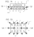
- FIGS. 1A and 1B display schematic views of two orthogonal cross sections along the axes 1 A- 1 A′ and 1 B- 1 B′ through an electronic system consisting of a semiconductor device 1 soldered to a printed circuit board 9 (PCB) via an array of solder bumps 12 .
- semiconductor device 1 is comprised of a semiconductor chip 2 that is packaged in a molded body 3 , and a two-dimensional array of solder bumps 12 that connect the semiconductor device 1 to the printed circuit board 9 .
- the molded body 3 is shaped to be of cubical shape having a flat first surface 11 facing the printed circuit board 9 , an opposing second surface 13 facing away from the printed circuit board 9 , and side faces connecting first and second surfaces 11 , 13 .
- the two-dimensional array of solder bumps 12 is attached to the flat first surface 11 of molded body 3 .
- the use of a two-dimensional array of solder bumps on the first surface 11 facilitates a high input/output channel density.
- the array of solder bumps 7 on the first surface 11 of the molded body 3 may serve two purposes: (a) if the solder bumps 12 are electronically connected to the integrated circuit in the semiconductor chip 2 , the solder bumps 12 may provide the electrical connection between the integrated circuit and the circuit on the PCB 9 , and (b) the array of solder bumps 12 provides a mechanical connection to rigidly hold the semiconductor device 1 to the printed circuit board 9 .
- FIGS. 1A and 1B also disclose mechanical forces, indicated by the arrows F, that act on the solder bumps 12 when printed circuit board 9 expands laterally at a higher rate than the semiconductor device 1 due to deviating coefficients of thermal expansion (CTE) of the materials involved.
- CTE coefficients of thermal expansion
- the CTE of silicon is only 3 ⁇ 10 ⁇ 6 1/K while the CTE of a PCB is in the range of 17 ⁇ 10 ⁇ 6 1/K.
- temperature cycles of the semiconductor device during device operation may generate shear forces on the solder bumps that may break the solder bumps away from the molded body 3 , which may cause the devices to fail.
- the lateral expansion of PCB 9 in FIG. 1A is indicated by a double-arrow labeled CTE.
- the shear forces F are directed in reverse directions.
- FIG. 1B by the lengths of the arrows assigned to the various solder bumps 12 , also indicates that the shear forces F are the larger the further away a solder bump is located away from the central solder bumps. This observation indicates that the risk of solder bumps breakage is the larger the larger the area of the solder bump array is. Further, the risk of solder bump breakage is highest for those solder bumps that are located at the outer edges of the solder bump array.
- FIGS. 2A and 2B disclose schematic views on two orthogonal cross sections along the axes 2 A- 2 A′ and 2 B- 2 B′ of an embodiment of a semiconductor device 10 comprising a semiconductor chip 2 , a molded body 3 that encapsulates the semiconductor chip 2 , an array of recesses 5 formed in a first surface 11 of the molded body 3 , first contact elements 7 , and elastic elements 14 in the recesses 5 that each connect one of the first contact elements 7 with the molded body 3 .
- Semiconductor chip 2 may contain an integrated circuit, a sensor, a micro-electromechanical system (MEMS), optical components or any other functional device that is integrated into the semiconductor chip.
- the semiconductor chip 2 has a thickness of a few hundred micrometers and a lateral extension of a few millimeters, or centimeters, in lateral directions (see FIG. 2B ).
- semiconductor chip 2 is fully encapsulated by molded body 3 .
- Encapsulating semiconductor chips in a molded body helps protecting the sensitive surfaces of the chip from harming environmental influences, like humidity, scratches and chemicals.
- molded body 3 has been formed from hot liquid molding material that has been introduced under pressure into a mold in which the chip 2 is inserted. During cooling, the molding material hardens to take on the shape of the mold.
- molded body 3 is a cubical with an array of ten column-like shaped recesses 5 on its first surface 11 .
- first surface 11 is a flat surface that provides sufficient space for placing a two-dimensional array of first contact elements 7 thereon.
- array of recesses may also refer to two-dimensional arrays that have missing elements therein.
- the mold material may be a polymer, e.g. an epoxy resin that, for CTE-adjustment, may contain a filling material, e.g. silicon oxide, and other components, like organic hardeners, release agents, adhesion promoters, flame retardants etc.
- the choice of the right molding material mixture, and the details of the molding process, depend on the application and are well known in the art.
- the elastic elements 14 each mechanically connect one first contact element 7 with molded body 5 .
- the elastic elements may be made of electrically insulating material
- the first contact elements 7 are made of conducting material to make electrical contact to the outside world, e.g., to a PCB board.
- the first contact elements 7 are made of a metal or alloy that can be soldered or welded to the conducting lines of, say, a printed circuit board.
- the first contact elements 7 may be layer elements made of copper or tin, solder bumps made of solder materials like Pb/Sn, and the like.
- First contact elements may be grown, deposited or placed on top of the elastic elements 14 .
- the shear forces between the semiconductor device 10 and the substrate to which the semiconductor device 10 is mounted can be absorbed to protect the first contact elements 7 from breaking away from molded body 3 .
- shear forces may arise on first contact elements 7 during device operation due to different CTEs of the semiconductor device and the substrate to which the substrate is mounted.
- the recesses 5 in the molded body 3 provide a large interface area for the elastic elements 14 to be bond to.
- a large interface area ensures good adhesion of the elastic element to the molded body 3 .
- the inner walls of the recesses 5 that enclose the respective elastic elements 14 make sure that the elastic elements 14 cannot break from the molded body 3 when shearing forces act on the first contact elements 7 . For this reason, it is useful if the elastic elements 14 are form-fit to the shape of the respective recesses.
- the term “recess” may stand for many different types of recesses. They may be holes, cavities, trenches, depressions, openings, or through-holes that reach from one face 11 of the molded body 3 to the opposite other face 3 of molded body 3 .
- the elastic elements 14 may be a body of any material that is sufficiently elastic to prevent breakage of the first contact element 7 from the molded body 3 under thermo-mechanical or mechanical strain. Generally, it is preferred that the elastic module of the material is less than 50 MPa. For high reliability or large package sizes (e.g. larger than 40 mm 2 ) the elastic module may be below 15 MPa. Further criteria for the selection of the material of the elastic elements 14 may be: (a) good adhesion of the elastic element material to the molded body; (b) good adhesion of the first contact element material to the elastic elements; and (c) overall process compatibility of the elastic element material during the manufacturing of the semiconductor device. In the embodiment of FIGS.
- the elastic elements 14 are made of silicone which can have an elastic module of typically 3 MPa to 15 MPa and up to approximately 50 MPa.
- the elastic modulus of the resilient material can be chosen depending on the needed flexibility, reliability or package size. Ways of implementing the silicone elastic elements 14 into the recesses will be explained later in more detail.
- the sizes of the elastic elements 14 generally depend on the contact element pitch requirements, and on the expected shear forces acting on the contact elements during manufacturing, mounting or device operation. The expected shear forces in turn depend on the size of the contact element array, on the diameters of the contact elements, on the CTE-values of the materials involved, etc. If the contact elements are solder bumps, the pitch between the solder bumps is typically in the range of 500-2000 micrometers, while the diameter of the solder bumps 12 is typically in the range of 300-1000 micrometers. Further, the elastic elements 14 that in FIGS. 2A and 2B have a column-like shape may have a column diameter that is larger than the diameter of the solder balls 12 .
- the columns are selected to be smaller than the pitch of the of the solder balls to avoid that neighboring elastic elements 14 touch each other.
- the height of the elastic element columns in FIGS. 2A and 2B is about as large as the diameter of elastic element columns. However, there is no limitation to the height of the elastic element columns as long as the shear forces can be absorbed sufficiently.
- each elastic element 14 protrudes from the first surface 11 of the molded body 3 .
- the distance between the molded body 3 and the substrate (not shown in FIGS. 2A and 2B ) to 5 which the semiconductor device is soldered is larger compared to systems where the elastic elements 14 do not protrude.
- a larger distance may help to absorb the shear forces better. This observation can be used to adjust the protrusion of the elastic elements 14 from the first surface 11 such that any given shear force requirement can be handled without that the solder bumps 12 break.
- the first contact elements in FIGS. 2A and 2B may be lead free solder bumps.
- the first contact elements 7 may also be conducting layer elements made of any conductive material, e.g. metals or compounds like e.g. copper, tin, tin-lead or palladium, that can be soldered to a printed circuit board, metal balls made of copper, tin, conductive polymer or metal coated polymer, studs made of copper, aluminum or gold or posts made of copper or any other material, etc.
- FIGS. 3 and 4 disclose cross sections of further embodiments of semiconductor devices 20 , 30 .
- the embodiment of FIG. 3 may be identical to the embodiment of FIGS. 2A and 2B with the difference that the elastic elements 14 are flush with first surface 11 of molded body 3 . Having the elastic elements 14 flush with the first surface 11 enables an efficient way of manufacturing, as will be described later in the description.
- the elastic elements 14 of semiconductor device 20 have a shape of a truncated cone with the base of the cone flush with first surface 11 .
- One of the advantages of this geometry is that it is easy to implement the elastic elements 14 into the recesses 5 .
- the large area of the cone base is capable of holding a large contact element 12 without having the contact element 12 touch molded body 3 .
- the first contact elements 7 are solder bumps 12 .
- the embodiment of FIG. 4 may be identical to the embodiment of FIG. 3 except that elastic elements 14 , instead of having the truncated cone pointing upwards, point in a downward direction.
- An advantage of this geometry is that the elastic elements 14 are mechanically interlocked with the molded body 3 . This way, the elastic elements 14 are securely tied to the molded body 3 to withstand strong shear forces.
- FIGS. 3 and 4 are to illustrate only some of the many shapes that can be chosen for the elastic elements 14 .
- FIGS. 2A-B , 3 and 4 disclose recesses 5 and elastic elements 14 that have a rotationally symmetric cross section
- recesses 5 and elastic elements 14 can also have cross sections that are squared, cubical or of any other shape appropriate for a given application or manufacturing process.
- the elastic elements 14 are form-fit to the shapes of the recesses, there may be circumstances where the elastic elements 14 fill the recess volumes only partially.
- FIGS. 5A and 5B disclose schematic views on two orthogonal cross sections along the axes 5 A- 5 A′ and 5 B- 5 B′ of a further embodiment of a semiconductor device 40 comprising a semiconductor chip 2 , a molded body 3 that encapsulates the semiconductor chip 2 , an array of recesses 5 in a flat first surface 11 of the of the molded body 3 .
- semiconductor device 40 comprises first contact elements 7 and elastic elements 14 in the recesses 5 that each mechanically connects one of the first contact elements 7 with molded body 3 .
- Shape and material of the molded body 3 , solder bumps 12 , semiconductor chip 2 , and elastic elements 14 may be the same as disclosed in FIGS. 2A , 2 B, 3 and 4 .
- FIGS. 5A and 5B differs over the previous embodiments in that first main face 104 of the semiconductor chip 2 is left free of molding material. Instead, molded body 3 covers the second main face 105 and the side faces of semiconductor chip 2 only. This way, connection elements 102 are left free of molding material.
- FIGS. 5A and 5B further differs over the previous embodiments in that first main face 104 of semiconductor chip 2 is flush with the elastic elements 14 and the planar first surface 11 of the molded body 3 .
- This package design has several advantages, one of them being that elastic elements 14 , first surface 11 of molded body 3 , and active surface 104 of semiconductor chip 2 form a coplanar plane 111 on which conducting lines 122 can be formed that connect the connection elements 102 of the semiconductor chip 2 with solder bumps 12 . Due to the planarity of coplanar plane 111 , the conducting lines 122 can be formed using highly efficient, and precise, planar technology processes, like metal layer deposition, lithography, and selective etching.
- conducting lines with a minimum structure size of less than twenty micrometer in lateral dimensions and thicknesses below 1 ⁇ m, typically 1-7 ⁇ m can be formed.
- Such small nominal structure size enables a production of thousands of connection lines 122 connecting the connection elements 102 of semiconductor chip 2 to possibly thousands of contact elements 7 within one layer.
- the cross section of FIG. 5B which is taken within coplanar plane 111 , illustrates schematically the way in which five of the ten solder bumps 12 are electrically connected to respective five of the ten connection elements 102 on semiconductor chip 2 .
- FIGS. 6A and 6B disclose schematic views on two orthogonal cross sections along the axes 6 A- 6 A′ and 6 B- 6 B′ of a further embodiment of a semiconductor device 50 that in many ways resembles that of FIGS. 5A and 5B .
- semiconductor device 50 in addition to the first contact elements 7 that are elastically connected to the molded body by means of elastic elements 14 , semiconductor device 50 also comprises second contact elements 17 that are rigidly connected to semiconductor chip 2 . This way, the active chip area 104 (first main face of the chip) can be used for additional input/output channels.
- semiconductor device 50 also comprises third contact elements 27 that in contrast to the other contact elements are rigidly connected to the molded body 3 .
- third contact elements 27 that in contrast to the other contact elements are rigidly connected to the molded body 3 .
- elastic elements 14 that is because the thermo-mechanically generated shear forces on the contact elements are largest at the outer contact elements of a contact element array. Therefore, it may be sufficient to have only the outer contact element line and row of the array elastically connected to molded body 3 while in the central region of the array of contact elements, a rigid connection of the molded body 3 to the substrate may be preferred to provide for better system robustness.
- FIGS. 7A to 7H disclose schematically an embodiment of a method of manufacturing semiconductor devices.
- FIG. 7A discloses a carrier 101 onto which semiconductor chips 2 and elastic elements 14 can be placed.
- carrier 101 may be any carrier that can be used as a basis for placing and molding semiconductor chips 2 .
- carrier 101 may be a bottom piece of a mold form, a foil on which the chips are positioned and molded, or a sticky tape with thermo-release properties.
- carrier 101 to be a double-sided sticky tape (not shown in FIG. 7A ) with thermo-release properties that is laminated onto a flat plate.
- the double-sided stickiness of the tape makes sure that the tape is securely held by the flat plate, and that the individual semiconductor chips 2 and elastic elements 14 can be securely placed onto predefined positions with high accuracy, e.g. with a spatial precision of about 10-15 micrometers (see FIG. 7B ).
- the individual chips 2 are placed onto the carrier 101 in an upside-down direction, i.e. the first main faces 104 of the chips 2 that comprise connection elements 102 (and the active region of the chip) are facing downwardly in a direction towards carrier 101 .
- the chips 2 are taken from a processed and singulated wafer, picked by a pick-and-place automate, and placed on carrier 101 .
- the elastic elements 14 in FIG. 7B are prefabricated elements made of silicone or any other elastomer.
- the prefabricated elements may be thermoplastic or thermosetting materials.
- the elastic elements may be flexibilized by addition of flexible materials of the same or a different material family.
- the material can be a foam as well.
- the elastic elements 14 have a truncated cone-like shape having a base diameter of, say, 500 micrometers and a height of, say, 200 micrometers.
- the base diameter of the elastic element is larger (typically 10-20% larger) than the pad diameter to which the contact element is applied.
- the reliability can be adapted by adapting the size of the elastic elements.
- the size of the elastic element is less than 10% larger than the pad (even smaller), for very large packages, the size of the elastic elements can be more than 20% larger than the pad.
- the thickness of the elastic element can range from 20 ⁇ m to chip thickness. With the cone-like shape, the elastic elements 14 have a sufficient base surface to securely adhere to the double-sided sticky tape of carrier 101 . It can have any other form as well.
- FIG. 7C schematically discloses the set-up of FIG. 7B after molding the semiconductor chips 2 in a compression molding process.
- a liquid molding compound e.g. a polymer or resin etc.
- a top cavity is moved downwardly towards the carrier to close the cavity, thereby spreading out the molding material until the cavity is filled completely.
- the molded material hardens to become molded body 3 .
- FIG. 7C discloses molded body 3 covering the second main face 105 and the sides of the semiconductor chips 2 and elastic elements 14 but, due to the first main faces 104 of the semiconductor chip 2 securely attached to carrier 101 , leaving the first main faces 104 and connection elements 102 free of molding material.
- molded body 3 may have any shape.
- the molded body 3 has been shaped by a mold form with a cavity having a height and lateral extension of a standard semiconductor wafer.
- the diameter may be 8 or 12 inches (200 mm or 300 mm), and the height may be typically 500 to 800 micrometers.
- molded body 3 , the elastic elements 14 and the semiconductor chips 2 covered by the molded body 3 form a “reconstituted wafer” 160 on which, with standard wafer processing equipment, can be conveniently deposited or structured additional layers.
- the molding can also be done by a more traditional method known as transfer molding, which is a widely used technique for the encapsulation of electronic devices.
- transfer molding is a widely used technique for the encapsulation of electronic devices.
- the principal of this technique is based on a thermally liquefied molding compound being transferred under pressure into a preformed cavity.
- FIG. 7D schematically discloses molded body 3 after having released carrier 101 from molded body 3 .
- the release may be conveniently carried out by heating the thermo-release tape.
- the first main surface 104 of the semiconductor chip 2 , the connection elements 102 , as well as the bases of the elastic elements 14 are exposed to the outside as no molded material is covering the three.
- the exposed first main surface 104 of the semiconductor chip 2 , the bases of the elastic elements 14 , and the molded body 3 form a flat coplanar plane 111 .
- the elastic elements 14 , and the semiconductor chips 2 embedded in the molded body 3 form a “reconstituted wafer” 160 .
- FIG. 7E schematically discloses reconstituted wafer 160 , after having been processed to obtain solder bumps 12 on top of the elastic elements 14 , and a redistribution layer that electrically connects the connection elements 102 of the semiconductor chips 2 to respective solder bumps 12 .
- the redistribution layer in FIG. 7E is comprised of conducting lines 122 that provide for the electrical connections between the connection elements 102 and the solder bumps 12 , elements of an insulation layer 124 that selectively insulate the surfaces of the semiconductor chips 2 from the conduction lines 122 , and solder stop layer 126 for shaping the solder bumps 12 at the right positions.
- FIG. 7F schematically discloses molded body of FIG. 7E after having been sawn to separate reconstituted wafer 160 into separated semiconductor devices 60 .
- the sawing process is a standard process well known in the art. Note that the sawing process is being performed after molding, and after application of the solder bumps 12 to the semiconductor devices 60 . This way, it is possible to carry out the molding process and the solder bump application on a wafer level, i.e. as a batch process where many semiconductor devices are manufactured in parallel.
- FIG. 7G discloses a section of the embodiment of FIG. 7F magnified to schematically illustrate the structure of the molded body 3 of FIG. 7F in the vicinity of the elastic elements 14 in more detail.
- elastic element 14 is form-fit to recess 5 of molded body 3 so that the boundary of recess 5 and elastic element 14 coincide. This is due to the fact that the elastic elements 14 have been placed onto carrier 101 before liquid molding material was applied over semiconductor chips 2 and elastic elements 14 . The liquid molding material was able to enclose the elastic elements 14 in a form-fit manner.
- FIG. 7G further discloses that the base of the cone-shaped elastic elements 14 and the lower face of the molded body 3 are flush with each other. This is due to the fact that elastic elements 14 (and the semiconductors chips 2 ) were placed on a flat carrier before molding material was applied over the elastic elements 14 and the semiconductor chips 2 .
- FIG. 7G further discloses that, after separating the carrier 101 from molded body 3 , an insulation layer 124 was applied over the surface of molded body 3 and the semiconductor chips 2 . Insulation layer 124 is to electrically insulate the conducting lines 122 from the semiconductor chip 2 wherever needed. In this embodiment, insulation layer 124 has been applied and structured on the wafer level, typically by using thin-film techniques, but printing or jetting technologies would be possible as well.
- the minimum structure size of insulation layer 124 may be as low as 10-20 micrometer (lateral size), while the thickness of the insulation layer 124 is in typically in the range of 5 to 15 micrometers.
- Materials that are used for the insulation materials are polymers, like polyimide, epoxies, BCB or PBOs or other known dielectric materials.
- the insulation layer 124 has been opened in the regions of the connection elements 102 of the semiconductor chips 2 , and in the regions of the elastic elements 14 .
- FIG. 7G further discloses conducting lines 122 applied on insulation layer 124 .
- the conducting lines 122 have been etched from a layer of conducting material, e.g. aluminum, copper, or stacks of metals, e.g. CuNiAu.
- the thickness of the conducting lines is typically 1 to 7 micrometers.
- the conducting lines 122 fully cover the openings in the insulation layer 12 . This way, a good electric connection is made between the connection elements 102 of the semiconductor chips 2 and the respective conducting line 122 .
- the conducting lines 122 form a base for the solder bumps 12 that are to be formed during the following processing steps.
- the conducting lines 122 can be used as “under bump metallization” (UBM).
- UBM under bump metallization
- additional UBM-layers may be applied over the base of the conducting lines 122 to prevent diffusion, oxidation and other chemical processes in the interface region of the solder bumps 12 and the conducting lines 122 .
- the UBM may consist of a conducting adhesion layer, a conducting wetting layer and/or a conducting oxidation barrier layer.
- FIG. 7G further discloses solder stop layer 126 , an insulating layer with openings in the solder bump base regions applied over the conducting layer 122 .
- Solder stop layer 126 may be of polymers, like polyimide, epoxies, BCB, PBOs or other known dielectric materials, having a thickness of typically a few micrometers. Solder stop layer 126 prevents solder material from expanding laterally over the surface of the redistribution layer when applying solder material, e.g. Pb/Sn, over the conducting lines. Solder stop layer 126 further helps to insulate the conducting lines against electrical contact with the outside of the semiconductor device.
- FIG. 7G further discloses solder bump 12 formed on top of conducting line 122 over elastic element 14 . It is preferred that solder bump 12 and elastic element 14 are centered around the same axis to provide the solder bumps 12 with the highest mechanical flexibility possible with respect to the molded body 3 .
- FIG. 7H schematically discloses the way in which elastic element 14 helps absorbing shear forces F acting on the solder bump. Due to the ability of the elastic elements 14 to deform under pressure, rigid solder bump 12 can intrude into the original volume of the elastic elements 14 to be bent into the direction of the shear force. This way, the force necessary to break a solder bump from the molded body cannot build up as easily as in the absence of the elastic elements 14 . Note that the conducting lines 122 , and the insulation layer 124 , due to their thin layer structures, are flexible enough to adjust to the deformation that the shear force F is causing to the elastic elements 14 .
- FIGS. 8A to 8H schematically disclose a further embodiment of a method of manufacturing a semiconductor device.
- the method is the same as explained in the embodiment of FIGS. 7A to 7F . Therefore, for the same features in the drawings, the same labeling is used.
- recesses 5 and elastic elements 14 are formed in molded body 3 after the semiconductor chips 2 have been molded.
- FIG. 8A corresponds to FIG. 7B with the exception that no elastic elements 14 are placed on carrier 101 .
- FIG. 8B corresponds to FIG. 7C .
- molding material is applied over the semiconductor chips 2 to form molded body 3 .
- FIG. 8C discloses molded body 3 after the carrier has been removed from molded body 3 , as described for FIG. 7D . After removal, semiconductor chips 2 and molded body 3 form a reconstituted wafer 160 with the first main faces 104 of semiconductor chips 2 exposed to the outside. The exposed first main faces 104 form a coplanar plane 111 with molded body 3 .
- FIG. 8D schematically discloses molded body 3 after recesses 5 , or holes, have been etched selectively to a photo-lithographically structured mask 112 into molded body 3 , on coplanar plane 111 .
- the diameters and depths of the recesses 5 are comparable to the geometry of the elastic elements 14 that are to be formed in the recesses 5 .
- FIG. 8E schematically discloses molded body 3 of FIG. 8D after removal of mask 112 .
- Remaining molded body 3 represent a reconstituted wafer 160 with recesses 5 ready to be filled with elastic material 14 a.
- FIG. 8F discloses one embodiment wherein elastic material 14 a (e.g. silicone or any other elastomer, thermoplastic or thermosetting material) is selectively dispensed into the recesses 5 by a dispensing tool 131 in a standard ink jet process.
- elastic material 14 a e.g. silicone or any other elastomer, thermoplastic or thermosetting material
- the elastic material is usually heated, e.g. at 180° C., or radiated to solidify and to adhere to the recess walls.
- a silicone material known in the art is, e.g., ElastosilTM by Wacker Company.
- elastic material 14 a may be filled into the recesses 5 by applying the elastic material selectively to the photo-lithographically structured mask 112 (see FIG. 8D ), or selectively to a template (screen printing) that has its openings aligned to the recesses 5 . After application of the selective material 14 a , the mask or template are removed to leave only the recesses 5 covered with elastic material 14 a (see FIG. 8F ). After solidification, the elastic material 14 a turns into elastic elements 14 . Note that in FIG. 8F , the shape of the elastic elements 14 is that of a column, conforming to the shape of the recesses 5 etched in molded body 3 .
- FIG. 8G schematically discloses reconstituted wafer 160 of FIG. 8F after a redistribution layer (comprised of insulation layer 124 , conducting layer 122 , and solder stop layer 126 ) has been applied over the coplanar plane 111 , after solder bumps 12 have been applied over the elastic elements 14 , and after the reconstituted wafer has been sawn into separated semiconductor devices 70 .
- a redistribution layer (comprised of insulation layer 124 , conducting layer 122 , and solder stop layer 126 ) has been applied over the coplanar plane 111 , after solder bumps 12 have been applied over the elastic elements 14 , and after the reconstituted wafer has been sawn into separated semiconductor devices 70 .
- FIGS. 9A to 9F schematically disclose a further embodiment of a method of manufacturing semiconductor devices.
- the method is the same as explained in the embodiment of FIGS. 7A to 7F .
- recesses 5 are formed in molded body 3 by means of a carrier 101 that comprises protrusions 144 that protrude from the surface on which the molding material is to be applied.
- the protrusions 144 are conically shaped in order to form cone-shaped recesses in the molded body 3 when applying molding material over carrier (see FIG. 9B ).
- the shape of the protrusions 144 can be of other geometries as well, e.g. column-like shaped, truncated cone-shaped, cubical, etc.
- the protrusions 144 may be part of the double-sided sticky tape that was used in the description of FIGS. 7A-7F . In this case, it is easy to remove the molded body 3 from the tape despite the protrusions 144 , due to the thermo-releasable properties of the tape. Alternatively, the protrusions 144 may be part of a mold form in which the semiconductor chips 2 are molded.
- FIG. 9B discloses the semiconductor chips 2 after having been molded in molded body 3 .
- the mold form that has formed the molded body 3 has a cavity of a semiconductor wafer shape, i.e. a height of typically a few hundred micrometers, and a diameter of, say, 200 mm or 300 mm. This way, a reconstituted wafer consisting of semiconductor chips 2 embedded in a molding material matrix can be formed.
- FIG. 9C discloses molded body 3 after having been removed from carrier 101 to become a reconstituted wafer 160 .
- the carrier 101 being a thermo-releasable tape
- molded body 3 has been removed from the carrier 101 by a heating procedure.
- reconstituted wafer 160 consists of the molded body 3 and semiconductor chips 2 whose first main faces 104 and connection elements 102 are exposed to the outside. Further, first main faces 104 and molded body 3 form a coplanar plane 111 , interrupted solely by the cone-shaped recesses 5 .
- FIG. 9D discloses reconstituted wafer 160 after having filled the recesses 5 with elastic material to obtain elastic elements 14 in the recesses 5 .
- the filling of the recesses 5 with elastic material can be done in the same way as described in the embodiment of FIGS. 8A to 8G .
- the elastic material may be silicone or any other elastomer, thermoplastic or thermosetting materials.
- FIG. 9E schematically discloses molded body 3 of FIG. 9D after a redistribution layer (comprised of insulation layer 124 , conducting layer 122 , and solder stop layer 126 ) has been applied over coplanar plane 111 , after solder bumps 12 have been applied over the elastic elements 14 , and after reconstituted wafer 160 has been sawn to become multiple separated semiconductor devices 80 .
- a redistribution layer (comprised of insulation layer 124 , conducting layer 122 , and solder stop layer 126 ) has been applied over coplanar plane 111
- solder bumps 12 have been applied over the elastic elements 14
- reconstituted wafer 160 has been sawn to become multiple separated semiconductor devices 80 .
Abstract
Description
Claims (20)
Priority Applications (3)
| Application Number | Priority Date | Filing Date | Title |
|---|---|---|---|
| US11/850,750 US7868446B2 (en) | 2007-09-06 | 2007-09-06 | Semiconductor device and methods of manufacturing semiconductor devices |
| DE102008038175A DE102008038175B4 (en) | 2007-09-06 | 2008-08-18 | Semiconductor arrangement and method for the production of semiconductor devices |
| KR1020080083814A KR101015726B1 (en) | 2007-09-06 | 2008-08-27 | Semiconductor device and method of manufacturing semiconductor devices |
Applications Claiming Priority (1)
| Application Number | Priority Date | Filing Date | Title |
|---|---|---|---|
| US11/850,750 US7868446B2 (en) | 2007-09-06 | 2007-09-06 | Semiconductor device and methods of manufacturing semiconductor devices |
Publications (2)
| Publication Number | Publication Date |
|---|---|
| US20090065927A1 US20090065927A1 (en) | 2009-03-12 |
| US7868446B2 true US7868446B2 (en) | 2011-01-11 |
Family
ID=40430961
Family Applications (1)
| Application Number | Title | Priority Date | Filing Date |
|---|---|---|---|
| US11/850,750 Expired - Fee Related US7868446B2 (en) | 2007-09-06 | 2007-09-06 | Semiconductor device and methods of manufacturing semiconductor devices |
Country Status (3)
| Country | Link |
|---|---|
| US (1) | US7868446B2 (en) |
| KR (1) | KR101015726B1 (en) |
| DE (1) | DE102008038175B4 (en) |
Cited By (3)
| Publication number | Priority date | Publication date | Assignee | Title |
|---|---|---|---|---|
| US20150145126A1 (en) * | 2009-11-25 | 2015-05-28 | Stats Chippac, Ltd. | Semiconductor Device and Method of Forming Compliant Stress Relief Buffer Around Large Array WLCSP |
| US9064787B2 (en) | 2010-10-28 | 2015-06-23 | Infineon Technologies Ag | Integrated antennas in wafer level package |
| US11094649B2 (en) | 2020-01-21 | 2021-08-17 | Advanced Semiconductor Engineering, Inc. | Semiconductor package structure and method for manufacturing the same |
Families Citing this family (13)
| Publication number | Priority date | Publication date | Assignee | Title |
|---|---|---|---|---|
| TWI339865B (en) * | 2007-08-17 | 2011-04-01 | Chipmos Technologies Inc | A dice rearrangement package method |
| KR20100058345A (en) * | 2008-11-24 | 2010-06-03 | 삼성전자주식회사 | Methods of forming camera modules |
| US8278749B2 (en) | 2009-01-30 | 2012-10-02 | Infineon Technologies Ag | Integrated antennas in wafer level package |
| US9202769B2 (en) | 2009-11-25 | 2015-12-01 | Stats Chippac, Ltd. | Semiconductor device and method of forming thermal lid for balancing warpage and thermal management |
| US9385095B2 (en) | 2010-02-26 | 2016-07-05 | Taiwan Semiconductor Manufacturing Company, Ltd. | 3D semiconductor package interposer with die cavity |
| US10056267B2 (en) * | 2014-02-14 | 2018-08-21 | Taiwan Semiconductor Manufacturing Company, Ltd. | Substrate design for semiconductor packages and method of forming same |
| US10026671B2 (en) | 2014-02-14 | 2018-07-17 | Taiwan Semiconductor Manufacturing Company, Ltd. | Substrate design for semiconductor packages and method of forming same |
| US9653443B2 (en) | 2014-02-14 | 2017-05-16 | Taiwan Semiconductor Manufacturing Company, Ltd. | Thermal performance structure for semiconductor packages and method of forming same |
| US9768090B2 (en) | 2014-02-14 | 2017-09-19 | Taiwan Semiconductor Manufacturing Company, Ltd. | Substrate design for semiconductor packages and method of forming same |
| US9935090B2 (en) | 2014-02-14 | 2018-04-03 | Taiwan Semiconductor Manufacturing Company, Ltd. | Substrate design for semiconductor packages and method of forming same |
| KR102081684B1 (en) * | 2014-08-26 | 2020-04-28 | 데카 테크놀로지 잉크 | Front side package-level serialization for packages comprising unique identifiers |
| US9564416B2 (en) | 2015-02-13 | 2017-02-07 | Taiwan Semiconductor Manufacturing Company, Ltd. | Package structures and methods of forming the same |
| US9985010B2 (en) | 2015-05-22 | 2018-05-29 | Qualcomm Incorporated | System, apparatus, and method for embedding a device in a faceup workpiece |
Citations (21)
| Publication number | Priority date | Publication date | Assignee | Title |
|---|---|---|---|---|
| JP2000031191A (en) | 1998-07-15 | 2000-01-28 | Mitsui High Tec Inc | Semiconductor device |
| US6118179A (en) * | 1999-08-27 | 2000-09-12 | Micron Technology, Inc. | Semiconductor component with external contact polymer support member and method of fabrication |
| DE10105351A1 (en) | 2001-02-05 | 2002-08-22 | Infineon Technologies Ag | Electronic component used as a storage component comprises a semiconductor chip having an intermediate connecting structure on its active surface |
| US6441500B1 (en) | 1999-09-13 | 2002-08-27 | Sharp Kabushiki Kaisha | Semiconductor device having resin members provided separately corresponding to externally connecting electrodes |
| US6515356B1 (en) * | 1999-05-07 | 2003-02-04 | Amkor Technology, Inc. | Semiconductor package and method for fabricating the same |
| US6518675B2 (en) | 2000-12-29 | 2003-02-11 | Samsung Electronics Co., Ltd. | Wafer level package and method for manufacturing the same |
| US6587353B2 (en) | 2000-05-25 | 2003-07-01 | Sharp Kabushiki Kaisha | Semiconductor device |
| US6713880B2 (en) * | 2001-02-07 | 2004-03-30 | Matsushita Electric Industrial Co., Ltd. | Semiconductor device and method for producing the same, and method for mounting semiconductor device |
| US20040142505A1 (en) | 2003-01-21 | 2004-07-22 | Siliconware Precision Industries Co., Ltd. | Semiconductor package free of substrate and fabrication method thereof |
| US20060012024A1 (en) * | 2000-10-13 | 2006-01-19 | Bridge Semiconductor Corporation | Semiconductor chip assembly with metal containment wall and solder terminal |
| US7022549B2 (en) | 2002-12-30 | 2006-04-04 | Infineon Technologies, Ag | Method for connecting an integrated circuit to a substrate and corresponding arrangement |
| US7071027B2 (en) | 2003-01-29 | 2006-07-04 | Samsung Electronics Co., Ltd. | Ball grid array package having improved reliability and method of manufacturing the same |
| US20060145344A1 (en) * | 2005-01-05 | 2006-07-06 | Yoshihiko Shimanuki | Semiconductor device |
| US20070069389A1 (en) | 2005-09-15 | 2007-03-29 | Alexander Wollanke | Stackable device, device stack and method for fabricating the same |
| US20070090528A1 (en) * | 2005-05-12 | 2007-04-26 | Nec Corporation | Device, and manufacturing method for the device |
| US7211472B2 (en) | 2003-09-30 | 2007-05-01 | Infineon Technologies Ag | Method for producing a multichip module and multichip module |
| US20070114642A1 (en) * | 2002-05-30 | 2007-05-24 | Fujitsu Limited | Semiconductor device having a heat spreader exposed from a seal resin |
| US20070164433A1 (en) * | 2003-07-31 | 2007-07-19 | Bloom Terry R | Ball grid array package |
| US7265449B2 (en) * | 2004-08-23 | 2007-09-04 | Samsung Electronics Co., Ltd. | Tape circuit substrate, semiconductor chip package including the same, and liquid crystal display device including the semiconductor chip package |
| US20090032964A1 (en) * | 2007-07-31 | 2009-02-05 | Micron Technology, Inc. | System and method for providing semiconductor device features using a protective layer |
| US7498670B2 (en) * | 2002-08-29 | 2009-03-03 | Micron Technology, Inc. | Semiconductor structures having electrophoretically insulated vias |
-
2007
- 2007-09-06 US US11/850,750 patent/US7868446B2/en not_active Expired - Fee Related
-
2008
- 2008-08-18 DE DE102008038175A patent/DE102008038175B4/en not_active Expired - Fee Related
- 2008-08-27 KR KR1020080083814A patent/KR101015726B1/en not_active IP Right Cessation
Patent Citations (21)
| Publication number | Priority date | Publication date | Assignee | Title |
|---|---|---|---|---|
| JP2000031191A (en) | 1998-07-15 | 2000-01-28 | Mitsui High Tec Inc | Semiconductor device |
| US6515356B1 (en) * | 1999-05-07 | 2003-02-04 | Amkor Technology, Inc. | Semiconductor package and method for fabricating the same |
| US6118179A (en) * | 1999-08-27 | 2000-09-12 | Micron Technology, Inc. | Semiconductor component with external contact polymer support member and method of fabrication |
| US6441500B1 (en) | 1999-09-13 | 2002-08-27 | Sharp Kabushiki Kaisha | Semiconductor device having resin members provided separately corresponding to externally connecting electrodes |
| US6587353B2 (en) | 2000-05-25 | 2003-07-01 | Sharp Kabushiki Kaisha | Semiconductor device |
| US20060012024A1 (en) * | 2000-10-13 | 2006-01-19 | Bridge Semiconductor Corporation | Semiconductor chip assembly with metal containment wall and solder terminal |
| US6518675B2 (en) | 2000-12-29 | 2003-02-11 | Samsung Electronics Co., Ltd. | Wafer level package and method for manufacturing the same |
| DE10105351A1 (en) | 2001-02-05 | 2002-08-22 | Infineon Technologies Ag | Electronic component used as a storage component comprises a semiconductor chip having an intermediate connecting structure on its active surface |
| US6713880B2 (en) * | 2001-02-07 | 2004-03-30 | Matsushita Electric Industrial Co., Ltd. | Semiconductor device and method for producing the same, and method for mounting semiconductor device |
| US20070114642A1 (en) * | 2002-05-30 | 2007-05-24 | Fujitsu Limited | Semiconductor device having a heat spreader exposed from a seal resin |
| US7498670B2 (en) * | 2002-08-29 | 2009-03-03 | Micron Technology, Inc. | Semiconductor structures having electrophoretically insulated vias |
| US7022549B2 (en) | 2002-12-30 | 2006-04-04 | Infineon Technologies, Ag | Method for connecting an integrated circuit to a substrate and corresponding arrangement |
| US20040142505A1 (en) | 2003-01-21 | 2004-07-22 | Siliconware Precision Industries Co., Ltd. | Semiconductor package free of substrate and fabrication method thereof |
| US7071027B2 (en) | 2003-01-29 | 2006-07-04 | Samsung Electronics Co., Ltd. | Ball grid array package having improved reliability and method of manufacturing the same |
| US20070164433A1 (en) * | 2003-07-31 | 2007-07-19 | Bloom Terry R | Ball grid array package |
| US7211472B2 (en) | 2003-09-30 | 2007-05-01 | Infineon Technologies Ag | Method for producing a multichip module and multichip module |
| US7265449B2 (en) * | 2004-08-23 | 2007-09-04 | Samsung Electronics Co., Ltd. | Tape circuit substrate, semiconductor chip package including the same, and liquid crystal display device including the semiconductor chip package |
| US20060145344A1 (en) * | 2005-01-05 | 2006-07-06 | Yoshihiko Shimanuki | Semiconductor device |
| US20070090528A1 (en) * | 2005-05-12 | 2007-04-26 | Nec Corporation | Device, and manufacturing method for the device |
| US20070069389A1 (en) | 2005-09-15 | 2007-03-29 | Alexander Wollanke | Stackable device, device stack and method for fabricating the same |
| US20090032964A1 (en) * | 2007-07-31 | 2009-02-05 | Micron Technology, Inc. | System and method for providing semiconductor device features using a protective layer |
Non-Patent Citations (1)
| Title |
|---|
| Brunnbauer et al., Embedded Wafer Level Ball Grid Array (eWLB); 2006 Electronics Packaging Technology Conference, 1-4244-0665-X/06, IEEE, 2006 (pp. 1-5). |
Cited By (4)
| Publication number | Priority date | Publication date | Assignee | Title |
|---|---|---|---|---|
| US20150145126A1 (en) * | 2009-11-25 | 2015-05-28 | Stats Chippac, Ltd. | Semiconductor Device and Method of Forming Compliant Stress Relief Buffer Around Large Array WLCSP |
| US9508621B2 (en) * | 2009-11-25 | 2016-11-29 | STATS ChipPAC Pte. Ltd. | Semiconductor device and method of forming compliant stress relief buffer around large array WLCSP |
| US9064787B2 (en) | 2010-10-28 | 2015-06-23 | Infineon Technologies Ag | Integrated antennas in wafer level package |
| US11094649B2 (en) | 2020-01-21 | 2021-08-17 | Advanced Semiconductor Engineering, Inc. | Semiconductor package structure and method for manufacturing the same |
Also Published As
| Publication number | Publication date |
|---|---|
| DE102008038175A1 (en) | 2010-02-25 |
| DE102008038175B4 (en) | 2011-07-07 |
| KR20090026050A (en) | 2009-03-11 |
| US20090065927A1 (en) | 2009-03-12 |
| KR101015726B1 (en) | 2011-02-22 |
Similar Documents
| Publication | Publication Date | Title |
|---|---|---|
| US7868446B2 (en) | Semiconductor device and methods of manufacturing semiconductor devices | |
| US9455161B2 (en) | Semiconductor device and methods of manufacturing semiconductor devices | |
| CN107887343B (en) | Semiconductor package structure and manufacturing method thereof | |
| CN109786340B (en) | Integrated fan-out package and method of forming the same | |
| JP5579402B2 (en) | Semiconductor device, method for manufacturing the same, and electronic device | |
| TWI426542B (en) | Semiconductor device with three-dimensional stacked structure and method of fabricating same | |
| US8183677B2 (en) | Device including a semiconductor chip | |
| US9984900B2 (en) | Semiconductor device including at least one element | |
| EP3288077B1 (en) | Microelectronic package having a bumpless laminated interconnection layer | |
| US8138020B2 (en) | Wafer level integrated interconnect decal and manufacturing method thereof | |
| US20130069218A1 (en) | High density package interconnect with copper heat spreader and method of making the same | |
| EP1662566A2 (en) | Semiconductor device and method of fabricating the same | |
| KR101067060B1 (en) | Die package having encapsulated die and method of manufacturing the same | |
| KR101837511B1 (en) | Semiconductor package and method of manufacturing the same | |
| JP2011061004A (en) | Semiconductor device, and method of manufacturing the same | |
| US20120077312A1 (en) | Flip-chip bonding method to reduce voids in underfill material | |
| CN112310063A (en) | Semiconductor device package and method of manufacturing the same | |
| US9334156B2 (en) | Chip package and method thereof | |
| JP2011243724A (en) | Semiconductor device and method for manufacturing the same | |
| US20070196952A1 (en) | Manufacturing method of semiconductor device | |
| JP2002313993A (en) | Semiconductor device, its mounting method, and its junction structure | |
| US20170178993A1 (en) | Electronic component and methods of manufacturing the same | |
| CN111883505A (en) | Electronic package, bearing substrate thereof and manufacturing method |
Legal Events
| Date | Code | Title | Description |
|---|---|---|---|
| AS | Assignment |
Owner name: INFINEON TECHNOLOGIES AG, GERMANY Free format text: ASSIGNMENT OF ASSIGNORS INTEREST;ASSIGNOR:MEYER, THORSTEN;REEL/FRAME:021093/0416 Effective date: 20070905 |
|
| FEPP | Fee payment procedure |
Free format text: PAYOR NUMBER ASSIGNED (ORIGINAL EVENT CODE: ASPN); ENTITY STATUS OF PATENT OWNER: LARGE ENTITY |
|
| AS | Assignment |
Owner name: INTEL MOBILE COMMUNICATIONS TECHNOLOGY GMBH, GERMA Free format text: ASSIGNMENT OF ASSIGNORS INTEREST;ASSIGNOR:INFINEON TECHNOLOGIES AG;REEL/FRAME:027548/0623 Effective date: 20110131 |
|
| AS | Assignment |
Owner name: INTEL MOBILE COMMUNICATIONS GMBH, GERMANY Free format text: ASSIGNMENT OF ASSIGNORS INTEREST;ASSIGNOR:INTEL MOBILE COMMUNICATIONS TECHNOLOGY GMBH;REEL/FRAME:027556/0709 Effective date: 20111031 |
|
| FPAY | Fee payment |
Year of fee payment: 4 |
|
| AS | Assignment |
Owner name: INTEL DEUTSCHLAND GMBH, GERMANY Free format text: CHANGE OF NAME;ASSIGNOR:INTEL MOBILE COMMUNICATIONS GMBH;REEL/FRAME:037057/0061 Effective date: 20150507 |
|
| FEPP | Fee payment procedure |
Free format text: MAINTENANCE FEE REMINDER MAILED (ORIGINAL EVENT CODE: REM.); ENTITY STATUS OF PATENT OWNER: LARGE ENTITY |
|
| LAPS | Lapse for failure to pay maintenance fees |
Free format text: PATENT EXPIRED FOR FAILURE TO PAY MAINTENANCE FEES (ORIGINAL EVENT CODE: EXP.); ENTITY STATUS OF PATENT OWNER: LARGE ENTITY |
|
| STCH | Information on status: patent discontinuation |
Free format text: PATENT EXPIRED DUE TO NONPAYMENT OF MAINTENANCE FEES UNDER 37 CFR 1.362 |
|
| FP | Lapsed due to failure to pay maintenance fee |
Effective date: 20190111 |
|
| AS | Assignment |
Owner name: INTEL CORPORATION, CALIFORNIA Free format text: ASSIGNMENT OF ASSIGNORS INTEREST;ASSIGNOR:INTEL DEUTSCHLAND GMBH;REEL/FRAME:061356/0001 Effective date: 20220708 |