US7878860B1 - Modular connector system - Google Patents
Modular connector system Download PDFInfo
- Publication number
- US7878860B1 US7878860B1 US12/770,348 US77034810A US7878860B1 US 7878860 B1 US7878860 B1 US 7878860B1 US 77034810 A US77034810 A US 77034810A US 7878860 B1 US7878860 B1 US 7878860B1
- Authority
- US
- United States
- Prior art keywords
- assembly
- contact
- insulator
- end portion
- adapter
- Prior art date
- Legal status (The legal status is an assumption and is not a legal conclusion. Google has not performed a legal analysis and makes no representation as to the accuracy of the status listed.)
- Active
Links
Images


Classifications
-
- H—ELECTRICITY
- H01—ELECTRIC ELEMENTS
- H01R—ELECTRICALLY-CONDUCTIVE CONNECTIONS; STRUCTURAL ASSOCIATIONS OF A PLURALITY OF MUTUALLY-INSULATED ELECTRICAL CONNECTING ELEMENTS; COUPLING DEVICES; CURRENT COLLECTORS
- H01R13/00—Details of coupling devices of the kinds covered by groups H01R12/70 or H01R24/00 - H01R33/00
- H01R13/46—Bases; Cases
- H01R13/502—Bases; Cases composed of different pieces
-
- H—ELECTRICITY
- H01—ELECTRIC ELEMENTS
- H01R—ELECTRICALLY-CONDUCTIVE CONNECTIONS; STRUCTURAL ASSOCIATIONS OF A PLURALITY OF MUTUALLY-INSULATED ELECTRICAL CONNECTING ELEMENTS; COUPLING DEVICES; CURRENT COLLECTORS
- H01R12/00—Structural associations of a plurality of mutually-insulated electrical connecting elements, specially adapted for printed circuits, e.g. printed circuit boards [PCB], flat or ribbon cables, or like generally planar structures, e.g. terminal strips, terminal blocks; Coupling devices specially adapted for printed circuits, flat or ribbon cables, or like generally planar structures; Terminals specially adapted for contact with, or insertion into, printed circuits, flat or ribbon cables, or like generally planar structures
- H01R12/70—Coupling devices
- H01R12/71—Coupling devices for rigid printing circuits or like structures
- H01R12/712—Coupling devices for rigid printing circuits or like structures co-operating with the surface of the printed circuit or with a coupling device exclusively provided on the surface of the printed circuit
- H01R12/716—Coupling device provided on the PCB
-
- H—ELECTRICITY
- H01—ELECTRIC ELEMENTS
- H01R—ELECTRICALLY-CONDUCTIVE CONNECTIONS; STRUCTURAL ASSOCIATIONS OF A PLURALITY OF MUTUALLY-INSULATED ELECTRICAL CONNECTING ELEMENTS; COUPLING DEVICES; CURRENT COLLECTORS
- H01R31/00—Coupling parts supported only by co-operation with counterpart
- H01R31/06—Intermediate parts for linking two coupling parts, e.g. adapter
-
- H—ELECTRICITY
- H01—ELECTRIC ELEMENTS
- H01R—ELECTRICALLY-CONDUCTIVE CONNECTIONS; STRUCTURAL ASSOCIATIONS OF A PLURALITY OF MUTUALLY-INSULATED ELECTRICAL CONNECTING ELEMENTS; COUPLING DEVICES; CURRENT COLLECTORS
- H01R13/00—Details of coupling devices of the kinds covered by groups H01R12/70 or H01R24/00 - H01R33/00
- H01R13/62—Means for facilitating engagement or disengagement of coupling parts or for holding them in engagement
- H01R13/629—Additional means for facilitating engagement or disengagement of coupling parts, e.g. aligning or guiding means, levers, gas pressure electrical locking indicators, manufacturing tolerances
- H01R13/631—Additional means for facilitating engagement or disengagement of coupling parts, e.g. aligning or guiding means, levers, gas pressure electrical locking indicators, manufacturing tolerances for engagement only
- H01R13/6315—Additional means for facilitating engagement or disengagement of coupling parts, e.g. aligning or guiding means, levers, gas pressure electrical locking indicators, manufacturing tolerances for engagement only allowing relative movement between coupling parts, e.g. floating connection
Definitions
- the present invention generally relates to apparatuses for interconnecting circuit boards or other electrical components.
- the adapter assembly comprises: an adapter housing; a first insulator in the form of a generally rectangular solid block having a plurality of through holes; a first set of contacts, each contact in said first set being disposed in one of said though holes such that and an end portion of the contact extends beyond a surface of the first insulator, which end portion is configured to mate with a corresponding contact of the header assembly; a second insulator in the form of a generally rectangular solid block having a plurality of through holes; and a second set of contacts, each contact in said second set being disposed in one of said though holes of said second insulator such that and an end portion of the contact extends beyond a surface of the second insulator, which end portion is configured to mate with a corresponding contact of the header assembly.
- the header assembly comprises: a header housing; a third insulator in the form of a generally rectangular solid block having a plurality of through holes; a third set of contacts, each contact in said third set (a) having a first end portion and a second end portion, said first end portion being configured to mate with a corresponding element of the circuit board and the second end portion being directly connected to a contact from the first set of contacts and (b) being disposed in one of said though holes such that the first end portion of the contact extends beyond a surface of the third insulator; a fourth insulator in the form of a generally rectangular solid block having a plurality of through holes; and a fourth set of contacts, each contact in said fourth set (a) having a first end portion and a second end portion, said first end portion being configured to mate with a corresponding element of the circuit board and the second end portion being directly connected to a contact from the second set of contacts and (b) being disposed in one of said though holes such that the first end portion of the contact
- a float plate is attached to the adapter assembly.
- the float plate may be configured to floatably connect the adapter assembly to a frame.
- the adapter housing comprises means for facilitating alignment of the header assembly with the adapter assembly
- the header housing comprises means for facilitating alignment of the header assembly with the adapter assembly
- the third and fourth insulator each comprises means for facilitating alignment of the header assembly with the adapter assembly.
- FIGS. 1-26 illustrate a connector system according to embodiments of the invention.
- FIGS. 27-39 illustrate a connector system according to another embodiment of the invention.
- FIGS. 40-42 illustrate a connector system according to yet another embodiment of the invention.
- FIGS. 43-45 illustrate a connector system according to yet another embodiment of the invention.
- FIG. 1 illustrates a connector system 100 according to an embodiment of the invention.
- connector system 100 may include a first connector assembly 101 a electrically connected to a second connector assembly 101 b .
- Connector assembly 101 a may be substantially identical to connector assembly 101 b .
- system 100 may include a plug 108 electrically connected to connector assembly 101 b .
- Each connector assembly 101 i.e., connector assemblies 101 a,b
- Each assembly 101 may also include a float plate 106 for connecting the adapter assembly 104 to a frame (e.g., a chassis) or other device. Float plate 106 may be configured to snap onto adapter assembly 104 .
- FIG. 2 is a top view of an exemplary connector assembly 101 .
- header assembly 102 of the connector assembly 101 may include a header housing 202
- adapter assembly 104 may also include an adapter housing 204 for housing various insulators (i.e., housings that house contacts and electrically insulate the contacts from one another).
- adapter housing 204 is housing two power/RF insulators 211 and a signal insulator 212
- the power/RF insulators 211 are housing two power contacts 220 and two signal contacts 222
- the signal insulator 212 is housing a number of signal contacts 222 .
- FIG. 3 is a bottom view of the exemplary connector assembly 101 .
- housing 202 is housing two power/RF insulators 311 and a signal insulator 312
- the power/RF insulators 311 are housing two power contacts 320 and two signal contacts 322
- the signal insulator 312 is housing a number of signal contacts 322 .
- FIG. 4 is a side view of connector assembly 101 .
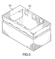
- FIG. 5 is a view of an exemplary adapter housing 204 .
- housing 204 is a generally rectangular housing open at opposite side thereof having two end walls and two side walls, and the side walls include grooves 502 for receiving a locking tab 602 (see FIG. 6 ) formed on a side wall of an insulator.
- the depth of the groove 502 decreases as the groove 502 proceeds inwardly, thereby forming a ramp structure. This facilitates the locking of an insulator in the adapter housing.
- FIG. 6 illustrates three insulators and the locking tab 602 .
- the locking tab 602 is configured to engage groove 502 , as illustrated in FIGS. 7 and 8 .
- insulators 211 and 212 are generally in the form of rectangular, solid blocks that include through holes for receiving a contact.
- power/RF insulator 211 includes, in the embodiment shown, two through holes 611 each for receiving a power contact or RF contact and two through holes 612 each for receiving a signal contact.
- signal insulator 212 includes, in the embodiment shown, eighteen through holes 614 for receiving eighteen signal contacts.
- FIG. 9 is a top view of adapter assembly 104 and shows an exemplary signal contact 222 inserted into a through hole 614 of signal insulator 212 .
- FIG. 9 also shows an exemplary power contact 220 inserted into a through hole 611 of power insulator 212 .
- FIG. 10 is a bottom view of adapter assembly 104 and shows that an end portion of power contact 220 and an end portion of signal contact 222 passes entirely through the through holes 611 and 614 , respectively. That is the end portions of contacts 220 and 222 extend beyond the bottom face of insulators 211 and 212 , respectively. Insulators 211 and 212 and contacts 220 and 222 configured like this so that the end portions of the contacts can mate with corresponding contacts of the header assembly 102 .
- adapter assembly 104 has having two power insulators 211 and a single signal insulator 212 arranged between the power insulators, the invention is not so limited.
- an advantage of adapter assembly 104 is that it is extremely adaptable. That is, the type of insulators that may be housed in adapter housing 204 and the arrangement of said insulators in the housing is entirely up to the end user. Some users may desire three power insulators and no signal insulators, while others may prefer the opposite or some other combination and arrangements of insulators.
- FIG. 11 illustrates an exemplary signal contact 222 .
- the exemplary signal contact 222 is elongate, has a conical tip 1102 (a.k.a., lead in 1102 ), and a open, crimpable end portion 1104 for receiving a corresponding electrical element (e.g., the end of a wire).
- end portion 1104 is in a crimped state and, therefore, has a generally C shaped cross section. In an uncrimped state, end portion 1104 would have a more U shaped cross section.
- FIG. 12 illustrates an exemplary power contact 220 , which, in the embodiment shown, includes a conical shaped lead-in 1202 , which functions to facilitate alignment between assemblies 102 and 104 .
- FIG. 13 illustrates an exemplary header assembly 102 .
- header assembly includes a header housing 202 for housing power/RF insulators 311 and/or signal insulators 312 .
- header assembly 102 also includes a signal insulator 312 sandwiched between two power insulators 311 .
- FIG. 14 further illustrates header housing 202 .
- header housing 202 includes a generally rectangular frame 1402 having two parallel end walls and two parallel side walls, and the side walls include grooves 1404 for receiving a locking tab (see e.g., element 602 in FIG. 6 ) formed on a side wall of an insulator.
- the depth of the groove 1404 decreases as the groove 502 proceeds inwardly, thereby forming a ramp structure. This facilitates the locking of an insulator in the header housing 202 .
- housing 202 includes two parallel side walls 1306 , 1308 that face each other and extend outwardly from the end walls of housing 1402 .
- FIG. 15 shows a signal insulator 312 that has been inserted into housing 202 . Groove 1404 and lock tab 602 engage to releasably retain insulator 312 in housing 202 .
- FIG. 16 shows an exemplary signal contact 322 inserted into a through hole of signal insulator 312 .
- FIG. 16 also shows an exemplary power contact 320 inserted into a through hole of power insulator 312 .
- FIG. 17 is a cross-sectional view of assembly 102 according to some embodiments. In the embodiment shown, the end portion 1702 of contact is disposed within the though hole. That is, in the embodiment shown, end portion 1702 does not extend beyond the upper face 1704 of signal insulator 312 .
- FIG. 18 further illustrates contact 312 according to some embodiments.
- contact 322 is elongate, has a male compliant end 1802 for solderless mating with a corresponding through hole in a circuit board, and has a female end 1702 for receiving conical tip of signal contact 222 .
- FIG. 20 shows compliant (solderless) power contact 320 according to some embodiments.
- FIG. 20 is a cross-sectional view of connector assembly 101 showing adapter assembly 104 mated with header assembly 102 .
- the adapters of header assembly 102 are positioned within the cavity formed by housing 204 and the bottom faces of insulators 211 / 212 , which cavity is best seen in FIG. 10 , the signal contacts 222 engage with the signal contacts 322 , thereby electrically coupling the signal contacts, and the contacts 220 engage with contacts 320 .
- header assembly 102 and adapter assembly 104 include means for facilitating alignment of the header assembly 102 with the adapter assembly when the two are blind mated.
- one such means is the float plate 106 attached to adapter assembly 104 .
- Float plate 106 has a through hole 107 for receiving a screw or pin (e.g., shoulder screw) (not shown) that is used to floatably connect adapter assembly to a chassis or other component.
- adapter assembly 104 is preferably not rigidly connected to the chassis, but rather connected so that it has some radial and/or axial float relative to the chassis.
- adapter assembly can move position relative to the chassis and relative to the header assembly 102 to thereby achieve alignment.
- FIG. 21 shows housings 202 and 204 just prior to engagement and serves to illustrate how the beveled edge 1002 and beveled edges 1302 , 1304 facilitate alignment.
- Still further means include the conical shaping of lead-in 1102 and the conical shaping of lead-in 1202 .
- through holes 614 are sized to allow contacts 222 to float slightly.
- the signal contact through holes 2204 of signal insulator 312 have beveled edges 2206 , as shown in FIG. 22 .
- other means for facilitating the correct alignment include beveled edges 2201 and 2202 of insulators 311 and 312 , respectively.
- FIGS. 23-26 these figures illustrate a process for making connector system 100 .
- the process begins by connecting an end of a wire (e.g., insulated wire) to a contact 222 a and connecting the other end of the wire to signal contact 222 b . This step is repeated as many times as necessary. After this step, contact 222 b is inserted into signal insulator 212 b and contact 222 a is inserted into a signal insulator 212 a as shown in FIG. 21 . Again, this step may be repeated until there are no more empty though holes in the insulators. Next, insulators 212 a,b are inserted into adapter housings 204 a,b respectively, as shown in FIG. 23 .
- a wire e.g., insulated wire
- insulators as needed may also be inserted into housings 204 a,b .
- housings 204 a,b respectively, a first power insulator 211 a and a second power insulator 211 b , wherein, prior to insertion, insulator 211 a houses a power contact 220 a that is electrically connected via a wire (or other means) to a power contact 220 b housed in insulator 211 b .
- adapter assemblies 104 a,b are mated with corresponding header assemblies 102 a,b , respectively, such that the contacts of adapter assemblies 104 a,b engage with corresponding contacts of header assemblies 102 a,b , respectively (see FIG. 24 ).
- the process of connecting plug 108 (see FIG. 1 ) to connector assembly 102 b is similar. That is, for example, one end of a wire (e.g., wire 109 ) is attached to an end of a signal contact 222 b and then the signal contact is inserted into an insulator through hole (e.g., hole 612 or 614 ). Preferably the step of inserting the contact in the through hole occurs prior to inserting in the adapter housing 204 b the particular insulator in which the through hole is formed. The other end of the wire 109 may be connected to plug 108 or any other component.
- a wire e.g., wire 109
- an insulator through hole e.g., hole 612 or 614
- the step of inserting the contact in the through hole occurs prior to inserting in the adapter housing 204 b the particular insulator in which the through hole is formed.
- the other end of the wire 109 may be connected to plug 108 or any other component.
- FIG. 27 illustrates a connector system 2500 according to another embodiment.
- connector system 2700 may include a first connector assembly 2701 a electrically connected to a second connector assembly 2701 b .
- Connector assembly 2701 a may be substantially identical to connector assembly 2701 b .
- Each connector assembly 2701 i.e., connector assemblies 2701 a,b
- Each assembly 2701 may also include a float plate 2706 for connecting the adapter assembly 2704 to a chassis or other device.
- FIG. 28 is a top view of an exemplary connector assembly 2701 .
- header assembly 2702 of the connector assembly 2701 may include a header housing 202 and adapter assembly 2704 may also include an adapter housing 2804 for housing various insulators (i.e., housings that house contacts and electrically insulate the contacts from one another).
- adapter housing 2804 is housing two power/RF insulators 211 and three signal insulators 212 , the power/RF insulators 211 may house an RF contact 2820 and two signal contacts 222 , and the signal insulator 212 may house a number of signal contacts 222 (e.g., eighteen signal contacts).
- FIG. 29 is a bottom view of the exemplary connector assembly 2701 .
- housing 2802 is housing two power/RF insulators 311 and three signal insulators 312
- the power/RF insulators 311 are housing two power contacts 320 and two signal contacts 322
- the signal insulators 312 are housing a number of signal contacts 322 .
- FIG. 30 is a side view of connector assembly 2701 .
- FIG. 31 is a view of an exemplary adapter housing 2804 .
- housing 2804 is a generally rectangular housing open at opposite side thereof having two end walls and two side walls, and the side walls include grooves 502 for receiving a locking tab 602 (see FIG. 6 ) formed on a side wall of an insulator.
- the depth of the groove 502 decreases as the groove 502 proceeds inwardly, thereby forming a ramp structure. This facilitates the locking of an insulator in the adapter housing.
- FIG. 32 is a top view of adapter assembly 2704 and shows an exemplary signal contact 222 inserted into a through hole 614 of signal insulator 212 .
- FIG. 9 also shows an exemplary RF contact 2820 inserted into a through hole 611 of power/RF insulator 212 .
- FIG. 33 is a bottom view of adapter assembly 2704 and shows that an end portion of RF contact 2820 and an end portion of signal contact 222 passes entirely through the through holes 611 and 614 , respectively. That is the end portions of contacts 2820 and 222 extend beyond the bottom face of insulators 211 and 212 , respectively. Insulators 211 and 212 and contacts 2820 and 222 configured like this so that the end portions of the contacts can mate with corresponding contacts of the header assembly 2702 .
- adapter assembly 2704 has having two power insulators 211 and three single signal insulators 212 arranged between the power insulators, the invention is not so limited. In fact, an advantage of adapter assembly 2704 is that it is extremely adaptable. That is, the type of insulators that may be housed in adapter housing 204 and the arrangement of said insulators in the housing is entirely up to the end user.
- FIG. 34 illustrates an exemplary RF contact 2820 , which, in the embodiment shown, includes a conical shaped lead-in 3402 , which functions to facilitate alignment between assemblies 2702 and 2704 .
- FIG. 35 is an exploded view of RF contact 2820 according to some embodiments.
- RF contact 2820 includes: a clamp nut 3501 ; a crimp sleeve 3502 ; a dielectric (e.g., a Teflon dielectric) 3503 ; a signal contact 3504 and an outer body 3505 .
- FIG. 36 is a cross-sectional view of the RF connector shown in FIGS. 34 and 35 .
- FIG. 37 illustrates an exemplary header assembly 2702 .
- header assembly includes a header housing 2802 for housing power/RF insulators 311 and/or signal insulators 312 .
- header assembly 2702 also includes three signal insulators 312 sandwiched between two power insulators 311 .
- FIG. 38 further illustrates header housing 2802 .
- Header housing 2802 includes a generally rectangular frame 3802 having two parallel end walls and two parallel side walls, and the side walls include grooves 1404 for receiving a locking tab (see e.g., element 602 in FIG. 6 ) formed on a side wall of an insulator.
- housing 2802 includes two parallel side walls 3706 , 3708 that face each other and extend outwardly from the end walls of frame 3802 .
- FIG. 39 illustrates RF contact 2920 according to some embodiments.
- RF contact includes: a compliant member 3901 ; a dielectric 3902 ; a signal contact 3903 ; a outer contact 3904 and a n outer body 3905 .
- header assembly 2702 and adapter assembly 2704 include features that facilitate alignment of the header assembly with the adapter assembly when the two are blind mated.
- float plate 2706 is attached to adapter assembly 2704 and is used to floatably connect adapter assembly to a chassis or other component.
- Other features that facilitate correct alignment include an internal beveled edge 3302 (see FIG. 33 ) of adapter housing 2804 and beveled forward edges 3702 , 3704 formed on walls 3706 and 3708 , respectively.
- Still further features include the conical shaping of lead-in 3402 .
- FIG. 40 illustrates a connector assembly 4001 according to another embodiment.
- connector assembly 4001 may include a header assembly 4002 and an adapter assembly 4004 .
- adapter assembly 4004 is also a header assembly because it is designed to connect directly to a printed circuit board, but to avoid confusion we shall refer to assembly 4004 as the adapter assembly 4004 .
- Connector assembly 4001 is almost identical to connector assembly 2701 .
- connector assembly 4001 includes: (a) an adapter housing 4094 for housing insulators 211 and 212 in the same manner that housing 2804 houses the insulators and (b) header housing 2802 for housing insulators 311 and 312 .
- a difference between connector assembly 4001 and connector assembly 2701 is that different contacts are housed in the insulators. For example, as shown in FIG. 40 , insulator 211 holds power contacts 4020 , insulator 212 holds signal contacts 4022 , insulator 311 holds power contacts 4021 , and insulator 312 holds signal contacts 4023 .
- FIG. 41 further illustrates signal contacts 4022 and 4023 .
- contact 4022 is elongate and its tips 4103 , 4104 are conical.
- contact 4023 is elongate and has a conical tip 4101 .
- the other end of contact 4023 defines an opening for receiving end 4103 of contact 4022 .
- FIG. 42 further illustrates power contacts 4020 and 4021 .
- FIG. 43 illustrates a connector assembly 4301 according to another embodiment.
- connector assembly 4301 may include header assembly 4002 and an adapter assembly 4304 .
- Adapter assembly 4304 is nearly identical to header assembly 2704 .
- adapter assembly 4304 includes adapter housing 4304 for housing insulators 211 , 212 .
- a difference between adapter assembly 4304 and adapter assembly 2704 is that adapter assembly includes different contacts than adapter assembly 2704 .
- insulator 211 holds power contacts 4320
- insulator 212 holds signal contacts 4322 .
- FIG. 44 further illustrates signal contact 4322 .
- contact 4322 is elongate and has a conical tip 4401 .
- the other end of contact 4322 defines an opening for receiving another contact (e.g., the end of a wire)
- FIG. 45 shows exploded views of power contacts 4021 and 4320 .
- contact 4021 includes an dielectric 4502 for housing a contact 4501 .
- Power contact 4320 includes: a contact element 4503 ; a rear body 4504 ; a front contact 4505 ; and a dielectric 4506 .
Abstract
Description
Claims (5)
Priority Applications (2)
| Application Number | Priority Date | Filing Date | Title |
|---|---|---|---|
| US12/770,348 US7878860B1 (en) | 2010-04-29 | 2010-04-29 | Modular connector system |
| US13/017,607 US8206179B2 (en) | 2010-04-29 | 2011-01-31 | Modular connector system |
Applications Claiming Priority (1)
| Application Number | Priority Date | Filing Date | Title |
|---|---|---|---|
| US12/770,348 US7878860B1 (en) | 2010-04-29 | 2010-04-29 | Modular connector system |
Related Child Applications (1)
| Application Number | Title | Priority Date | Filing Date |
|---|---|---|---|
| US13/017,607 Continuation US8206179B2 (en) | 2010-04-29 | 2011-01-31 | Modular connector system |
Publications (1)
| Publication Number | Publication Date |
|---|---|
| US7878860B1 true US7878860B1 (en) | 2011-02-01 |
Family
ID=43501887
Family Applications (2)
| Application Number | Title | Priority Date | Filing Date |
|---|---|---|---|
| US12/770,348 Active US7878860B1 (en) | 2010-04-29 | 2010-04-29 | Modular connector system |
| US13/017,607 Active US8206179B2 (en) | 2010-04-29 | 2011-01-31 | Modular connector system |
Family Applications After (1)
| Application Number | Title | Priority Date | Filing Date |
|---|---|---|---|
| US13/017,607 Active US8206179B2 (en) | 2010-04-29 | 2011-01-31 | Modular connector system |
Country Status (1)
| Country | Link |
|---|---|
| US (2) | US7878860B1 (en) |
Cited By (5)
| Publication number | Priority date | Publication date | Assignee | Title |
|---|---|---|---|---|
| US20130252458A1 (en) * | 2010-08-30 | 2013-09-26 | Phoenix Contact Gmbh & Co. Kg | Electrical component |
| US20160149362A1 (en) * | 2014-11-21 | 2016-05-26 | Tyco Electronics Corporation | Connector brick for cable communication system |
| US20160359259A1 (en) * | 2014-02-20 | 2016-12-08 | Harting Electric Gmbh & Co. Kg | Contact carrier |
| US20200021070A1 (en) * | 2018-07-12 | 2020-01-16 | Illinois Tool Works Inc. | Reconfigurable welding-type power sockets and power plugs |
| US10700450B2 (en) | 2018-09-21 | 2020-06-30 | Winchester Interconnect Corporation | RF connector |
Families Citing this family (1)
| Publication number | Priority date | Publication date | Assignee | Title |
|---|---|---|---|---|
| US9305837B2 (en) * | 2014-04-10 | 2016-04-05 | Taiwan Semiconductor Manufacturing Company Limited | Semiconductor arrangement and formation thereof |
Citations (9)
| Publication number | Priority date | Publication date | Assignee | Title |
|---|---|---|---|---|
| US5772450A (en) | 1996-07-23 | 1998-06-30 | Litton Systems, Inc. | Electrical connectors having external circuit connections |
| US20050161254A1 (en) | 2004-01-26 | 2005-07-28 | Litton Systems, Inc. | Multilayered circuit board for high-speed, differential signals |
| US20080014801A1 (en) * | 2003-11-14 | 2008-01-17 | Luc Milette | Wire guide and connector assembly using same |
| US20080242154A1 (en) * | 2007-03-28 | 2008-10-02 | Dixon Steven C | Powered, Mobile Electronics Mount |
| US20090093138A1 (en) | 2007-10-08 | 2009-04-09 | Winchester Electronics Corporation | Modular interconnect apparatus |
| US7572148B1 (en) * | 2008-02-07 | 2009-08-11 | Tyco Electronics Corporation | Coupler for interconnecting electrical connectors |
| US7625243B2 (en) * | 2007-06-13 | 2009-12-01 | Hon Hai Precision Ind. Co., Ltd. | Extension to version 2.0 universal serial bus connector with improved contact arrangement |
| US7731519B1 (en) * | 2004-02-17 | 2010-06-08 | Trans-A-Matic, Inc. | Adaptable universal electrical connector system particularly adapted for use in repair or replacement of electrical components such as relays, solenoids and the like |
| US7798726B2 (en) * | 2008-08-22 | 2010-09-21 | Hon Hai Precision Ind. Co., Ltd. | Electrical connector with improved signal transmission means |
Family Cites Families (9)
| Publication number | Priority date | Publication date | Assignee | Title |
|---|---|---|---|---|
| US5498175A (en) * | 1994-01-06 | 1996-03-12 | Yeh; Ming-Hwa | Coaxial cable connector |
| US7270578B2 (en) * | 2005-12-02 | 2007-09-18 | Zippy Technology Corp. | Power supply power compensation structure |
| US7393249B2 (en) * | 2006-04-21 | 2008-07-01 | Trompeter Electronics, Inc. | Interconnection and monitoring module |
| US7782632B2 (en) * | 2006-05-30 | 2010-08-24 | Hewlett-Packard Development Company, L.P. | Electrical power connection with two power connectors on a module in an electronic system |
| DE102006033323A1 (en) * | 2006-07-17 | 2008-01-24 | Kostal Kontakt Systeme Gmbh | Electrical connector |
| US7455548B2 (en) * | 2006-10-19 | 2008-11-25 | Adc Telecommunication, Inc. | Rotatable connector modules with inverted jacks |
| TW200910701A (en) * | 2007-08-22 | 2009-03-01 | Delta Electronics Inc | Stacked combination connector and connector assembly |
| JP5060385B2 (en) * | 2008-05-09 | 2012-10-31 | 富士通コンポーネント株式会社 | Balanced transmission connector and balanced transmission cable connector |
| FR2931306B1 (en) * | 2008-05-15 | 2012-04-27 | Radiall Sa | MULTICONTACT CONNECTOR WITH INTEGRATED ROTATING LOCKING PART |
-
2010
- 2010-04-29 US US12/770,348 patent/US7878860B1/en active Active
-
2011
- 2011-01-31 US US13/017,607 patent/US8206179B2/en active Active
Patent Citations (10)
| Publication number | Priority date | Publication date | Assignee | Title |
|---|---|---|---|---|
| US5772450A (en) | 1996-07-23 | 1998-06-30 | Litton Systems, Inc. | Electrical connectors having external circuit connections |
| US20080014801A1 (en) * | 2003-11-14 | 2008-01-17 | Luc Milette | Wire guide and connector assembly using same |
| US20050161254A1 (en) | 2004-01-26 | 2005-07-28 | Litton Systems, Inc. | Multilayered circuit board for high-speed, differential signals |
| US7731519B1 (en) * | 2004-02-17 | 2010-06-08 | Trans-A-Matic, Inc. | Adaptable universal electrical connector system particularly adapted for use in repair or replacement of electrical components such as relays, solenoids and the like |
| US20080242154A1 (en) * | 2007-03-28 | 2008-10-02 | Dixon Steven C | Powered, Mobile Electronics Mount |
| US7625243B2 (en) * | 2007-06-13 | 2009-12-01 | Hon Hai Precision Ind. Co., Ltd. | Extension to version 2.0 universal serial bus connector with improved contact arrangement |
| US20090093138A1 (en) | 2007-10-08 | 2009-04-09 | Winchester Electronics Corporation | Modular interconnect apparatus |
| US7699617B2 (en) | 2007-10-08 | 2010-04-20 | Winchester Electronics Corporation | Modular interconnect apparatus |
| US7572148B1 (en) * | 2008-02-07 | 2009-08-11 | Tyco Electronics Corporation | Coupler for interconnecting electrical connectors |
| US7798726B2 (en) * | 2008-08-22 | 2010-09-21 | Hon Hai Precision Ind. Co., Ltd. | Electrical connector with improved signal transmission means |
Non-Patent Citations (1)
| Title |
|---|
| International Search Report and Written Opinion issued on Jun. 22, 2010 in International application No. PCT/US2010/033008, 6 pages. |
Cited By (9)
| Publication number | Priority date | Publication date | Assignee | Title |
|---|---|---|---|---|
| US20130252458A1 (en) * | 2010-08-30 | 2013-09-26 | Phoenix Contact Gmbh & Co. Kg | Electrical component |
| US9583879B2 (en) * | 2010-08-30 | 2017-02-28 | Phoenix Contact Gmbh & Co. Kg | Electrical component |
| US20160359259A1 (en) * | 2014-02-20 | 2016-12-08 | Harting Electric Gmbh & Co. Kg | Contact carrier |
| US9966689B2 (en) * | 2014-02-20 | 2018-05-08 | Harting Electric Gmbh & Co. Kg | Contact carrier |
| US20160149362A1 (en) * | 2014-11-21 | 2016-05-26 | Tyco Electronics Corporation | Connector brick for cable communication system |
| US10136196B2 (en) | 2014-11-21 | 2018-11-20 | Te Connectivity Corporation | Connector brick for cable communication system |
| US20200021070A1 (en) * | 2018-07-12 | 2020-01-16 | Illinois Tool Works Inc. | Reconfigurable welding-type power sockets and power plugs |
| US11894642B2 (en) * | 2018-07-12 | 2024-02-06 | Illinois Tool Works Inc. | Reconfigurable welding-type power sockets and power plugs |
| US10700450B2 (en) | 2018-09-21 | 2020-06-30 | Winchester Interconnect Corporation | RF connector |
Also Published As
| Publication number | Publication date |
|---|---|
| US20110269327A1 (en) | 2011-11-03 |
| US8206179B2 (en) | 2012-06-26 |
Similar Documents
| Publication | Publication Date | Title |
|---|---|---|
| US5466171A (en) | Polarizing system for a blind mating electrical connector assembly | |
| US9379472B2 (en) | Electric connector with accommodating shorting terminal | |
| US8206179B2 (en) | Modular connector system | |
| US9356374B2 (en) | Float adapter for electrical connector | |
| US9318838B2 (en) | Terminal and electrical connector with same | |
| US20100041266A1 (en) | Power connector with integrated signal connector | |
| US7354282B2 (en) | Electrical connector having blade terminals | |
| US9806443B1 (en) | Press-fit circuit board connector | |
| JP6259517B2 (en) | System with multiple plug-in connectors and multiple plug-in connectors | |
| US9293877B2 (en) | Interface adapter | |
| CN110326169B (en) | Male and female integrated pin and socket connector | |
| US7604518B2 (en) | Electrical contact with retention latch | |
| US4725240A (en) | Electrical socket | |
| US20080200073A1 (en) | Encoding device for connectors | |
| EP1571733B1 (en) | Electrical connector | |
| US7794289B1 (en) | Circuit board connector assembly | |
| US11843192B2 (en) | High voltage contact system | |
| US20160240948A1 (en) | Power Connector | |
| US11843200B2 (en) | Connector with a position assurance element having a contact receptacle | |
| US20130090018A1 (en) | Cable connector | |
| WO2011136779A1 (en) | Modular connector system | |
| CN105789945B (en) | Floating adapter for electrical connector | |
| EP1063732A1 (en) | Press pin ground | |
| EP3542420B1 (en) | Press-fit circuit board connector | |
| US6517388B1 (en) | Line connecter with permanent or temporary screw clamp |
Legal Events
| Date | Code | Title | Description |
|---|---|---|---|
| AS | Assignment |
Owner name: WINCHESTER ELECTRONICS CORPORATION, CONNECTICUT Free format text: ASSIGNMENT OF ASSIGNORS INTEREST;ASSIGNORS:OUELLETTE, DAVID A.;BENHAM, JOHN E.;REEL/FRAME:024598/0611 Effective date: 20100517 |
|
| STCF | Information on status: patent grant |
Free format text: PATENTED CASE |
|
| AS | Assignment |
Owner name: MADISON CAPITAL FUNDING LLC, AS AGENT, ILLINOIS Free format text: SECURITY AGREEMENT;ASSIGNOR:WINCHESTER ELECTRONICS CORPORATION;REEL/FRAME:028634/0754 Effective date: 20120725 |
|
| FPAY | Fee payment |
Year of fee payment: 4 |
|
| AS | Assignment |
Owner name: CIT FINANCE LLC, NEW YORK Free format text: SECURITY INTEREST;ASSIGNORS:WINCHESTER ELECTRONICS CORPORATION;CLEMENTS NATIONAL COMPANY;TRU CORPORATION;AND OTHERS;REEL/FRAME:034280/0547 Effective date: 20141117 |
|
| AS | Assignment |
Owner name: WINCHESTER ELECTRONICS CORPORATION, CONNECTICUT Free format text: RELEASE BY SECURED PARTY;ASSIGNOR:MADISON CAPITAL FUNDING LLC;REEL/FRAME:034201/0812 Effective date: 20141117 |
|
| AS | Assignment |
Owner name: WINCHESTER ELECTRONICS CORPORATION, CONNECTICUT Free format text: RELEASE BY SECURED PARTY;ASSIGNOR:MADISON CAPITAL FUNDING LLC;REEL/FRAME:034210/0469 Effective date: 20141117 |
|
| AS | Assignment |
Owner name: WILMINGTON TRUST, NATIONAL ASSOCIATION, AS COLLATE Free format text: SECOND LIEN SECURITY AGREEMENT;ASSIGNORS:WINCHESTER ELECTRONICS CORPORATION;TRU CORPORATION;SRI HERMETICS LLC;AND OTHERS;REEL/FRAME:034306/0792 Effective date: 20141117 |
|
| AS | Assignment |
Owner name: ANTARES CAPITAL LP, AS ADMINISTRATIVE AGENT, ILLIN Free format text: SECURITY INTEREST;ASSIGNORS:CLEMENTS NATIONAL COMPANY;SRI HERMETICS, LLC;TRU CORPORATION;AND OTHERS;REEL/FRAME:039218/0344 Effective date: 20160630 |
|
| AS | Assignment |
Owner name: WINCHESTER ELECTRONICS CORPORATION, CONNECTICUT Free format text: RELEASE BY SECURED PARTY;ASSIGNOR:WILMINGTON TRUST, NATIONAL ASSOCIATION;REEL/FRAME:039234/0013 Effective date: 20160630 Owner name: CLEMENTS NATIONAL COMPANY, CONNECTICUT Free format text: RELEASE BY SECURED PARTY;ASSIGNOR:WILMINGTON TRUST, NATIONAL ASSOCIATION;REEL/FRAME:039234/0013 Effective date: 20160630 Owner name: TRU CORPORATION, CONNECTICUT Free format text: RELEASE BY SECURED PARTY;ASSIGNOR:WILMINGTON TRUST, NATIONAL ASSOCIATION;REEL/FRAME:039234/0013 Effective date: 20160630 Owner name: SRI HERMETICS, LLC, CONNECTICUT Free format text: RELEASE BY SECURED PARTY;ASSIGNOR:WILMINGTON TRUST, NATIONAL ASSOCIATION;REEL/FRAME:039234/0013 Effective date: 20160630 |
|
| AS | Assignment |
Owner name: CLEMENTS NATIONAL COMPANY, CONNECTICUT Free format text: RELEASE BY SECURED PARTY;ASSIGNOR:CIT FINANCE LLC;REEL/FRAME:039379/0882 Effective date: 20160630 Owner name: SRI HERMETICS, LLC, CONNECTICUT Free format text: RELEASE BY SECURED PARTY;ASSIGNOR:CIT FINANCE LLC;REEL/FRAME:039379/0882 Effective date: 20160630 Owner name: TRU CORPORATION, CONNECTICUT Free format text: RELEASE BY SECURED PARTY;ASSIGNOR:CIT FINANCE LLC;REEL/FRAME:039379/0882 Effective date: 20160630 Owner name: WINCHESTER ELECTRONICS CORPORATION, CONNECTICUT Free format text: RELEASE BY SECURED PARTY;ASSIGNOR:CIT FINANCE LLC;REEL/FRAME:039379/0882 Effective date: 20160630 |
|
| AS | Assignment |
Owner name: WINCHESTER INTERCONNECT CORPORATION, DELAWARE Free format text: CHANGE OF NAME;ASSIGNOR:WINCHESTER ELECTRONICS CORPORATION;REEL/FRAME:046214/0895 Effective date: 20171130 |
|
| MAFP | Maintenance fee payment |
Free format text: PAYMENT OF MAINTENANCE FEE, 8TH YEAR, LARGE ENTITY (ORIGINAL EVENT CODE: M1552) Year of fee payment: 8 |
|
| AS | Assignment |
Owner name: TRU CORPORATION, CONNECTICUT Free format text: RELEASE BY SECURED PARTY;ASSIGNOR:ANTARES CAPITAL LP, AS COLLATERAL AGENT;REEL/FRAME:047878/0322 Effective date: 20181024 Owner name: WINCHESTER ELECTRONICS CORPORATION, CONNECTICUT Free format text: RELEASE BY SECURED PARTY;ASSIGNOR:ANTARES CAPITAL LP, AS COLLATERAL AGENT;REEL/FRAME:047878/0322 Effective date: 20181024 Owner name: CLEMENTS NATIONAL COMPANY, CONNECTICUT Free format text: RELEASE BY SECURED PARTY;ASSIGNOR:ANTARES CAPITAL LP, AS COLLATERAL AGENT;REEL/FRAME:047878/0322 Effective date: 20181024 Owner name: SRI HERMETICS, LLC, CONNECTICUT Free format text: RELEASE BY SECURED PARTY;ASSIGNOR:ANTARES CAPITAL LP, AS COLLATERAL AGENT;REEL/FRAME:047878/0322 Effective date: 20181024 |
|
| MAFP | Maintenance fee payment |
Free format text: PAYMENT OF MAINTENANCE FEE, 12TH YEAR, LARGE ENTITY (ORIGINAL EVENT CODE: M1553); ENTITY STATUS OF PATENT OWNER: LARGE ENTITY Year of fee payment: 12 |