US7890694B2 - Latched address multi-chunk write to EEPROM - Google Patents
Latched address multi-chunk write to EEPROM Download PDFInfo
- Publication number
- US7890694B2 US7890694B2 US12/469,531 US46953109A US7890694B2 US 7890694 B2 US7890694 B2 US 7890694B2 US 46953109 A US46953109 A US 46953109A US 7890694 B2 US7890694 B2 US 7890694B2
- Authority
- US
- United States
- Prior art keywords
- data
- sub
- address
- arrays
- chunk
- Prior art date
- Legal status (The legal status is an assumption and is not a legal conclusion. Google has not performed a legal analysis and makes no representation as to the accuracy of the status listed.)
- Expired - Fee Related
Links
Images


Classifications
-
- G—PHYSICS
- G11—INFORMATION STORAGE
- G11C—STATIC STORES
- G11C16/00—Erasable programmable read-only memories
- G11C16/02—Erasable programmable read-only memories electrically programmable
- G11C16/06—Auxiliary circuits, e.g. for writing into memory
- G11C16/08—Address circuits; Decoders; Word-line control circuits
-
- G—PHYSICS
- G11—INFORMATION STORAGE
- G11C—STATIC STORES
- G11C16/00—Erasable programmable read-only memories
- G11C16/02—Erasable programmable read-only memories electrically programmable
- G11C16/06—Auxiliary circuits, e.g. for writing into memory
- G11C16/10—Programming or data input circuits
-
- G—PHYSICS
- G11—INFORMATION STORAGE
- G11C—STATIC STORES
- G11C8/00—Arrangements for selecting an address in a digital store
- G11C8/12—Group selection circuits, e.g. for memory block selection, chip selection, array selection
Definitions
- This invention relates in general to data write circuits for memory devices and in particular, to a multi-chunk data write circuit and method for concurrently writing more than one addressable chunk of data at a time to an electrically-erasable and programmable read-only memory (EEPROM).
- EEPROM electrically-erasable and programmable read-only memory
- a multi-chunk write operation includes several repetitions of providing an address and a data chunk to be written at that address, then programming and verifying the programming of the data chunk into that address. Since the time for programming and verifying the programming of each chunk of data generally far exceeds the time required for providing the address and the data for each chunk of data, such multi-chunk write operations in a conventional EEPROM tend to be very slow.
- one aspect is a multi-chunk write circuit which concurrently writes and verifies the writing of multiple chunks of data at a time into an EEPROM, thereby performing multi-chunk write operations significantly faster than conventional EEPROM write circuits which sequentially write a chunk of data at a time into an EEPROM.
- Another aspect is a circuit for concurrently writing data into selected ones of a plurality of subarrays of EEPROM cells. Included in the circuit are means for storing a plurality of addresses indicative of locations in the plurality of subarrays of EEPROM cells; a plurality of data registers coupled to the plurality of subarrays of EEPROM cells; and means for sequentially storing addresses into the storing means and corresponding data into the plurality of data registers, and concurrently writing the data stored in the plurality of data registers into the locations in the plurality of subarrays corresponding to the stored addresses.
- a method of concurrently writing a plurality of data chunks into an EEPROM comprises the steps of: sequentially storing the plurality of data chunks into a plurality of data storage means respectively coupled to corresponding subarrays of the EEPROM; providing row and column select signals to row and column decoder means coupled to the corresponding subarrays of the EEPROM; and concurrently writing the plurality of data chunks stored in the plurality of data storage means into the corresponding subarrays of the EEPROM as indicated by the row and column select signals.
- FIGS. 1 and 2 illustrate, as comparative examples, timing diagrams for a prior art multiple chunk write operation, and a multi-chunk write operation utilizing aspects of the present invention
- FIG. 3 illustrates, as an example, a block diagram of an EEPROM system utilizing aspects of the present invention
- FIG. 4 illustrates, as an example, a block diagram of the write control logic of FIG. 3 , utilizing aspects of the present invention
- FIG. 5 illustrates, as an example, timing diagrams for a serial input (SI) signal and associated control signals (PD and MS) provided to the write control logic of FIG. 4 , utilizing aspects of the present invention
- FIG. 6 illustrates, as an example, a block diagram of the address latches, latch enable, and multiplexer of the write control logic circuit of FIG. 5 , utilizing aspects of the present invention
- FIG. 7 illustrates, as an example, a logic diagram of a quadrant decoder of the latch enable circuit of FIG. 5 , utilizing aspects of the present invention
- FIG. 8 illustrates, as an example, a logic diagram of an address latch control generator circuit of the latch enable circuit of FIG. 5 , utilizing aspects of the present invention
- FIG. 9 illustrates, as an example, a block diagram of a program enable circuit of the write control logic circuit of FIG. 5 , utilizing aspects of the present invention
- FIG. 10 illustrates, as an example, a logic diagram of a left/right plane select latch of the program enable circuit of FIG. 9 , utilizing aspects of the present invention
- FIG. 11 illustrates, as an example, a logic diagram of a quadrant latch of the program enable circuit of FIG. 9 , utilizing aspects of the present invention.
- FIG. 12 illustrates, as an example, a logic diagram of AND logic of the program enable circuit of FIG. 9 , utilizing aspects of the present invention.
- a full write sequence comprising the steps of providing a chunk address indicating a location in the EEPROM device where the chunk of data is to be written, providing data to be written into the location indicated by the chunk address, providing a program command ordering write circuitry in the EEPROM device to write the provided chunk of data into the location indicated by the chunk address, and waiting for the chunk of data to be programmed and verified before writing a next chunk of data into the EEPROM device.
- FIG. 1 illustrates, as an example, a timing diagram for a multi-chunk write operation performed on such a prior art flash EEPROM device.
- address and data information 101 including a first chunk address 101 - 2 and the first chunk of data 101 - 4 are provided to the EEPROM device.
- the chunk address 101 - 2 corresponds to an address in the EEPROM device wherein the first chunk of data is to be written, and the chunk data 101 - 4 are the data to be written into that address location.
- Preceding the chunk address 101 - 2 is a serial protocol operator 101 - 1 indicating that a chunk address follows, and preceding the chunk of data 101 - 4 is another serial protocol operator 101 - 3 indicating that a chunk of data follows.
- a program command 102 - 2 ordering write circuitry in the EEPROM device to write the first chunk of data 101 - 4 into the chunk location having address 101 - 2 .
- Preceding the program command 102 - 2 is another serial protocol operator 102 - 1 indicating that a command follows.
- a period of time 103 Following the program command 102 - 2 is a period of time 103 during which the first chunk of data is programmed and verified. Similar sequences for writing second, third and fourth chunks of data are also shown.
- a period of time “tpv” is consumed during which each chunk of data is being programmed and verified, which is generally much longer than a period of time “tad” required for latching the chunk address and the data chunk to be programmed.
- an EEPROM device (or chip) utilizing aspects of the present invention
- Chunk address and data information for each of the multiple data chunks is first provided to corresponding latches in the EEPROM device, followed by a program command ordering write circuitry in the EEPROM device to concurrently write the provided chunks of data into the locations indicated by the chunk addresses, which in turn, is followed by a single wait period for the multiple data chunks to be concurrently programmed and verified before writing a next multiple data chunks into the EEPROM device. Since only a single program/verify wait period is incurred in this multi-chunk write operation, it is performed considerably faster than the prior art multi-chunk write operation described in reference to FIG. 1 , wherein multiple program/verify wait periods are incurred.
- FIG. 2 illustrates, as an example, a timing diagram for a multi-chunk write operation performed on such an EEPROM device utilizing aspects of the present invention.
- the multi-chunk write operation is initiated by a multi-chunk write command 201 - 2 , preceded by a serial protocol operator 201 - 1 indicating that a command follows.
- Address and data information 202 , 203 204 and 205 are then provided for each of the multiple data chunks to be concurrently programmed and verified.
- Each address and data information such as address and data information 202 for a first data chunk, includes a chunk address 202 - 2 preceded by a serial protocol operator 202 - 1 indicating that a chunk address follows, and a chunk of data 202 - 4 preceded by a serial protocol operator 202 - 3 indicating that a chunk of data follows.
- a program command 206 - 2 is provided ordering write circuitry in the EEPROM device to concurrently write the provided chunks of data into the locations indicated by the chunk addresses.
- a single wait period is then incurred for the multiple data chunks to be concurrently programmed and verified before writing a next multiple data chunks into the EEPROM device.
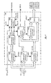
- FIG. 3 illustrates, as an example, a block diagram of an EEPROM system 4000 formed on an EEPROM chip and including a plurality of flash EEPROM cells 400 organized into four subarrays or quadrants, 400 - 0 to 400 - 3 .
- each subarray or quadrant comprises up to 16K addressable rows of up to 16 addressable data chunks.
- Each data chunk includes a plurality of bits, such as 64 bits, which are communicated as an addressable unit to the EEPROM system 4000 via a 2-bit wide serial input bus SI( 0 : 1 ) 411 , or from the EEPROM system 4000 via a 2-bit wide serial output bus SO( 0 : 1 ) 414 .
- Each flash EEPROM cell may also include a plurality of bits, such as 2 or 4, if multi-state memory cells are employed.
- a left row decoder (X-DEC) 401 decodes row addresses for quadrants 400 - 0 and 400 - 1 , which share the left row decoder 401 by sharing word lines
- a right row decoder (X-DEC) 406 decodes row addresses for quadrants 400 - 2 and 400 - 3 , which share the right row decoder 406 by also sharing word lines.
- the left row decoder 401 receives row addresses via left internal row address lines AXL( 0 : 13 ) from a write control logic circuit 450 to decode up to 16K rows
- the right row decoder 406 receives row addresses via right internal row address lines AXR( 0 : 13 ) from the write control logic circuit 450 to also decode up to 16K rows.
- First, second, third, and fourth column decoder and sense amplifier circuits (Y-DEC) 402 , 403 , 407 , and 408 are respectively coupled to first, second, third, and fourth quadrants 400 -D, 400 - 1 , 400 - 2 , and 400 - 3 to decode column chunk addresses, and transmit data to and from locations corresponding to the column chunk addresses and row addresses received by their respective row decoders.
- Y-DEC column decoder and sense amplifier circuits
- the first column decoder and sense amplifier circuit 402 receives column chunk addresses via first left internal column address lines AYL 1 ( 0 : 3 ) from the write control logic circuit 450 to decode up to 16 chunk columns
- the second column decoder and sense amplifier circuit 403 receives column chunk addresses via second left internal column address lines AYL 2 ( 0 : 3 ) from the write control logic circuit 450 to decode up to 16 chunk columns
- the third column decoder and sense amplifier circuit 407 receives column chunk addresses via first right internal column address lines AYR 1 ( 0 : 3 ) from the write control logic circuit 450 to decode up to 16 chunk columns
- the fourth column decoder and sense amplifier circuit 408 receives column chunk addresses via second right internal column address lines AYR 2 ( 0 : 3 ) from the write control logic circuit 450 to decode up to 16 chunk columns.
- First, second, third, and fourth data registers (DATA REG.) 404 , 405 , 409 , and 410 are each coupled to the serial input bus 411 and the serial output bus 414 , and respectively coupled to the first, second, third, and fourth column decoder and sense amplifier circuits 402 , 403 , 407 , and 408 respectively through first, second, third, and fourth program/verify circuits 454 , 455 , 459 , and 460 .
- Each of the data registers 404 , 405 , 409 , and 410 stores up to a chunk of data which is to be programmed into or is read from their respective quadrants.
- the chunks of data are first sequentially latched into the data registers 404 , 405 , 409 , and 410 , in response to latch enable signals Q( 0 ), Q( 1 ), Q( 2 ), and Q( 3 ) provided by the write control logic circuit 450 , and control signals CS provided, for example, by a serial protocol logic circuit (not shown) included in an EEPROM device along with the EEPROM system 4000 .
- the control signals CS include, as examples, a read/program signal which indicates whether data is being read from or written to the quadrants 400 - 0 to 400 - 3 , a program data signal (PDAT) which indicates that a chunk of data is ready to be received via the serial input bus 411 , and a clock signal for serially loading the data from the serial input bus 411 into an enabled one of the first, second, third, and fourth data registers 404 , 405 , 409 , and 410 .
- a read/program signal which indicates whether data is being read from or written to the quadrants 400 - 0 to 400 - 3
- PDAT program data signal
- a clock signal for serially loading the data from the serial input bus 411 into an enabled one of the first, second, third, and fourth data registers 404 , 405 , 409 , and 410 .
- programming and verifying the programming of the latched data is performed under the control of the program/verify circuits 454 , 455 , 459 , and 460 in response to activation of program enable lines PGM( 0 ), PGM( 1 ), PGM( 2 ), and PGM( 3 ) provided by the write control logic circuit 450 , so that a series of program/verify steps are performed until all bits of the data chunks being programmed and verified in parallel are programmed and verified as having been programmed correctly.
- the write control logic circuit 450 is coupled to the serial input bus SI( 0 : 1 ) 411 , control signal line PD 412 , and multi-chunk program line MS 413 to activate program enable lines PGM( 0 : 3 ) for column decoder and sense amplifier circuits 402 , 403 , 407 , and 408 , data register enable signals Q( 0 : 3 ) for data registers 404 , 405 , 409 , and 410 , first and second right internal column address lines, AYR 1 ( 0 : 3 ) and AYR 2 ( 0 : 3 ), for column decoder and sense amplifier circuits, 407 and 408 , first and second left internal column address lines, AYL 1 ( 0 : 3 ) and AYL 2 ( 0 : 3 ), for column decoder and sense amplifier circuits, 402 and 403 , and left and right internal row address lines, AXL( 0 : 13 ) and AXR( 0
- serial protocol logic link such as employed in communicating with the EEPROM system 4000
- U.S. Pat. No. 5,430,859 which is incorporated herein by this reference
- flash EEPROM device employing a serial protocol link to communicate with the flash EEPROM device.
- program/verify circuits such as program/verify circuits 454 , 455 , 459 , and 460
- U.S. Pat. No. 5,172,338 which is incorporated herein by this reference, and describes certain write circuits and techniques for programming a chunk of data at a time into a flash EEPROM device.
- FIGS. 4 and 5 respectively illustrate, as examples, a block diagram detailing the structure of the write control logic circuit 450 , and timing diagrams useful for describing the operation of the write control logic circuit 450 .
- a register enable circuit 510 has inputs coupled to the serial input bus 411 and to the control signal line PD 412 , and outputs coupled to an address register 501 , command register 502 , and latch enable circuit 505 of the write control logic circuit 450 .
- the register enable circuit 510 first receives the serial protocol operator 201 - 1 having the bit code “10” which indicates that a command follows.
- the register enable circuit 510 activates an enable line PCMD at a falling edge 211 of the control signal line PD 412 , which causes a multi-chunk write command 201 - 2 following the serial protocol operator 201 - 1 on the serial input bus SI( 0 : 1 ) 411 to be latched into a command register 502 at time t 1 .
- a command decoder 504 coupled to the command register 502 thereupon reads the command stored therein and decodes it to activate, in this case, the multi-chunk write line MULT to indicate that a multi-chunk write operation follows.
- the multi-chunk write line MULT thereupon remains active throughout the multi-chunk write operation.
- the register enable circuit 510 next receives the serial protocol operator 202 - 1 having the bit code “01” which indicates that a chunk address follows. In response, the register enable circuit 510 activates an enable line PADR at a falling edge 212 of the control signal line PD 412 , which causes a chunk address 202 - 2 following the serial protocol operator 202 - 1 on the serial input bus SI( 0 : 1 ) 411 to be latched into an address register 501 at time t 2 .
- the chunk address stored in the address latches 503 are then provided over appropriate lines of internal row address lines, AXL( 0 : 13 ) and AXR( 0 : 13 ), to row decoders, 401 and 406 , and internal column address lines, AYL 1 ( 0 : 3 ), AYL 2 ( 0 : 3 ), AYR 1 ( 0 : 3 ), and AYR 2 ( 0 : 3 ), to column decoder and sense amplifier circuits 402 , 403 , 407 , and 408 .
- the register enable circuit 510 next receives the serial protocol operator 202 - 3 having the bit code “11” which indicates that a chunk of data follows. In response, the register enable circuit 510 activates an enable line PDAT at a falling edge 213 of the control signal line PD 412 , which causes a chunk of data 202 - 4 following the serial protocol operator 202 - 3 on the serial input bus SI( 0 : 1 ) 411 to be latched into an appropriate one of the data registers 404 , 405 , 409 , and 410 at time t 3 .
- the latch enable circuit 505 determines the data register in which the chunk of data is to be stored from the two most-significant-bits A( 18 ), A( 17 ) of the chunk address stored in the address register 501 , and activates the appropriate one of the data latch enable signals Q( 0 : 3 ) upon activation of the enable line PDAT.
- the data latch enable signal Q( 0 ) may be activated to latch the data into data register 404 ; if address bit A( 18 ) is “0” and A( 17 ) is “1”, then the data latch enable signal Q( 1 ) may be activated to latch the data into data register 405 ; if address bit A( 18 ) is “1” and A( 17 ) is “0”, then the data latch enable signal Q( 2 ) may be activated to latch the data into data register 409 ; and if both address bits A( 18 ) and A( 17 ) are “1”, then the data latch enable signal Q( 3 ) may be activated to latch the data into data register 410 .
- address bit A( 18 ) indicates whether the data chunk is to be programmed into a left plane comprising quandrants 400 - 0 and 400 - 1 which share row decoder 401 , or a right plane comprising quadrants 400 - 2 and 400 - 3 which share row decoder 406 ; and address bit A( 17 ) indicates whether the data chunk is to be programmed into a left or right quadrant in that plane.
- the register enable circuit 510 next receives address and data information for subsequent data chunks to be concurrently programmed into different ones of the quadrants 400 - 0 to 400 - 3 , and causes them to be handled in the same fashion as the first chunk address 202 - 2 and first data chunk 202 - 4 .
- the first data chunk 202 - 4 may be latched into the first data register 404 to be programmed into the first quadrant 400 - 0
- a second data chunk 203 - 4 may be latched into the second data register 405 to be programmed into the second quadrant 400 - 1
- a third data chunk 204 - 4 may be latched into the third data register 409 to be programmed into the third quadrant 400 - 2
- a fourth data chunk 205 - 4 may be latched into the fourth data register 410 to be programmed into the fourth quadrant 400 - 3 .
- the register enable circuit 510 then receives the serial protocol operator 206 - 1 having the bit code “10” which indicates that a command follows. In response, the register enable circuit 510 activates an enable line PCMD at a falling edge 216 of the control signal line PD 412 , which causes a program command 206 - 2 following the serial protocol operator 206 - 1 on the serial input bus SI( 0 : 1 ) 411 to be latched into the command register 502 at time t 6 .
- the command decoder 504 thereupon reads the command stored therein and decodes it to activate, in this case, a program line PGM.
- a program enable circuit 506 receives the program line PGM, the multi-chunk program line MS 413 , and the most-significant-bit A( 18 ) from the chunk address stored in the address register 501 and activates in response thereof, the program enable lines PGM( 0 ), PGM( 1 ), PGM( 2 ), and PGM( 3 ) provided to the program/verify circuits 454 , 455 , 459 , and 460 to selectively activate their respective program/verify modes of operation.
- FIG. 6 illustrates, as an example, a block diagram further detailing the address latches 503 , the latch enable circuit 505 , and a multiplexer circuit 515 of the write control logic 450 .
- the address latches 503 include first and second row address latches, 503 - 1 and 503 - 2 , for storing row addresses to be decoded respectively by the left and right row decoders, 401 and 406 , and first, second, third, and fourth column address latches, 503 - 3 , 503 - 4 , 503 - 5 , and 503 - 6 , for storing column addresses to be decoded respectively by the first, second, third, and fourth column decoder and sense amplifier circuits, 402 , 403 , 407 , and 408 .
- the first and second row address latches, 503 - 1 and 503 - 2 are coupled to address bits A( 4 : 17 ) so that when the first row address latch 503 - 1 is enabled by activating enable line X(L), the first row address latch 503 - 1 latches these bits into its contents, and when the second row address latch 503 - 2 is enabled by activating enable line X(R), the second row address latch 503 - 2 latches these bits into its contents.
- the first, second, third, and fourth column latches, 503 - 3 to 503 - 6 are coupled to address bits A( 0 : 3 ) of the address register 501 so that when the first column latch 503 - 3 is enabled by activating enable line Y(L 1 ), the first column latch 503 - 3 latches these bits into its contents, when the second column latch 503 - 4 is enabled by activating enable line Y(L 2 ), the second column latch 503 - 4 latches these bits into its contents, when the third column latch 503 - 5 is enabled by activating enable line Y(R 1 ), the third column latch 503 - 5 latches these bits into its contents, and when the fourth column latch 503 - 6 is enabled by activating enable line Y(R 2 ), the fourth column latch 503 - 6 latches these bits into its contents.
- the multiplexer circuit 515 includes six multiplexers, 515 - 1 to 515 - 6 .
- the multiplexers 515 - 1 and 515 - 2 respectively generate the left and right row address lines AXL( 0 : 13 ) and AXR( 0 : 13 ) provided to the left and right row decoders 401 and 406
- the multiplexers 515 - 3 to 515 - 6 respectively generate the column address lines AYL 1 ( 0 : 3 ), AYL 2 ( 0 : 3 ), AYR 1 ( 0 : 3 ), and AYR 2 ( 0 : 3 ) provided to the column decoder and sense amplifier circuits 402 , 403 , 407 , and 408 .
- Each of the multiplexers 515 - 1 and 515 - 2 has a first set of inputs coupled to address bits A( 4 : 17 ) of the address-register 501 , a second set of inputs coupled to a corresponding one of the row address latches 503 - 1 and 503 - 2 , and a select input coupled to the multi-chunk write line MULT generated by the command decoder 504 , wherein address bits A( 4 : 17 ) indicate a quadrant row address.
- each of the multiplexers 515 - 3 to 515 - 6 has a first set of inputs coupled to address bits A( 0 : 3 ) of the address register 501 , a second set of inputs coupled to a corresponding one of the column address latches 503 - 3 to 503 - 6 , and a select input coupled to the multi-chunk write line MULT generated by the command decoder 504 , wherein address bits A( 0 : 3 ) indicate a quadrant column address.
- the multi-chunk write line MULT is activated, and the six multiplexers, 515 - 1 to 515 - 6 , pass their second set of inputs, i.e., the row and column addresses previously latched into their corresponding row and column address latches, 503 - 1 to 503 - 6 , to their respective row and column decoders via address lines, AXL( 0 : 13 ), AXR( 0 : 13 ), AYL 1 ( 0 : 3 ), AYL 2 ( 0 : 3 ), AYR 1 ( 0 : 3 ), and AYR 2 ( 0 : 3 ).
- the multi-chunk write line MULT is not activated, and the six multiplexers, 515 - 1 to 515 - 6 , pass their first set of inputs, i.e., the row and column addresses indicated by bits A( 4 : 17 ) and A( 0 : 3 ) stored in the address register 501 , to their respective row and column decoders via address lines, AXL( 0 : 13 ), AXR( 0 : 13 ), AYL 1 ( 0 : 3 ), AYL 2 ( 0 : 3 ), AYR 1 ( 0 : 3 ), and AYR 2 ( 0 : 3 ).
- the latch enable circuit 505 includes a quadrant decoder circuit 505 - 1 , an address latch control generator circuit 505 - 2 , and an AND logic circuit 505 - 3 .
- the quadrant decoder circuit 505 - 1 receives the address bits A( 18 ) and A( 17 ) from the address register 501 , and activates one of four internal quadrant lines Q( 0 : 3 )′.
- the address latch control generator circuit 505 - 2 receives the address bit A( 18 ) from the address register 501 , the enable line PDAT from the register enable circuit 510 , the multi-chunk write line MULT from the command decoder 504 , and the internal quadrant lines Q( 0 : 3 )′ from the quadrant decoder circuit 505 - 1 , and activates appropriate ones of the latch enable lines X(L), X(R), Y(L 1 ), Y(L 2 ), Y(R 1 ), and Y(R 2 ) provided to the row and column address latches, 503 - 1 to 503 - 6 .
- the AND logic circuit 505 - 3 receives the internal quadrant lines Q( 0 : 3 )′ from the quadrant decoder circuit 505 - 1 and the enable line PDAT from the register enable circuit 510 , and activates appropriate ones of the data latch enable lines Q( 0 : 3 ) in such a fashion that the data latch enable line Q( 0 ) is only active if the internal quadrant line Q( 0 )′ and the enable line PDAT are both active, the data latch enable line Q( 1 ) is only active if the internal quadrant line Q( 1 )′ and the enable line PDAT are both active, the data latch enable line Q( 2 ) is only active if the internal quadrant line Q( 2 )′ and the enable line PDAT are both active, and the data latch enable line Q( 0 ) is only active if the internal quadrant line Q( 0 )′ and the enable line PDAT are both active.
- FIG. 7 illustrates, as an example, a logic diagram of the quadrant decoder 505 - 1 .
- the quadrant decoder 505 - 1 includes four NAND gates 701 to 704 , and six inverters 705 to 710 .
- the inverter 705 has an input coupled to the address bit A( 18 ) of the address register 501 , and an output coupled to first inputs of the NAND gates 701 and 702 .
- the inverter 706 has an input coupled to the address bit A( 17 ) of the address register 501 , and an output coupled to second inputs of the NAND gates 701 and 703 .
- the address bit A( 18 ) is directly coupled to first inputs of the NAND gates 703 and 704
- the address bit A( 17 ) is directly coupled to second inputs of the NAND gates 702 and 704
- the inverters 707 to 710 have inputs respectively coupled to corresponding outputs of the NAND gates 701 to 704 , and outputs respectively providing the four internal quadrant lines Q( 0 : 3 )′.
- the internal quadrant line Q( 0 )′ corresponding to the quadrant 400 - 0 and data register 404 is activated
- the internal quadrant line Q( 1 )′ corresponding to the quadrant 400 - 1 and data register 405 is activated
- the internal quadrant line Q( 2 )′ corresponding to the quadrant 400 - 2 and data register 409 is activated
- the address bits A( 18 ) and A( 17 ) are both “1”
- the internal quadrant line Q( 3 )′ corresponding to the quadrant 400 - 3 and data register 410 is activated.
- FIG. 8 illustrates, as an example, a logic diagram of the address latch control generator 505 - 2 . Included in the address latch control generator 505 - 2 are six NAND gates, 801 to 806 , and seven inverters, 807 to 813 . Each of the six NAND gates, 801 to 806 , has a first input coupled to the enable line PDAT provided by the register enable circuit 510 , and a second input coupled to the multi-chunk write line MULT provided by the command decoder circuit 504 .
- the inverters 808 to 813 have inputs respectively coupled to corresponding outputs of the NAND gates 801 to 806 , and outputs activating appropriate ones of the row and column latch enable lines X(R), X(L), Y(L 1 ), Y(L 2 ), Y(R 1 ), and Y(R 2 ). Accordingly, the row and column latch enable lines X(R), X(L), Y(L 1 ), Y(L 2 ), Y(R 1 ), and Y(R 2 ) are only activated during a multi-chunk write operation, i.e., while the multi-chunk write line MULT is activated, and while the enable line PDAT is activated.
- one or the other of the latch enable lines X(L) and X(R) is activated, depending upon which plane corresponds to the address stored in the address register 501
- one of the latch enable lines Y(L 1 ), Y(L 2 ), Y(R 1 ), and Y(R 2 ) is activated, depending upon which quadrant corresponds to the address stored in the address register 501 .
- the activated left and right plane lines, LEFT and RIGHT, thereupon remain activated until a reset line R provided to a reset input of the left/right select switch circuit 901 is activated.
- the quad latch circuit 902 receives the left and right plane lines, LEFT and RIGHT, from the left/right select switch circuit 901 , the internal row address lines AXL( 13 ) and AXR( 13 ) from the multiplexers 515 - 1 and 515 - 2 , and the multi-chunk write line MULT from the command decoder circuit 504 , and activates appropriate ones of quadrant latch lines QL( 0 : 3 ) such that the quadrant latch line QL( 0 ) is activated if data is to be programmed into the quadrant 400 - 0 during the multi-chunk write operation, the quadrant latch line QL( 1 ) is activated if data is to be programmed into the quadrant 400 - 1 during the multi-chunk write operation, the quadrant
- the AND logic circuit 903 receives the quadrant latch lines QL( 0 : 3 ) from the quad latch circuit 902 , the enable line PGM from the command decoder circuit 504 , and the multi-chunk program line 413 provided, for example, by a microprocessor (not shown) or controller (not shown) which communicates with the EEPROM system 4000 through the serial input and output lines, 411 and 414 , and control signal lines, 412 and 413 , and activates appropriate ones of the program enable lines PGM( 0 ), PGM( 1 ), PGM( 2 ), and PGM( 3 ) such that program enable line PGM( 0 ) is activated only if data is to be programmed into quadrant 400 - 0 and both the program enable line PGM and the multi-chunk program line are active, program enable line PGM(L) is activated only if data is to be programmed into quadrant 400 - 1 and both the program enable line PGM and the multi-chunk program line are active, program enable line P
Abstract
Description
Claims (12)
Priority Applications (1)
| Application Number | Priority Date | Filing Date | Title |
|---|---|---|---|
| US12/469,531 US7890694B2 (en) | 1996-11-05 | 2009-05-20 | Latched address multi-chunk write to EEPROM |
Applications Claiming Priority (6)
| Application Number | Priority Date | Filing Date | Title |
|---|---|---|---|
| US08/743,857 US5890192A (en) | 1996-11-05 | 1996-11-05 | Concurrent write of multiple chunks of data into multiple subarrays of flash EEPROM |
| US09/226,405 US6157983A (en) | 1996-11-05 | 1999-01-06 | Concurrent write of multiple chunks of data into multiple subarrays of flash EEPROM |
| US09/642,880 US6542956B1 (en) | 1996-11-05 | 2000-08-21 | Latched address multi-chunk write to EEPROM |
| US10/286,078 US6829673B2 (en) | 1996-11-05 | 2002-11-01 | Latched address multi-chunk write to EEPROM |
| US10/447,134 US20030200380A1 (en) | 1996-11-05 | 2003-05-27 | Latched address multi-chunk write to EEPROM |
| US12/469,531 US7890694B2 (en) | 1996-11-05 | 2009-05-20 | Latched address multi-chunk write to EEPROM |
Related Parent Applications (1)
| Application Number | Title | Priority Date | Filing Date |
|---|---|---|---|
| US10/447,134 Continuation US20030200380A1 (en) | 1996-11-05 | 2003-05-27 | Latched address multi-chunk write to EEPROM |
Publications (2)
| Publication Number | Publication Date |
|---|---|
| US20090228644A1 US20090228644A1 (en) | 2009-09-10 |
| US7890694B2 true US7890694B2 (en) | 2011-02-15 |
Family
ID=24990480
Family Applications (6)
| Application Number | Title | Priority Date | Filing Date |
|---|---|---|---|
| US08/743,857 Expired - Lifetime US5890192A (en) | 1996-11-05 | 1996-11-05 | Concurrent write of multiple chunks of data into multiple subarrays of flash EEPROM |
| US09/226,405 Expired - Fee Related US6157983A (en) | 1996-11-05 | 1999-01-06 | Concurrent write of multiple chunks of data into multiple subarrays of flash EEPROM |
| US09/642,880 Expired - Lifetime US6542956B1 (en) | 1996-11-05 | 2000-08-21 | Latched address multi-chunk write to EEPROM |
| US10/286,078 Expired - Fee Related US6829673B2 (en) | 1996-11-05 | 2002-11-01 | Latched address multi-chunk write to EEPROM |
| US10/447,134 Abandoned US20030200380A1 (en) | 1996-11-05 | 2003-05-27 | Latched address multi-chunk write to EEPROM |
| US12/469,531 Expired - Fee Related US7890694B2 (en) | 1996-11-05 | 2009-05-20 | Latched address multi-chunk write to EEPROM |
Family Applications Before (5)
| Application Number | Title | Priority Date | Filing Date |
|---|---|---|---|
| US08/743,857 Expired - Lifetime US5890192A (en) | 1996-11-05 | 1996-11-05 | Concurrent write of multiple chunks of data into multiple subarrays of flash EEPROM |
| US09/226,405 Expired - Fee Related US6157983A (en) | 1996-11-05 | 1999-01-06 | Concurrent write of multiple chunks of data into multiple subarrays of flash EEPROM |
| US09/642,880 Expired - Lifetime US6542956B1 (en) | 1996-11-05 | 2000-08-21 | Latched address multi-chunk write to EEPROM |
| US10/286,078 Expired - Fee Related US6829673B2 (en) | 1996-11-05 | 2002-11-01 | Latched address multi-chunk write to EEPROM |
| US10/447,134 Abandoned US20030200380A1 (en) | 1996-11-05 | 2003-05-27 | Latched address multi-chunk write to EEPROM |
Country Status (1)
| Country | Link |
|---|---|
| US (6) | US5890192A (en) |
Families Citing this family (240)
| Publication number | Priority date | Publication date | Assignee | Title |
|---|---|---|---|---|
| US5657332A (en) * | 1992-05-20 | 1997-08-12 | Sandisk Corporation | Soft errors handling in EEPROM devices |
| US6978342B1 (en) | 1995-07-31 | 2005-12-20 | Lexar Media, Inc. | Moving sectors within a block of information in a flash memory mass storage architecture |
| US5845313A (en) * | 1995-07-31 | 1998-12-01 | Lexar | Direct logical block addressing flash memory mass storage architecture |
| US6757800B1 (en) | 1995-07-31 | 2004-06-29 | Lexar Media, Inc. | Increasing the memory performance of flash memory devices by writing sectors simultaneously to multiple flash memory devices |
| US8171203B2 (en) * | 1995-07-31 | 2012-05-01 | Micron Technology, Inc. | Faster write operations to nonvolatile memory using FSInfo sector manipulation |
| US6801979B1 (en) | 1995-07-31 | 2004-10-05 | Lexar Media, Inc. | Method and apparatus for memory control circuit |
| US6728851B1 (en) | 1995-07-31 | 2004-04-27 | Lexar Media, Inc. | Increasing the memory performance of flash memory devices by writing sectors simultaneously to multiple flash memory devices |
| US6081878A (en) * | 1997-03-31 | 2000-06-27 | Lexar Media, Inc. | Increasing the memory performance of flash memory devices by writing sectors simultaneously to multiple flash memory devices |
| US6411546B1 (en) | 1997-03-31 | 2002-06-25 | Lexar Media, Inc. | Nonvolatile memory using flexible erasing methods and method and system for using same |
| US6275894B1 (en) * | 1998-09-23 | 2001-08-14 | Advanced Micro Devices, Inc. | Bank selector circuit for a simultaneous operation flash memory device with a flexible bank partition architecture |
| KR100544175B1 (en) * | 1999-05-08 | 2006-01-23 | 삼성전자주식회사 | Recording medium storing linking type information and method for processing defective area |
| JP4023953B2 (en) * | 1999-06-22 | 2007-12-19 | 株式会社ルネサステクノロジ | Nonvolatile semiconductor memory device |
| JP2001167586A (en) * | 1999-12-08 | 2001-06-22 | Toshiba Corp | Non-volatile semiconductor memory |
| US6851013B1 (en) * | 1999-12-15 | 2005-02-01 | Intel Corporation | Fast program mode |
| US6426893B1 (en) | 2000-02-17 | 2002-07-30 | Sandisk Corporation | Flash eeprom system with simultaneous multiple data sector programming and storage of physical block characteristics in other designated blocks |
| US6950336B2 (en) * | 2000-05-03 | 2005-09-27 | Emosyn America, Inc. | Method and apparatus for emulating an electrically erasable programmable read only memory (EEPROM) using non-volatile floating gate memory cells |
| US6400603B1 (en) | 2000-05-03 | 2002-06-04 | Advanced Technology Materials, Inc. | Electronically-eraseable programmable read-only memory having reduced-page-size program and erase |
| US7167944B1 (en) | 2000-07-21 | 2007-01-23 | Lexar Media, Inc. | Block management for mass storage |
| US6567307B1 (en) | 2000-07-21 | 2003-05-20 | Lexar Media, Inc. | Block management for mass storage |
| US6266273B1 (en) | 2000-08-21 | 2001-07-24 | Sandisk Corporation | Method and structure for reliable data copy operation for non-volatile memories |
| US6570785B1 (en) | 2000-10-31 | 2003-05-27 | Sandisk Corporation | Method of reducing disturbs in non-volatile memory |
| US6717851B2 (en) * | 2000-10-31 | 2004-04-06 | Sandisk Corporation | Method of reducing disturbs in non-volatile memory |
| US6684289B1 (en) | 2000-11-22 | 2004-01-27 | Sandisk Corporation | Techniques for operating non-volatile memory systems with data sectors having different sizes than the sizes of the pages and/or blocks of the memory |
| US7020739B2 (en) * | 2000-12-06 | 2006-03-28 | Tdk Corporation | Memory controller, flash memory system having memory controller and method for controlling flash memory device |
| US7020736B1 (en) * | 2000-12-18 | 2006-03-28 | Redback Networks Inc. | Method and apparatus for sharing memory space across mutliple processing units |
| US6661730B1 (en) | 2000-12-22 | 2003-12-09 | Matrix Semiconductor, Inc. | Partial selection of passive element memory cell sub-arrays for write operation |
| US6763424B2 (en) * | 2001-01-19 | 2004-07-13 | Sandisk Corporation | Partial block data programming and reading operations in a non-volatile memory |
| JP2002318666A (en) * | 2001-04-20 | 2002-10-31 | Hitachi Ltd | Update method of firmware of hard disk unit mounted on disk array device and disk array device with function for performing the updating method |
| US6522580B2 (en) | 2001-06-27 | 2003-02-18 | Sandisk Corporation | Operating techniques for reducing effects of coupling between storage elements of a non-volatile memory operated in multiple data states |
| JP2003036681A (en) * | 2001-07-23 | 2003-02-07 | Hitachi Ltd | Non-volatile memory device |
| US7554842B2 (en) * | 2001-09-17 | 2009-06-30 | Sandisk Corporation | Multi-purpose non-volatile memory card |
| US7170802B2 (en) * | 2003-12-31 | 2007-01-30 | Sandisk Corporation | Flexible and area efficient column redundancy for non-volatile memories |
| US6456528B1 (en) | 2001-09-17 | 2002-09-24 | Sandisk Corporation | Selective operation of a multi-state non-volatile memory system in a binary mode |
| US6717847B2 (en) * | 2001-09-17 | 2004-04-06 | Sandisk Corporation | Selective operation of a multi-state non-volatile memory system in a binary mode |
| US6985388B2 (en) * | 2001-09-17 | 2006-01-10 | Sandisk Corporation | Dynamic column block selection |
| GB0123410D0 (en) | 2001-09-28 | 2001-11-21 | Memquest Ltd | Memory system for data storage and retrieval |
| GB0123415D0 (en) * | 2001-09-28 | 2001-11-21 | Memquest Ltd | Method of writing data to non-volatile memory |
| GB0123417D0 (en) * | 2001-09-28 | 2001-11-21 | Memquest Ltd | Improved data processing |
| GB0123416D0 (en) * | 2001-09-28 | 2001-11-21 | Memquest Ltd | Non-volatile memory control |
| GB0123421D0 (en) * | 2001-09-28 | 2001-11-21 | Memquest Ltd | Power management system |
| US6967872B2 (en) | 2001-12-18 | 2005-11-22 | Sandisk Corporation | Method and system for programming and inhibiting multi-level, non-volatile memory cells |
| JP4061272B2 (en) * | 2002-01-09 | 2008-03-12 | 株式会社ルネサステクノロジ | Memory system and memory card |
| US7246268B2 (en) * | 2002-01-16 | 2007-07-17 | Sandisk Corporation | Method and apparatus for dynamic degradation detection |
| US6621739B2 (en) * | 2002-01-18 | 2003-09-16 | Sandisk Corporation | Reducing the effects of noise in non-volatile memories through multiple reads |
| US6542407B1 (en) * | 2002-01-18 | 2003-04-01 | Sandisk Corporation | Techniques of recovering data from memory cells affected by field coupling with adjacent memory cells |
| US7231643B1 (en) | 2002-02-22 | 2007-06-12 | Lexar Media, Inc. | Image rescue system including direct communication between an application program and a device driver |
| US6871257B2 (en) | 2002-02-22 | 2005-03-22 | Sandisk Corporation | Pipelined parallel programming operation in a non-volatile memory system |
| US6751129B1 (en) * | 2002-05-21 | 2004-06-15 | Sandisk Corporation | Efficient read, write methods for multi-state memory |
| US6781877B2 (en) * | 2002-09-06 | 2004-08-24 | Sandisk Corporation | Techniques for reducing effects of coupling between storage elements of adjacent rows of memory cells |
| WO2004040586A1 (en) * | 2002-10-28 | 2004-05-13 | Sandisk Corporation | Automated wear leveling in non-volatile storage systems |
| US6901498B2 (en) * | 2002-12-09 | 2005-05-31 | Sandisk Corporation | Zone boundary adjustment for defects in non-volatile memories |
| US7069377B2 (en) * | 2003-05-08 | 2006-06-27 | Micron Technology, Inc. | Scratch control memory array in a flash memory device |
| US7046555B2 (en) | 2003-09-17 | 2006-05-16 | Sandisk Corporation | Methods for identifying non-volatile memory elements with poor subthreshold slope or weak transconductance |
| US7173852B2 (en) | 2003-10-03 | 2007-02-06 | Sandisk Corporation | Corrected data storage and handling methods |
| US7012835B2 (en) * | 2003-10-03 | 2006-03-14 | Sandisk Corporation | Flash memory data correction and scrub techniques |
| US8504798B2 (en) * | 2003-12-30 | 2013-08-06 | Sandisk Technologies Inc. | Management of non-volatile memory systems having large erase blocks |
| US7631138B2 (en) * | 2003-12-30 | 2009-12-08 | Sandisk Corporation | Adaptive mode switching of flash memory address mapping based on host usage characteristics |
| US7383375B2 (en) | 2003-12-30 | 2008-06-03 | Sandisk Corporation | Data run programming |
| US7139864B2 (en) * | 2003-12-30 | 2006-11-21 | Sandisk Corporation | Non-volatile memory and method with block management system |
| US7173863B2 (en) * | 2004-03-08 | 2007-02-06 | Sandisk Corporation | Flash controller cache architecture |
| US7433993B2 (en) * | 2003-12-30 | 2008-10-07 | San Disk Corportion | Adaptive metablocks |
| US20050144363A1 (en) * | 2003-12-30 | 2005-06-30 | Sinclair Alan W. | Data boundary management |
| US8250295B2 (en) | 2004-01-05 | 2012-08-21 | Smart Modular Technologies, Inc. | Multi-rank memory module that emulates a memory module having a different number of ranks |
| US20080228996A1 (en) * | 2004-01-20 | 2008-09-18 | Trek 2000 International Ltd. | Portable Data Storage Device Using Multiple Memory Devices |
| US7154779B2 (en) * | 2004-01-21 | 2006-12-26 | Sandisk Corporation | Non-volatile memory cell using high-k material inter-gate programming |
| US7127549B2 (en) | 2004-02-04 | 2006-10-24 | Sandisk Corporation | Disk acceleration using first and second storage devices |
| US7136973B2 (en) * | 2004-02-04 | 2006-11-14 | Sandisk Corporation | Dual media storage device |
| US7355237B2 (en) * | 2004-02-13 | 2008-04-08 | Sandisk Corporation | Shield plate for limiting cross coupling between floating gates |
| EP2506486A1 (en) * | 2004-02-23 | 2012-10-03 | Lexar Media, Inc. | Secure compact flash |
| KR20050087719A (en) * | 2004-02-26 | 2005-08-31 | 오끼 덴끼 고오교 가부시끼가이샤 | Semiconductor memory device |
| US7725628B1 (en) | 2004-04-20 | 2010-05-25 | Lexar Media, Inc. | Direct secondary device interface by a host |
| US7370166B1 (en) | 2004-04-30 | 2008-05-06 | Lexar Media, Inc. | Secure portable storage device |
| US7023733B2 (en) * | 2004-05-05 | 2006-04-04 | Sandisk Corporation | Boosting to control programming of non-volatile memory |
| US7490283B2 (en) | 2004-05-13 | 2009-02-10 | Sandisk Corporation | Pipelined data relocation and improved chip architectures |
| US8429313B2 (en) * | 2004-05-27 | 2013-04-23 | Sandisk Technologies Inc. | Configurable ready/busy control |
| US8607016B2 (en) * | 2004-07-21 | 2013-12-10 | Sandisk Technologies Inc. | FAT analysis for optimized sequential cluster management |
| US7395384B2 (en) | 2004-07-21 | 2008-07-01 | Sandisk Corproation | Method and apparatus for maintaining data on non-volatile memory systems |
| US8375146B2 (en) * | 2004-08-09 | 2013-02-12 | SanDisk Technologies, Inc. | Ring bus structure and its use in flash memory systems |
| US7594063B1 (en) * | 2004-08-27 | 2009-09-22 | Lexar Media, Inc. | Storage capacity status |
| US7464306B1 (en) * | 2004-08-27 | 2008-12-09 | Lexar Media, Inc. | Status of overall health of nonvolatile memory |
| US20060069896A1 (en) * | 2004-09-27 | 2006-03-30 | Sigmatel, Inc. | System and method for storing data |
| US7441067B2 (en) | 2004-11-15 | 2008-10-21 | Sandisk Corporation | Cyclic flash memory wear leveling |
| US7120051B2 (en) * | 2004-12-14 | 2006-10-10 | Sandisk Corporation | Pipelined programming of non-volatile memories using early data |
| US7420847B2 (en) * | 2004-12-14 | 2008-09-02 | Sandisk Corporation | Multi-state memory having data recovery after program fail |
| US7366826B2 (en) * | 2004-12-16 | 2008-04-29 | Sandisk Corporation | Non-volatile memory and method with multi-stream update tracking |
| US7412560B2 (en) * | 2004-12-16 | 2008-08-12 | Sandisk Corporation | Non-volatile memory and method with multi-stream updating |
| US7315916B2 (en) * | 2004-12-16 | 2008-01-01 | Sandisk Corporation | Scratch pad block |
| US7386655B2 (en) * | 2004-12-16 | 2008-06-10 | Sandisk Corporation | Non-volatile memory and method with improved indexing for scratch pad and update blocks |
| US7395404B2 (en) | 2004-12-16 | 2008-07-01 | Sandisk Corporation | Cluster auto-alignment for storing addressable data packets in a non-volatile memory array |
| KR100684887B1 (en) * | 2005-02-04 | 2007-02-20 | 삼성전자주식회사 | Data storing device including flash memory and merge method of thereof |
| US7849381B2 (en) * | 2004-12-21 | 2010-12-07 | Sandisk Corporation | Method for copying data in reprogrammable non-volatile memory |
| US20090172269A1 (en) * | 2005-02-04 | 2009-07-02 | Samsung Electronics Co., Ltd. | Nonvolatile memory device and associated data merge method |
| US8122193B2 (en) * | 2004-12-21 | 2012-02-21 | Samsung Electronics Co., Ltd. | Storage device and user device including the same |
| US7409473B2 (en) | 2004-12-21 | 2008-08-05 | Sandisk Corporation | Off-chip data relocation |
| US7882299B2 (en) * | 2004-12-21 | 2011-02-01 | Sandisk Corporation | System and method for use of on-chip non-volatile memory write cache |
| US7212440B2 (en) * | 2004-12-30 | 2007-05-01 | Sandisk Corporation | On-chip data grouping and alignment |
| US20060161724A1 (en) * | 2005-01-20 | 2006-07-20 | Bennett Alan D | Scheduling of housekeeping operations in flash memory systems |
| US7315917B2 (en) * | 2005-01-20 | 2008-01-01 | Sandisk Corporation | Scheduling of housekeeping operations in flash memory systems |
| US9104315B2 (en) * | 2005-02-04 | 2015-08-11 | Sandisk Technologies Inc. | Systems and methods for a mass data storage system having a file-based interface to a host and a non-file-based interface to secondary storage |
| US8000502B2 (en) | 2005-03-09 | 2011-08-16 | Sandisk Technologies Inc. | Portable memory storage device with biometric identification security |
| US7348667B2 (en) * | 2005-03-22 | 2008-03-25 | International Business Machines Corporation | System and method for noise reduction in multi-layer ceramic packages |
| US7627733B2 (en) * | 2005-08-03 | 2009-12-01 | Sandisk Corporation | Method and system for dual mode access for storage devices |
| US7352626B1 (en) | 2005-08-29 | 2008-04-01 | Spansion Llc | Voltage regulator with less overshoot and faster settling time |
| US7307878B1 (en) * | 2005-08-29 | 2007-12-11 | Spansion Llc | Flash memory device having improved program rate |
| KR100714873B1 (en) * | 2005-09-06 | 2007-05-07 | 삼성전자주식회사 | Method of and apparatus for updating data in non-volatile memory |
| US20070059945A1 (en) * | 2005-09-12 | 2007-03-15 | Nima Mohklesi | Atomic layer deposition with nitridation and oxidation |
| US8358543B1 (en) * | 2005-09-20 | 2013-01-22 | Spansion Llc | Flash memory programming with data dependent control of source lines |
| US7957204B1 (en) | 2005-09-20 | 2011-06-07 | Spansion Llc | Flash memory programming power reduction |
| US7295475B2 (en) * | 2005-09-20 | 2007-11-13 | Spansion Llc | Flash memory programming using an indication bit to interpret state |
| US7433228B2 (en) * | 2005-09-20 | 2008-10-07 | Spansion Llc | Multi-bit flash memory device having improved program rate |
| US7631162B2 (en) | 2005-10-27 | 2009-12-08 | Sandisck Corporation | Non-volatile memory with adaptive handling of data writes |
| US7509471B2 (en) * | 2005-10-27 | 2009-03-24 | Sandisk Corporation | Methods for adaptively handling data writes in non-volatile memories |
| US7447066B2 (en) * | 2005-11-08 | 2008-11-04 | Sandisk Corporation | Memory with retargetable memory cell redundancy |
| US7793068B2 (en) * | 2005-12-21 | 2010-09-07 | Sandisk Corporation | Dual mode access for non-volatile storage devices |
| US7747837B2 (en) | 2005-12-21 | 2010-06-29 | Sandisk Corporation | Method and system for accessing non-volatile storage devices |
| US7769978B2 (en) * | 2005-12-21 | 2010-08-03 | Sandisk Corporation | Method and system for accessing non-volatile storage devices |
| US20070150644A1 (en) * | 2005-12-28 | 2007-06-28 | Yosi Pinto | System for writing non-volatile memories for increased endurance |
| ITRM20060139A1 (en) | 2006-03-13 | 2007-09-14 | Micron Technology Inc | DISTRIBUTED MEMORY DEVICE CONTROL UNIT SYSTEM |
| US7467253B2 (en) * | 2006-04-13 | 2008-12-16 | Sandisk Corporation | Cycle count storage systems |
| US7451264B2 (en) * | 2006-04-13 | 2008-11-11 | Sandisk Corporation | Cycle count storage methods |
| JP4171749B2 (en) * | 2006-04-17 | 2008-10-29 | Tdk株式会社 | Memory controller and flash memory system |
| US8390354B2 (en) * | 2006-05-17 | 2013-03-05 | Freescale Semiconductor, Inc. | Delay configurable device and methods thereof |
| US20070277735A1 (en) * | 2006-06-02 | 2007-12-06 | Nima Mokhlesi | Systems for Atomic Layer Deposition of Oxides Using Krypton as an Ion Generating Feeding Gas |
| US20070281082A1 (en) * | 2006-06-02 | 2007-12-06 | Nima Mokhlesi | Flash Heating in Atomic Layer Deposition |
| US20100024732A1 (en) * | 2006-06-02 | 2010-02-04 | Nima Mokhlesi | Systems for Flash Heating in Atomic Layer Deposition |
| US20070281105A1 (en) * | 2006-06-02 | 2007-12-06 | Nima Mokhlesi | Atomic Layer Deposition of Oxides Using Krypton as an Ion Generating Feeding Gas |
| US7716538B2 (en) * | 2006-09-27 | 2010-05-11 | Sandisk Corporation | Memory with cell population distribution assisted read margining |
| US7886204B2 (en) * | 2006-09-27 | 2011-02-08 | Sandisk Corporation | Methods of cell population distribution assisted read margining |
| US20080091871A1 (en) * | 2006-10-12 | 2008-04-17 | Alan David Bennett | Non-volatile memory with worst-case control data management |
| US20080091901A1 (en) * | 2006-10-12 | 2008-04-17 | Alan David Bennett | Method for non-volatile memory with worst-case control data management |
| KR100771519B1 (en) * | 2006-10-23 | 2007-10-30 | 삼성전자주식회사 | Memory system including flash memory and merge method of thereof |
| US8489817B2 (en) | 2007-12-06 | 2013-07-16 | Fusion-Io, Inc. | Apparatus, system, and method for caching data |
| CN101622594B (en) | 2006-12-06 | 2013-03-13 | 弗森-艾奥公司 | Apparatus, system, and method for managing data in a request device with an empty data token directive |
| US20080150009A1 (en) * | 2006-12-20 | 2008-06-26 | Nanosys, Inc. | Electron Blocking Layers for Electronic Devices |
| US8686490B2 (en) * | 2006-12-20 | 2014-04-01 | Sandisk Corporation | Electron blocking layers for electronic devices |
| US20080150004A1 (en) * | 2006-12-20 | 2008-06-26 | Nanosys, Inc. | Electron Blocking Layers for Electronic Devices |
| US7847341B2 (en) | 2006-12-20 | 2010-12-07 | Nanosys, Inc. | Electron blocking layers for electronic devices |
| US20080209079A1 (en) * | 2007-02-28 | 2008-08-28 | Ty Joseph Caswell | Personal information communication device and method |
| US20090088088A1 (en) * | 2007-02-28 | 2009-04-02 | Crick Information Technologies | Personal Information Communication Device and Method |
| US7573773B2 (en) * | 2007-03-28 | 2009-08-11 | Sandisk Corporation | Flash memory with data refresh triggered by controlled scrub data reads |
| US7477547B2 (en) * | 2007-03-28 | 2009-01-13 | Sandisk Corporation | Flash memory refresh techniques triggered by controlled scrub data reads |
| JP5116337B2 (en) * | 2007-03-30 | 2013-01-09 | ルネサスエレクトロニクス株式会社 | Semiconductor memory device |
| US8351262B2 (en) * | 2007-04-23 | 2013-01-08 | Samsung Electronics Co., Ltd. | Flash memory device and program method thereof |
| KR100890017B1 (en) * | 2007-04-23 | 2009-03-25 | 삼성전자주식회사 | Flash memory device capable of decreasing program disturb and programming method thereof |
| US20080294813A1 (en) * | 2007-05-24 | 2008-11-27 | Sergey Anatolievich Gorobets | Managing Housekeeping Operations in Flash Memory |
| US20080294814A1 (en) * | 2007-05-24 | 2008-11-27 | Sergey Anatolievich Gorobets | Flash Memory System with Management of Housekeeping Operations |
| US8874831B2 (en) | 2007-06-01 | 2014-10-28 | Netlist, Inc. | Flash-DRAM hybrid memory module |
| US8301833B1 (en) | 2007-06-01 | 2012-10-30 | Netlist, Inc. | Non-volatile memory module |
| US8904098B2 (en) | 2007-06-01 | 2014-12-02 | Netlist, Inc. | Redundant backup using non-volatile memory |
| KR100919556B1 (en) * | 2007-08-10 | 2009-10-01 | 주식회사 하이닉스반도체 | Phase change memory device |
| US7818493B2 (en) * | 2007-09-07 | 2010-10-19 | Sandisk Corporation | Adaptive block list management |
| US8296498B2 (en) * | 2007-11-13 | 2012-10-23 | Sandisk Technologies Inc. | Method and system for virtual fast access non-volatile RAM |
| US9519540B2 (en) | 2007-12-06 | 2016-12-13 | Sandisk Technologies Llc | Apparatus, system, and method for destaging cached data |
| US7836226B2 (en) | 2007-12-06 | 2010-11-16 | Fusion-Io, Inc. | Apparatus, system, and method for coordinating storage requests in a multi-processor/multi-thread environment |
| US8332577B2 (en) * | 2008-12-10 | 2012-12-11 | Sandisk Technologies Inc. | Program control of a non-volatile memory |
| US8040744B2 (en) * | 2009-01-05 | 2011-10-18 | Sandisk Technologies Inc. | Spare block management of non-volatile memories |
| US8700840B2 (en) * | 2009-01-05 | 2014-04-15 | SanDisk Technologies, Inc. | Nonvolatile memory with write cache having flush/eviction methods |
| US8244960B2 (en) | 2009-01-05 | 2012-08-14 | Sandisk Technologies Inc. | Non-volatile memory and method with write cache partition management methods |
| US20100174845A1 (en) * | 2009-01-05 | 2010-07-08 | Sergey Anatolievich Gorobets | Wear Leveling for Non-Volatile Memories: Maintenance of Experience Count and Passive Techniques |
| US8094500B2 (en) * | 2009-01-05 | 2012-01-10 | Sandisk Technologies Inc. | Non-volatile memory and method with write cache partitioning |
| US8026544B2 (en) | 2009-03-30 | 2011-09-27 | Sandisk Technologies Inc. | Fabricating and operating a memory array having a multi-level cell region and a single-level cell region |
| US8832353B2 (en) * | 2009-04-07 | 2014-09-09 | Sandisk Technologies Inc. | Host stop-transmission handling |
| US8027195B2 (en) * | 2009-06-05 | 2011-09-27 | SanDisk Technologies, Inc. | Folding data stored in binary format into multi-state format within non-volatile memory devices |
| US8102705B2 (en) * | 2009-06-05 | 2012-01-24 | Sandisk Technologies Inc. | Structure and method for shuffling data within non-volatile memory devices |
| US8307241B2 (en) * | 2009-06-16 | 2012-11-06 | Sandisk Technologies Inc. | Data recovery in multi-level cell nonvolatile memory |
| US7974124B2 (en) | 2009-06-24 | 2011-07-05 | Sandisk Corporation | Pointer based column selection techniques in non-volatile memories |
| US20110002169A1 (en) * | 2009-07-06 | 2011-01-06 | Yan Li | Bad Column Management with Bit Information in Non-Volatile Memory Systems |
| US8144511B2 (en) | 2009-08-19 | 2012-03-27 | Sandisk Technologies Inc. | Selective memory cell program and erase |
| US8316175B2 (en) | 2009-11-03 | 2012-11-20 | Inphi Corporation | High throughput flash memory system |
| US8468294B2 (en) * | 2009-12-18 | 2013-06-18 | Sandisk Technologies Inc. | Non-volatile memory with multi-gear control using on-chip folding of data |
| US8144512B2 (en) | 2009-12-18 | 2012-03-27 | Sandisk Technologies Inc. | Data transfer flows for on-chip folding |
| US8725935B2 (en) | 2009-12-18 | 2014-05-13 | Sandisk Technologies Inc. | Balanced performance for on-chip folding of non-volatile memories |
| US8546214B2 (en) | 2010-04-22 | 2013-10-01 | Sandisk Technologies Inc. | P-type control gate in non-volatile storage and methods for forming same |
| US8416624B2 (en) | 2010-05-21 | 2013-04-09 | SanDisk Technologies, Inc. | Erase and programming techniques to reduce the widening of state distributions in non-volatile memories |
| US8369156B2 (en) | 2010-07-13 | 2013-02-05 | Sandisk Technologies Inc. | Fast random access to non-volatile storage |
| WO2012116369A2 (en) | 2011-02-25 | 2012-08-30 | Fusion-Io, Inc. | Apparatus, system, and method for managing contents of a cache |
| US9342446B2 (en) | 2011-03-29 | 2016-05-17 | SanDisk Technologies, Inc. | Non-volatile memory system allowing reverse eviction of data updates to non-volatile binary cache |
| US9170878B2 (en) | 2011-04-11 | 2015-10-27 | Inphi Corporation | Memory buffer with data scrambling and error correction |
| US8699293B2 (en) | 2011-04-27 | 2014-04-15 | Sandisk 3D Llc | Non-volatile storage system with dual block programming |
| US8687451B2 (en) | 2011-07-26 | 2014-04-01 | Inphi Corporation | Power management in semiconductor memory system |
| US10380022B2 (en) | 2011-07-28 | 2019-08-13 | Netlist, Inc. | Hybrid memory module and system and method of operating the same |
| US10838646B2 (en) | 2011-07-28 | 2020-11-17 | Netlist, Inc. | Method and apparatus for presearching stored data |
| US10198350B2 (en) | 2011-07-28 | 2019-02-05 | Netlist, Inc. | Memory module having volatile and non-volatile memory subsystems and method of operation |
| US8687421B2 (en) | 2011-11-21 | 2014-04-01 | Sandisk Technologies Inc. | Scrub techniques for use with dynamic read |
| US9158726B2 (en) | 2011-12-16 | 2015-10-13 | Inphi Corporation | Self terminated dynamic random access memory |
| KR101942272B1 (en) * | 2011-12-27 | 2019-01-28 | 삼성전자주식회사 | A method for controlling nonvolatile memory, a nonvolatile memory controller thereof, and a memory system having the same |
| US9251052B2 (en) | 2012-01-12 | 2016-02-02 | Intelligent Intellectual Property Holdings 2 Llc | Systems and methods for profiling a non-volatile cache having a logical-to-physical translation layer |
| US9767032B2 (en) | 2012-01-12 | 2017-09-19 | Sandisk Technologies Llc | Systems and methods for cache endurance |
| US10102117B2 (en) | 2012-01-12 | 2018-10-16 | Sandisk Technologies Llc | Systems and methods for cache and storage device coordination |
| US9251086B2 (en) | 2012-01-24 | 2016-02-02 | SanDisk Technologies, Inc. | Apparatus, system, and method for managing a cache |
| US8949473B1 (en) | 2012-02-16 | 2015-02-03 | Inphi Corporation | Hybrid memory blade |
| US10019353B2 (en) | 2012-03-02 | 2018-07-10 | Longitude Enterprise Flash S.A.R.L. | Systems and methods for referencing data on a storage medium |
| US9230635B1 (en) | 2012-03-06 | 2016-01-05 | Inphi Corporation | Memory parametric improvements |
| US8842473B2 (en) | 2012-03-15 | 2014-09-23 | Sandisk Technologies Inc. | Techniques for accessing column selecting shift register with skipped entries in non-volatile memories |
| US8681548B2 (en) | 2012-05-03 | 2014-03-25 | Sandisk Technologies Inc. | Column redundancy circuitry for non-volatile memory |
| US8861277B1 (en) | 2012-06-26 | 2014-10-14 | Inphi Corporation | Method of using non-volatile memories for on-DIMM memory address list storage |
| US8750045B2 (en) | 2012-07-27 | 2014-06-10 | Sandisk Technologies Inc. | Experience count dependent program algorithm for flash memory |
| US9647799B2 (en) | 2012-10-16 | 2017-05-09 | Inphi Corporation | FEC coding identification |
| US9323934B2 (en) * | 2012-09-27 | 2016-04-26 | International Business Machines Corporation | Managing and tracking commands associated with a change on a computer system |
| US9076506B2 (en) | 2012-09-28 | 2015-07-07 | Sandisk Technologies Inc. | Variable rate parallel to serial shift register |
| US8897080B2 (en) | 2012-09-28 | 2014-11-25 | Sandisk Technologies Inc. | Variable rate serial to parallel shift register |
| US9490035B2 (en) | 2012-09-28 | 2016-11-08 | SanDisk Technologies, Inc. | Centralized variable rate serializer and deserializer for bad column management |
| US9159406B2 (en) | 2012-11-02 | 2015-10-13 | Sandisk Technologies Inc. | Single-level cell endurance improvement with pre-defined blocks |
| US9195584B2 (en) | 2012-12-10 | 2015-11-24 | Sandisk Technologies Inc. | Dynamic block linking with individually configured plane parameters |
| US8947972B2 (en) | 2013-03-15 | 2015-02-03 | Sandisk 3D Llc | Dynamic address grouping for parallel programming in non-volatile memory |
| US9037902B2 (en) | 2013-03-15 | 2015-05-19 | Sandisk Technologies Inc. | Flash memory techniques for recovering from write interrupt resulting from voltage fault |
| US8947944B2 (en) | 2013-03-15 | 2015-02-03 | Sandisk 3D Llc | Program cycle skip evaluation before write operations in non-volatile memory |
| US10372551B2 (en) | 2013-03-15 | 2019-08-06 | Netlist, Inc. | Hybrid memory system with configurable error thresholds and failure analysis capability |
| US9465732B2 (en) | 2013-03-15 | 2016-10-11 | Sandisk Technologies Llc | Binning of blocks for dynamic linking |
| US9436600B2 (en) | 2013-06-11 | 2016-09-06 | Svic No. 28 New Technology Business Investment L.L.P. | Non-volatile memory storage for multi-channel memory system |
| US9711225B2 (en) | 2013-10-16 | 2017-07-18 | Sandisk Technologies Llc | Regrouping and skipping cycles in non-volatile memory |
| US10248328B2 (en) | 2013-11-07 | 2019-04-02 | Netlist, Inc. | Direct data move between DRAM and storage on a memory module |
| US10185499B1 (en) | 2014-01-07 | 2019-01-22 | Rambus Inc. | Near-memory compute module |
| US9553670B2 (en) | 2014-03-03 | 2017-01-24 | Inphi Corporation | Optical module |
| US9230689B2 (en) | 2014-03-17 | 2016-01-05 | Sandisk Technologies Inc. | Finding read disturbs on non-volatile memories |
| KR20160001098A (en) * | 2014-06-26 | 2016-01-06 | 에스케이하이닉스 주식회사 | Latch circuit and input output device including the same |
| US9874800B2 (en) | 2014-08-28 | 2018-01-23 | Inphi Corporation | MZM linear driver for silicon photonics device characterized as two-channel wavelength combiner and locker |
| US10114562B2 (en) | 2014-09-16 | 2018-10-30 | Sandisk Technologies Llc | Adaptive block allocation in nonvolatile memory |
| US9552171B2 (en) | 2014-10-29 | 2017-01-24 | Sandisk Technologies Llc | Read scrub with adaptive counter management |
| US9934872B2 (en) | 2014-10-30 | 2018-04-03 | Sandisk Technologies Llc | Erase stress and delta erase loop count methods for various fail modes in non-volatile memory |
| US9325419B1 (en) | 2014-11-07 | 2016-04-26 | Inphi Corporation | Wavelength control of two-channel DEMUX/MUX in silicon photonics |
| US9978456B2 (en) | 2014-11-17 | 2018-05-22 | Sandisk Technologies Llc | Techniques for reducing read disturb in partially written blocks of non-volatile memory |
| US9349479B1 (en) | 2014-11-18 | 2016-05-24 | Sandisk Technologies Inc. | Boundary word line operation in nonvolatile memory |
| US9473090B2 (en) | 2014-11-21 | 2016-10-18 | Inphi Corporation | Trans-impedance amplifier with replica gain control |
| US9553689B2 (en) | 2014-12-12 | 2017-01-24 | Inphi Corporation | Temperature insensitive DEMUX/MUX in silicon photonics |
| US9461677B1 (en) | 2015-01-08 | 2016-10-04 | Inphi Corporation | Local phase correction |
| US9224502B1 (en) | 2015-01-14 | 2015-12-29 | Sandisk Technologies Inc. | Techniques for detection and treating memory hole to local interconnect marginality defects |
| US9547129B1 (en) | 2015-01-21 | 2017-01-17 | Inphi Corporation | Fiber coupler for silicon photonics |
| US9484960B1 (en) | 2015-01-21 | 2016-11-01 | Inphi Corporation | Reconfigurable FEC |
| US10032524B2 (en) | 2015-02-09 | 2018-07-24 | Sandisk Technologies Llc | Techniques for determining local interconnect defects |
| US9564215B2 (en) | 2015-02-11 | 2017-02-07 | Sandisk Technologies Llc | Independent sense amplifier addressing and quota sharing in non-volatile memory |
| US9449700B2 (en) | 2015-02-13 | 2016-09-20 | Sandisk Technologies Llc | Boundary word line search and open block read methods with reduced read disturb |
| US9548726B1 (en) | 2015-02-13 | 2017-01-17 | Inphi Corporation | Slew-rate control and waveshape adjusted drivers for improving signal integrity on multi-loads transmission line interconnects |
| US9632390B1 (en) | 2015-03-06 | 2017-04-25 | Inphi Corporation | Balanced Mach-Zehnder modulator |
| US9269446B1 (en) | 2015-04-08 | 2016-02-23 | Sandisk Technologies Inc. | Methods to improve programming of slow cells |
| US9564219B2 (en) | 2015-04-08 | 2017-02-07 | Sandisk Technologies Llc | Current based detection and recording of memory hole-interconnect spacing defects |
| US9653154B2 (en) | 2015-09-21 | 2017-05-16 | Sandisk Technologies Llc | Write abort detection for multi-state memories |
| US9847839B2 (en) | 2016-03-04 | 2017-12-19 | Inphi Corporation | PAM4 transceivers for high-speed communication |
| US9817593B1 (en) | 2016-07-11 | 2017-11-14 | Sandisk Technologies Llc | Block management in non-volatile memory system with non-blocking control sync system |
| US10134474B1 (en) | 2017-10-20 | 2018-11-20 | Sandisk Technologies Llc | Independent state completion for each plane during flash memory programming |
Citations (32)
| Publication number | Priority date | Publication date | Assignee | Title |
|---|---|---|---|---|
| US4578751A (en) | 1982-06-25 | 1986-03-25 | At&T Technologies, Inc. | System for simultaneously programming a number of EPROMs |
| US4715017A (en) | 1984-02-21 | 1987-12-22 | Kabushiki Kaisha Toshiba | Semiconductor memory device with plural latches for read out |
| US4752871A (en) | 1985-09-30 | 1988-06-21 | Motorola, Inc. | Single-chip microcomputer having a program register for controlling two EEPROM arrays |
| US4931999A (en) | 1987-07-27 | 1990-06-05 | Mitsubishi Denki Kabushiki Kaisha | Access circuit for a semiconductor memory |
| US5043940A (en) | 1988-06-08 | 1991-08-27 | Eliyahou Harari | Flash EEPROM memory systems having multistate storage cells |
| US5163021A (en) | 1989-04-13 | 1992-11-10 | Sundisk Corporation | Multi-state EEprom read and write circuits and techniques |
| US5168468A (en) | 1990-11-08 | 1992-12-01 | Kabushiki Kaisha Toshiba | Semiconductor memory device with column redundancy |
| US5172338A (en) | 1989-04-13 | 1992-12-15 | Sundisk Corporation | Multi-state EEprom read and write circuits and techniques |
| US5212541A (en) | 1991-04-18 | 1993-05-18 | National Semiconductor Corporation | Contactless, 5v, high speed eprom/flash eprom array utilizing cells programmed using source side injection |
| US5289429A (en) | 1991-04-11 | 1994-02-22 | Kabushiki Kaisha Toshiba | Address decoder which variably selects multiple rows and/or columns and semiconductor memory device using same |
| US5297148A (en) | 1989-04-13 | 1994-03-22 | Sundisk Corporation | Flash eeprom system |
| US5301162A (en) | 1992-03-26 | 1994-04-05 | Nec Corporation | Semiconductor random access memory device having shared sense amplifiers serving as a cache memory |
| US5396468A (en) | 1991-03-15 | 1995-03-07 | Sundisk Corporation | Streamlined write operation for EEPROM system |
| US5422842A (en) | 1993-07-08 | 1995-06-06 | Sundisk Corporation | Method and circuit for simultaneously programming and verifying the programming of selected EEPROM cells |
| US5430859A (en) | 1991-07-26 | 1995-07-04 | Sundisk Corporation | Solid state memory system including plural memory chips and a serialized bus |
| US5530955A (en) | 1991-04-01 | 1996-06-25 | Matsushita Electric Industrial Co., Ltd. | Page memory device capable of short cycle access of different pages by a plurality of data processors |
| US5581510A (en) | 1994-06-28 | 1996-12-03 | Mitsubishi Denki Kabushiki Kaisha | Method of testing flash memory |
| US5603001A (en) | 1994-05-09 | 1997-02-11 | Kabushiki Kaisha Toshiba | Semiconductor disk system having a plurality of flash memories |
| US5606532A (en) | 1995-03-17 | 1997-02-25 | Atmel Corporation | EEPROM array with flash-like core |
| US5644531A (en) * | 1995-11-01 | 1997-07-01 | Advanced Micro Devices, Inc. | Program algorithm for low voltage single power supply flash memories |
| US5673228A (en) * | 1994-04-16 | 1997-09-30 | U.S. Philips Corporation | Integrated circuit having an EEPROM, semiconductor wafer provided with such integrated circuits, and method of testing such a semiconductor wafer |
| US5691954A (en) | 1993-11-16 | 1997-11-25 | Mitsubishi Denki Kabushiki Kaisha | Semiconductor memory device in which data are read and written asynchronously with application of address signal |
| US5708603A (en) | 1995-06-19 | 1998-01-13 | Sharp Kabushiki Kaisha | Semiconductor memory device |
| US5845313A (en) | 1995-07-31 | 1998-12-01 | Lexar | Direct logical block addressing flash memory mass storage architecture |
| US5907856A (en) | 1995-07-31 | 1999-05-25 | Lexar Media, Inc. | Moving sectors within a block of information in a flash memory mass storage architecture |
| US5930168A (en) | 1998-03-20 | 1999-07-27 | Micron Technology, Inc. | Flash memory with adjustable write operation timing |
| US5930815A (en) | 1995-07-31 | 1999-07-27 | Lexar Media, Inc. | Moving sequential sectors within a block of information in a flash memory mass storage architecture |
| US6044019A (en) | 1998-10-23 | 2000-03-28 | Sandisk Corporation | Non-volatile memory with improved sensing and method therefor |
| US6081878A (en) | 1997-03-31 | 2000-06-27 | Lexar Media, Inc. | Increasing the memory performance of flash memory devices by writing sectors simultaneously to multiple flash memory devices |
| US6161195A (en) * | 1992-05-08 | 2000-12-12 | Kabushiki Kaisha Toshiba | EEPROM memory card device having defect relieving means |
| US6459616B1 (en) | 2001-03-05 | 2002-10-01 | Microchip Technology Incorporated | Split common source on EEPROM array |
| US6483742B1 (en) * | 1994-06-02 | 2002-11-19 | Intel Corporation | Bit map addressing schemes for flash memory |
-
1996
- 1996-11-05 US US08/743,857 patent/US5890192A/en not_active Expired - Lifetime
-
1999
- 1999-01-06 US US09/226,405 patent/US6157983A/en not_active Expired - Fee Related
-
2000
- 2000-08-21 US US09/642,880 patent/US6542956B1/en not_active Expired - Lifetime
-
2002
- 2002-11-01 US US10/286,078 patent/US6829673B2/en not_active Expired - Fee Related
-
2003
- 2003-05-27 US US10/447,134 patent/US20030200380A1/en not_active Abandoned
-
2009
- 2009-05-20 US US12/469,531 patent/US7890694B2/en not_active Expired - Fee Related
Patent Citations (37)
| Publication number | Priority date | Publication date | Assignee | Title |
|---|---|---|---|---|
| US4578751A (en) | 1982-06-25 | 1986-03-25 | At&T Technologies, Inc. | System for simultaneously programming a number of EPROMs |
| US4715017A (en) | 1984-02-21 | 1987-12-22 | Kabushiki Kaisha Toshiba | Semiconductor memory device with plural latches for read out |
| US4752871A (en) | 1985-09-30 | 1988-06-21 | Motorola, Inc. | Single-chip microcomputer having a program register for controlling two EEPROM arrays |
| US4931999A (en) | 1987-07-27 | 1990-06-05 | Mitsubishi Denki Kabushiki Kaisha | Access circuit for a semiconductor memory |
| US5043940A (en) | 1988-06-08 | 1991-08-27 | Eliyahou Harari | Flash EEPROM memory systems having multistate storage cells |
| US5297148A (en) | 1989-04-13 | 1994-03-22 | Sundisk Corporation | Flash eeprom system |
| US5172338A (en) | 1989-04-13 | 1992-12-15 | Sundisk Corporation | Multi-state EEprom read and write circuits and techniques |
| US5163021A (en) | 1989-04-13 | 1992-11-10 | Sundisk Corporation | Multi-state EEprom read and write circuits and techniques |
| US5172338B1 (en) | 1989-04-13 | 1997-07-08 | Sandisk Corp | Multi-state eeprom read and write circuits and techniques |
| US5168468A (en) | 1990-11-08 | 1992-12-01 | Kabushiki Kaisha Toshiba | Semiconductor memory device with column redundancy |
| US5396468A (en) | 1991-03-15 | 1995-03-07 | Sundisk Corporation | Streamlined write operation for EEPROM system |
| US5530955A (en) | 1991-04-01 | 1996-06-25 | Matsushita Electric Industrial Co., Ltd. | Page memory device capable of short cycle access of different pages by a plurality of data processors |
| US5289429A (en) | 1991-04-11 | 1994-02-22 | Kabushiki Kaisha Toshiba | Address decoder which variably selects multiple rows and/or columns and semiconductor memory device using same |
| US5212541A (en) | 1991-04-18 | 1993-05-18 | National Semiconductor Corporation | Contactless, 5v, high speed eprom/flash eprom array utilizing cells programmed using source side injection |
| US5430859A (en) | 1991-07-26 | 1995-07-04 | Sundisk Corporation | Solid state memory system including plural memory chips and a serialized bus |
| US5301162A (en) | 1992-03-26 | 1994-04-05 | Nec Corporation | Semiconductor random access memory device having shared sense amplifiers serving as a cache memory |
| US6161195A (en) * | 1992-05-08 | 2000-12-12 | Kabushiki Kaisha Toshiba | EEPROM memory card device having defect relieving means |
| US5422842A (en) | 1993-07-08 | 1995-06-06 | Sundisk Corporation | Method and circuit for simultaneously programming and verifying the programming of selected EEPROM cells |
| US5495442A (en) | 1993-07-08 | 1996-02-27 | Sandisk Corporation | Method and circuit for simultaneously programming and verifying the programming of selected EEPROM cells |
| US5691954A (en) | 1993-11-16 | 1997-11-25 | Mitsubishi Denki Kabushiki Kaisha | Semiconductor memory device in which data are read and written asynchronously with application of address signal |
| US5673228A (en) * | 1994-04-16 | 1997-09-30 | U.S. Philips Corporation | Integrated circuit having an EEPROM, semiconductor wafer provided with such integrated circuits, and method of testing such a semiconductor wafer |
| US5603001A (en) | 1994-05-09 | 1997-02-11 | Kabushiki Kaisha Toshiba | Semiconductor disk system having a plurality of flash memories |
| US6483742B1 (en) * | 1994-06-02 | 2002-11-19 | Intel Corporation | Bit map addressing schemes for flash memory |
| US5581510A (en) | 1994-06-28 | 1996-12-03 | Mitsubishi Denki Kabushiki Kaisha | Method of testing flash memory |
| US5606532A (en) | 1995-03-17 | 1997-02-25 | Atmel Corporation | EEPROM array with flash-like core |
| US5765185A (en) | 1995-03-17 | 1998-06-09 | Atmel Corporation | EEPROM array with flash-like core having ECC or a write cache or interruptible load cycles |
| US5708603A (en) | 1995-06-19 | 1998-01-13 | Sharp Kabushiki Kaisha | Semiconductor memory device |
| US6202138B1 (en) | 1995-07-31 | 2001-03-13 | Lexar Media, Inc | Increasing the memory performance of flash memory devices by writing sectors simultaneously to multiple flash memory devices |
| US5845313A (en) | 1995-07-31 | 1998-12-01 | Lexar | Direct logical block addressing flash memory mass storage architecture |
| US5907856A (en) | 1995-07-31 | 1999-05-25 | Lexar Media, Inc. | Moving sectors within a block of information in a flash memory mass storage architecture |
| US5930815A (en) | 1995-07-31 | 1999-07-27 | Lexar Media, Inc. | Moving sequential sectors within a block of information in a flash memory mass storage architecture |
| US6397314B1 (en) | 1995-07-31 | 2002-05-28 | Lexar Media, Inc. | Increasing the memory performance of flash memory devices by writing sectors simultaneously to multiple flash memory devices |
| US5644531A (en) * | 1995-11-01 | 1997-07-01 | Advanced Micro Devices, Inc. | Program algorithm for low voltage single power supply flash memories |
| US6081878A (en) | 1997-03-31 | 2000-06-27 | Lexar Media, Inc. | Increasing the memory performance of flash memory devices by writing sectors simultaneously to multiple flash memory devices |
| US5930168A (en) | 1998-03-20 | 1999-07-27 | Micron Technology, Inc. | Flash memory with adjustable write operation timing |
| US6044019A (en) | 1998-10-23 | 2000-03-28 | Sandisk Corporation | Non-volatile memory with improved sensing and method therefor |
| US6459616B1 (en) | 2001-03-05 | 2002-10-01 | Microchip Technology Incorporated | Split common source on EEPROM array |
Non-Patent Citations (1)
| Title |
|---|
| Preliminary Engineering Specification for the Sundisk 16 MBIT Flash Memory Device SDS016A, Dec. 16, 1992, Rev. 0.02, Sundisk Corporation, 52 pages. |
Also Published As
| Publication number | Publication date |
|---|---|
| US6542956B1 (en) | 2003-04-01 |
| US20030200380A1 (en) | 2003-10-23 |
| US6157983A (en) | 2000-12-05 |
| US20030061437A1 (en) | 2003-03-27 |
| US5890192A (en) | 1999-03-30 |
| US6829673B2 (en) | 2004-12-07 |
| US20090228644A1 (en) | 2009-09-10 |
Similar Documents
| Publication | Publication Date | Title |
|---|---|---|
| US7890694B2 (en) | Latched address multi-chunk write to EEPROM | |
| EP0914659B1 (en) | Combined program and data nonvolatile memory with concurrent program-read/data write capability | |
| US6556504B2 (en) | Nonvolatile semiconductor memory device and data input/output control method thereof | |
| US7290109B2 (en) | Memory system and memory card | |
| US6735116B2 (en) | NAND-type flash memory device with multi-page program, multi-page read, multi-block erase operations | |
| US7620768B2 (en) | Multiple erase block tagging in a flash memory device | |
| US7580284B2 (en) | Flash memory devices and methods of programming the same by overlapping programming operations for multiple mats | |
| US7808825B2 (en) | Non-volatile memory device and method of programming the same | |
| US7623376B2 (en) | Flash memory device with multi level cell and burst access method therein | |
| US7203791B2 (en) | Flash memory device with partial copy-back mode | |
| US6011720A (en) | Nonvolatile memory with reduced write time/write verify time and semiconductor device thereof | |
| US7102927B2 (en) | Memory devices and programming methods that simultaneously store erase status indications for memory blocks | |
| JP2540028B2 (en) | Integrated programming circuit | |
| US6507514B1 (en) | Integrated circuit memory chip for use in single or multi-chip packaging | |
| EP1137011B1 (en) | String programmable nonvolatile memory with NOR architecture | |
| WO2006046282A1 (en) | Nonvolatile storage device | |
| US4975882A (en) | User programmable redundant memory | |
| US6735126B1 (en) | Semiconductor memory | |
| JP2002133899A (en) | Non-volatile semiconductor memory and execution method for its auto-program | |
| KR100480653B1 (en) | Combined program and data nonvolatile memory with concurrent program-read/data write capability | |
| KR100560800B1 (en) | Non-volatile memory device and method for enhancing program speed thereof | |
| EP1434234B1 (en) | A non-volatile memory device with improved sequential programming speed | |
| JP3711691B2 (en) | Microcontroller | |
| WO2001056034A1 (en) | Chained array of sequential access memories enabling continuous read | |
| US20020024870A1 (en) | Semiconductor memory device with shorter signal lines |
Legal Events
| Date | Code | Title | Description |
|---|---|---|---|
| AS | Assignment |
Owner name: SANDISK TECHNOLOGIES INC., TEXAS Free format text: ASSIGNMENT OF ASSIGNORS INTEREST;ASSIGNOR:SANDISK CORPORATION;REEL/FRAME:026301/0428 Effective date: 20110404 |
|
| FPAY | Fee payment |
Year of fee payment: 4 |
|
| FEPP | Fee payment procedure |
Free format text: MAINTENANCE FEE REMINDER MAILED (ORIGINAL EVENT CODE: REM.); ENTITY STATUS OF PATENT OWNER: LARGE ENTITY |
|
| LAPS | Lapse for failure to pay maintenance fees |
Free format text: PATENT EXPIRED FOR FAILURE TO PAY MAINTENANCE FEES (ORIGINAL EVENT CODE: EXP.); ENTITY STATUS OF PATENT OWNER: LARGE ENTITY |
|
| STCH | Information on status: patent discontinuation |
Free format text: PATENT EXPIRED DUE TO NONPAYMENT OF MAINTENANCE FEES UNDER 37 CFR 1.362 |
|
| FP | Lapsed due to failure to pay maintenance fee |
Effective date: 20190215 |