US7920397B1 - Memory device having bit line leakage compensation - Google Patents
Memory device having bit line leakage compensation Download PDFInfo
- Publication number
- US7920397B1 US7920397B1 US12/771,657 US77165710A US7920397B1 US 7920397 B1 US7920397 B1 US 7920397B1 US 77165710 A US77165710 A US 77165710A US 7920397 B1 US7920397 B1 US 7920397B1
- Authority
- US
- United States
- Prior art keywords
- bit line
- sense amplifier
- compensation
- signal
- during
- Prior art date
- Legal status (The legal status is an assumption and is not a legal conclusion. Google has not performed a legal analysis and makes no representation as to the accuracy of the status listed.)
- Expired - Fee Related
Links
- 238000001514 detection method Methods 0.000 claims abstract description 41
- 230000004044 response Effects 0.000 claims abstract description 23
- 238000003491 array Methods 0.000 claims 1
- 238000012360 testing method Methods 0.000 abstract description 42
- 230000000694 effects Effects 0.000 abstract description 11
- 230000000295 complement effect Effects 0.000 description 13
- 238000000034 method Methods 0.000 description 11
- 230000008569 process Effects 0.000 description 6
- 239000004065 semiconductor Substances 0.000 description 6
- 238000012804 iterative process Methods 0.000 description 5
- 230000002411 adverse Effects 0.000 description 4
- 235000012431 wafers Nutrition 0.000 description 4
- 238000013459 approach Methods 0.000 description 2
- 238000005516 engineering process Methods 0.000 description 2
- 238000004519 manufacturing process Methods 0.000 description 2
- 229910044991 metal oxide Inorganic materials 0.000 description 2
- 150000004706 metal oxides Chemical class 0.000 description 2
- 238000012986 modification Methods 0.000 description 2
- 230000004048 modification Effects 0.000 description 2
- 230000003068 static effect Effects 0.000 description 2
- XUIMIQQOPSSXEZ-UHFFFAOYSA-N Silicon Chemical compound [Si] XUIMIQQOPSSXEZ-UHFFFAOYSA-N 0.000 description 1
- 230000003213 activating effect Effects 0.000 description 1
- 230000003321 amplification Effects 0.000 description 1
- 238000010420 art technique Methods 0.000 description 1
- 238000010586 diagram Methods 0.000 description 1
- 230000006870 function Effects 0.000 description 1
- 238000003199 nucleic acid amplification method Methods 0.000 description 1
- 238000012545 processing Methods 0.000 description 1
- 230000035945 sensitivity Effects 0.000 description 1
- 229910052710 silicon Inorganic materials 0.000 description 1
- 239000010703 silicon Substances 0.000 description 1
- 230000001960 triggered effect Effects 0.000 description 1
Images


Classifications
-
- G—PHYSICS
- G11—INFORMATION STORAGE
- G11C—STATIC STORES
- G11C15/00—Digital stores in which information comprising one or more characteristic parts is written into the store and in which information is read-out by searching for one or more of these characteristic parts, i.e. associative or content-addressed stores
- G11C15/04—Digital stores in which information comprising one or more characteristic parts is written into the store and in which information is read-out by searching for one or more of these characteristic parts, i.e. associative or content-addressed stores using semiconductor elements
-
- G—PHYSICS
- G11—INFORMATION STORAGE
- G11C—STATIC STORES
- G11C11/00—Digital stores characterised by the use of particular electric or magnetic storage elements; Storage elements therefor
- G11C11/21—Digital stores characterised by the use of particular electric or magnetic storage elements; Storage elements therefor using electric elements
- G11C11/34—Digital stores characterised by the use of particular electric or magnetic storage elements; Storage elements therefor using electric elements using semiconductor devices
- G11C11/40—Digital stores characterised by the use of particular electric or magnetic storage elements; Storage elements therefor using electric elements using semiconductor devices using transistors
- G11C11/41—Digital stores characterised by the use of particular electric or magnetic storage elements; Storage elements therefor using electric elements using semiconductor devices using transistors forming static cells with positive feedback, i.e. cells not needing refreshing or charge regeneration, e.g. bistable multivibrator or Schmitt trigger
- G11C11/413—Auxiliary circuits, e.g. for addressing, decoding, driving, writing, sensing, timing or power reduction
- G11C11/417—Auxiliary circuits, e.g. for addressing, decoding, driving, writing, sensing, timing or power reduction for memory cells of the field-effect type
- G11C11/419—Read-write [R-W] circuits
-
- G—PHYSICS
- G11—INFORMATION STORAGE
- G11C—STATIC STORES
- G11C29/00—Checking stores for correct operation ; Subsequent repair; Testing stores during standby or offline operation
- G11C29/02—Detection or location of defective auxiliary circuits, e.g. defective refresh counters
- G11C29/028—Detection or location of defective auxiliary circuits, e.g. defective refresh counters with adaption or trimming of parameters
-
- G—PHYSICS
- G11—INFORMATION STORAGE
- G11C—STATIC STORES
- G11C29/00—Checking stores for correct operation ; Subsequent repair; Testing stores during standby or offline operation
- G11C29/04—Detection or location of defective memory elements, e.g. cell constructio details, timing of test signals
- G11C29/50—Marginal testing, e.g. race, voltage or current testing
-
- G—PHYSICS
- G11—INFORMATION STORAGE
- G11C—STATIC STORES
- G11C7/00—Arrangements for writing information into, or reading information out from, a digital store
- G11C7/12—Bit line control circuits, e.g. drivers, boosters, pull-up circuits, pull-down circuits, precharging circuits, equalising circuits, for bit lines
-
- G—PHYSICS
- G11—INFORMATION STORAGE
- G11C—STATIC STORES
- G11C29/00—Checking stores for correct operation ; Subsequent repair; Testing stores during standby or offline operation
- G11C29/04—Detection or location of defective memory elements, e.g. cell constructio details, timing of test signals
- G11C29/08—Functional testing, e.g. testing during refresh, power-on self testing [POST] or distributed testing
- G11C29/12—Built-in arrangements for testing, e.g. built-in self testing [BIST] or interconnection details
- G11C2029/1204—Bit line control
Definitions
- the present invention relates generally to memory architectures, and more specifically to memory architectures having bit line leakage compensation.
- MOS transistors should not conduct any current when turned off (e.g., when the transistor's gate to source voltage V GS is less than the threshold voltage V T ).
- MOS transistors typically conduct a leakage current when in the off state. This undesirable sub-threshold leakage current can adversely affect performance of semiconductor devices. For example, leakage currents on the bit lines of semiconductor memory devices during read operations not only increase power consumption but also slow read speeds, and can even lead to erroneous data reads.
- FIG. 1 illustrates a typical static random access memory (SRAM) cell 100 and bit line leakage paths therein.
- SRAM cell 100 includes two PMOS transistors 111 - 112 and four NMOS transistors 113 - 116 .
- PMOS transistor 111 and NMOS transistor 113 are connected in series between a supply voltage V DD and ground potential to form a first inverter having an input at node 102
- PMOS transistor 112 and NMOS transistor 114 are connected in series between V DD and ground potential to form a second inverter having an input at node 101 .
- NMOS transistor 115 is coupled between a bit line BL and node 101 , and has a gate coupled to a word line WL.
- NMOS transistor 116 is coupled between a complementary bit line BL and node 102 , and has a gate coupled to WL.
- Data is written to SRAM cell 100 by applying a data value on complementary bit lines BL/ BL and activating the word line WL.
- the resulting logic high state at node 101 turns on NMOS transistor 114 to maintain node 102 in the logic low state, and the resulting logic low state at node 102 turns on PMOS transistor 111 to maintain node 101 in the logic high state.
- the resulting logic low state at node 101 turns on PMOS transistor 112 to maintain node 102 in the logic high state, and the resulting logic high state at node 102 turns on NMOS transistor 113 to maintain node 101 in the logic low state.
- the bit lines BL and BL are pre-charged high towards V DD by corresponding pre-charge transistors 121 - 122 in response to assertion of a pre-charge signal PC.
- the word line WL is driven high towards V DD to turn on access transistors 115 and 116 , which couple nodes 101 and 102 to BL and BL , respectively, and allow the data stored in SRAM cell 100 to be represented as a differential voltage between BL and BL . This differential voltage is then measured by a sense amplifier (not shown for simplicity) to ascertain the value of the data stored in cell 100 .
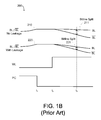
- FIG. 1B is an exemplary graph 200 illustrating the adverse effect that bit line leakage currents can have on the differential voltage between BL and BL during read operations, where line 210 depicts the differential voltage between BL and BL without the effects of leakage current, and line 220 depicts the differential voltage between BL and BL with the effects of leakage current.
- the bit line pre-charge signal PC is asserted to logic high to charge BL and BL high towards V DD .
- PC is de-asserted to turn off pre-charge transistors 121 - 122
- the word line WL is asserted to logic high to turn on access transistors 115 - 116 .
- bit line split 211 on BL and BL without leakage current is much greater than the bit line split 221 on BL and BL with leakage current.
- One approach is to increase the threshold voltage of the transistors in the memory device to reduce the leakage current.
- increasing the transistor threshold voltage undesirably reduces the speed of the memory device, and is not always effective due to the dependence of threshold voltages on process technologies.
- Another approach is to increase the bit line current during read pre-charge operations to offset the leakage current.
- the increase in bit line pre-charge current is typically predetermined using a worst-case leakage current scenario and then applied to all device of the same type (e.g., to a plurality of SRAM devices constructed from the same and/or different wafers).
- a technique to adjust the bit line current in individual columns of a memory array is disclosed in a publication entitled “A Bit line Leakage Compensation Scheme for Low-Voltage SRAMs” by Agawa et al, incorporated herein by reference. That technique measures each bit line's leakage current during the pre-charge cycle of the read operation and then injects a corresponding amount of current to the bit line during the sensing phase of the read operation. Although effective in individually adjusting the current of each bit line, Agawa's technique undesirably limits read speeds because of the time needed to measure the leakage current during the pre-charge phase of each read operation.
- FIG. 1A shows a conventional SRAM cell and leakage current paths therein
- FIG. 1B illustrates the effect of leakage current upon the differential voltage on complementary bit lines during read operations in the SRAM cell of FIG. 1A ;
- FIG. 2A shows a content addressable memory (CAM) device within which present embodiments may be implemented
- FIG. 2B shows a CAM cell employed in the CAM array of FIG. 2A ;
- FIG. 3A shows a column of the CAM array of FIG. 2A in accordance with some embodiments
- FIG. 3B shows a column of the CAM array of FIG. 2A in accordance with other embodiments
- FIG. 4A shows one embodiment of the bit line compensation circuit of FIGS. 3A-3B ;
- FIG. 4B shows another embodiment of the bit line compensation circuit of FIGS. 3A-3B ;
- FIG. 4C shows one embodiment of the leakage detection circuit of FIGS. 3A-3B ;
- FIG. 5 shows an array of memory cells in accordance with other embodiments
- FIG. 6A is an exemplary flow chart illustrating a bit line leakage calibration process in accordance with some embodiments.
- FIG. 6B is an exemplary flow chart illustrating a bit line leakage calibration process in accordance with other embodiments.
- a method and apparatus of compensating for bit line leakage currents in devices containing SRAM cells are described below in the context of a exemplary CAM device for simplicity only. It is to be understood that embodiments of the present invention may be used in any device that employs SRAM cells or latches, including SRAM devices and/or other types of CAM devices.
- specific nomenclature is set forth to provide a thorough understanding of the present invention. However, it will be apparent to one skilled in the art that these specific details may not be required to practice the present invention. In other instances, well-known circuits and devices are shown in block diagram form to avoid obscuring the present invention unnecessarily. Additionally, the interconnection between circuit elements or blocks may be shown as buses or as single signal lines. Each of the buses may alternatively be a single signal line, and each of the single signal lines may alternatively be buses.
- MOS metal oxide semiconductor
- clock signals may alternatively be strobe signals or any other signals that provide timing control.
- dynamic or domino logic circuits described herein, where transistors driven by clock signals are used to pre-charge outputs of the circuits, may be alternatively implemented as static complementary MOS (CMOS) circuits.
- CMOS static complementary MOS
- Present embodiments reduce the effects of undesirable leakage currents in memory devices that contain SRAM cells without sacrificing read speeds.
- Memory devices in accordance with present embodiments are configured to operate in a calibration mode during which the effects of bit line leakage current are measured and to operate in a normal mode during which the bit line current is adjusted to compensate for leakage according to the results of the calibration mode.
- a leakage-free sense operation is performed to determine the differential voltage generated on the bit lines in response to a given stored data value.
- a leakage-susceptible test read operation is performed to determine the differential voltage generated on the bit lines in response to the given stored data value.
- a leakage detection circuit measures the difference between the differential voltages generated in the leakage-free and leakage-susceptible test read operations and generates a compensation signal.
- a bit line compensation circuit selectively adjusts the current provided to the bit lines during the test read operation. This process may be repeated any number of iterations until a value of the compensation signal that results in an amount of bit line compensation current sufficient to compensate for leakage is determined. This final value of the compensation signal is then stored in a suitable compensation memory.
- the leakage detection circuit When the memory device is selected to operate in the normal mode, the leakage detection circuit is disabled, and the compensation signal is read from the compensation memory and provided to the bit line compensation circuit. In response to the bit line compensation signal, the bit line compensation circuit provides the corresponding amount of compensation current to the bit lines for read operations performed during the normal mode.
- the term “normal” mode refers to the operational mode in which read, write, compare, and other operations are performed when the device is employed and operated in an application or system.
- bit line current By selectively determining the amount of bit line current needed to compensate for leakage in an iterative process performed during the calibration mode, present embodiments are advantageous over the various prior art techniques mentioned above. For example, the iterative process by which the bit line current is incrementally increased until the leakage associated with the corresponding device is specifically compensated allows for more precise bit line leakage compensation than indiscriminately injecting a predetermined amount of current into the bit line. Further, determining the amount of bit line compensation current during the calibration mode (e.g., rather than during actual read operations) allows read speeds to be independent of measuring the leakage current, thereby allowing for maximum read speeds.
- each column of the memory device includes its own leakage detection circuit that generates a separate compensation signal for the column's bit line compensation circuit.
- multiple columns of memory cells can share the same leakage detection circuit.
- each block of N columns of the memory device includes its own leakage detection circuit that generates a separate compensation signal for the bit line compensation circuits associated with the block's columns.
- leakage can be addressed on a per-block basis, thereby reducing the overhead of the leakage detection circuitry while still allowing for the leakage in different portions of the memory array to be independently compensated.
- FIG. 2A shows an exemplary CAM device 200 within which present embodiments may be implemented.
- CAM device 200 includes a CAM array 202 that has a plurality of CAM cells (not shown in FIG. 2A for simplicity) arranged in any number of rows and columns.
- the CAM cells in array 202 may be any suitable type of CAM cell including, for example, binary, ternary, and/or quaternary CAM cells.
- One or more instructions and related control signals may be provided to CAM device 200 from an instruction decoder (not shown for simplicity) to control read, write, compare, and/or test operations for CAM device 200 .
- Other well-known signals which may be provided to CAM device 200 , such as enable signals, reset signals, and clock signals, are not shown for simplicity.
- Each row of CAM cells in array 202 is coupled to an address decoder 204 via a corresponding word line WL, and to a priority encoder 206 and to match logic 208 via a corresponding match line ML.
- the word lines and match lines are represented collectively in FIG. 2A for simplicity.
- address decoder 204 receives addresses from an address bus ABUS.
- address decoder 204 receives addresses from another bus.
- the match lines ML provide match results for compare operations to priority encoder 206 , which determines the matching entry that has the highest priority number associated with it and generates the index or address of this highest priority match (HPM).
- Match logic 208 may generate a match flag to indicate a match condition, and may also generate a multiple match flag to indicate multiple matches.
- each row of CAM cells in array 202 may have one or more validity bits to indicate whether the corresponding row (or segment thereof) of CAM cells is in a valid state or an empty state.
- the validity bits may be provided to priority encoder 206 to generate the next free address (NFA) that is available in CAM array 202 for storing new data.
- the validity bits may also be provided to a well-known full flag logic circuit (not shown for simplicity) to generate a full flag and/or empty flag for CAM array 202 .
- Each column of CAM cells in array 202 is coupled to a comparand register 210 via comparand lines CL and to a read/write circuit 212 via bit lines BL.
- Comparand register 210 provides a comparand word (e.g., search key) received from a comparand bus CBUS to CAM array 202 for comparison with entries stored in CAM array 202 .
- comparand words may be provided to comparand register 210 from another bus.
- Read/write circuit 212 includes well-known write drivers and sense amplifiers, and is coupled to a data bus DBUS.
- CAM device 200 may also include a global mask circuit that stores one or more mask patterns that mask entries in CAM array 202 during compare operations with the comparand word provided by comparand register 210 .
- CAM device 200 also includes a leakage detection circuit 214 having a first input to receive a mode select signal MD_SEL, a second input to receive data from the read/write circuit 212 , and an output to provide a bit line compensation signal CPN_BL to CAM array 202 .
- the mode select signal MD_SEL determines whether CAM device 200 operates in the calibration mode or operates in the normal mode.
- MD_SEL can be generated by a user.
- MD_SEL can be generated by a device manufacturer.
- the calibration process can be performed prior to delivery of CAM device 200 to the user, and MD_SEL can be eliminated.
- leakage detection circuit 214 compares the differential voltages generated during leakage-free test read operations and leakage-susceptible test read operations, and in response to the comparison generates CPN_BL. Then, bit line compensation circuitry (not shown in FIG. 2A for simplicity) within or associated with CAM array 202 adjusts the bit line current provided for test read operations.
- detection circuit 214 includes a compensation memory (not shown in FIG. 2A for simplicity) to store the final value of CPN_BL. Thereafter, during normal operation, detection circuit 214 is disabled, and CPN_BL is provided to CAM array 202 to selectively adjust the bit line current for read operations in a manner that compensates for leakage currents while maximizing read speeds.
- CPN_BL can be stored in a suitable memory within or associated with CAM array 202 .
- FIG. 2B shows a binary CAM cell 220 that may be employed in the CAM array of FIG. 2A .
- CAM cell 220 which compares a data bit D with a comparand bit C, includes the SRAM cell 110 of FIG. 1A and a compare circuit 221 .
- Compare circuit 221 includes NMOS transistors 222 , 224 , 226 , and 228 .
- Transistors 222 and 224 are coupled in series between a match line ML and ground potential, with the gate of transistor 222 receiving the data bit D from node 101 and the gate of transistor 224 receiving a complement C of the comparand bit from a complementary comparand line CL .
- Transistors 226 and 228 are coupled in series between match line ML and ground potential, with the gate of transistor 226 receiving the complement D of the data bit from node 102 and the gate of transistor 228 receiving the comparand bit C from the comparand line CL. Read, write, compare, and other operations of CAM array 202 are well-known in the art, and thus are not described herein.
- comparand line pair CL and CL may be eliminated, and bit line pair BL and BL may provide comparand data to CAM cells 220 , as is commonly known in the art.
- FIG. 3A illustrates a column 300 of CAM array 202 in accordance with some embodiments.
- Column 300 includes a plurality of SRAM cells 100 ( 1 )- 100 ( k ), pre-charge circuits 311 A and 311 B, NMOS bit line gating transistors 313 A and 313 B, a sense amplifier 315 , a leakage detection circuit 321 , calibration pre-charge circuits 322 A and 322 B, and bit line compensation circuits 323 A and 323 B.
- SRAM cells 100 ( 1 )- 100 ( k ) are each coupled to bit lines BL and BL .
- FIG. 3A only the SRAM cell portion of the CAM cells are shown, and the comparand lines are omitted.
- column 300 can include corresponding compare circuits 221 and comparand line pairs CL/ CL , as shown in FIG. 2B .
- column 300 can be a column of SRAM cells in an SRAM array.
- the pre-charge circuits 311 A and 311 B are coupled between supply voltage V DD and bit lines BL and BL , respectively, and each have a control terminal to receive a bit line pre-charge signal PC. When PC is asserted, pre-charge circuits 311 A and 311 B pre-charge respective bit lines BL and BL high towards V DD .
- pre-charge circuits 311 A and 311 B are PMOS transistors, although other suitable circuitry can be used for other embodiments.
- Bit line gating transistor 313 A is coupled between the bit line BL and a first input of sense amplifier 315 via a gated bit line GBL, and has a gate to receive a gating transistor enable signal GT_EN.
- Bit line gating transistor 313 B is coupled between the complementary bit line BL and a second input of sense amplifier 315 via a complementary gated bit line GBL , and has a gate to receive GT_EN.
- GT_EN When GT_EN is de-asserted to logic low, gating transistors 313 A and 313 B de-couple BL and BL from sense amplifier 315 .
- GT_EN When GT_EN is asserted to logic high, gating transistors 313 A and 313 B couple BL and BL to sense amplifier 315 .
- Sense amplifier 315 which can be any well-known sensing circuit, has an output to generate a data signal DATA in response to a differential voltage between its inputs.
- Calibration pre-charge circuits 322 A and 322 B are coupled between V DD and GBL and GBL , respectively.
- Calibration pre-charge circuit 322 A has a control terminal to receive a first compensation pre-charge signal CPC_A
- calibration pre-charge circuit 322 B has a control terminal to receive a second compensation pre-charge signal CPC_B.
- Calibration pre-charge circuits 322 A and 322 B selectively pre-charge lines GBL and GBL high towards V DD in response to CPC_A and CPC_B, respectively.
- calibration pre-charge circuits 322 A and 322 B are PMOS transistors, although other suitable circuitry can be used for other embodiments.
- Leakage detection circuit 321 has a first input to receive DATA from sense amplifier 315 , a second input to receive the mode select signal MD_SEL, and an output to generate the bit line compensation signal CPN_BL.
- the bit line compensation circuits 323 A and 323 B are coupled between V DD and BL and BL , respectively, and have control terminals to receive first and second bit line compensation signals CPN_BLA and CPN_BLB, respectively.
- Bit line compensation circuits 323 A and 323 B selectively adjust the amount of bit line current provided during read operations in response to CPN_BLA and CPN_BLB, respectively, as described in detail below.
- present embodiments are configured to operate in a calibration mode during which the effects of bit line leakage current are measured and to operate in a normal mode during which the bit line current is adjusted to compensate for leakage according to the leakage results determined during the calibration mode.
- column 300 enters the calibration mode when MD_SEL is asserted to a first state, which enables leakage detection circuit 321 .
- the first state of MD_SEL can be used to disable comparand register 210 , priority encoder 206 , and/or match logic 208 (see also FIG. 2A ).
- the signal GT_EN is de-asserted to logic low, which turns off gating transistors 313 A and 313 B to de-couple the bit lines BL and BL from sense amplifier 315 .
- the signal CPC_A is asserted to logic high to turn on the calibration pre-charge circuit 322 A, which pre-charges the gated bit line GBL high towards V DD , and the signal CPC_B is de-asserted to logic low to turn off the calibration pre-charge circuit 322 B, thereby maintaining GBL in a logic low state.
- This data value is hereinafter referred to as the reference data value DATA_REF because it corresponds to the leakage-free sense operation, to which the results of subsequent test read operations are referenced (e.g., compared).
- the value DATA_REF is stored in a suitable memory element (not shown for simplicity) provided within or associated with leakage detection circuit 321 .
- DATA_REF is a digital value.
- DATA_REF is an analog value. Because the gated bit lines GBL and GBL are not coupled to any of the SRAM cells 100 , this sense operation is designated as leakage free.
- the signal GT_EN is asserted to logic high, which turns on gating transistors 313 A and 313 B to couple the bit lines BL and BL to sense amplifier 315 .
- Signals CPC_A and CPC_B are de-asserted to logic low to turn off the calibration pre-charge circuits 322 A and 322 B, thereby isolating GBL and GBL from V DD .
- Pre-charge signal PC is asserted to turn on pre-charge circuits 311 A and 311 B, which in turn pre-charge BL and BL high towards V DD .
- This data value is hereinafter referred to as the first leakage data value DATA_LK 1 because it corresponds to the first leakage-susceptible test read operation.
- the value of DATA_LK 1 is stored in a suitable memory element (not shown for simplicity) provided within or associated with leakage detection circuit 321 . Because there is leakage current 103 in the selected SRAM cell 100 of column 300 , this first test read operation is designated as leakage-susceptible.
- the values DATA_REF and DATA_LK 1 generated by sense amplifier 315 are compared to generate a first value of CPN_BLA and CPN_BLB that indicates whether the differential voltage between BL and BL generated during the first leakage-susceptible test read operation is detectable by sense amplifier 315 . For example, if the differential voltage between BL and BL is sufficient to be detected by sense amplifier 315 , then the value of DATA_LK 1 matches the value of DATA_REF, and CPN_BL indicates that bit line current compensation is not desired.
- bit line compensation circuit 321 includes well-known digital comparators to compare the first and second values of DATA.
- bit line compensation circuit 321 includes well-known analog compare circuitry to compare the first and second values of DATA.
- bit line compensation circuit 321 is a microprocessor programmed to perform the above-described functions.
- leakage detection circuit 321 provides the current value of CPN_BLA and CPN_BLB to bit line compensation circuits 323 A and 323 B, which in response thereto selectively adjust the bit line current for the next test read operation.
- GT_EN remains asserted so that gating transistors 313 A and 313 B couple the bit lines BL and BL to sense amplifier 315 , and signals CPC_A and CPC_B remain de-asserted so that calibration pre-charge circuits 322 A and 322 B isolate GBL and GBL from V DD .
- Pre-charge signal PC is asserted to turn on pre-charge circuits 311 A and 311 B, which in turn pre-charge BL and BL high towards V DD .
- the asserted states of CPN_BLA and CPN_BLB turn on bit line compensation circuits 323 A and 323 B to increase the bit line current for the second test read operation.
- This data value is hereinafter referred to as the second leakage data value DATA_LK 2 because it corresponds to the second leakage-susceptible test read operation.
- the value of DATA_LK 2 is stored in a suitable memory element (not shown for simplicity) provided within or associated with leakage detection circuit 321 . Because there is leakage current 103 in the selected SRAM cell 100 of column 300 , this second test read operation is designated as leakage-susceptible.
- the values DATA_REF and DATA_LK 2 generated by sense amplifier 315 are compared to determine whether the differential voltage between BL and BL generated during the second leakage-susceptible test read operation is detectable by sense amplifier 315 . If DATA_LK 2 does not match DATA_REF, thereby indicating that the additional amount of bit line current provided by bit line compensation circuits 323 A and 323 B during the second test read operation was not sufficient to generate a differential voltage between BL and BL that can be detected by sense amplifier 315 , another leakage-susceptible test read operation may be selectively performed in the manner described above.
- MD_SEL is driven to a second state.
- the second state of MD_SEL disables leakage detection circuit 321 .
- the second state of MD_SEL also maintains the CPC signals in de-asserted states so that calibration pre-charge circuits 322 A and 322 B isolate GBL and GBL , respectively, from V DD , and maintains GT_EN in its de-asserted state so that gating transistors couple BL and BL to the sense amplifier 315 .
- the second state of MD_SEL can be used to enable comparand register 210 , priority encoder 206 , and/or match logic 208 for compare operations in CAM device 200 during the normal operational mode.
- bit line compensation circuits 323 A and 323 B For read operations performed in the normal mode, the final values of CPN_BLA and CPN_BLB determined during the calibration mode are provided to bit line compensation circuits 323 A and 323 B, which in response thereto provide the corresponding amount of compensation current to BL and BL , respectively.
- the bit line compensation current provided by bit line compensation circuits 323 A and 323 B accurately compensates for leakage in SRAM cells 100 , thereby improving the reliability of data read from column 300 .
- the amount of bit line compensation current is selected during the calibration mode, the read speeds are not adversely affected by the time associated with measuring the leakage effects.
- the bit line compensation current provided by the bit line compensation circuits 323 is an adjustable current that is selectively determined by the leakage detection circuit 321 during the calibration mode.
- the bit line compensation current is determined based on an iterative process of comparisons between the leakage-free sensed data and one or more leakage-susceptible test read data.
- the bit line control circuit 321 may be configured to increase the bit line compensation current incrementally during the iterative process until the leakage-susceptible read data matches the leakage-free reference data or until a maximum bit line current is reached.
- any suitable data can be programmed into the non-selected SRAM cells 100 to achieve varying levels and/or models of leakage in column 300 .
- FIG. 3B illustrates a column 301 of CAM array 202 in accordance with other embodiments.
- Column 301 is similar to column 300 of FIG. 3A , except that column 301 includes two sense amplifiers 341 and 342 instead of one sense amplifier 315 .
- First sense amplifier 341 has inputs coupled to GBL and GBL , and has an output to provide the sensed data DATA for read operations performed during the normal operational mode.
- Second sense amplifier 342 has inputs coupled to GBL and GBL , and has an output to provide calibration data DATA_CAL for test read operations performed during the calibration mode.
- Sense amplifiers 341 and 342 can be any well-known sensing circuits that detect a differential voltage between GBL and GBL and generate a data signal indicative thereof.
- first sense amplifier 341 is active only during the normal operational mode and is optimized to achieve maximum reads speeds
- second sense amplifier 342 is active only during the calibration mode and is optimized for maximum sensitivity.
- second sense amplifier 342 is configured to resolve smaller differential voltages between BL and BL than first sense amplifier 341
- first sense amplifier 341 is configured to perform quick sense amplifications during the normal operational mode.
- second sense amplifier 342 can be used to perform more accurate although typically slower data sensing operations (e.g., compared to first sense amplifier 341 ) during the calibration mode, and first sense amplifier 341 can be used to perform faster data sense operations (e.g., compared to second sense amplifier 341 ) during the normal operational mode.
- FIG. 4A illustrates a bit line compensation circuit 410 that is one embodiment of the bit line compensation circuits 323 A and 323 B of FIGS. 3A and 3B .
- bit line compensation circuit 410 is a PMOS transistor coupled between V DD and one of the bit lines (BL or BL ) and having a gate to receive the bit line compensation signal CPN_BL.
- Transistor 410 selectively provides an additional amount of bit line current (e.g., in addition to pre-charge circuits 311 ) to compensate for leakage in response to CPN_BL.
- CPN_BL is a digital signal (e.g., either logic high or logic low) that either turns on or turns off transistor 410 .
- CPN_BL is an analog signal whose voltage can be incrementally increased during successive test read operations to iteratively decrease the bit line current provided by transistor 410 .
- FIG. 4B shows a bit line compensation circuit 420 that is another embodiment of the bit line compensation circuits 323 A and 323 B of FIGS. 3A and 3B .
- the bit line compensation circuit 420 includes a plurality of PMOS transistors 421 ( 1 )- 421 ( n ) connected in parallel between V DD and one of the bit lines (BL or BL ).
- Each of the PMOS transistors 421 ( 1 )- 421 ( n ) has a gate to receive a corresponding bit of the bit line compensation signal CPN_BL (as indicated in FIG. 4B ), which controls the conductivity of the corresponding PMOS pull-up transistor 421 .
- the bit line current provided by circuit 420 can be selectively adjusted by dynamically selecting how many of the PMOS pull-up transistors 421 ( 1 )- 421 ( n ) are conductive. For example, asserting none of CPN_BL[n:1] turns on none of the PMOS pull-up transistors 421 ( 1 )- 421 ( n ), thereby providing no bit line compensation current.
- Asserting one of CPN_BL[n:1] turns on one of the PMOS pull-up transistors 421 ( 1 )- 421 ( n ) to provide a bit line compensation current
- asserting two of CPN_BL[n:1] turns on two of the PMOS pull-up transistors 421 ( 1 )- 421 ( n ) to provide an increased bit line compensation current
- asserting all of CPN_BL[n:1] turns on all of the PMOS pull-up transistors 421 ( 1 )- 421 ( n ) to provide a maximum bit line compensation current.
- PMOS transistors 421 ( 1 )- 421 ( n ) are constructed to be of similar size and to have similar operating characteristics so that when conductive, each of transistors 421 ( 1 )- 421 ( n ) provides the same amount of compensation current to the associated bit line.
- PMOS pull-up transistors 421 ( 1 )- 421 ( n ) can be constructed to conduct varying amounts of current when turned on.
- transistors 421 ( 1 )- 421 ( n ) can be sized according to a binary scheme, where for example, transistor 421 ( x ) provides twice the current as transistor 421 ( x ⁇ 1), where x is an integer between 2 and n.
- FIG. 4C shows a leakage detection circuit 430 that is one embodiment of leakage detection circuit 321 of FIGS. 3A and 3B .
- Leakage detection circuit 430 which includes a data memory 411 , a compare circuit 412 , count logic 413 , and a control circuit 414 , is configured to generate an n-bit signal CPN_BL that can be used to control the bit line compensation circuit 420 of FIG. 4B .
- Data memory 411 which can be any suitable memory element or device, has an input to receive the data signal from the output of sense amplifier 315 (see also FIG. 3A ), and has outputs to provide DATA_REF and DATA_LK to compare circuit 412 .
- Count logic 413 which has a first input to receive INC from compare circuit 412 and a second input to receive an enable signal CNT_EN from control circuit 414 , selectively increments a count value in response to INC to generate the n-bit output signal CPN_BL. For exemplary embodiments described herein, count logic 413 increments the count value by one if INC is asserted, and maintains the current value of the count value if INC is de-asserted. For some embodiments, count logic 413 outputs the count value as a decoded value to generate CPN_BL. As described above, CPN_BL can be used to control the amount of compensation current provided to the bit lines of memory columns in array 202 by the bit line compensation circuits 323 A and 323 B. Control circuit 414 controls read and write operations of data memory 411 using a data select signal DATA_SEL, and controls the count logic 413 with the enable signal CNT_EN.
- leakage detection circuit 420 An exemplary operation of leakage detection circuit 420 is described below with reference to column 300 of FIG. 3A .
- the values DATA_REF and DATA_LK 1 generated by sense amplifier 315 are stored in data memory 411 .
- DATA_REF and DATA_LK 1 are stored in data memory 411 during a write operations controlled by control circuit 414 using DATA_SEL, which may include, for example, write enable signals and write addresses.
- each column of memory cells includes its own leakage detection circuit, which allows leakage to be addressed on a per-column basis.
- multiple columns of memory cells can share the same leakage detection circuit.
- FIG. 5 shows a memory block 500 in accordance with other embodiments.
- Memory block 500 is shown to include a plurality of columns 501 ( 1 )- 501 ( m ), each including a number of memory cells 100 , a corresponding bit line compensation circuit 323 , and a corresponding sense amplifier 315 .
- the sense amplifier 315 in each of columns 501 ( 1 )- 501 ( m ) generates a corresponding bit of the data word DATA[m:1].
- the data bit DATA[1] generated by the sense amplifier 315 in the first column 500 ( 1 ) of memory cells 100 is provided to leakage detection circuit 321 , which is shared by all columns 500 ( 1 )- 500 ( m ).
- the same bit line compensation signal CPN_BL generated by leakage detection circuit 321 is provided to the bit line compensation circuits 323 in all of the columns 500 ( 1 )- 500 ( m ). In this manner, leakage can be addressed on a per-block basis, thereby reducing the overhead of the leakage detection circuitry by allowing multiple columns 500 ( 1 )- 500 ( m ) to share the same leakage detection circuit 321 .
- the data signals output from the sense amplifiers 315 in all columns 501 ( 1 )- 501 ( m ) can be multiplexed to select one of the signals to be provided to leakage detection circuit 321 , and the output CPN_BL of detection circuit 321 can be selectively applied to the corresponding compensation circuits 323 .
- FIG. 6A is an exemplary flow chart illustrating operation of column 300 during the calibration mode for some embodiments, with reference to FIGS. 2A , 2 B, and 3 A.
- column 300 enters the calibration mode ( 601 ).
- the calibration mode may be entered by driving the mode select signal MD_SEL to the first state.
- MD_SEL can be controlled by a user.
- MD_SEL can be triggered periodically by a timer (not shown for simplicity) provided within the memory device.
- the memory device may be configured to enter the calibration mode when it is detected that the ambient temperature has changed by a pre-determined amount to automatically compensate for changes in leakage caused by temperature variations.
- the bit lines are de-coupled from the sense amplifier 315 ( 602 ).
- the bit lines are de-coupled from the sense amplifier by turning off the bit line gating transistors 313 A and 313 B.
- one of the inputs of the sense amplifier is charged high toward V DD by the corresponding calibration pre-charge circuit 322 to develop a differential voltage between the sense amplifier inputs (e.g., to model a data bit stored in one SRAM cell 100 ) ( 603 ).
- the leakage-free sense operation is performed to generate the reference data signal DATA_REF ( 604 ), and DATA_REF is stored in a suitable memory (e.g., within or associated with leakage detection circuit 321 ) ( 605 ).
- bit lines (BL and BL ) are coupled to the sense amplifier 315 , for example, by turning on the bit line gating transistors 313 A and 313 B ( 606 ).
- the bit lines are then pre-charged high towards V DD ( 607 ), and then the leakage-susceptible test read is performed to generate DATA_LK ( 608 ). Because the leakage-susceptible test read operation is performed with the bit lines coupled to the sense amplifier, bit line leakage currents affect the differential voltage developed between the complementary bit lines BL and BL .
- bit line current compensation is enabled ( 612 ). For example, referring also to FIG. 4A , if bit line current adjustment is desired, CPN_BL is asserted to turn on bit line compensation transistor 410 , which increases the bit line current provided during read operations.
- FIG. 6B is an exemplary flow chart illustrating operation of column 300 during the calibration mode for other embodiments, with reference to FIGS. 2A , 2 B, and 3 A.
- the exemplary embodiment of FIG. 6B is similar to that of FIG. 6A , except that the embodiment of FIG. 6B includes an iterative process by which the bit line current can be incrementally increased in response to successive leakage-susceptible test read operations.
- Steps 601 - 611 of the flow chart of FIG. 6B are similar to those of FIG. 6A , and thus will not be repeated. If DATA_LK does not match DATA_REF at 610 , it is determined if the maximum bit line current has been reached ( 620 ). If so, the calibration mode ends at 611 . If not, the bit line current is incrementally increased ( 621 ). For example, referring also to FIG. 4B , if bit line current adjustment is desired, one of the bits of CPN_BL is asserted to turn on a corresponding one of the PMOS pull-up transistors 421 , thereby increasing the bit line current provided for read operations. Then, processing continues at 607 . In this manner, the bit line compensation current can be incrementally increased in successive test read operations until the total bit line current provided for read operations results in data being corrected sensed by the sense amplifier.
- the first leakage-susceptible test read operation is performed with none of the PMOS pull-up transistors 421 conductive, thereby starting the calibration mode with no bit line current compensation.
- one or more of PMOS pull-up transistors 421 can be enabled at the beginning of the calibration mode, for example, by storing a predetermined value of CPN_BL.
- determining whether the maximum bit line compensation current is reached at 620 can be performed by detecting a maximum decoded value of CPN_BL (e.g., when CPN_BL has turned on all PMOS pull-up transistors 421 ( 1 )- 421 ( n )).
Abstract
Description
Claims (24)
Priority Applications (1)
| Application Number | Priority Date | Filing Date | Title |
|---|---|---|---|
| US12/771,657 US7920397B1 (en) | 2010-04-30 | 2010-04-30 | Memory device having bit line leakage compensation |
Applications Claiming Priority (1)
| Application Number | Priority Date | Filing Date | Title |
|---|---|---|---|
| US12/771,657 US7920397B1 (en) | 2010-04-30 | 2010-04-30 | Memory device having bit line leakage compensation |
Publications (1)
| Publication Number | Publication Date |
|---|---|
| US7920397B1 true US7920397B1 (en) | 2011-04-05 |
Family
ID=43805877
Family Applications (1)
| Application Number | Title | Priority Date | Filing Date |
|---|---|---|---|
| US12/771,657 Expired - Fee Related US7920397B1 (en) | 2010-04-30 | 2010-04-30 | Memory device having bit line leakage compensation |
Country Status (1)
| Country | Link |
|---|---|
| US (1) | US7920397B1 (en) |
Cited By (10)
| Publication number | Priority date | Publication date | Assignee | Title |
|---|---|---|---|---|
| US8780650B2 (en) * | 2012-03-27 | 2014-07-15 | Apple Inc. | Memory with redundant sense amplifier |
| CN103988432A (en) * | 2011-12-15 | 2014-08-13 | 国际商业机器公司 | Digital voltage boost circuit |
| US9191022B2 (en) | 2012-10-16 | 2015-11-17 | Lattice Semiconductor Corporation | Leakage-current abatement circuitry for memory arrays |
| US10157672B2 (en) * | 2017-04-25 | 2018-12-18 | International Business Machines Corporation | SRAM bitline equalization using phase change material |
| US20190088317A1 (en) * | 2017-09-18 | 2019-03-21 | Nxp Usa, Inc. | Resistive non-volatile memory and a method for sensing a memory cell in a resistive non-volatile memory |
| CN112259147A (en) * | 2020-10-21 | 2021-01-22 | 海光信息技术股份有限公司 | Content addressable memory, array and processor system |
| CN113257295A (en) * | 2020-02-10 | 2021-08-13 | 台湾积体电路制造股份有限公司 | Memory circuit and method of controlling multi-stage precharge circuit |
| CN115050406A (en) * | 2022-08-17 | 2022-09-13 | 安徽大学 | Bit line leakage current compensation circuit and module of SRAM (static random Access memory) and memory |
| US11948624B2 (en) * | 2021-12-23 | 2024-04-02 | Microsoft Technology Licensing, Llc | Memory bit cell array including contention-free column reset circuit, and related methods |
| CN113257295B (en) * | 2020-02-10 | 2024-04-12 | 台湾积体电路制造股份有限公司 | Memory circuit and method for controlling multi-stage precharge circuit |
Citations (88)
| Publication number | Priority date | Publication date | Assignee | Title |
|---|---|---|---|---|
| US4045781A (en) | 1976-02-13 | 1977-08-30 | Digital Equipment Corporation | Memory module with selectable byte addressing for digital data processing system |
| US4523301A (en) | 1982-06-04 | 1985-06-11 | Matsushita Electric Industrial Co., Ltd. | Associative memory |
| US5045899A (en) | 1989-12-01 | 1991-09-03 | Mitsubishi Denki Kabushiki Kaisha | Dynamic random access memory having stacked capacitor structure |
| US5062077A (en) | 1989-07-31 | 1991-10-29 | Kabushiki Kaisha Toshiba | Dynamic type semiconductor memory device |
| US5136543A (en) | 1989-05-12 | 1992-08-04 | Mitsubishi Denki Kabushiki Kaisha | Data descrambling in semiconductor memory device |
| US5140556A (en) | 1988-08-01 | 1992-08-18 | Oki Electric Industry Co., Ltd. | Semiconductor memory circuit having dummy cells connected to twisted bit lines |
| US5276649A (en) | 1989-03-16 | 1994-01-04 | Mitsubishi Denki Kabushiki Kaisha | Dynamic-type semiconductor memory device having staggered activation of column groups |
| US5280443A (en) | 1986-12-11 | 1994-01-18 | Mitsubishi Denki Kabushiki Kaisha | Bit line structure for semiconductor memory device |
| US5327372A (en) | 1992-01-17 | 1994-07-05 | Matsushita Electric Industrial Co., Ltd. | Semiconductor memory device |
| US5383159A (en) | 1992-09-17 | 1995-01-17 | Sharp Kabushiki Kaisha | Semiconductor memory device of alternately-activated open bit-line architecture |
| US5396449A (en) | 1993-12-21 | 1995-03-07 | International Business Machines Corporation | Fast content addressable memory with reduced power consumption |
| US5440715A (en) | 1990-06-27 | 1995-08-08 | Advanced Micro Devices, Inc. | Method and apparatus for expanding the width of a content addressable memory using a continuation bit |
| US5446685A (en) | 1993-02-23 | 1995-08-29 | Intergraph Corporation | Pulsed ground circuit for CAM and PAL memories |
| US5483480A (en) | 1993-07-22 | 1996-01-09 | Kawasaki Steel Corporation | Method of using associative memories and an associative memory |
| US5488583A (en) | 1994-09-22 | 1996-01-30 | Micron Technology, Inc. | Memory integrated circuits having on-chip topology logic driver, and methods for testing and producing such memory integrated circuits |
| US5499218A (en) | 1995-01-31 | 1996-03-12 | Goldstar Electron Co., Ltd. | Method for driving bit line selecting signals |
| US5517441A (en) | 1994-12-14 | 1996-05-14 | International Business Machines Corporation | Content addressable memory circuitry and method of operation |
| US5534732A (en) | 1994-08-15 | 1996-07-09 | International Business Machines Corporation | Single twist layout and method for paired line conductors of integrated circuits |
| US5649126A (en) | 1995-12-04 | 1997-07-15 | Sun Microsystems, Inc. | Parallel signal bus with reduced miller effect capacitance |
| US5699288A (en) | 1996-07-18 | 1997-12-16 | International Business Machines Corporation | Compare circuit for content-addressable memories |
| US5706224A (en) | 1996-10-10 | 1998-01-06 | Quality Semiconductor, Inc. | Content addressable memory and random access memory partition circuit |
| US5740097A (en) | 1994-11-28 | 1998-04-14 | International Business Machines Corporation | Content-addressable-memory control circuit |
| US5818786A (en) | 1995-05-24 | 1998-10-06 | Kawasaki Steel Corporation | Layout method of semiconductor memory and content-addressable memory |
| US5852569A (en) | 1997-05-20 | 1998-12-22 | Quality Semiconductor, Inc. | Content addressable memory multiple match detection circuit |
| US5859791A (en) | 1997-01-09 | 1999-01-12 | Northern Telecom Limited | Content addressable memory |
| US5936873A (en) | 1997-09-30 | 1999-08-10 | Sun Microsystems, Inc. | Single ended match sense amplifier |
| US5964857A (en) | 1997-05-30 | 1999-10-12 | Quality Semiconductor, Inc. | Priority encoder for a content addressable memory system |
| US5966319A (en) | 1997-07-15 | 1999-10-12 | Mitsubishi Denki Kabushiki Kaisha | Static memory device allowing correct data reading |
| US5978246A (en) | 1997-09-08 | 1999-11-02 | Nec Corporation | Content addressable memory device |
| US6044005A (en) | 1999-02-03 | 2000-03-28 | Sibercore Technologies Incorporated | Content addressable memory storage device |
| US6075729A (en) | 1997-09-05 | 2000-06-13 | Hitachi, Ltd. | High-speed static random access memory |
| US6101116A (en) | 1999-06-30 | 2000-08-08 | Integrated Device Technology, Inc. | Six transistor content addressable memory cell |
| US6101115A (en) | 1998-08-07 | 2000-08-08 | Cisco Technology, Inc. | CAM match line precharge |
| US6125049A (en) | 1999-01-05 | 2000-09-26 | Netlogic Microsystems, Inc. | Match line control circuit for content addressable memory |
| US6128207A (en) | 1998-11-02 | 2000-10-03 | Integrated Device Technology, Inc. | Low-power content addressable memory cell |
| US6166939A (en) | 1999-07-12 | 2000-12-26 | Net Logic Microsystems | Method and apparatus for selective match line pre-charging in a content addressable memory |
| US6175514B1 (en) | 1999-01-15 | 2001-01-16 | Fast-Chip, Inc. | Content addressable memory device |
| US6191969B1 (en) | 1999-09-09 | 2001-02-20 | Net Logic Microsystems, Inc. | Selective match line discharging in a partitioned content addressable memory array |
| US6195278B1 (en) | 1999-12-30 | 2001-02-27 | Nortel Networks Limited | Content addressable memory cells and words |
| US6243280B1 (en) | 1999-09-09 | 2001-06-05 | Netlogic Microsystems, Inc. | Selective match line pre-charging in a partitioned content addressable memory array |
| US6243281B1 (en) | 2000-06-14 | 2001-06-05 | Netlogic Microsystems, Inc. | Method and apparatus for accessing a segment of CAM cells in an intra-row configurable CAM system |
| US6246601B1 (en) | 2000-06-14 | 2001-06-12 | Netlogic Microsystems, Inc. | Method and apparatus for using an inter-row configurable content addressable memory |
| US6252789B1 (en) | 2000-06-14 | 2001-06-26 | Netlogic Microsystems, Inc. | Inter-row configurability of content addressable memory |
| US6256241B1 (en) | 2000-03-30 | 2001-07-03 | Intel Corporation | Short write test mode for testing static memory cells |
| US6256216B1 (en) | 2000-05-18 | 2001-07-03 | Integrated Device Technology, Inc. | Cam array with minimum cell size |
| US6262929B1 (en) | 1999-02-05 | 2001-07-17 | International Business Machines Corporation | Pre-charging circuit and method for a word match line of a content add ressable memory (CAM) |
| US6262907B1 (en) | 2000-05-18 | 2001-07-17 | Integrated Device Technology, Inc. | Ternary CAM array |
| US6282113B1 (en) | 1999-09-29 | 2001-08-28 | International Business Machines Corporation | Four F-squared gapless dual layer bitline DRAM array architecture |
| US6292383B1 (en) | 2000-04-27 | 2001-09-18 | Stmicroelectronics, Inc. | Redundant memory cell for dynamic random access memories having twisted bit line architectures |
| US6324087B1 (en) | 2000-06-08 | 2001-11-27 | Netlogic Microsystems, Inc. | Method and apparatus for partitioning a content addressable memory device |
| US6331942B1 (en) | 2000-09-09 | 2001-12-18 | Tality, L.P. | Content addressable memory cell and design methodology utilizing grounding circuitry |
| US6341079B1 (en) | 2001-05-23 | 2002-01-22 | International Business Machines Corporation | Content addressable memory device |
| US6343029B1 (en) | 2001-02-13 | 2002-01-29 | Silicon Access Networks, Inc. | Charge shared match line differential generation for CAM |
| US6349049B1 (en) | 2001-03-22 | 2002-02-19 | Sun Microsystems, Inc. | High speed low power content addressable memory |
| US6370613B1 (en) | 1999-07-27 | 2002-04-09 | Integrated Device Technology, Inc. | Content addressable memory with longest match detect |
| US6373738B1 (en) | 2000-11-20 | 2002-04-16 | International Business Machines Corporation | Low power CAM match line circuit |
| US6430074B1 (en) | 1999-09-09 | 2002-08-06 | Netlogic Mircosystems, Inc. | Selective look-ahead match line pre-charging in a partitioned content addressable memory array |
| US6442061B1 (en) | 2001-02-14 | 2002-08-27 | Lsi Logic Corporation | Single channel four transistor SRAM |
| US6452822B1 (en) | 2001-04-26 | 2002-09-17 | International Business Machines Corporation | Segmented match line arrangement for content addressable memory |
| US6483733B2 (en) | 1999-03-31 | 2002-11-19 | Mosaid Technologies Incorporated | Dynamic content addressable memory cell |
| US6499081B1 (en) | 1999-02-23 | 2002-12-24 | Netlogic Microsystems, Inc. | Method and apparatus for determining a longest prefix match in a segmented content addressable memory device |
| US6500706B1 (en) | 2001-03-19 | 2002-12-31 | Taiwan Semiconductor Manufacturing Company | Bit-line interconnection scheme for eliminating coupling noise in stack DRAM cell with capacitor under bit-line (CUB) in stand-alone or embedded DRAM |
| US20030002351A1 (en) | 2001-06-23 | 2003-01-02 | Peter Beer | Integrated memory circuit and method for reading a data item from a memory cell |
| US6512682B2 (en) | 2001-03-29 | 2003-01-28 | Intel Corporation | Power supply with interface to determine power requirements of devices coupled thereto |
| US20030070039A1 (en) | 2001-09-28 | 2003-04-10 | Peter Gillingham | Circuit and method for performing variable width searches in a content addressable memory |
| US6560670B1 (en) | 2000-06-14 | 2003-05-06 | Netlogic Microsystems, Inc. | Inter-row configurability of content addressable memory |
| US6563727B1 (en) | 2002-07-31 | 2003-05-13 | Alan Roth | Method and structure for reducing noise effects in content addressable memories |
| US6570794B1 (en) | 2001-12-27 | 2003-05-27 | Infineon Technologies North America Corp. | Twisted bit-line compensation for DRAM having redundancy |
| US20030123269A1 (en) | 2001-12-31 | 2003-07-03 | Peter Gillingham | Circuit and method for reducing power usage in a content addressable memory |
| US6597596B2 (en) | 2001-06-11 | 2003-07-22 | International Business Machines Corporation | Content addressable memory having cascaded sub-entry architecture |
| US6597594B2 (en) | 2000-03-17 | 2003-07-22 | Silicon Aquarius, Inc. | Content addressable memory cells and systems and devices using the same |
| US6646900B2 (en) | 2001-10-31 | 2003-11-11 | Kawasaki Microelectronics, Inc. | Ternary content addressable memory with data and mask data settable therewithin by one write cycle |
| US6657880B1 (en) | 2002-12-04 | 2003-12-02 | Virtual Silicon Technology, Inc. | SRAM bit line architecture |
| US6697277B2 (en) | 2001-08-06 | 2004-02-24 | International Business Machines Corporation | Content addressable memory (CAM) having a match line circuit with selectively adjustable pull-up impedances |
| US6760241B1 (en) * | 2002-10-18 | 2004-07-06 | Netlogic Microsystems, Inc. | Dynamic random access memory (DRAM) based content addressable memory (CAM) cell |
| US6785179B1 (en) | 2003-06-19 | 2004-08-31 | Arm Limited | Charge sharing between bit lines within a memory circuit to increase recharge speed |
| US6795325B1 (en) | 2003-03-26 | 2004-09-21 | Renesas Technology Corp. | Semiconductor memory |
| US6804134B1 (en) | 2002-04-10 | 2004-10-12 | Integrated Device Technology, Inc. | Content addressable memory (CAM) devices having CAM array blocks therein that conserve bit line power during staged compare operations |
| US6803610B2 (en) | 2002-09-30 | 2004-10-12 | Mosaid Technologies Incorporated | Optimized memory cell physical arrangement |
| US6807077B2 (en) | 2002-12-13 | 2004-10-19 | Renesas Technology Corp. | Content addressable memory capable of stably storing ternary data |
| US6879504B1 (en) | 2001-02-08 | 2005-04-12 | Integrated Device Technology, Inc. | Content addressable memory (CAM) devices having error detection and correction control circuits therein and methods of operating same |
| US6888730B2 (en) | 2001-04-03 | 2005-05-03 | Mosaid Technologies Incorporated | Content addressable memory cell |
| US6900999B1 (en) | 2003-06-30 | 2005-05-31 | Integrated Device Technology, Inc. | Ternary content addressable memory (TCAM) cells with small footprint size and efficient layout aspect ratio |
| US6901000B1 (en) | 2003-05-30 | 2005-05-31 | Netlogic Microsystems Inc | Content addressable memory with multi-ported compare and word length selection |
| US6906937B1 (en) | 2003-03-21 | 2005-06-14 | Netlogic Microsystems, Inc. | Bit line control circuit for a content addressable memory |
| US7319602B1 (en) | 2004-07-01 | 2008-01-15 | Netlogic Microsystems, Inc | Content addressable memory with twisted data lines |
| US7355890B1 (en) | 2006-10-26 | 2008-04-08 | Integrated Device Technology, Inc. | Content addressable memory (CAM) devices having NAND-type compare circuits |
| US20100271854A1 (en) | 2009-04-28 | 2010-10-28 | Integrated Device Technology, Inc. | Ternary Content Addressable Memory Having Reduced Leakage Effects |
-
2010
- 2010-04-30 US US12/771,657 patent/US7920397B1/en not_active Expired - Fee Related
Patent Citations (99)
| Publication number | Priority date | Publication date | Assignee | Title |
|---|---|---|---|---|
| US4045781A (en) | 1976-02-13 | 1977-08-30 | Digital Equipment Corporation | Memory module with selectable byte addressing for digital data processing system |
| US4523301A (en) | 1982-06-04 | 1985-06-11 | Matsushita Electric Industrial Co., Ltd. | Associative memory |
| US5461589A (en) | 1986-12-11 | 1995-10-24 | Mitsubishi Denki Kabushiki Kaisha | Bit line structure for semiconductor memory device with bank separation at cross-over regions |
| US5280443A (en) | 1986-12-11 | 1994-01-18 | Mitsubishi Denki Kabushiki Kaisha | Bit line structure for semiconductor memory device |
| US5416734A (en) | 1986-12-11 | 1995-05-16 | Mitsubishi Denki Kabushiki Kaisha | Bit line structure for semiconductor memory device |
| US5550769A (en) | 1986-12-11 | 1996-08-27 | Mitsubishi Denki Kabushiki Kaisha | Bit line structure for semiconductor memory device |
| US5140556A (en) | 1988-08-01 | 1992-08-18 | Oki Electric Industry Co., Ltd. | Semiconductor memory circuit having dummy cells connected to twisted bit lines |
| US5276649A (en) | 1989-03-16 | 1994-01-04 | Mitsubishi Denki Kabushiki Kaisha | Dynamic-type semiconductor memory device having staggered activation of column groups |
| US5136543A (en) | 1989-05-12 | 1992-08-04 | Mitsubishi Denki Kabushiki Kaisha | Data descrambling in semiconductor memory device |
| US5062077A (en) | 1989-07-31 | 1991-10-29 | Kabushiki Kaisha Toshiba | Dynamic type semiconductor memory device |
| US5045899A (en) | 1989-12-01 | 1991-09-03 | Mitsubishi Denki Kabushiki Kaisha | Dynamic random access memory having stacked capacitor structure |
| US5440715A (en) | 1990-06-27 | 1995-08-08 | Advanced Micro Devices, Inc. | Method and apparatus for expanding the width of a content addressable memory using a continuation bit |
| US5327372A (en) | 1992-01-17 | 1994-07-05 | Matsushita Electric Industrial Co., Ltd. | Semiconductor memory device |
| US5383159A (en) | 1992-09-17 | 1995-01-17 | Sharp Kabushiki Kaisha | Semiconductor memory device of alternately-activated open bit-line architecture |
| US5598115A (en) | 1993-02-23 | 1997-01-28 | Intergraph Corporation | Comparator cell for use in a content addressable memory |
| US5446685A (en) | 1993-02-23 | 1995-08-29 | Intergraph Corporation | Pulsed ground circuit for CAM and PAL memories |
| US5483480A (en) | 1993-07-22 | 1996-01-09 | Kawasaki Steel Corporation | Method of using associative memories and an associative memory |
| US5396449A (en) | 1993-12-21 | 1995-03-07 | International Business Machines Corporation | Fast content addressable memory with reduced power consumption |
| US5534732A (en) | 1994-08-15 | 1996-07-09 | International Business Machines Corporation | Single twist layout and method for paired line conductors of integrated circuits |
| US5488583A (en) | 1994-09-22 | 1996-01-30 | Micron Technology, Inc. | Memory integrated circuits having on-chip topology logic driver, and methods for testing and producing such memory integrated circuits |
| US5740097A (en) | 1994-11-28 | 1998-04-14 | International Business Machines Corporation | Content-addressable-memory control circuit |
| US5517441A (en) | 1994-12-14 | 1996-05-14 | International Business Machines Corporation | Content addressable memory circuitry and method of operation |
| US5499218A (en) | 1995-01-31 | 1996-03-12 | Goldstar Electron Co., Ltd. | Method for driving bit line selecting signals |
| US5818786A (en) | 1995-05-24 | 1998-10-06 | Kawasaki Steel Corporation | Layout method of semiconductor memory and content-addressable memory |
| US5649126A (en) | 1995-12-04 | 1997-07-15 | Sun Microsystems, Inc. | Parallel signal bus with reduced miller effect capacitance |
| US5699288A (en) | 1996-07-18 | 1997-12-16 | International Business Machines Corporation | Compare circuit for content-addressable memories |
| US5706224A (en) | 1996-10-10 | 1998-01-06 | Quality Semiconductor, Inc. | Content addressable memory and random access memory partition circuit |
| US5859791A (en) | 1997-01-09 | 1999-01-12 | Northern Telecom Limited | Content addressable memory |
| US5852569A (en) | 1997-05-20 | 1998-12-22 | Quality Semiconductor, Inc. | Content addressable memory multiple match detection circuit |
| US5964857A (en) | 1997-05-30 | 1999-10-12 | Quality Semiconductor, Inc. | Priority encoder for a content addressable memory system |
| US5966319A (en) | 1997-07-15 | 1999-10-12 | Mitsubishi Denki Kabushiki Kaisha | Static memory device allowing correct data reading |
| US6075729A (en) | 1997-09-05 | 2000-06-13 | Hitachi, Ltd. | High-speed static random access memory |
| US5978246A (en) | 1997-09-08 | 1999-11-02 | Nec Corporation | Content addressable memory device |
| US5936873A (en) | 1997-09-30 | 1999-08-10 | Sun Microsystems, Inc. | Single ended match sense amplifier |
| US6101115A (en) | 1998-08-07 | 2000-08-08 | Cisco Technology, Inc. | CAM match line precharge |
| US6240001B1 (en) | 1998-08-07 | 2001-05-29 | Cisco Technology, Inc. | CAM match line precharge |
| US6128207A (en) | 1998-11-02 | 2000-10-03 | Integrated Device Technology, Inc. | Low-power content addressable memory cell |
| US6147891A (en) | 1999-01-05 | 2000-11-14 | Netlogic Microsystems | Match line control circuit for content addressable memory |
| US6125049A (en) | 1999-01-05 | 2000-09-26 | Netlogic Microsystems, Inc. | Match line control circuit for content addressable memory |
| US6362993B1 (en) | 1999-01-15 | 2002-03-26 | Fast-Chip Incorporated | Content addressable memory device |
| US6175514B1 (en) | 1999-01-15 | 2001-01-16 | Fast-Chip, Inc. | Content addressable memory device |
| US6044005A (en) | 1999-02-03 | 2000-03-28 | Sibercore Technologies Incorporated | Content addressable memory storage device |
| US6262929B1 (en) | 1999-02-05 | 2001-07-17 | International Business Machines Corporation | Pre-charging circuit and method for a word match line of a content add ressable memory (CAM) |
| US6499081B1 (en) | 1999-02-23 | 2002-12-24 | Netlogic Microsystems, Inc. | Method and apparatus for determining a longest prefix match in a segmented content addressable memory device |
| US6483733B2 (en) | 1999-03-31 | 2002-11-19 | Mosaid Technologies Incorporated | Dynamic content addressable memory cell |
| US6101116A (en) | 1999-06-30 | 2000-08-08 | Integrated Device Technology, Inc. | Six transistor content addressable memory cell |
| US6166939A (en) | 1999-07-12 | 2000-12-26 | Net Logic Microsystems | Method and apparatus for selective match line pre-charging in a content addressable memory |
| US6370613B1 (en) | 1999-07-27 | 2002-04-09 | Integrated Device Technology, Inc. | Content addressable memory with longest match detect |
| US6191969B1 (en) | 1999-09-09 | 2001-02-20 | Net Logic Microsystems, Inc. | Selective match line discharging in a partitioned content addressable memory array |
| US6243280B1 (en) | 1999-09-09 | 2001-06-05 | Netlogic Microsystems, Inc. | Selective match line pre-charging in a partitioned content addressable memory array |
| US6430074B1 (en) | 1999-09-09 | 2002-08-06 | Netlogic Mircosystems, Inc. | Selective look-ahead match line pre-charging in a partitioned content addressable memory array |
| US6191970B1 (en) | 1999-09-09 | 2001-02-20 | Netlogic Microsystems, Inc. | Selective match line discharging in a partitioned content addressable memory array |
| US6282113B1 (en) | 1999-09-29 | 2001-08-28 | International Business Machines Corporation | Four F-squared gapless dual layer bitline DRAM array architecture |
| US6195278B1 (en) | 1999-12-30 | 2001-02-27 | Nortel Networks Limited | Content addressable memory cells and words |
| US6597594B2 (en) | 2000-03-17 | 2003-07-22 | Silicon Aquarius, Inc. | Content addressable memory cells and systems and devices using the same |
| US6256241B1 (en) | 2000-03-30 | 2001-07-03 | Intel Corporation | Short write test mode for testing static memory cells |
| US6292383B1 (en) | 2000-04-27 | 2001-09-18 | Stmicroelectronics, Inc. | Redundant memory cell for dynamic random access memories having twisted bit line architectures |
| US6256216B1 (en) | 2000-05-18 | 2001-07-03 | Integrated Device Technology, Inc. | Cam array with minimum cell size |
| US6262907B1 (en) | 2000-05-18 | 2001-07-17 | Integrated Device Technology, Inc. | Ternary CAM array |
| US6324087B1 (en) | 2000-06-08 | 2001-11-27 | Netlogic Microsystems, Inc. | Method and apparatus for partitioning a content addressable memory device |
| US6246601B1 (en) | 2000-06-14 | 2001-06-12 | Netlogic Microsystems, Inc. | Method and apparatus for using an inter-row configurable content addressable memory |
| US6252789B1 (en) | 2000-06-14 | 2001-06-26 | Netlogic Microsystems, Inc. | Inter-row configurability of content addressable memory |
| US6243281B1 (en) | 2000-06-14 | 2001-06-05 | Netlogic Microsystems, Inc. | Method and apparatus for accessing a segment of CAM cells in an intra-row configurable CAM system |
| US6560670B1 (en) | 2000-06-14 | 2003-05-06 | Netlogic Microsystems, Inc. | Inter-row configurability of content addressable memory |
| US6331942B1 (en) | 2000-09-09 | 2001-12-18 | Tality, L.P. | Content addressable memory cell and design methodology utilizing grounding circuitry |
| US6373738B1 (en) | 2000-11-20 | 2002-04-16 | International Business Machines Corporation | Low power CAM match line circuit |
| US6879504B1 (en) | 2001-02-08 | 2005-04-12 | Integrated Device Technology, Inc. | Content addressable memory (CAM) devices having error detection and correction control circuits therein and methods of operating same |
| US6343029B1 (en) | 2001-02-13 | 2002-01-29 | Silicon Access Networks, Inc. | Charge shared match line differential generation for CAM |
| US6442061B1 (en) | 2001-02-14 | 2002-08-27 | Lsi Logic Corporation | Single channel four transistor SRAM |
| US6500706B1 (en) | 2001-03-19 | 2002-12-31 | Taiwan Semiconductor Manufacturing Company | Bit-line interconnection scheme for eliminating coupling noise in stack DRAM cell with capacitor under bit-line (CUB) in stand-alone or embedded DRAM |
| US6349049B1 (en) | 2001-03-22 | 2002-02-19 | Sun Microsystems, Inc. | High speed low power content addressable memory |
| US6512682B2 (en) | 2001-03-29 | 2003-01-28 | Intel Corporation | Power supply with interface to determine power requirements of devices coupled thereto |
| US6888730B2 (en) | 2001-04-03 | 2005-05-03 | Mosaid Technologies Incorporated | Content addressable memory cell |
| US6452822B1 (en) | 2001-04-26 | 2002-09-17 | International Business Machines Corporation | Segmented match line arrangement for content addressable memory |
| US6341079B1 (en) | 2001-05-23 | 2002-01-22 | International Business Machines Corporation | Content addressable memory device |
| US6597596B2 (en) | 2001-06-11 | 2003-07-22 | International Business Machines Corporation | Content addressable memory having cascaded sub-entry architecture |
| US20030002351A1 (en) | 2001-06-23 | 2003-01-02 | Peter Beer | Integrated memory circuit and method for reading a data item from a memory cell |
| US6697277B2 (en) | 2001-08-06 | 2004-02-24 | International Business Machines Corporation | Content addressable memory (CAM) having a match line circuit with selectively adjustable pull-up impedances |
| US20030070039A1 (en) | 2001-09-28 | 2003-04-10 | Peter Gillingham | Circuit and method for performing variable width searches in a content addressable memory |
| US6708250B2 (en) | 2001-09-28 | 2004-03-16 | Mosaid Technologies Incorporated | Circuit and method for performing variable width searches in a content addressable memory |
| US6646900B2 (en) | 2001-10-31 | 2003-11-11 | Kawasaki Microelectronics, Inc. | Ternary content addressable memory with data and mask data settable therewithin by one write cycle |
| US6570794B1 (en) | 2001-12-27 | 2003-05-27 | Infineon Technologies North America Corp. | Twisted bit-line compensation for DRAM having redundancy |
| US20030123269A1 (en) | 2001-12-31 | 2003-07-03 | Peter Gillingham | Circuit and method for reducing power usage in a content addressable memory |
| US6804134B1 (en) | 2002-04-10 | 2004-10-12 | Integrated Device Technology, Inc. | Content addressable memory (CAM) devices having CAM array blocks therein that conserve bit line power during staged compare operations |
| US6563727B1 (en) | 2002-07-31 | 2003-05-13 | Alan Roth | Method and structure for reducing noise effects in content addressable memories |
| US6803610B2 (en) | 2002-09-30 | 2004-10-12 | Mosaid Technologies Incorporated | Optimized memory cell physical arrangement |
| US6760241B1 (en) * | 2002-10-18 | 2004-07-06 | Netlogic Microsystems, Inc. | Dynamic random access memory (DRAM) based content addressable memory (CAM) cell |
| US6657880B1 (en) | 2002-12-04 | 2003-12-02 | Virtual Silicon Technology, Inc. | SRAM bit line architecture |
| US6807077B2 (en) | 2002-12-13 | 2004-10-19 | Renesas Technology Corp. | Content addressable memory capable of stably storing ternary data |
| US6906937B1 (en) | 2003-03-21 | 2005-06-14 | Netlogic Microsystems, Inc. | Bit line control circuit for a content addressable memory |
| US7154764B2 (en) | 2003-03-21 | 2006-12-26 | Netlogic Microsystems, Inc. | Method of controlling a bit line for a content addressable memory |
| US6795325B1 (en) | 2003-03-26 | 2004-09-21 | Renesas Technology Corp. | Semiconductor memory |
| US6901000B1 (en) | 2003-05-30 | 2005-05-31 | Netlogic Microsystems Inc | Content addressable memory with multi-ported compare and word length selection |
| US6785179B1 (en) | 2003-06-19 | 2004-08-31 | Arm Limited | Charge sharing between bit lines within a memory circuit to increase recharge speed |
| US6900999B1 (en) | 2003-06-30 | 2005-05-31 | Integrated Device Technology, Inc. | Ternary content addressable memory (TCAM) cells with small footprint size and efficient layout aspect ratio |
| US7319602B1 (en) | 2004-07-01 | 2008-01-15 | Netlogic Microsystems, Inc | Content addressable memory with twisted data lines |
| US7545661B2 (en) | 2004-07-01 | 2009-06-09 | Netlogic Microsystems, Inc. | Content addressable memory with twisted data lines |
| US7355890B1 (en) | 2006-10-26 | 2008-04-08 | Integrated Device Technology, Inc. | Content addressable memory (CAM) devices having NAND-type compare circuits |
| US20100271854A1 (en) | 2009-04-28 | 2010-10-28 | Integrated Device Technology, Inc. | Ternary Content Addressable Memory Having Reduced Leakage Effects |
Cited By (16)
| Publication number | Priority date | Publication date | Assignee | Title |
|---|---|---|---|---|
| CN103988432A (en) * | 2011-12-15 | 2014-08-13 | 国际商业机器公司 | Digital voltage boost circuit |
| US8937840B2 (en) * | 2011-12-15 | 2015-01-20 | International Business Machines Corporation | Digital voltage boost circuit |
| US9013933B2 (en) | 2012-03-27 | 2015-04-21 | Apple Inc. | Memory with redundant sense amplifier |
| US8780650B2 (en) * | 2012-03-27 | 2014-07-15 | Apple Inc. | Memory with redundant sense amplifier |
| US9191022B2 (en) | 2012-10-16 | 2015-11-17 | Lattice Semiconductor Corporation | Leakage-current abatement circuitry for memory arrays |
| US10157672B2 (en) * | 2017-04-25 | 2018-12-18 | International Business Machines Corporation | SRAM bitline equalization using phase change material |
| US20190088317A1 (en) * | 2017-09-18 | 2019-03-21 | Nxp Usa, Inc. | Resistive non-volatile memory and a method for sensing a memory cell in a resistive non-volatile memory |
| US10403357B2 (en) * | 2017-09-18 | 2019-09-03 | Nxp Usa, Inc. | Resistive non-volatile memory and a method for sensing a memory cell in a resistive non-volatile memory |
| US11749321B2 (en) * | 2020-02-10 | 2023-09-05 | Taiwan Semiconductor Manufacturing Company Limited | Multi-stage bit line pre-charge |
| CN113257295A (en) * | 2020-02-10 | 2021-08-13 | 台湾积体电路制造股份有限公司 | Memory circuit and method of controlling multi-stage precharge circuit |
| US20210383847A1 (en) * | 2020-02-10 | 2021-12-09 | Taiwan Semiconductor Manufacturing Company Limited | Multi-Stage Bit Line Pre-Charge |
| CN113257295B (en) * | 2020-02-10 | 2024-04-12 | 台湾积体电路制造股份有限公司 | Memory circuit and method for controlling multi-stage precharge circuit |
| CN112259147A (en) * | 2020-10-21 | 2021-01-22 | 海光信息技术股份有限公司 | Content addressable memory, array and processor system |
| US11948624B2 (en) * | 2021-12-23 | 2024-04-02 | Microsoft Technology Licensing, Llc | Memory bit cell array including contention-free column reset circuit, and related methods |
| CN115050406B (en) * | 2022-08-17 | 2022-10-25 | 安徽大学 | Bit line leakage current compensation circuit and module of SRAM (static random Access memory) and memory |
| CN115050406A (en) * | 2022-08-17 | 2022-09-13 | 安徽大学 | Bit line leakage current compensation circuit and module of SRAM (static random Access memory) and memory |
Similar Documents
| Publication | Publication Date | Title |
|---|---|---|
| US7920397B1 (en) | Memory device having bit line leakage compensation | |
| US7903483B2 (en) | Integrated circuit having memory with configurable read/write operations and method therefor | |
| US7733711B2 (en) | Circuit and method for optimizing memory sense amplifier timing | |
| US11005669B2 (en) | PUF generators based on SRAM bit cells | |
| US8830733B2 (en) | Circuit for generating adjustable timing signals for sensing a self-referenced MRAM cell | |
| US7746716B2 (en) | Memory having a dummy bitline for timing control | |
| US20160358672A1 (en) | Circuits, methods, and media for detecting and countering aging degradation in memory cells | |
| US8817562B2 (en) | Devices and methods for controlling memory cell pre-charge operations | |
| US10217508B2 (en) | SRAM and periphery specialized device sensors | |
| US11233663B1 (en) | Physically unclonable function having source bias transistors | |
| US6845025B1 (en) | Word line driver circuit for a content addressable memory | |
| US20180350429A1 (en) | Precharge circuit, and memory device and sram global counter including the same | |
| US8976574B2 (en) | Process corner sensor for bit-cells | |
| US20140269124A1 (en) | Memory with bit line current injection | |
| TW201822201A (en) | Memory device | |
| US10403357B2 (en) | Resistive non-volatile memory and a method for sensing a memory cell in a resistive non-volatile memory | |
| US7542360B2 (en) | Programmable bias for a memory array | |
| US10224094B1 (en) | Resistive non-volatile memory and a method for sensing a memory cell in a resistive non-volatile memory | |
| US6778450B2 (en) | Programmable weak write test mode | |
| US20140119100A1 (en) | Sram with improved write operation | |
| US7859929B1 (en) | Sense amplifiers | |
| US10996694B2 (en) | Regulators with offset voltage cancellation | |
| US20110261634A1 (en) | Differential Threshold Voltage Non-Volatile Memory and Related Methods | |
| EP4287187A1 (en) | Enhanced accuracy of bit line reading for an in-memory compute operation by accounting for variation in read current | |
| US20230402080A1 (en) | Semiconductor device |
Legal Events
| Date | Code | Title | Description |
|---|---|---|---|
| AS | Assignment |
Owner name: NETLOGIC MICROSYSTEMS, INC., CALIFORNIA Free format text: ASSIGNMENT OF ASSIGNORS INTEREST;ASSIGNORS:NATARAJ, BINDIGANAVALE S.;KHANNA, SANDEEO;SRINIVASAN, VARADARAJAN;REEL/FRAME:024664/0908 Effective date: 20100708 |
|
| AS | Assignment |
Owner name: NETLOGIC MICROSYSTEMS, INC., CALIFORNIA Free format text: RE-RECORD TO CORRECT THE NAME OF THE SECOND INVENTOR, PREVIOUSLY RECORDED ON REEL 024664 FRAME 0908;ASSIGNORS:NATARAJ, BINDIGANAVALE S.;KHANNA, SANDEEP;SRINIVASAN, VARADARAJAN;REEL/FRAME:024772/0137 Effective date: 20100708 |
|
| FEPP | Fee payment procedure |
Free format text: PAYOR NUMBER ASSIGNED (ORIGINAL EVENT CODE: ASPN); ENTITY STATUS OF PATENT OWNER: LARGE ENTITY |
|
| STCF | Information on status: patent grant |
Free format text: PATENTED CASE |
|
| FPAY | Fee payment |
Year of fee payment: 4 |
|
| SULP | Surcharge for late payment | ||
| AS | Assignment |
Owner name: NETLOGIC I LLC, DELAWARE Free format text: CHANGE OF NAME;ASSIGNOR:NETLOGIC MICROSYSTEMS, INC.;REEL/FRAME:035443/0824 Effective date: 20130123 Owner name: BROADCOM CORPORATION, CALIFORNIA Free format text: ASSIGNMENT OF ASSIGNORS INTEREST;ASSIGNOR:NETLOGIC I LLC;REEL/FRAME:035443/0763 Effective date: 20150327 |
|
| AS | Assignment |
Owner name: BANK OF AMERICA, N.A., AS COLLATERAL AGENT, NORTH CAROLINA Free format text: PATENT SECURITY AGREEMENT;ASSIGNOR:BROADCOM CORPORATION;REEL/FRAME:037806/0001 Effective date: 20160201 Owner name: BANK OF AMERICA, N.A., AS COLLATERAL AGENT, NORTH Free format text: PATENT SECURITY AGREEMENT;ASSIGNOR:BROADCOM CORPORATION;REEL/FRAME:037806/0001 Effective date: 20160201 |
|
| AS | Assignment |
Owner name: AVAGO TECHNOLOGIES GENERAL IP (SINGAPORE) PTE. LTD., SINGAPORE Free format text: ASSIGNMENT OF ASSIGNORS INTEREST;ASSIGNOR:BROADCOM CORPORATION;REEL/FRAME:041706/0001 Effective date: 20170120 Owner name: AVAGO TECHNOLOGIES GENERAL IP (SINGAPORE) PTE. LTD Free format text: ASSIGNMENT OF ASSIGNORS INTEREST;ASSIGNOR:BROADCOM CORPORATION;REEL/FRAME:041706/0001 Effective date: 20170120 |
|
| AS | Assignment |
Owner name: BROADCOM CORPORATION, CALIFORNIA Free format text: TERMINATION AND RELEASE OF SECURITY INTEREST IN PATENTS;ASSIGNOR:BANK OF AMERICA, N.A., AS COLLATERAL AGENT;REEL/FRAME:041712/0001 Effective date: 20170119 |
|
| AS | Assignment |
Owner name: AVAGO TECHNOLOGIES INTERNATIONAL SALES PTE. LIMITE Free format text: MERGER;ASSIGNOR:AVAGO TECHNOLOGIES GENERAL IP (SINGAPORE) PTE. LTD.;REEL/FRAME:047196/0687 Effective date: 20180509 |
|
| AS | Assignment |
Owner name: AVAGO TECHNOLOGIES INTERNATIONAL SALES PTE. LIMITE Free format text: CORRECTIVE ASSIGNMENT TO CORRECT THE EFFECTIVE DATE OF MERGER TO 9/5/2018 PREVIOUSLY RECORDED AT REEL: 047196 FRAME: 0687. ASSIGNOR(S) HEREBY CONFIRMS THE MERGER;ASSIGNOR:AVAGO TECHNOLOGIES GENERAL IP (SINGAPORE) PTE. LTD.;REEL/FRAME:047630/0344 Effective date: 20180905 |
|
| FEPP | Fee payment procedure |
Free format text: MAINTENANCE FEE REMINDER MAILED (ORIGINAL EVENT CODE: REM.); ENTITY STATUS OF PATENT OWNER: LARGE ENTITY |
|
| AS | Assignment |
Owner name: AVAGO TECHNOLOGIES INTERNATIONAL SALES PTE. LIMITE Free format text: CORRECTIVE ASSIGNMENT TO CORRECT THE PROPERTY NUMBERS PREVIOUSLY RECORDED AT REEL: 47630 FRAME: 344. ASSIGNOR(S) HEREBY CONFIRMS THE ASSIGNMENT;ASSIGNOR:AVAGO TECHNOLOGIES GENERAL IP (SINGAPORE) PTE. LTD.;REEL/FRAME:048883/0267 Effective date: 20180905 |
|
| LAPS | Lapse for failure to pay maintenance fees |
Free format text: PATENT EXPIRED FOR FAILURE TO PAY MAINTENANCE FEES (ORIGINAL EVENT CODE: EXP.); ENTITY STATUS OF PATENT OWNER: LARGE ENTITY |
|
| STCH | Information on status: patent discontinuation |
Free format text: PATENT EXPIRED DUE TO NONPAYMENT OF MAINTENANCE FEES UNDER 37 CFR 1.362 |
|
| FP | Lapsed due to failure to pay maintenance fee |
Effective date: 20190405 |