US7941201B2 - Microprobe array structure and method for manufacturing the same - Google Patents

Microprobe array structure and method for manufacturing the same Download PDF

Info

Publication number
US7941201B2
US7941201B2 US11/599,303 US59930306A US7941201B2 US 7941201 B2 US7941201 B2 US 7941201B2 US 59930306 A US59930306 A US 59930306A US 7941201 B2 US7941201 B2 US 7941201B2
Authority
US
United States
Prior art keywords
microprobe
microprobes
tip portion
needle member
signals
Prior art date
Legal status (The legal status is an assumption and is not a legal conclusion. Google has not performed a legal analysis and makes no representation as to the accuracy of the status listed.)
Expired - Fee Related, expires
Application number
US11/599,303
Other versions
US20080009763A1 (en
Inventor
Jin-Chern Chiou
Chen-Chun Hung
Chih-Wei Chang
Current Assignee (The listed assignees may be inaccurate. Google has not performed a legal analysis and makes no representation or warranty as to the accuracy of the list.)
National Chiao Tung University NCTU
Original Assignee
National Chiao Tung University NCTU
Priority date (The priority date is an assumption and is not a legal conclusion. Google has not performed a legal analysis and makes no representation as to the accuracy of the date listed.)
Filing date
Publication date
Application filed by National Chiao Tung University NCTU filed Critical National Chiao Tung University NCTU
Assigned to NATIONAL CHIAO TUNG UNIVERSITY reassignment NATIONAL CHIAO TUNG UNIVERSITY ASSIGNMENT OF ASSIGNORS INTEREST (SEE DOCUMENT FOR DETAILS). Assignors: CHANG, CHIH-WEI, CHIOU, JIN-CHERN, HUNG, CHEN-CHUN
Publication of US20080009763A1 publication Critical patent/US20080009763A1/en
Application granted granted Critical
Publication of US7941201B2 publication Critical patent/US7941201B2/en
Expired - Fee Related legal-status Critical Current
Adjusted expiration legal-status Critical

Links

Images

Classifications

    • AHUMAN NECESSITIES
    • A61MEDICAL OR VETERINARY SCIENCE; HYGIENE
    • A61BDIAGNOSIS; SURGERY; IDENTIFICATION
    • A61B5/00Measuring for diagnostic purposes; Identification of persons
    • A61B5/24Detecting, measuring or recording bioelectric or biomagnetic signals of the body or parts thereof
    • A61B5/25Bioelectric electrodes therefor
    • A61B5/262Needle electrodes
    • AHUMAN NECESSITIES
    • A61MEDICAL OR VETERINARY SCIENCE; HYGIENE
    • A61BDIAGNOSIS; SURGERY; IDENTIFICATION
    • A61B5/00Measuring for diagnostic purposes; Identification of persons
    • A61B5/24Detecting, measuring or recording bioelectric or biomagnetic signals of the body or parts thereof
    • A61B5/25Bioelectric electrodes therefor
    • A61B5/251Means for maintaining electrode contact with the body
    • A61B5/257Means for maintaining electrode contact with the body using adhesive means, e.g. adhesive pads or tapes
    • AHUMAN NECESSITIES
    • A61MEDICAL OR VETERINARY SCIENCE; HYGIENE
    • A61BDIAGNOSIS; SURGERY; IDENTIFICATION
    • A61B5/00Measuring for diagnostic purposes; Identification of persons
    • A61B5/24Detecting, measuring or recording bioelectric or biomagnetic signals of the body or parts thereof
    • A61B5/25Bioelectric electrodes therefor
    • A61B5/263Bioelectric electrodes therefor characterised by the electrode materials
    • A61B5/266Bioelectric electrodes therefor characterised by the electrode materials containing electrolytes, conductive gels or pastes
    • AHUMAN NECESSITIES
    • A61MEDICAL OR VETERINARY SCIENCE; HYGIENE
    • A61BDIAGNOSIS; SURGERY; IDENTIFICATION
    • A61B5/00Measuring for diagnostic purposes; Identification of persons
    • A61B5/68Arrangements of detecting, measuring or recording means, e.g. sensors, in relation to patient
    • A61B5/6846Arrangements of detecting, measuring or recording means, e.g. sensors, in relation to patient specially adapted to be brought in contact with an internal body part, i.e. invasive
    • A61B5/6847Arrangements of detecting, measuring or recording means, e.g. sensors, in relation to patient specially adapted to be brought in contact with an internal body part, i.e. invasive mounted on an invasive device
    • A61B5/685Microneedles
    • AHUMAN NECESSITIES
    • A61MEDICAL OR VETERINARY SCIENCE; HYGIENE
    • A61BDIAGNOSIS; SURGERY; IDENTIFICATION
    • A61B5/00Measuring for diagnostic purposes; Identification of persons
    • A61B5/145Measuring characteristics of blood in vivo, e.g. gas concentration, pH value; Measuring characteristics of body fluids or tissues, e.g. interstitial fluid, cerebral tissue
    • A61B5/14507Measuring characteristics of blood in vivo, e.g. gas concentration, pH value; Measuring characteristics of body fluids or tissues, e.g. interstitial fluid, cerebral tissue specially adapted for measuring characteristics of body fluids other than blood
    • A61B5/1451Measuring characteristics of blood in vivo, e.g. gas concentration, pH value; Measuring characteristics of body fluids or tissues, e.g. interstitial fluid, cerebral tissue specially adapted for measuring characteristics of body fluids other than blood for interstitial fluid
    • A61B5/14514Measuring characteristics of blood in vivo, e.g. gas concentration, pH value; Measuring characteristics of body fluids or tissues, e.g. interstitial fluid, cerebral tissue specially adapted for measuring characteristics of body fluids other than blood for interstitial fluid using means for aiding extraction of interstitial fluid, e.g. microneedles or suction
    • AHUMAN NECESSITIES
    • A61MEDICAL OR VETERINARY SCIENCE; HYGIENE
    • A61BDIAGNOSIS; SURGERY; IDENTIFICATION
    • A61B5/00Measuring for diagnostic purposes; Identification of persons
    • A61B5/24Detecting, measuring or recording bioelectric or biomagnetic signals of the body or parts thereof
    • A61B5/25Bioelectric electrodes therefor
    • A61B5/279Bioelectric electrodes therefor specially adapted for particular uses
    • A61B5/291Bioelectric electrodes therefor specially adapted for particular uses for electroencephalography [EEG]

Definitions

  • the present invention relates to a microprobe array structure and a method for manufacturing the same and, more particularly, to a microprobe array structure with self-stabilization capability for biopotential signals measurements, and a method for manufacturing the same.
  • Electrodes for measuring biopotential are used extensively in modern clinical and biomedical applications. These applications encompass numerous physiological tests including electrocardiography (ECG/EKG), electroencephalography (EEG), electrical impedance tomography (EIT), electromyography (EMG) and electro-oculography (EOG).
  • ECG/EKG electrocardiography
  • EEG electroencephalography
  • EIT electrical impedance tomography
  • EMG electromyography
  • EOG electro-oculography
  • the electrodes for these types of physiological tests function as a transducer by transforming the electric potentials or biopotentials within the body into an electric voltage that can be measured by conventional measurement and recording devices.
  • the skin presents a layered architecture.
  • stratum corneum forms the primary barrier of the body. It constantly is renewing itself and consists of dry, dead cells, which dramatically influences electrical isolation characteristics, i.e., creates high electrical impedance, compared to living cells. It also renders the administration of drugs on the skin less effective.
  • the skin must be prepared prior to the application of electrodes or treatment.
  • stratum germinativum is the area where the cells divide, grow, and are displaced outward to the stratum corneum. Since the stratum germinativum is composed of living cells that predominately consist of liquid, this layer of the skin is an electrically conducting tissue comparable to an electrolyte.
  • the stratum corneum further is very thin and uniform in most regions of the body surface ranging from 13-15 ⁇ m with a maximum of about 20 ⁇ m.
  • the dermis which is below the stratum germinativum, contains vascular and nervous components as well as sweat glands and hair follicles and is also electrically conducting. It is in the dermis that pain has its origins.
  • FIG. 1 shows the sensing electrode used in a conventional biopotential measurement system.
  • the sensing electrode 10 In order to get over the high impedance of the Stratum Corneum 12 with bad electric conductivity, it is necessary to reduce or remove the Stratum Cornuem (including shaving of the area) or use electric conductive adhesive 18 or similar material under the sensing electrode 10 to moisten the Stratum Corneum 12 so as to enhance the conductive effect.
  • the whole measuring effect is much limited, due to drying, irritation, movement and other well documented problems. Similar or additional problems are associated with “dry” electrodes. Therefore, U.S. Pat. No. 6,334,856 discloses a microneedle device 20 shown in FIG.
  • the microneedle 22 penetrates the Stratum Corneum 12 and gets into the Stratum Germinativum 14 to measure biopotential signals. Because the Stratum Germinativum 14 consists of live cells and has a good electric conductivity, the microneedle device 20 requires no electric conductive adhesive to obtain better measuring results. Moreover, the length of the microneedle 22 can be controlled not to get into the dermis 16 , hence not causing pain or bleeding to the human body. Because the microprobe has the above advantages, it has replaced the conventional sensing electrode and been widely used in the biopotential measurement systems.
  • the microneedle device 20 When the microneedle device 20 is used as a sensing electrode, a certain external force is applied to let the microneedle 22 puncture the Stratum Corneum 12 and get into the Stratum Germinativum 14 . Because the skin tissue will continually push outwards the microneedle 22 and the microneedle device 20 is of a conical shape that has a wide bottom and a narrow top and hence has no stabilization capability, the actions of the muscles under the skin will easily loosen the probe 22 . Therefore, it is necessary to use a fixing tool such as adhesive tape to fix the microneedle device 20 on the skin.
  • a fixing tool such as adhesive tape
  • the present invention aims to propose a microprobe array structure having a self-stabilization function and capable of measuring biopotential signals and a method for manufacturing the same.
  • the present invention provides a microprobe array structure with self-stabilization capability.
  • the microprobe array structure can be used as a stimulus or a sensing electrode in biopotential measurement systems to measure various biopotential signals.
  • the drawback that the conventional microprobe array cannot be firmly stabilized in the skin tissue can be overcome.
  • the microprobe Because the microprobe has the tip portion 34 and can puncture the Stratum Corneum 50 to get into the Stratum Germinativum 52 , better electric conductivity can be obtained. Moreover, because the microprobe is self-stabilizing within the Stratum Germinativum, the biopotential measurements can be better made and/or maintained. Therefore, the microprobe won't easily loosen up in the skin tissue, and has a self-stabilization capability to overcome the drawback that the conventional microprobe array cannot be firmly stabilized in the skin tissue. Further, because the microprobe exploits the skins natural elastic/contractile property to self-stabilize; the microprobe does not anchor itself into tissue causing potential damage to the adjacent cells as with barbed spikes/probes.
  • Another object of the present invention is to provide a method for manufacturing a microprobe array structure.
  • the method has a simple manufacturing process that can be easily carried out. Therefore, the manufactured microprobe array has a low cost and can be mass produced.
  • the present invention provides a method for manufacturing a microprobe structure.
  • One preferred method comprises the steps of: providing a substrate and forming a patterned masking layer thereon; isotropically etching a plurality of tip portions with the masking layer as the mask; anisotropically etching downwards a plurality of needles and controlling etching parameters to let the cross-sectional area of the connection between the needle and the tip portion be larger than that of the other end of the needle; removing the masking layer to get said microprobe structure; and forming a conducting layer on the microprobe structure.
  • the microprobe array manufactured by the above method comprises a substrate and a plurality of microprobes.
  • Each of the microprobes has a tip portion, a needle and a conducting layer.
  • the top of the needle is connected to the tip portion.
  • the bottom of the needle is connected to the substrate.
  • the cross-sectional area of the top is larger than that of the bottom.
  • the conducting layer covers on the tip portion and the needle.
  • FIG. 1 is a diagram of a conventional sensing electrode for measuring biopotential signals
  • FIG. 2 is a diagram of a conventional microprobe array used as a sensing electrode for measuring biopotential signals
  • FIG. 3 is a diagram of a microprobe array of the present invention used as a sensing electrode for measuring biopotential signals
  • FIG. 4 is a diagram of a microprobe structure according to an embodiment of the present invention.
  • FIG. 5 is a diagram of a microprobe structure according to an embodiment of the present invention.
  • FIG. 6 is a diagram of a microprobe structure according to an embodiment of the present invention.
  • FIG. 7 is a diagram of a microprobe with hollow structure according to an embodiment of the present invention.
  • FIGS. 8( a ) to 8 ( k ) show the manufacturing steps of a microprobe array structure according to an embodiment of the present invention.
  • FIG. 9( a ) to 9 ( c ) show another manufacturing steps of a microprobe array structure according to an embodiment of the present invention.
  • the present invention proposes an improved microprobe structure with inherent self-stabilizing features which can be used to measure various biopotential signals as electrocardiography (ECG/EKG) signals, electroencephalography (EEG) signals, electrical impedance tomography (EIT) signals, electromyography (EMG) signals and electro-oculography (EOG) signals.
  • ECG/EKG electrocardiography
  • EEG electroencephalography
  • EIT electrical impedance tomography
  • EMG electromyography
  • EOG electro-oculography
  • a microprobe array comprises a substrate 30 .
  • a plurality of microprobes is disposed on the substrate 30 .
  • Each microprobe has a tip portion 334 , the bottom portion 36 , and a conducting layer (not shown).
  • the top of the needle 36 is connected to the tip portion 34 , and the connection between the tip portion 34 and the bottom portion of the needle 36 has a neck 35 defined by an acute contour terminating at point 37 .
  • the base of the needle 39 is connected to the substrate 30 .
  • the cross-sectional view of the top of the needle shows the neck 35 is wider than that of the bottom of the needle 36 .
  • the conducting layer covers on the tip portion 34 and the needle 36 .
  • the microprobes tip needs to be sufficiently sharp and rigid to penetrate the skin of a patient.
  • the tip portion 34 comprising the point 37 to the neck 35 of the microprobe, needs not necessarily to be of the circular or elliptical arc shape as shown in FIG. 3 .
  • the tip portion 34 can also be of the sharp angular shape shown in FIG. 4 , or of the smooth shape shown in FIG. 5 , or of a combination thereof, like the shape shown in FIG. 6 .
  • the microprobes can be made hollow to allow a drug to be passed through through-holes in substrate 30 into the microprobes responsive to pressure on the capsule, similar to many small injection needles, creating a transdermal patch/electrode.
  • Hollow microprobes could also be employed to extract small amounts of fluids/extracts, preferably by capillary action, or small amounts of fluids could be flushed into the epidermis and could be reabsorbed for analysis of content. This could be readily employed for determination of compositional information such as glucose or other such information.
  • the bottom of the microprobe comprises that region between the neck 35 to the base 39 of the microprobe.
  • a basis for self stabilization of the microprobe within the skin is based on the neck 35 having greater girth than the base 39 of the microprobe.
  • the contraction of the skin inherently will “push” the microprobe away from the surface of the skin towards the dermis causing greater retention of the microprobe.
  • the shape of the base again need not be a sharp angular shape as seen in FIGS. 3 and 4 . but also of a circular or elliptical arc shape which is either concave or convex.
  • the neck 35 of the microprobe can be beveled or circular to cause less potential damage to the cells of the skin, including for example a tear drop shape with the end being pointed, as shown in FIG. 5 .
  • the present invention can further comprise multiple necks 35 to further stabilize the microprobe within the skin.
  • the base of the microprobe can be any suitable shape, including conical, spherical, pyramidal, triangular or any other such suitable shape.
  • the microprobes projecting from carrier penetrate skin so that microprobe tips 34 lie within viable epidermis 50 .
  • This provides impedance reducing, electrical signal pathways across stratum corneum 52 without causing pain, discomfort or bleeding of the patient.
  • the microprobes need to be of a self-stabilizing shape sufficiently sharp and rigid to penetrate the outer layer of the skin of patient while being sufficiently elastic to prevent breaking off when exposed to lateral or bending forces and limiting the depth the microprobe will enter the skin under typical application conditions.
  • the length of the spike should be greater than the depth of the Stratum Corneum 52 (ranging from 10-15 ⁇ m with a maximum of about 20 ⁇ m, unless wet) but less than the depth of the dermis 54 .
  • the length of the microprobe ranges from about 20-800 micrometers with a more preferable length of about 20 to about 500 micrometers, most preferably a length to lie within the Stratum Basale or Stratum Germinativum, or the Stratum Spinosum, or via cross-sectional, a length within that region with living conductive cells but less than the dermis.
  • the base 39 of each microprobe should have a radius or width less than that of the neck 35 of the microprobe.
  • the range of the base and neck is up to 200 micrometers wide. Microprobes may be sharp to facilitate skin penetration so that tips 34 will be substantially smaller in width than the bases 39 .
  • the length of the microprobe will determine the depth of the penetration of the microprobe.
  • the microprobe can further comprise a long pin and a stop (both not shown) which will limit the depth of penetration of the microprobe.
  • the stop can be similar to the substrate (having a single or multiple microprobes thereon) attached to a pin, such a hierarchal system facilitating microprobe penetration even on patients with hair (which would normally affect penetration depth).
  • the pins would accommodate or account for the hair allowing penetration of the microprobe to a depth no greater than the stop.
  • Such stops can also be on the substrate itself independent of or adjacent to the microprobes, thus limiting the depth of penetration of the microprobes, e.g., a probe having a blunt top.
  • the dry electrode of the present invention can be formed from a variety of processes and materials known to those skilled in the art. Other sources for materials and processes can be garnered from the semiconductor, MEMS or nanomaterials space, as well as those in biosensors.
  • Microprobes may be manufactured from conductive material such as metal or metal alloys (for example, silver, platinum, steel or the like), electrically conductive plastic or other electroactive poymers (e.g., conductive polysaccharides such as those from bacterial sludge, seaweed or cornstarch), a semiconductor material such as silicon or doped silicon wafers, ceramics including for example oxides, and other such materials known in the art.
  • microprobes could be manufactured from other materials including non-conductive materials, preferably biocompatible, more preferably, biodegradable materials, including such non-conductive materials include polymethyl methacrylate (PMMA) or poly(methyl 2-methylpropenoate), glass, and the like.
  • PMMA polymethyl methacrylate
  • all non-conducting materials, although not limited to non-conductive materials, are coated or doped to make the electrode and/or microprobe more conductive.
  • the surface of the microprobes may also be covered with a suitable material 38 , such as a metal, and then coated with a suitable salt.
  • a suitable material 38 such as a metal
  • each microprobe can be coated with highly conductive plating such as silver/silver chloride layers, gold, platinum or platinum (platinum/iridium (Pt/Ir), and the like) to improve the signal to noise ratio.
  • the metallization may be applied, after completion of standard MEMs-like knife/needle/spike construction, by vapor deposition, electrolysis, or similar metallic deposition methods. See e.g., Optimum Electrolytic Chloriding of Silver Electrodes, L. A. Geddes, L. E. Baker and A. G. Moore, Med.
  • microprobes can also be used or if the microprobes are made of a conducting material, they can be used without deposition of a conducting layer.
  • the microprobes could be fashioned wherein the core of the microprobe leading to the tip is conductive, preferably flexible (e.g., wire), and the self-stabilizing component of the microprobe is nonconductive and, preferably, biocompatible/biodegradable, wherein any breakage will not cause concern of any potential contamination or injury, or the opposite, wherein the core is made of a non-conductive material and dosed with a conductive material on the exterior of the microprobe and/or electrode.
  • the microprobes could be employed to gather spectroscopic bioinformation, for example employing infrared, to determine compositional information.
  • Each microprobe could be employed as an optic fiber to transmit/receive spectroscopic information.
  • the medical electrode of the present invention comprises a substrate that includes an array of micro-dimensioned self stabilizing microprobes designed to pierce the outer skin layer, i.e. the stratum corneum and penetrate into the electrically conductive stratum germinativum, thereby to circumvent the high impedance characteristics of the stratum corneum.
  • the spikes preferably will not reach the tissue layer below the stratum germinativum containing nerves and blood vessels so as to avoid pain, discomfort, or bleeding or damage to the skin or tissue.
  • spikes that penetrate the skin more than 10-15 ⁇ m, but less than dermis produce a pain-free electrode-electrolyte interface at the stratum germinativum and transform the ionic current induced by active cells into an electronic current.
  • the spike length of a majority of the spikes in the array should be in the range of 150 to 350 ⁇ m, possibly as long as 500 ⁇ m. It may be desirable to vary the length of microprobes within any given array so that measurements are obtained from various depths of the viable epidermis rather than a constant depth. Using varied lengths of microprobes is advantageous because the layers of skin vary in thickness and the skin is invariably not flat, and may also improve self-stabilizing properties of the electrode.
  • microprobes are attached to a substrate in an array that allows the electrode to be applied to the surface of the human body to measure a biopotential signal, without causing pain, discomfort or damage to the skin or tissue.
  • the shape of the microprobe array can also be a square, a circle or an irregular shape, such shape generally being dictated by the application.
  • the microprobes can be placed throughout or interspersed on the substrate, e.g., along the edge, in patches, etc. The shape of the microprobe array will be dictated by the application and the shape of the substrate.
  • the substrate can contain from 4-50,000 microprobes, for example in a spaced array wherein the microprobes are spaced 50-500 micrometers apart on the front side or surface of the substrate.
  • microprobe density 400 to 2,000 microprobes.
  • the area of a substrate may be from about 2 square millimeters to about several inches, although larger areas as well as smaller areas are also contemplated depending on the application of such electrodes. Generally, the increased efficiency of the electrodes will allow the substrate to be smaller than similar electrodes, wet or dry.
  • the microprobes are interconnected and they are thus all at the same potential.
  • the microprobes are grouped to create subarrays of microprobes, e.g., a circuit board with a plurality of traces each leading to a microprobe subarray.
  • the individual microprobes or array of microprobes are used to detect cardiac depolarization directly, rather than serving as receptors of digital information.
  • ECG tracing can be envisioned by multi-vector sensing of cardiac depolarization by proper placement of the microprobes or array of microprobes and accompanying wiring or conductivity, as opposed to the single vector sensing typically disclosed by other such skin mounted electrodes.
  • the substrate can be made flexible or rigid or combinations thereof. This can be based on the material of the substrate.
  • the substrate is preferably made from the same material as microprobes, for example as a micromachined silicon chip or substantially different materials, wherein the substrate is made of such materials as fabrics, polymers, plastics, metals, semiconductor material, and the like.
  • the design of the substrate can create the properties of the electrode.
  • the portions of substrate 30 not occupied by electrode areas are formed to possess a desired degree of flexibility so as to allow sensor to form to the contours of the skin of patient on which sensor is placed.
  • a variety of techniques may be used to render these portions of substrate flexible.
  • portions may be sufficiently thin in a direction normal to the surface as to render it flexible.
  • the thickness of portions may be less than 0.5 mm, for example, 0.2 to 0.5 mm.
  • the portions of substrate may be perforated with holes to provide the desired amount of flexibility to portion.
  • An electrical interconnection of the front side and backside of the electrode must be established either directly through substrate or through the exterior of substrate.
  • a through-hole or holes can be fabricated and both sides substrate coated with a conductive material.
  • the necessary electrical connection may be made between microprobes and lead wire or port. Or, the connection may be obtained by overlapping conductive coatings along the edges of the substrate 30 .
  • Electrode may be provided with a projecting terminal, e.g., a clip or snap or other similar connector terminal residing on substrate 30 , preferably on the side of substrate, as an extension to substrate or on the backside of electrode (i.e., side opposite to microprobes).
  • a projecting terminal e.g., a clip or snap or other similar connector terminal residing on substrate 30 , preferably on the side of substrate, as an extension to substrate or on the backside of electrode (i.e., side opposite to microprobes).
  • leads may connect one or several electrodes to the monitor or terminal using a clip-connector mating to terminal.
  • the information can be transmitted with wires or leads, or alternatively, wireless technologies, including BluetoothTM, ZigBeeTM, or other proprietary or non-proprietary wireless format, including wireless formats approved for medical use.
  • wireless technologies including BluetoothTM, ZigBeeTM, or other proprietary or non-proprietary wireless format, including wireless formats approved for medical use.
  • a still further object of the present invention is to provide an electrode which can amplify weak bioelectrical or other such signals.
  • an amplifier and battery are attached to the electrode to boost the signal obtained from the subject. The amplifier is not activated until the electrode is in use. This activation may be started by removing a protective tape from the battery and circuitry.
  • a still further object of the present invention is to provide a terminal to analyze and/or display the biosignals.
  • the terminal can be any device which can receive the information and/or display the information, including electronic, graphical, written or printed display such as on PCs, portable devices such as watches, cell-phones and PDAs, print-outs, and other medical and consumer devices typically employed for display, storage and analysis of medical electronic information such as EEG, EKG/ECG, EMG, EOG, and EIT. Other devices and applications will be readily known to those of skill in the art.
  • Another object of the present invention is to provide such an electrode which may be used without preparing the skin prior to application, and which does not require paste or gels.
  • the electrode can be further embodied with means to further stabilize the electrode on the body.
  • the bioelectrode may be kept in position using an adhesive tape or an adhesive on the periphery of the carrier, such as an electrolytic adhesive may be disposed on the underside of the carrier.
  • the electrode can be used with a conductive gel located between the skin and the carrier, although it may be preferably for the electrode to be used dry.
  • conductive gel typically held in place with a retainer net or screen material, or such other means known in the art
  • it may contain antibacterial agents to prevent irritation or infection due to spike penetration of the skin.
  • An electrolytic gel or paste is used in conjunction with an electrode so constructed to make movement artifact less prominent and improve the signal to noise ratio.
  • microprobes Prior to use, microprobes may be protected by a protective paper or film and other suitable means and/or the electrode placed in suitable packaging.
  • the protective paper or film is removed from electrode immediately before the electrode is applied to the patient's skin.
  • Electrode is applied to skin by firmly pressing down on the entire surface of bioelectrode, toward the patient's skin. This pressing action causes microprobes to engage and penetrate skin.
  • the electrical leads are then attached to the electrodes as previously described, and to the bioelectrical monitor that records or displays bioelectrical signals.
  • the electrode of the present invention can be formed from a variety of processes known to those skilled in the art. These include the general processes typically employed for MEMS or nanomaterial or biosensor devices, including micromachining and semiconductor device manufacturing processes. Current semiconductor processes are now being exploited to develop medical devices and such processes can be readily applied in the current invention process, including deposition, removal, patterning and modification of electrical properties as generally applied in the semiconductor industry. Deposition is any process that grows, coats, or otherwise transfers a material onto the wafer. Available technologies consist of physical vapor deposition (PVD), chemical vapor deposition (CVD), electrochemical deposition (ECD) or similar electroplating techniques, molecular beam epitaxy (MBE) and more recently, atomic layer deposition (ALD) among others.
  • PVD physical vapor deposition
  • CVD chemical vapor deposition
  • ECD electrochemical deposition
  • MBE molecular beam epitaxy
  • ALD atomic layer deposition
  • Removal processes are any that remove material from the wafer either in bulk or selective form and consist primarily of etch processes, both wet etching and dry etching such as reactive ion etch (RIE) (also, see, e.g., deep reactive ion etching (DRIE) process).
  • RIE reactive ion etch
  • DRIE deep reactive ion etching
  • CMP Chemical-mechanical planarization
  • Patterning covers the series of processes that shape or alter the existing shape of the deposited materials and is generally referred to as lithography.
  • the wafer is coated with a chemical called a “photoresist.”
  • the photoresist is exposed by a “stepper”, a machine that focuses, aligns, and moves the mask, exposing select portions of the wafer to short wavelength light.
  • FIGS. 8( a ) to 8 ( k ) show one preferred embodiment of the manufacturing steps of the above microprobe array.
  • a silicon substrate 30 is first provided.
  • a patterned masking layer 32 made of photoresist or thin film material is then defined out on the silicon substrate 30 by means of photolithography, as shown in FIG. 8( b ).
  • FIG. 8( c ) a plurality of conical tip portions is isotropically etched with said masking layer as the mask.
  • FIGS. 8( a ) to 8 ( k ) show one preferred embodiment of the manufacturing steps of the above microprobe array.
  • a plurality of needles is anisotropically etched downwards, and etching parameters are controlled to let the ratio of the cross-sectional areas of the connection between the tip portion 34 and the needle 36 and the other end of the needle 36 be larger than 1.
  • the connection between the tip portion 34 and the needle 36 has edges and corners or other shapes capable of enhancing the friction between the microprobe and the skin to enhance the stabilization capability of the microprobe.
  • the isotropic and anisotropic etching can be dry etching or wet etching. Subsequently, after the masking layer 32 is removed by means of dry etching or wet etching to get the microprobe structure shown in FIG.
  • a conducting layer 38 is formed on the microprobe structure to enhance the electric conductivity of the microprobe for sensing physiologic signals, as shown in FIG. 8( g ).
  • the material of the conducting layer 38 is selected among polymer, thin film material and metal. The microprobe array is thus formed.
  • this microprobe array can only be used to measure one kind of biopotential signal.
  • various film layers, specific coatings and leads can be coated or deposited onto the electrode to make it individually addressable or to function as desired in an (sub)array.
  • the electrode can be doped to increase the conductivity of the electrode.
  • one preferred embodiment of the present invention further proposes a novel design in which part of the conducting layer 39 on the substrate is removed to electrically isolate the microprobes.
  • a photoresist layer 40 is formed on the plurality of microprobes, as shown in FIG. 8( h ).
  • a mask is then formed and a routing 42 is defined out by means of exposure, as shown in FIG. 8( i ).
  • the conducting layer outside the microprobe and the routing 42 is removed, as shown in FIG. 8( j ).
  • the photoresist layer 40 is removed to get the microprobe structure with mutually isolated microprobes, as shown in FIG. 8( k ).
  • each microprobe can be separately connected to a different measuring circuit by pulling out the corresponding routing 42 . Therefore, the microprobe array can be used for the measurement of various kinds of biopotential signals, and can also be used as stimuli.
  • the whole microprobe array can be used as sensing ends or stimuli, or part of the microprobe array is used as sensing ends while other part of the microprobe array is used as stimuli.
  • voltages or currents will be conducted into the microprobes to electrify them; or the microprobes are not electrified but only puncture the skin to render pressure to the punctured location.
  • Other microprobes used as sensing ends are responsible for sensing the stimulation result.
  • One alternative process contemplated to form the electrode is to form the invention electrode by an additive deposition process.
  • an electroplating process is used.
  • the substrate for this process is a flexible polymer, and more preferably an insulating polymer such as a polyimide.
  • a thin layer of metal is applied to the substrate.
  • a thick layer of photo resist is applied to the thin layer of metal on the substrate and patterned by photolithography to create the desired features, i.e., arrays of squares, circles, etc. These patterns form the base of the electrodes and the other features of the electrode array.
  • the photo resist is stripped from the substrate. Another layer of photoresist is applied.
  • microprobe structure which is built up to the desired height and shape by electroplating.
  • various film layers and leads can be coated onto the electrode to make it individually addressable or to function to improve the conductivity as desired in an array of electrodes.
  • the electrode can be formed from metal sheet through photo micro-machining techniques, e.g., photo and/or chemical etching, laser machining, abrasion and other metal working techniques are applied on a thin gauge stock of metal to produce the microprobes and the electrode.
  • photo micro-machining techniques e.g., photo and/or chemical etching, laser machining, abrasion and other metal working techniques are applied on a thin gauge stock of metal to produce the microprobes and the electrode.
  • An array can be better formed by stacking and laminating.
  • Yet another invention process is to create the electrode by injection molding, casting or depositing a material into a mold.
  • a mold 60 with the imprint or negative image of the desired surface features which may include the microprobes and substrates, as well as any additional features is formed.
  • this mold 60 may be filled via injection molding, casting, deposition or other material forming technique to produce the desired electrode 62 .
  • the surface may be doped to increase the conductivity of the electrode, and also various film layers and leads can be coated onto the electrode 62 to make it individually addressable or to function as desired in an array of electrodes.
  • the electrodes of the present invention can be used in a variety of applications including but not limited to ECG, EEG, EIT, EMG, and EOG.
  • the electrodes can be packaged by conventional packaging techniques, however, preferably the package provides 1) adequate structural support for the electrode so it can be handled roughly (i.e., dropped, crushed, etc) without damage; 2) a means (i.e., a spring, etc) to force the electrode against the subjects skin with a consistent pressure; 3) a low impedance path from the electrodes surface to the package's output connector; 4) a design which allows for easy cleaning and sterilization for applications requiring reuse; 5) a design to allow disposability of electrode and/or packaging; 6) a design to easily activate or expose electrode; and 7) a design to allow the user to readily determine prior use and/or other such safety and cross-contamination concerns, including infection.
  • the dry physiological recording electrodes are applied to an animal or human body having skin comprising an epidermis comprising a stratum corneum layer and lower layers of the epidermis, and a dermis.
  • the microprobes(s) of the electrode pierce through the stratum corneum layer of the skin with the microprobe(s) such that the microprobe(s) does not enter the dermis of the skin.
  • microprobe(s) When attached to the skin of the subject, microprobe(s) obtains biopotential signals or provides electrostimulation of body tissue.
  • the microprobe(s) senses the ionic current in the lower layers of the epidermis, and transforms a portion of the ionic current of the lower layers of the epidermis of the skin into an electric voltage through the microprobe(s).
  • the electric voltage from the microprobe(s) is measured using conventional measuring devices.
  • the electrode of the present invention may also be used to enhance the administration of skin applied drugs.
  • a drug container such as a flexible capsule, may be provided on the backside of the electrode.
  • a plurality of through-holes may be provided in substrate to discharge the drug to the skin of the subject when the flexible capsule is pressed.
  • the penetration of the skin by the spikes facilitates passage of the drug through the stratum corneum.
  • the length of the microprobes in such an application also should be the same as for electrodes without such feature thus inflicting no pain to the patient.
  • the drug delivery can be combined with electrical stimulation.
  • the present invention provides two microprobe structures (one with electrically connected microprobes and the other with electrically isolated microprobes) and their manufacturing methods. Moreover, the microprobes of these two structures have the self-stabilization capability in the skin tissue. Because the substrate of the microprobe array of the present invention is silicon, a very high supporting force in the longitudinal direction can be provided, and the shrinkage of the bottom of the needle 36 has little influence to the longitudinally exerted force of the structure. Besides, because the Stratum Corneum 50 and the Stratum Germinativum 52 of the skin will come off themselves due to metabolism, it is not necessary to worry about that the probe may be remained in the skin.
  • the length of the microprobe array (i.e., the total length of the tip portion 34 and the needle 36 , about 240 ⁇ 450 micrometers) is designed in accordance with the human race or age range to be measured, it won't get into the dermis 54 to cause pain or bleeding to the measured person.

Abstract

A microprobe array structure with self-stabilization capability and a method for manufacturing the same are proposed. The microprobe array structure is used to sense various biopotential signals, and is characterized in that the etching parameters are controlled during etching to manufacture a microprobe structure with a reduced bottom cross section so that the microprobe can be firmly stabilized in the skin tissue. Moreover, a conducting layer is formed on the microprobe to sense signals. A design of electric isolation between microprobes is also proposed. The microprobe array can therefore be used for the measurement of various biopotential signals, and can also be used as a stimulus.

Description

FIELD OF THE INVENTION
The present invention relates to a microprobe array structure and a method for manufacturing the same and, more particularly, to a microprobe array structure with self-stabilization capability for biopotential signals measurements, and a method for manufacturing the same.
BACKGROUND OF THE INVENTION
Electrodes for measuring biopotential are used extensively in modern clinical and biomedical applications. These applications encompass numerous physiological tests including electrocardiography (ECG/EKG), electroencephalography (EEG), electrical impedance tomography (EIT), electromyography (EMG) and electro-oculography (EOG). The electrodes for these types of physiological tests function as a transducer by transforming the electric potentials or biopotentials within the body into an electric voltage that can be measured by conventional measurement and recording devices.
Most physiological electrodes for such applications are placed on the skin. The skin presents a layered architecture. Generally, the outer skin layer, stratum corneum, forms the primary barrier of the body. It constantly is renewing itself and consists of dry, dead cells, which dramatically influences electrical isolation characteristics, i.e., creates high electrical impedance, compared to living cells. It also renders the administration of drugs on the skin less effective. Typically, the skin must be prepared prior to the application of electrodes or treatment.
Below the stratum corneum are several other layers, including the stratum germinativum. The stratum germinativum, is the area where the cells divide, grow, and are displaced outward to the stratum corneum. Since the stratum germinativum is composed of living cells that predominately consist of liquid, this layer of the skin is an electrically conducting tissue comparable to an electrolyte. The stratum corneum, further is very thin and uniform in most regions of the body surface ranging from 13-15 μm with a maximum of about 20 μm. The dermis, which is below the stratum germinativum, contains vascular and nervous components as well as sweat glands and hair follicles and is also electrically conducting. It is in the dermis that pain has its origins.
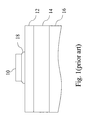
FIG. 1 shows the sensing electrode used in a conventional biopotential measurement system. In order to get over the high impedance of the Stratum Corneum 12 with bad electric conductivity, it is necessary to reduce or remove the Stratum Cornuem (including shaving of the area) or use electric conductive adhesive 18 or similar material under the sensing electrode 10 to moisten the Stratum Corneum 12 so as to enhance the conductive effect. The whole measuring effect, however, is much limited, due to drying, irritation, movement and other well documented problems. Similar or additional problems are associated with “dry” electrodes. Therefore, U.S. Pat. No. 6,334,856 discloses a microneedle device 20 shown in FIG. 2 as a sensing electrode, wherein the microneedle 22 penetrates the Stratum Corneum 12 and gets into the Stratum Germinativum 14 to measure biopotential signals. Because the Stratum Germinativum 14 consists of live cells and has a good electric conductivity, the microneedle device 20 requires no electric conductive adhesive to obtain better measuring results. Moreover, the length of the microneedle 22 can be controlled not to get into the dermis 16, hence not causing pain or bleeding to the human body. Because the microprobe has the above advantages, it has replaced the conventional sensing electrode and been widely used in the biopotential measurement systems.
When the microneedle device 20 is used as a sensing electrode, a certain external force is applied to let the microneedle 22 puncture the Stratum Corneum 12 and get into the Stratum Germinativum 14. Because the skin tissue will continually push outwards the microneedle 22 and the microneedle device 20 is of a conical shape that has a wide bottom and a narrow top and hence has no stabilization capability, the actions of the muscles under the skin will easily loosen the probe 22. Therefore, it is necessary to use a fixing tool such as adhesive tape to fix the microneedle device 20 on the skin. Since the skin tissue is very soft, the fixing effect of the microneedle device 20 varies, hence affecting the position where the probe 22 gets into the skin and making the quality of signal measurement hard to control. In consideration of this inherent problem, U.S. Pat. No. 6,690,959 discloses a microprobe structure having a probe with an inverted hooked pinpoint to let the microprobe “lodge” within the skin. But forming an inverted hook on a microprobe structure at the micrometer level is very difficult to manufacture utilizing current technique, which the patent did not disclose a feasible manufacturing method either. Although PCT Application No. WO 01/52731 discloses a process for deriving a more durable barbed spike, both probes suffer from potential breakage of the barb or damage to the skin due to probe movement caused by the barb.
Accordingly, the present invention aims to propose a microprobe array structure having a self-stabilization function and capable of measuring biopotential signals and a method for manufacturing the same.
SUMMARY OF THE INVENTION
To achieve these and other advantages and in order to overcome the disadvantages of the conventional method in accordance with the purposes of the invention as embodied and broadly described herein, the present invention provides a microprobe array structure with self-stabilization capability. The microprobe array structure can be used as a stimulus or a sensing electrode in biopotential measurement systems to measure various biopotential signals. Moreover, the drawback that the conventional microprobe array cannot be firmly stabilized in the skin tissue can be overcome.
Because the microprobe has the tip portion 34 and can puncture the Stratum Corneum 50 to get into the Stratum Germinativum 52, better electric conductivity can be obtained. Moreover, because the microprobe is self-stabilizing within the Stratum Germinativum, the biopotential measurements can be better made and/or maintained. Therefore, the microprobe won't easily loosen up in the skin tissue, and has a self-stabilization capability to overcome the drawback that the conventional microprobe array cannot be firmly stabilized in the skin tissue. Further, because the microprobe exploits the skins natural elastic/contractile property to self-stabilize; the microprobe does not anchor itself into tissue causing potential damage to the adjacent cells as with barbed spikes/probes.
Another object of the present invention is to provide a method for manufacturing a microprobe array structure. The method has a simple manufacturing process that can be easily carried out. Therefore, the manufactured microprobe array has a low cost and can be mass produced.
To achieve the above objects, the present invention provides a method for manufacturing a microprobe structure. One preferred method comprises the steps of: providing a substrate and forming a patterned masking layer thereon; isotropically etching a plurality of tip portions with the masking layer as the mask; anisotropically etching downwards a plurality of needles and controlling etching parameters to let the cross-sectional area of the connection between the needle and the tip portion be larger than that of the other end of the needle; removing the masking layer to get said microprobe structure; and forming a conducting layer on the microprobe structure. The microprobe array manufactured by the above method comprises a substrate and a plurality of microprobes. Each of the microprobes has a tip portion, a needle and a conducting layer. The top of the needle is connected to the tip portion. The bottom of the needle is connected to the substrate. The cross-sectional area of the top is larger than that of the bottom. The conducting layer covers on the tip portion and the needle. When the microprobe array is used as a sensing electrode used in the skin tissue, the substrate 30 can be connected to an external circuit to transmit the measured biopotential signals to the circuit.
BRIEF DESCRIPTION OF THE DRAWINGS
The various objects and advantages of the present invention will be more readily understood from the following detailed description when read in conjunction with the appended drawings, in which:
FIG. 1 is a diagram of a conventional sensing electrode for measuring biopotential signals;
FIG. 2 is a diagram of a conventional microprobe array used as a sensing electrode for measuring biopotential signals;
FIG. 3 is a diagram of a microprobe array of the present invention used as a sensing electrode for measuring biopotential signals
FIG. 4 is a diagram of a microprobe structure according to an embodiment of the present invention;
FIG. 5 is a diagram of a microprobe structure according to an embodiment of the present invention;
FIG. 6 is a diagram of a microprobe structure according to an embodiment of the present invention;
FIG. 7 is a diagram of a microprobe with hollow structure according to an embodiment of the present invention;
FIGS. 8( a) to 8(k) show the manufacturing steps of a microprobe array structure according to an embodiment of the present invention; and
FIG. 9( a) to 9(c) show another manufacturing steps of a microprobe array structure according to an embodiment of the present invention.
DETAILED DESCRIPTION OF THE PREFERRED EMBODIMENTS
It is the object of the present invention to provide a self stabilizing electrode suitable for mounting on the skin of a patient and which provides an improved signal to noise ratio to the bioelectrical signal obtained by the electrode. The present invention proposes an improved microprobe structure with inherent self-stabilizing features which can be used to measure various biopotential signals as electrocardiography (ECG/EKG) signals, electroencephalography (EEG) signals, electrical impedance tomography (EIT) signals, electromyography (EMG) signals and electro-oculography (EOG) signals. As used herein, the terms “biopotential”, “bioelectrical” and “biosignal” are used interchangeably and generally refer to the information received from the invention electrodes.
The microprobe electrode of the present invention reduces skin impedance and artifacts by increasing signal quality through use of microprobes to penetrate the Stratum Corneum into viable epidermis. In addition to the capability of puncturing the Stratum Corneum of the skin, the microprobe of the present invention has also the self-stabilization function in the skin tissue. Moreover, the micro-electro-mechanical manufacturing process is very stable and simple. In a preferred embodiment, as shown in FIG. 3, a microprobe array comprises a substrate 30. A plurality of microprobes is disposed on the substrate 30. Each microprobe has a tip portion 334, the bottom portion 36, and a conducting layer (not shown). The top of the needle 36 is connected to the tip portion 34, and the connection between the tip portion 34 and the bottom portion of the needle 36 has a neck 35 defined by an acute contour terminating at point 37. The base of the needle 39 is connected to the substrate 30. The cross-sectional view of the top of the needle shows the neck 35 is wider than that of the bottom of the needle 36. The conducting layer covers on the tip portion 34 and the needle 36.
In a preferred embodiment of the present invention, the microprobes tip needs to be sufficiently sharp and rigid to penetrate the skin of a patient. Although preferable, the tip portion 34, comprising the point 37 to the neck 35 of the microprobe, needs not necessarily to be of the circular or elliptical arc shape as shown in FIG. 3. The tip portion 34 can also be of the sharp angular shape shown in FIG. 4, or of the smooth shape shown in FIG. 5, or of a combination thereof, like the shape shown in FIG. 6. FIG. 7 illustrates that while the function of the microprobes may be preserved by the tip being sufficiently sharp and ending in a point, the microprobes can be made hollow to allow a drug to be passed through through-holes in substrate 30 into the microprobes responsive to pressure on the capsule, similar to many small injection needles, creating a transdermal patch/electrode. Hollow microprobes could also be employed to extract small amounts of fluids/extracts, preferably by capillary action, or small amounts of fluids could be flushed into the epidermis and could be reabsorbed for analysis of content. This could be readily employed for determination of compositional information such as glucose or other such information.
The bottom of the microprobe comprises that region between the neck 35 to the base 39 of the microprobe. A basis for self stabilization of the microprobe within the skin is based on the neck 35 having greater girth than the base 39 of the microprobe. The contraction of the skin inherently will “push” the microprobe away from the surface of the skin towards the dermis causing greater retention of the microprobe. Accordingly, the shape of the base again need not be a sharp angular shape as seen in FIGS. 3 and 4. but also of a circular or elliptical arc shape which is either concave or convex. In addition, although illustrated in FIGS. 3 and 4 as a sharp angular ridge or edge, the neck 35 of the microprobe can be beveled or circular to cause less potential damage to the cells of the skin, including for example a tear drop shape with the end being pointed, as shown in FIG. 5. In an alternative embodiment, the present invention can further comprise multiple necks 35 to further stabilize the microprobe within the skin. The base of the microprobe can be any suitable shape, including conical, spherical, pyramidal, triangular or any other such suitable shape.
Preferably, the microprobes projecting from carrier penetrate skin so that microprobe tips 34 lie within viable epidermis 50. This provides impedance reducing, electrical signal pathways across stratum corneum 52 without causing pain, discomfort or bleeding of the patient.
Accordingly, the microprobes need to be of a self-stabilizing shape sufficiently sharp and rigid to penetrate the outer layer of the skin of patient while being sufficiently elastic to prevent breaking off when exposed to lateral or bending forces and limiting the depth the microprobe will enter the skin under typical application conditions. At a minimum, the length of the spike should be greater than the depth of the Stratum Corneum 52 (ranging from 10-15 μm with a maximum of about 20 μm, unless wet) but less than the depth of the dermis 54. Preferably, the length of the microprobe ranges from about 20-800 micrometers with a more preferable length of about 20 to about 500 micrometers, most preferably a length to lie within the Stratum Basale or Stratum Germinativum, or the Stratum Spinosum, or via cross-sectional, a length within that region with living conductive cells but less than the dermis. The base 39 of each microprobe should have a radius or width less than that of the neck 35 of the microprobe. Preferably, the range of the base and neck is up to 200 micrometers wide. Microprobes may be sharp to facilitate skin penetration so that tips 34 will be substantially smaller in width than the bases 39.
Typically, the length of the microprobe will determine the depth of the penetration of the microprobe. However, other means for limiting the penetration are also contemplated whether such means are on the microprobe itself or on the substrate. For example, the microprobe can further comprise a long pin and a stop (both not shown) which will limit the depth of penetration of the microprobe. The stop can be similar to the substrate (having a single or multiple microprobes thereon) attached to a pin, such a hierarchal system facilitating microprobe penetration even on patients with hair (which would normally affect penetration depth). The pins would accommodate or account for the hair allowing penetration of the microprobe to a depth no greater than the stop. Such stops can also be on the substrate itself independent of or adjacent to the microprobes, thus limiting the depth of penetration of the microprobes, e.g., a probe having a blunt top.
The dry electrode of the present invention can be formed from a variety of processes and materials known to those skilled in the art. Other sources for materials and processes can be garnered from the semiconductor, MEMS or nanomaterials space, as well as those in biosensors. Microprobes may be manufactured from conductive material such as metal or metal alloys (for example, silver, platinum, steel or the like), electrically conductive plastic or other electroactive poymers (e.g., conductive polysaccharides such as those from bacterial sludge, seaweed or cornstarch), a semiconductor material such as silicon or doped silicon wafers, ceramics including for example oxides, and other such materials known in the art. Alternatively, microprobes could be manufactured from other materials including non-conductive materials, preferably biocompatible, more preferably, biodegradable materials, including such non-conductive materials include polymethyl methacrylate (PMMA) or poly(methyl 2-methylpropenoate), glass, and the like. Preferably, all non-conducting materials, although not limited to non-conductive materials, are coated or doped to make the electrode and/or microprobe more conductive.
As shown in FIG. 8(G), the surface of the microprobes may also be covered with a suitable material 38, such as a metal, and then coated with a suitable salt. For example, each microprobe can be coated with highly conductive plating such as silver/silver chloride layers, gold, platinum or platinum (platinum/iridium (Pt/Ir), and the like) to improve the signal to noise ratio. The metallization may be applied, after completion of standard MEMs-like knife/needle/spike construction, by vapor deposition, electrolysis, or similar metallic deposition methods. See e.g., Optimum Electrolytic Chloriding of Silver Electrodes, L. A. Geddes, L. E. Baker and A. G. Moore, Med. & Biol. Engineering, Vol. 7, Pergamon Press, 1969; Development of a platinized platinum/iridium electrode for use in vitro, K. Cote and R. Gill, Annals of Biomedical Engineering, Volume 15, Number 5 Springer Netherlands, 1987, 419-426, Electrochemical behaviour of gold, silver, platinum and palladium on the glassy carbon electrode modified by chitosan and its application, Ye X. I, Yang Q., Wang Y. and Li N., Talanta, Volume 47, Number 5, 1998, 1099-1106(8). Compounds with low electrical resistivity and biomedical compatibility are preferred and known to those of skill in the art. Other conductive layers can also be used or if the microprobes are made of a conducting material, they can be used without deposition of a conducting layer. Alternatively, the microprobes could be fashioned wherein the core of the microprobe leading to the tip is conductive, preferably flexible (e.g., wire), and the self-stabilizing component of the microprobe is nonconductive and, preferably, biocompatible/biodegradable, wherein any breakage will not cause concern of any potential contamination or injury, or the opposite, wherein the core is made of a non-conductive material and dosed with a conductive material on the exterior of the microprobe and/or electrode. In an alternate embodiment of the present invention, the microprobes could be employed to gather spectroscopic bioinformation, for example employing infrared, to determine compositional information. Each microprobe could be employed as an optic fiber to transmit/receive spectroscopic information.
In a further embodiment of the present invention, the medical electrode of the present invention comprises a substrate that includes an array of micro-dimensioned self stabilizing microprobes designed to pierce the outer skin layer, i.e. the stratum corneum and penetrate into the electrically conductive stratum germinativum, thereby to circumvent the high impedance characteristics of the stratum corneum. However, the spikes preferably will not reach the tissue layer below the stratum germinativum containing nerves and blood vessels so as to avoid pain, discomfort, or bleeding or damage to the skin or tissue. Thus, spikes that penetrate the skin more than 10-15 μm, but less than dermis, produce a pain-free electrode-electrolyte interface at the stratum germinativum and transform the ionic current induced by active cells into an electronic current. To achieve this, experiments have shown that the spike length of a majority of the spikes in the array should be in the range of 150 to 350 μm, possibly as long as 500 μm. It may be desirable to vary the length of microprobes within any given array so that measurements are obtained from various depths of the viable epidermis rather than a constant depth. Using varied lengths of microprobes is advantageous because the layers of skin vary in thickness and the skin is invariably not flat, and may also improve self-stabilizing properties of the electrode.
These microprobes are attached to a substrate in an array that allows the electrode to be applied to the surface of the human body to measure a biopotential signal, without causing pain, discomfort or damage to the skin or tissue. The shape of the microprobe array can also be a square, a circle or an irregular shape, such shape generally being dictated by the application. The microprobes can be placed throughout or interspersed on the substrate, e.g., along the edge, in patches, etc. The shape of the microprobe array will be dictated by the application and the shape of the substrate. The substrate can contain from 4-50,000 microprobes, for example in a spaced array wherein the microprobes are spaced 50-500 micrometers apart on the front side or surface of the substrate. However, it is preferable to have a microprobe density of 400 to 2,000 microprobes. The area of a substrate may be from about 2 square millimeters to about several inches, although larger areas as well as smaller areas are also contemplated depending on the application of such electrodes. Generally, the increased efficiency of the electrodes will allow the substrate to be smaller than similar electrodes, wet or dry. In one embodiment, the microprobes are interconnected and they are thus all at the same potential. In another embodiment, the microprobes are grouped to create subarrays of microprobes, e.g., a circuit board with a plurality of traces each leading to a microprobe subarray. In one embodiment, the individual microprobes or array of microprobes are used to detect cardiac depolarization directly, rather than serving as receptors of digital information. ECG tracing can be envisioned by multi-vector sensing of cardiac depolarization by proper placement of the microprobes or array of microprobes and accompanying wiring or conductivity, as opposed to the single vector sensing typically disclosed by other such skin mounted electrodes.
The substrate can be made flexible or rigid or combinations thereof. This can be based on the material of the substrate. The substrate is preferably made from the same material as microprobes, for example as a micromachined silicon chip or substantially different materials, wherein the substrate is made of such materials as fabrics, polymers, plastics, metals, semiconductor material, and the like. Alternatively, the design of the substrate can create the properties of the electrode. For example, the portions of substrate 30 not occupied by electrode areas are formed to possess a desired degree of flexibility so as to allow sensor to form to the contours of the skin of patient on which sensor is placed. A variety of techniques may be used to render these portions of substrate flexible. For example, portions may be sufficiently thin in a direction normal to the surface as to render it flexible. For material having the properties of polycarbonate plastic noted above, the thickness of portions may be less than 0.5 mm, for example, 0.2 to 0.5 mm. Or, the portions of substrate may be perforated with holes to provide the desired amount of flexibility to portion.
An electrical interconnection of the front side and backside of the electrode must be established either directly through substrate or through the exterior of substrate. In one embodiment, a through-hole or holes can be fabricated and both sides substrate coated with a conductive material. By paying special attention that the front side and backside conductive layer coating overlap, the necessary electrical connection may be made between microprobes and lead wire or port. Or, the connection may be obtained by overlapping conductive coatings along the edges of the substrate 30.
An electrical connection between electrode and a bioelectrical monitor or terminal (not shown) may be achieved by a number of various means known in the art, including wireless and wired means. For practical purposes, electrode may be provided with a projecting terminal, e.g., a clip or snap or other similar connector terminal residing on substrate 30, preferably on the side of substrate, as an extension to substrate or on the backside of electrode (i.e., side opposite to microprobes). This allows the electrode to be readily replaceable and disposable, irrespective of whether wired or unwired to the monitor or terminal. Accordingly, leads may connect one or several electrodes to the monitor or terminal using a clip-connector mating to terminal. The information can be transmitted with wires or leads, or alternatively, wireless technologies, including Bluetooth™, ZigBee™, or other proprietary or non-proprietary wireless format, including wireless formats approved for medical use. Those of skill will readily recognize alternative wireless technologies applicable in the present invention to transmit single channel or multi-channel information
Electrical leads are attached between the electrode and a monitor or terminal so that the biopotential, or other such information, obtained from the electrode may be analyzed and/or amplified for display or recording. A still further object of the present invention is to provide an electrode which can amplify weak bioelectrical or other such signals. In yet another embodiment of the present invention, an amplifier and battery are attached to the electrode to boost the signal obtained from the subject. The amplifier is not activated until the electrode is in use. This activation may be started by removing a protective tape from the battery and circuitry. A still further object of the present invention is to provide a terminal to analyze and/or display the biosignals. The terminal can be any device which can receive the information and/or display the information, including electronic, graphical, written or printed display such as on PCs, portable devices such as watches, cell-phones and PDAs, print-outs, and other medical and consumer devices typically employed for display, storage and analysis of medical electronic information such as EEG, EKG/ECG, EMG, EOG, and EIT. Other devices and applications will be readily known to those of skill in the art.
Another object of the present invention is to provide such an electrode which may be used without preparing the skin prior to application, and which does not require paste or gels. Although it is contemplated that the electrode will be self secured against the skin once initial pressure is placed on the electrode on the skin, the electrode can be further embodied with means to further stabilize the electrode on the body. The bioelectrode may be kept in position using an adhesive tape or an adhesive on the periphery of the carrier, such as an electrolytic adhesive may be disposed on the underside of the carrier. If desired, the electrode can be used with a conductive gel located between the skin and the carrier, although it may be preferably for the electrode to be used dry. If conductive gel is used (typically held in place with a retainer net or screen material, or such other means known in the art), it may contain antibacterial agents to prevent irritation or infection due to spike penetration of the skin. An electrolytic gel or paste is used in conjunction with an electrode so constructed to make movement artifact less prominent and improve the signal to noise ratio.
Prior to use, microprobes may be protected by a protective paper or film and other suitable means and/or the electrode placed in suitable packaging. The protective paper or film is removed from electrode immediately before the electrode is applied to the patient's skin. Electrode is applied to skin by firmly pressing down on the entire surface of bioelectrode, toward the patient's skin. This pressing action causes microprobes to engage and penetrate skin. The electrical leads are then attached to the electrodes as previously described, and to the bioelectrical monitor that records or displays bioelectrical signals.
The electrode of the present invention can be formed from a variety of processes known to those skilled in the art. These include the general processes typically employed for MEMS or nanomaterial or biosensor devices, including micromachining and semiconductor device manufacturing processes. Current semiconductor processes are now being exploited to develop medical devices and such processes can be readily applied in the current invention process, including deposition, removal, patterning and modification of electrical properties as generally applied in the semiconductor industry. Deposition is any process that grows, coats, or otherwise transfers a material onto the wafer. Available technologies consist of physical vapor deposition (PVD), chemical vapor deposition (CVD), electrochemical deposition (ECD) or similar electroplating techniques, molecular beam epitaxy (MBE) and more recently, atomic layer deposition (ALD) among others. Removal processes are any that remove material from the wafer either in bulk or selective form and consist primarily of etch processes, both wet etching and dry etching such as reactive ion etch (RIE) (also, see, e.g., deep reactive ion etching (DRIE) process). Chemical-mechanical planarization (CMP) is also a removal process used between levels. Patterning covers the series of processes that shape or alter the existing shape of the deposited materials and is generally referred to as lithography. For example, in conventional lithography, the wafer is coated with a chemical called a “photoresist.” The photoresist is exposed by a “stepper”, a machine that focuses, aligns, and moves the mask, exposing select portions of the wafer to short wavelength light. The unexposed regions are washed away by a developer solution. After etching or other processing, the remaining photoresist is removed by plasma ashing. Modification of electrical properties has historically consisted of doping transistor sources and drains originally by diffusion furnaces and later by ion implantation. These doping processes are followed by furnace anneal or in advanced devices, by rapid thermal anneal (RTA) which serve to activate the implanted dopants. Modification of electrical properties now also extends to reduction of dielectric constant in low-k insulating materials via exposure to ultraviolet light in UV processing (UVP). Different processing steps are also well known to those in the art including front and back end processing and growth of gate dielectrics, Plasma ashing, thermal treatments such as rapid thermal anneal, furnace anneals and oxidation, wafer/device/IC testing, die preparation, packaging steps and other similar steps.
The fabrication of needles extending from the plane of a silicon wafer has been reported in the technical literature. See for example Micromachined Needles for the Transdermal Delivery of Drugs, S. Henry, D. V. McAllister, M. G Allen, and M. R. Prausnitz, Proceedings IEEE Micro Electro Mechanical Systems, 1998; Novel AFM Probes-Fabrication and Characterization, Anja Boisen, Ole Hansen and Siebe Bowastra, Micro Structure Workshop, 1998; and Micromachined, Silicon Based Electrode Arrays for Electrical Stimulation of or Recording from Cerebral Cortex, Richard A. Norman, Patrick K. Campbell and Kelly E. Jones, Proceedings IEEE Micro Electro Mechanical Systems, 1991.
FIGS. 8( a) to 8(k) show one preferred embodiment of the manufacturing steps of the above microprobe array. As shown in FIG. 8( a), a silicon substrate 30 is first provided. A patterned masking layer 32 made of photoresist or thin film material is then defined out on the silicon substrate 30 by means of photolithography, as shown in FIG. 8( b). Next, as shown in FIG. 8( c), a plurality of conical tip portions is isotropically etched with said masking layer as the mask. As shown in FIGS. 8( d) and 8(e), a plurality of needles is anisotropically etched downwards, and etching parameters are controlled to let the ratio of the cross-sectional areas of the connection between the tip portion 34 and the needle 36 and the other end of the needle 36 be larger than 1. Moreover, the connection between the tip portion 34 and the needle 36 has edges and corners or other shapes capable of enhancing the friction between the microprobe and the skin to enhance the stabilization capability of the microprobe. The isotropic and anisotropic etching can be dry etching or wet etching. Subsequently, after the masking layer 32 is removed by means of dry etching or wet etching to get the microprobe structure shown in FIG. 8( f), a conducting layer 38 is formed on the microprobe structure to enhance the electric conductivity of the microprobe for sensing physiologic signals, as shown in FIG. 8( g). The material of the conducting layer 38 is selected among polymer, thin film material and metal. The microprobe array is thus formed.
Because the conducting layers 38 of the microprobes are connected together, this microprobe array can only be used to measure one kind of biopotential signal. Alternatively, various film layers, specific coatings and leads can be coated or deposited onto the electrode to make it individually addressable or to function as desired in an (sub)array. Or the electrode can be doped to increase the conductivity of the electrode.
In order to expand the function of the microprobe array, one preferred embodiment of the present invention further proposes a novel design in which part of the conducting layer 39 on the substrate is removed to electrically isolate the microprobes. After the step of FIG. 8( g), a photoresist layer 40 is formed on the plurality of microprobes, as shown in FIG. 8( h). A mask is then formed and a routing 42 is defined out by means of exposure, as shown in FIG. 8( i). Next, the conducting layer outside the microprobe and the routing 42 is removed, as shown in FIG. 8( j). Finally, the photoresist layer 40 is removed to get the microprobe structure with mutually isolated microprobes, as shown in FIG. 8( k). Because the conducting layers between the microprobes are mutually isolated, each microprobe can be separately connected to a different measuring circuit by pulling out the corresponding routing 42. Therefore, the microprobe array can be used for the measurement of various kinds of biopotential signals, and can also be used as stimuli. The whole microprobe array can be used as sensing ends or stimuli, or part of the microprobe array is used as sensing ends while other part of the microprobe array is used as stimuli. When some microprobes are used as stimuli, voltages or currents will be conducted into the microprobes to electrify them; or the microprobes are not electrified but only puncture the skin to render pressure to the punctured location. Other microprobes used as sensing ends are responsible for sensing the stimulation result.
One alternative process contemplated to form the electrode is to form the invention electrode by an additive deposition process. Preferably, an electroplating process is used. Preferably, the substrate for this process is a flexible polymer, and more preferably an insulating polymer such as a polyimide. With this process a thin layer of metal is applied to the substrate. Then a thick layer of photo resist is applied to the thin layer of metal on the substrate and patterned by photolithography to create the desired features, i.e., arrays of squares, circles, etc. These patterns form the base of the electrodes and the other features of the electrode array. The photo resist is stripped from the substrate. Another layer of photoresist is applied. These patterns further define the microprobe structure which is built up to the desired height and shape by electroplating. Optionally, at this point various film layers and leads can be coated onto the electrode to make it individually addressable or to function to improve the conductivity as desired in an array of electrodes.
Yet another invention process is where the electrode can be formed from metal sheet through photo micro-machining techniques, e.g., photo and/or chemical etching, laser machining, abrasion and other metal working techniques are applied on a thin gauge stock of metal to produce the microprobes and the electrode. An array can be better formed by stacking and laminating.
Yet another invention process is to create the electrode by injection molding, casting or depositing a material into a mold. As shown in FIG. 9( a), a mold 60 with the imprint or negative image of the desired surface features which may include the microprobes and substrates, as well as any additional features is formed. In FIG. 9( b), this mold 60 may be filled via injection molding, casting, deposition or other material forming technique to produce the desired electrode 62. Optionally and as a function of the conductivity of the material utilized, as shown in FIG. 9( c), the surface may be doped to increase the conductivity of the electrode, and also various film layers and leads can be coated onto the electrode 62 to make it individually addressable or to function as desired in an array of electrodes.
Those of skill in the art will readily recognize additional processes which can be applied in forming invention electrodes. In addition to functionality of the electrode, those of skill in the art will readily recognize that other attributes, such as cost, availability of electrode materials and fabrication materials, ease of manufacture, regional and regulatory concerns, biocompatibility, acceptance by industry, and other such factors will dictate the fabrication of the invention electrode.
The electrodes of the present invention can be used in a variety of applications including but not limited to ECG, EEG, EIT, EMG, and EOG. The electrodes can be packaged by conventional packaging techniques, however, preferably the package provides 1) adequate structural support for the electrode so it can be handled roughly (i.e., dropped, crushed, etc) without damage; 2) a means (i.e., a spring, etc) to force the electrode against the subjects skin with a consistent pressure; 3) a low impedance path from the electrodes surface to the package's output connector; 4) a design which allows for easy cleaning and sterilization for applications requiring reuse; 5) a design to allow disposability of electrode and/or packaging; 6) a design to easily activate or expose electrode; and 7) a design to allow the user to readily determine prior use and/or other such safety and cross-contamination concerns, including infection.
The dry physiological recording electrodes are applied to an animal or human body having skin comprising an epidermis comprising a stratum corneum layer and lower layers of the epidermis, and a dermis. The microprobes(s) of the electrode pierce through the stratum corneum layer of the skin with the microprobe(s) such that the microprobe(s) does not enter the dermis of the skin. When attached to the skin of the subject, microprobe(s) obtains biopotential signals or provides electrostimulation of body tissue. The microprobe(s) senses the ionic current in the lower layers of the epidermis, and transforms a portion of the ionic current of the lower layers of the epidermis of the skin into an electric voltage through the microprobe(s). The electric voltage from the microprobe(s) is measured using conventional measuring devices.
The electrode of the present invention may also be used to enhance the administration of skin applied drugs. To this end, a drug container, such as a flexible capsule, may be provided on the backside of the electrode. A plurality of through-holes may be provided in substrate to discharge the drug to the skin of the subject when the flexible capsule is pressed. The penetration of the skin by the spikes facilitates passage of the drug through the stratum corneum. The length of the microprobes in such an application also should be the same as for electrodes without such feature thus inflicting no pain to the patient. The drug delivery can be combined with electrical stimulation.
To sum up, the present invention provides two microprobe structures (one with electrically connected microprobes and the other with electrically isolated microprobes) and their manufacturing methods. Moreover, the microprobes of these two structures have the self-stabilization capability in the skin tissue. Because the substrate of the microprobe array of the present invention is silicon, a very high supporting force in the longitudinal direction can be provided, and the shrinkage of the bottom of the needle 36 has little influence to the longitudinally exerted force of the structure. Besides, because the Stratum Corneum 50 and the Stratum Germinativum 52 of the skin will come off themselves due to metabolism, it is not necessary to worry about that the probe may be remained in the skin. The length of the microprobe array (i.e., the total length of the tip portion 34 and the needle 36, about 240˜450 micrometers) is designed in accordance with the human race or age range to be measured, it won't get into the dermis 54 to cause pain or bleeding to the measured person.
Although the present invention has been described with reference to the preferred embodiments thereof, it will be understood that the invention is not limited to the details thereof Various substitutions and modifications have been suggested in the foregoing description, and other will occur to those of ordinary skill in the art. Therefore, all such substitutions and modifications are intended to be embraced within the scope of the invention as defined in the appended claims.

Claims (33)

1. A microprobe structure used to measure biopotential signals, said microprobe structure comprising:
an elongated tapering needle member having an increasing width in a first section integrally formed with a second section, said second section having an acute contour terminating at a point to define a tip portion; and
a conducting layer covering said needle member including said tip portion.
2. The microprobe structure as claimed in claim 1, wherein said tip portion is conical.
3. The microprobe structure as claimed in claim 1, wherein said tip portion can puncture the Stratum Corneum and Stratum Germinativum to allow said microprobe to get into said Stratum Germinativum and measure said biopotential signals.
4. The microprobe structure as claimed in claim 1, wherein said biopotential signals include electroencephalographic (EEG) signals, electrocardiographic (ECG) signals and electromyographic (EMG) signals.
5. The microprobe structure as claimed in claim 1, wherein the total length of said tip portion and said needle member is 250˜450 micrometers.
6. The microprobe structure as claimed in claim 1, wherein a connection between said tip portion and a remaining portion of said needle member includes edges and corners to enhance a stabilization capability of said microprobe.
7. The microprobe structure as claimed in claim 1, wherein a ratio of a cross-sectional area at an interface between said tip portion and a remaining portion of said needle member and a bottom of said needle member is larger than 1.
8. The microprobe structure as claimed in claim 1, wherein the material of said conducting layer is polymer, thin film material or metal.
9. The microprobe structure as claimed in claim 1, wherein a bottom of said needle member is connected to a substrate and used as a sensing electrode that is connected to an external circuit and used to receive said measured biopotential signals.
10. The microprobe structure as claimed in claim 9, wherein the material of said substrate is silicon.
11. The microprobe structure as claimed in claim 9, wherein a plurality of said microprobes is disposed on said substrate to form a microprobe array.
12. The microprobe structure as claimed in claim 11, wherein said conducting layers of said microprobes are connected together to measure one of said biopotential signals.
13. The microprobe structure as claimed in claim 11, wherein said conducting layers of said microprobes are mutually isolated, and said microprobe array is used to measure a plurality of said biopotential signals.
14. The microprobe structure as claimed in claim 13, wherein each of said microprobes with mutually isolated conducting layers is used as a stimulus.
15. The microprobe structure as claimed in claim 14, wherein when said microprobe is used as a stimulus, a voltage or a current is conducted into said microprobe to electrify said microprobe or render pressure to the punctured location.
16. The microprobe structure as claimed in claim 11, wherein the shape of said microprobe array is a square, a circle, or an irregular shape.
17. The microprobe structure as claimed in claim 1, wherein the needle member including the tip portion is hollow.
18. A microprobe array structure used to measure biopotential signals, said microprobe array structure comprising:
a substrate; and
a plurality of microprobes each having an elongated tapering needle member having an increasing width in a first section integrally formed with a second section, said second section having an acute contour terminating at a point to define a tip portion, and a bottom of said needle member being connected to said substrate, wherein a conducting layer coats said needle member including said tip portion.
19. The microprobe array structure as claimed in claim 18, wherein said tip portion is conical.
20. The microprobe array structure as claimed in claim 18, wherein said tip portion can puncture the Stratum Corneum and Stratum Germinativum to allow said microprobe to get into said Stratum Germinativum and measure said biopotential signals.
21. The microprobe array structure as claimed in claim 18, wherein said biopotential signals include electroencephalographic (EEG) signals, electrocardiographic (ECG) signals and electromyographic (EMG) signals.
22. The microprobe array structure as claimed in claim 18, wherein the total length of said needle member including said tip portion is 250˜450 micrometers.
23. The microprobe array structure as claimed in claim 18, wherein a connection between said tip portion and a remaining portion of said needle member includes edges and corners to enhance a stabilization capability of said microprobe.
24. The microprobe array structure as claimed in claim 18, wherein a ratio of a cross-sectional area at an interface between said tip portion and a remaining portion of said needle member and a bottom of said needle member is larger than 1.
25. The microprobe array structure as claimed in claim 18, wherein the material of said conducting layer is polymer, thin film material or metal.
26. The microprobe array structure as claimed in claim 18, wherein said substrate is used as a sensing electrode that is connected to an external circuit and used to receive said measured biopotential signals.
27. The microprobe array structure as claimed in claim 18, wherein the material of said substrate is silicon.
28. The microprobe array structure as claimed in claim 18, wherein said conducting layers of said plurality of microprobes are connected together to measure one of said biopotential signals.
29. The microprobe array structure as claimed in claim 18, wherein said conducting layers of said plurality of microprobes are mutually isolated, and said microprobe array is used to measure a plurality of said biopotential signals.
30. The microprobe array structure as claimed in claim 29, wherein each of said microprobes with mutually isolated conducting layers is used as a stimulus.
31. The microprobe array structure as claimed in claim 30, wherein when said microprobe is used as a stimulus, a voltage or a current is conducted into said microprobe to electrify said microprobe or render pressure to the punctured location.
32. The microprobe array structure as claimed in claim 18, wherein a shape of each of said plurality of microprobes is a square, a circle, or an irregular shape.
33. The microprobe array structure as claimed in claim 18, wherein the microprobe is hollow.
US11/599,303 2006-06-09 2006-11-15 Microprobe array structure and method for manufacturing the same Expired - Fee Related US7941201B2 (en)

Applications Claiming Priority (3)

Application Number Priority Date Filing Date Title
TW95120528 2006-06-09
TW95120528A 2006-06-09
TW095120528A TW200744534A (en) 2006-06-09 2006-06-09 Microprobe array structure and manufacturing method thereof

Publications (2)

Publication Number Publication Date
US20080009763A1 US20080009763A1 (en) 2008-01-10
US7941201B2 true US7941201B2 (en) 2011-05-10

Family

ID=38919931

Family Applications (1)

Application Number Title Priority Date Filing Date
US11/599,303 Expired - Fee Related US7941201B2 (en) 2006-06-09 2006-11-15 Microprobe array structure and method for manufacturing the same

Country Status (2)

Country Link
US (1) US7941201B2 (en)
TW (1) TW200744534A (en)

Cited By (26)

* Cited by examiner, † Cited by third party
Publication number Priority date Publication date Assignee Title
US20080294031A1 (en) * 2007-05-22 2008-11-27 Persyst Development Corporation Method and device for quick press on eeg electrode
US20100222630A1 (en) * 2006-01-17 2010-09-02 Emkinetics, Inc. Method and apparatus for low frequency induction therapy for the treatment of urinary incontinence and overactive bladder
US20110295100A1 (en) * 2010-05-28 2011-12-01 Hegde Anant V Microneedle electrode
US20120265046A1 (en) * 2006-12-08 2012-10-18 General Electric Company Self-adhering electrodes and methods of making the same
US20130197338A1 (en) * 2012-01-30 2013-08-01 Electronics And Telecommunications Research Institute Pain signal measurement device and pain signal measuring and controlling method thereof
US8574295B2 (en) 2012-01-17 2013-11-05 Vista Ocular, Llc Accommodating intra-ocular lens system
US8594763B1 (en) * 2010-05-25 2013-11-26 Neurowave Systems Inc. Physiological electrode assembly for fast application
US8666484B2 (en) 2011-11-25 2014-03-04 Persyst Development Corporation Method and system for displaying EEG data
US8694070B2 (en) 2007-05-22 2014-04-08 Persyst Development Corporation Electrode applicator for quick press on EEG electrode
US20140107458A1 (en) * 2011-05-18 2014-04-17 Katholieke Universiteit Leuven, KU LEUVEN R&D Resilient Sensor for Biopotential Measurements
US20140275911A1 (en) * 2013-03-13 2014-09-18 Advanced Semiconductor Engineering, Inc. Neural sensing device and method for making the same
US9002477B2 (en) 2006-01-17 2015-04-07 Emkinetics, Inc. Methods and devices for performing electrical stimulation to treat various conditions
US9005102B2 (en) 2006-10-02 2015-04-14 Emkinetics, Inc. Method and apparatus for electrical stimulation therapy
US9055927B2 (en) 2011-11-25 2015-06-16 Persyst Development Corporation User interface for artifact removal in an EEG
US9173583B2 (en) * 2013-03-15 2015-11-03 Advanced Semiconductor Engineering, Inc. Neural sensing device and method for making the same
US9339641B2 (en) 2006-01-17 2016-05-17 Emkinetics, Inc. Method and apparatus for transdermal stimulation over the palmar and plantar surfaces
US9610459B2 (en) 2009-07-24 2017-04-04 Emkinetics, Inc. Cooling systems and methods for conductive coils
US9770207B2 (en) 2013-12-23 2017-09-26 Verily Life Sciences Llc Sensor electrodes in a bio-compatible device
US10321858B2 (en) 2014-08-18 2019-06-18 Proteadx, Inc. Apparatus and methods for transdermal sensing of analytes in interstitial fluid and associated data transmission systems
US10702375B2 (en) 2015-09-18 2020-07-07 Vista Ocular, Llc Electromyographic sensing and vision modification
US10786669B2 (en) 2006-10-02 2020-09-29 Emkinetics, Inc. Method and apparatus for transdermal stimulation over the palmar and plantar surfaces
US10929753B1 (en) 2014-01-20 2021-02-23 Persyst Development Corporation System and method for generating a probability value for an event
US11219416B2 (en) 2018-03-12 2022-01-11 Persyst Development Corporation Graphically displaying evoked potentials
US11224742B2 (en) 2006-10-02 2022-01-18 Emkinetics, Inc. Methods and devices for performing electrical stimulation to treat various conditions
US11317871B2 (en) 2011-11-26 2022-05-03 Persyst Development Corporation Method and system for detecting and removing EEG artifacts
US11457855B2 (en) 2018-03-12 2022-10-04 Persyst Development Corporation Method and system for utilizing empirical null hypothesis for a biological time series

Families Citing this family (38)

* Cited by examiner, † Cited by third party
Publication number Priority date Publication date Assignee Title
TW200921109A (en) * 2007-11-09 2009-05-16 Univ Nat Chiao Tung Assembly structure of 3D probe array
WO2009135200A2 (en) * 2008-05-02 2009-11-05 Aspect Medical Systems, Inc. Skin preparation device and biopotential sensor
TWI475978B (en) * 2009-01-17 2015-03-11 Ind Tech Res Inst Dry electrode and manufacturing method thereof
US9295417B2 (en) 2011-04-29 2016-03-29 Seventh Sense Biosystems, Inc. Systems and methods for collecting fluid from a subject
US9119578B2 (en) 2011-04-29 2015-09-01 Seventh Sense Biosystems, Inc. Plasma or serum production and removal of fluids under reduced pressure
JP6078230B2 (en) 2009-03-02 2017-02-08 セブンス センス バイオシステムズ,インコーポレーテッド Techniques and devices related to blood sampling
TWI373324B (en) * 2009-05-05 2012-10-01 Univ Nat Chiao Tung Biomedical sensor
US8795504B2 (en) * 2009-08-27 2014-08-05 University Of Southern California Electrodeposition of platinum/iridium (Pt/Ir) on Pt microelectrodes with improved charge injection properties
TWI481383B (en) * 2009-09-25 2015-04-21 Univ Nat Chiao Tung Biosensor and electrode structure thereof
US8707734B2 (en) * 2009-10-19 2014-04-29 The Regents Of The University Of Michigan Method of embedding material in a glass substrate
US8834423B2 (en) * 2009-10-23 2014-09-16 University of Pittsburgh—of the Commonwealth System of Higher Education Dissolvable microneedle arrays for transdermal delivery to human skin
US20130158482A1 (en) * 2010-07-26 2013-06-20 Seventh Sense Biosystems, Inc. Rapid delivery and/or receiving of fluids
US8855736B2 (en) * 2010-08-05 2014-10-07 Richard A. Jaffe Safety transcutaneous electrode
WO2012021801A2 (en) 2010-08-13 2012-02-16 Seventh Sense Biosystems, Inc. Systems and techniques for monitoring subjects
JP5044685B2 (en) * 2010-09-10 2012-10-10 株式会社東芝 Microprobe, recording apparatus, and method of manufacturing microprobe
WO2012046231A2 (en) * 2010-10-04 2012-04-12 Nervomatrix Ltd. Electrode for finding points of low impedance and applying electrical stimulation thereto
US20130158468A1 (en) 2011-12-19 2013-06-20 Seventh Sense Biosystems, Inc. Delivering and/or receiving material with respect to a subject surface
EP2701600B1 (en) 2011-04-29 2016-06-08 Seventh Sense Biosystems, Inc. Delivering and/or receiving fluids
TWI481384B (en) * 2012-04-02 2015-04-21 Univ Chung Hua Bio probe assembly
JP2015515886A (en) 2012-05-01 2015-06-04 ユニバーシティ オブ ピッツバーグ − オブ ザ コモンウェルス システム オブ ハイヤー エデュケイション Tip-loaded microneedle array for percutaneous insertion
WO2014120114A1 (en) * 2013-01-29 2014-08-07 Empire Technology Development Llc Microneedle-based natremia sensor and methods of use
US10390724B2 (en) * 2013-06-26 2019-08-27 The Penn State Research Foundation Three-dimensional bio-medical probe sensing and contacting structures with addressibility and tunability
WO2015021333A1 (en) * 2013-08-07 2015-02-12 Cornell Universty Semiconductor tweezers and instrumentation for tissue detection and characterization
WO2016126253A1 (en) 2015-02-05 2016-08-11 The Penn State Research Foundation Nano-pore arrays for bio-medical, environmental, and industrial sorting, filtering, monitoring, or dispensing
US10441768B2 (en) 2015-03-18 2019-10-15 University of Pittsburgh—of the Commonwealth System of Higher Education Bioactive components conjugated to substrates of microneedle arrays
WO2017066768A1 (en) 2015-10-16 2017-04-20 University Of Pittsburgh-Of The Commonwealth System Of Higher Education Mullti-component biio-active drug delivery and controlled release to the skin by microneedle array devices
WO2017120322A1 (en) 2016-01-05 2017-07-13 University Of Pittsburgh-Of The Commonwealth System Of Higher Education Skin microenvironment targeted delivery for promoting immune and other responses
US11058337B2 (en) * 2017-02-03 2021-07-13 International Business Machines Corporation Flexible silicon nanowire electrode
GB201709668D0 (en) * 2017-06-16 2017-08-02 Spts Technologies Ltd Microneedles
US11324429B2 (en) * 2019-01-29 2022-05-10 Forest Devices, Inc. Headgear having electrodes integrally formed therein having a gel distribution apparatus
US10940554B2 (en) 2018-11-30 2021-03-09 International Business Machines Corporation Planar fabrication of micro-needles
WO2020152628A2 (en) * 2019-01-23 2020-07-30 Wyss Center For Bio And Neuro Engineering Tissue access device
WO2021062476A1 (en) * 2019-10-01 2021-04-08 WearOptimo Pty Ltd Analyte measurement system
US11266476B1 (en) 2021-04-07 2022-03-08 Forest Devices, Inc. Headgear storage device and method of distribution
USD1018861S1 (en) 2021-04-07 2024-03-19 Forest Devices, Inc. Headgear
USD970019S1 (en) 2021-04-07 2022-11-15 Forest Devices, Inc. Gel distribution module
US11241182B1 (en) 2021-04-07 2022-02-08 Forest Devices, Inc. Gel distribution apparatus and method
CN115444426B (en) * 2022-11-09 2023-04-28 之江实验室 On-chip electrode integrated wireless myoelectricity SoC system, chip and acquisition device

Citations (7)

* Cited by examiner, † Cited by third party
Publication number Priority date Publication date Assignee Title
US6091975A (en) * 1998-04-01 2000-07-18 Alza Corporation Minimally invasive detecting device
US6334856B1 (en) 1998-06-10 2002-01-01 Georgia Tech Research Corporation Microneedle devices and methods of manufacture and use thereof
US20020082543A1 (en) * 2000-12-14 2002-06-27 Jung-Hwan Park Microneedle devices and production thereof
US6622035B1 (en) 2000-01-21 2003-09-16 Instrumentarium Corp. Electrode for measurement of weak bioelectrical signals
US6690959B2 (en) 2000-09-01 2004-02-10 Medtronic, Inc. Skin-mounted electrodes with nano spikes
US20040054393A1 (en) 2000-01-21 2004-03-18 Goran Stemme Medical electrode
US6782283B2 (en) 2001-09-07 2004-08-24 Robert N. Schmidt Dry penetrating recording device

Patent Citations (7)

* Cited by examiner, † Cited by third party
Publication number Priority date Publication date Assignee Title
US6091975A (en) * 1998-04-01 2000-07-18 Alza Corporation Minimally invasive detecting device
US6334856B1 (en) 1998-06-10 2002-01-01 Georgia Tech Research Corporation Microneedle devices and methods of manufacture and use thereof
US6622035B1 (en) 2000-01-21 2003-09-16 Instrumentarium Corp. Electrode for measurement of weak bioelectrical signals
US20040054393A1 (en) 2000-01-21 2004-03-18 Goran Stemme Medical electrode
US6690959B2 (en) 2000-09-01 2004-02-10 Medtronic, Inc. Skin-mounted electrodes with nano spikes
US20020082543A1 (en) * 2000-12-14 2002-06-27 Jung-Hwan Park Microneedle devices and production thereof
US6782283B2 (en) 2001-09-07 2004-08-24 Robert N. Schmidt Dry penetrating recording device

Non-Patent Citations (1)

* Cited by examiner, † Cited by third party
Title
P. Griss, P. Enoksson, H.K. Tolvanen-Laakso, P. Merilainen, S. Ollmar, G. Stemme, "Micromachined Electrodes for Biopotential Measurements", J. of Microelectromechanical System, vol. 10, No. 1, 2001.

Cited By (46)

* Cited by examiner, † Cited by third party
Publication number Priority date Publication date Assignee Title
US9002477B2 (en) 2006-01-17 2015-04-07 Emkinetics, Inc. Methods and devices for performing electrical stimulation to treat various conditions
US20100222630A1 (en) * 2006-01-17 2010-09-02 Emkinetics, Inc. Method and apparatus for low frequency induction therapy for the treatment of urinary incontinence and overactive bladder
US9757584B2 (en) 2006-01-17 2017-09-12 Emkinetics, Inc. Methods and devices for performing electrical stimulation to treat various conditions
US9630004B2 (en) 2006-01-17 2017-04-25 Emkinetics, Inc. Method and apparatus for transdermal stimulation over the palmar and plantar surfaces
US9387338B2 (en) 2006-01-17 2016-07-12 Emkinetics, Inc. Methods and devices for performing electrical stimulation to treat various conditions
US9339641B2 (en) 2006-01-17 2016-05-17 Emkinetics, Inc. Method and apparatus for transdermal stimulation over the palmar and plantar surfaces
US10786669B2 (en) 2006-10-02 2020-09-29 Emkinetics, Inc. Method and apparatus for transdermal stimulation over the palmar and plantar surfaces
US11844943B2 (en) 2006-10-02 2023-12-19 Emkinetics, Inc. Method and apparatus for transdermal stimulation over the palmar and plantar surfaces
US11628300B2 (en) 2006-10-02 2023-04-18 Emkinetics, Inc. Method and apparatus for transdermal stimulation over the palmar and plantar surfaces
US9005102B2 (en) 2006-10-02 2015-04-14 Emkinetics, Inc. Method and apparatus for electrical stimulation therapy
US11224742B2 (en) 2006-10-02 2022-01-18 Emkinetics, Inc. Methods and devices for performing electrical stimulation to treat various conditions
US11247053B2 (en) 2006-10-02 2022-02-15 Emkinetics, Inc. Method and apparatus for transdermal stimulation over the palmar and plantar surfaces
US20120265046A1 (en) * 2006-12-08 2012-10-18 General Electric Company Self-adhering electrodes and methods of making the same
US8626258B2 (en) * 2006-12-08 2014-01-07 General Electric Company Self-adhering electrodes and methods of making the same
US8694070B2 (en) 2007-05-22 2014-04-08 Persyst Development Corporation Electrode applicator for quick press on EEG electrode
US20080294031A1 (en) * 2007-05-22 2008-11-27 Persyst Development Corporation Method and device for quick press on eeg electrode
US8112141B2 (en) * 2007-05-22 2012-02-07 Persyst Development Corporation Method and device for quick press on EEG electrode
US8185183B1 (en) * 2007-05-22 2012-05-22 Persyst Development Corporation Method and device for quick press on EEG electrode
US20120136230A1 (en) * 2007-05-22 2012-05-31 Persyst Development Corporation Method and device for quick press on eeg electrode
US8271065B1 (en) 2007-05-22 2012-09-18 Persyst Development Corporation Method and device for quick press on EEG electrode
US9610459B2 (en) 2009-07-24 2017-04-04 Emkinetics, Inc. Cooling systems and methods for conductive coils
US20150018657A1 (en) * 2010-05-25 2015-01-15 Stéphane Bibian Physiological electrode assembly for fast application
US9050015B2 (en) * 2010-05-25 2015-06-09 Neuro Wave Systems Inc. Physiological electrode assembly for fast application
US11039774B1 (en) * 2010-05-25 2021-06-22 NeuroWave Systems, Inc. Physiological electrode assembly for fast application
US8594763B1 (en) * 2010-05-25 2013-11-26 Neurowave Systems Inc. Physiological electrode assembly for fast application
US9901278B1 (en) * 2010-05-25 2018-02-27 Neurowave Systems Inc Physiological electrode assembly for fast application
US8805469B1 (en) * 2010-05-25 2014-08-12 Neurowave Systems Inc Physiological electrode assembly for fast application
US8588884B2 (en) * 2010-05-28 2013-11-19 Emkinetics, Inc. Microneedle electrode
US20110295100A1 (en) * 2010-05-28 2011-12-01 Hegde Anant V Microneedle electrode
US20140107458A1 (en) * 2011-05-18 2014-04-17 Katholieke Universiteit Leuven, KU LEUVEN R&D Resilient Sensor for Biopotential Measurements
US9055927B2 (en) 2011-11-25 2015-06-16 Persyst Development Corporation User interface for artifact removal in an EEG
US8666484B2 (en) 2011-11-25 2014-03-04 Persyst Development Corporation Method and system for displaying EEG data
US11317871B2 (en) 2011-11-26 2022-05-03 Persyst Development Corporation Method and system for detecting and removing EEG artifacts
USRE46615E1 (en) 2012-01-17 2017-11-28 Vista Ocular, Llc Accommodating intra-ocular lens system
US8574295B2 (en) 2012-01-17 2013-11-05 Vista Ocular, Llc Accommodating intra-ocular lens system
US20130197338A1 (en) * 2012-01-30 2013-08-01 Electronics And Telecommunications Research Institute Pain signal measurement device and pain signal measuring and controlling method thereof
US9089268B2 (en) * 2013-03-13 2015-07-28 Advanced Semiconductor Engineering, Inc. Neural sensing device and method for making the same
US20140275911A1 (en) * 2013-03-13 2014-09-18 Advanced Semiconductor Engineering, Inc. Neural sensing device and method for making the same
US9173583B2 (en) * 2013-03-15 2015-11-03 Advanced Semiconductor Engineering, Inc. Neural sensing device and method for making the same
US9770207B2 (en) 2013-12-23 2017-09-26 Verily Life Sciences Llc Sensor electrodes in a bio-compatible device
US10929753B1 (en) 2014-01-20 2021-02-23 Persyst Development Corporation System and method for generating a probability value for an event
US11803753B1 (en) 2014-01-20 2023-10-31 Persyst Development Corporation Apparatus and product of manufacture for generating a probability value for an event
US10321858B2 (en) 2014-08-18 2019-06-18 Proteadx, Inc. Apparatus and methods for transdermal sensing of analytes in interstitial fluid and associated data transmission systems
US10702375B2 (en) 2015-09-18 2020-07-07 Vista Ocular, Llc Electromyographic sensing and vision modification
US11219416B2 (en) 2018-03-12 2022-01-11 Persyst Development Corporation Graphically displaying evoked potentials
US11457855B2 (en) 2018-03-12 2022-10-04 Persyst Development Corporation Method and system for utilizing empirical null hypothesis for a biological time series

Also Published As

Publication number Publication date
US20080009763A1 (en) 2008-01-10
TW200744534A (en) 2007-12-16
TWI328441B (en) 2010-08-11

Similar Documents

Publication Publication Date Title
US7941201B2 (en) Microprobe array structure and method for manufacturing the same
EP1164928B1 (en) Method of fabricating a medical electrode
US7881764B1 (en) Physiological recording device
US6782283B2 (en) Dry penetrating recording device
Neuman Biopotential electrodes
US6622035B1 (en) Electrode for measurement of weak bioelectrical signals
US8700122B2 (en) Skin preparation device and biopotential sensor
US8626258B2 (en) Self-adhering electrodes and methods of making the same
US6961603B2 (en) Unitary multi-electrode biopotential signal sensor and method for making same
US8112139B2 (en) Skin screw electrode
US10959632B1 (en) Physiological recording device or electrode
KR101785287B1 (en) Microneedle electrode patch and fabrication method of the microneedle electrode patch
Ghane-Motlagh et al. A review of microelectrode array technologies: design and implementation challenges
US7286864B1 (en) Dry physiological recording device

Legal Events

Date Code Title Description
AS Assignment

Owner name: NATIONAL CHIAO TUNG UNIVERSITY, TAIWAN

Free format text: ASSIGNMENT OF ASSIGNORS INTEREST;ASSIGNORS:CHIOU, JIN-CHERN;HUNG, CHEN-CHUN;CHANG, CHIH-WEI;REEL/FRAME:018559/0258

Effective date: 20061030

STCF Information on status: patent grant

Free format text: PATENTED CASE

FPAY Fee payment

Year of fee payment: 4

FEPP Fee payment procedure

Free format text: MAINTENANCE FEE REMINDER MAILED (ORIGINAL EVENT CODE: REM.); ENTITY STATUS OF PATENT OWNER: SMALL ENTITY

LAPS Lapse for failure to pay maintenance fees

Free format text: PATENT EXPIRED FOR FAILURE TO PAY MAINTENANCE FEES (ORIGINAL EVENT CODE: EXP.); ENTITY STATUS OF PATENT OWNER: SMALL ENTITY

STCH Information on status: patent discontinuation

Free format text: PATENT EXPIRED DUE TO NONPAYMENT OF MAINTENANCE FEES UNDER 37 CFR 1.362

FP Lapsed due to failure to pay maintenance fee

Effective date: 20190510