US7945880B1 - Constraint based retiming of synchronous circuits - Google Patents
Constraint based retiming of synchronous circuits Download PDFInfo
- Publication number
- US7945880B1 US7945880B1 US11/755,425 US75542507A US7945880B1 US 7945880 B1 US7945880 B1 US 7945880B1 US 75542507 A US75542507 A US 75542507A US 7945880 B1 US7945880 B1 US 7945880B1
- Authority
- US
- United States
- Prior art keywords
- retiming
- circuit
- node
- clock period
- computed
- Prior art date
- Legal status (The legal status is an assumption and is not a legal conclusion. Google has not performed a legal analysis and makes no representation as to the accuracy of the status listed.)
- Active, expires
Links
Images
Classifications
-
- G—PHYSICS
- G06—COMPUTING; CALCULATING OR COUNTING
- G06F—ELECTRIC DIGITAL DATA PROCESSING
- G06F30/00—Computer-aided design [CAD]
- G06F30/30—Circuit design
- G06F30/32—Circuit design at the digital level
- G06F30/33—Design verification, e.g. functional simulation or model checking
- G06F30/3308—Design verification, e.g. functional simulation or model checking using simulation
- G06F30/3312—Timing analysis
-
- G—PHYSICS
- G06—COMPUTING; CALCULATING OR COUNTING
- G06F—ELECTRIC DIGITAL DATA PROCESSING
- G06F2119/00—Details relating to the type or aim of the analysis or the optimisation
- G06F2119/12—Timing analysis or timing optimisation
Definitions
- the embodiments of the invention relate generally to retiming integrated circuit netlists during logic synthesis. More particularly, the embodiments of the invention relate to constraint based retiming with boundaries to maximize forward movement of flip-flops.
- logic cells from a cell library are mapped into a netlist to begin the physical design process of an integrated circuit.
- logic gates in a data path are often separated by D-type flip flops during the logic synthesis process. Oftentimes the logic gates are conservatively placed between D-type flip flops such that the timing delays can easily beat out the given clock period. However, this leads to overly conservative designs that are not area efficient. Retiming the logic gates in a data path by moving the flip flops forward or backward to eliminate one or more flip flops can conserve area in an integrated circuit design that can lead to a reduced die size with reduced manufacturing costs.
- retiming is used to improve the performance (e.g., cycle time) of the integrated circuits.
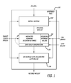
- FIG. 1 is a block diagram of a synthesis tool in accordance with an embodiment of the invention.
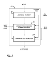
- FIG. 2 is a block diagram of a placement tool in accordance with another embodiment of the invention.
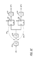
- FIGS. 3A-3C are exemplary schematic circuit diagrams to illustrate circuit retiming.
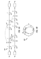
- FIG. 4A is an exemplary bounds retiming graph to illustrate circuit retiming.
- FIG. 4B is an exemplary register-to-register graph.
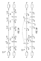
- FIGS. 5A-5B are exemplary retiming graphs with possible arrival times and retiming values for each node being illustrated in FIG. 5A .
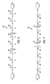
- FIG. 6 is an exemplary retiming graph to show how iteratively bounding of the retiming values may occur.
- FIG. 7 is an exemplary retiming graph representing a retiming of a circuit that not only minimizes the maximum delay but also balances out the slack.
- FIGS. 8A-8B are flow charts illustrating a method of circuit retiming in accordance with embodiments of the invention.
- FIG. 9 illustrates an exemplary computing system that may be used to perform some or all of the processes in accordance with a number of embodiments of the invention.
- the embodiments of the invention include a method, apparatus and system for constraint based retiming of synchronous circuits.
- Retiming is a structural netlist transformation which moves registers forward and backward in the logic. Retiming has the objective to (1) minimize the clock period and to (2) minimize the number of registers either for the minimum clock period achievable by retiming or for a given clock period.
- Registers can have different control signals and may also have initial states (reset line). Registers which have different control signals cannot be combined when they are moved forward (in the direction of the signal propagation) or backward over a gate. Similarly, registers with initial states cannot be moved backward over a gate if the justification problem does not have a solution. This leads to a constrained retiming problem. For each node in a retiming graph, what are the constraints on the number of flops which can be moved forward or backward over the respective node.
- the minimum clock period which can be achieved by retiming is found by a binary search over the clock period and a successive check if a clock period is feasible. Generating the network flow problem for the feasibility test and for minimizing the register count is the most CPU intensive part. Hence, it is important to have a good lower and upper bound on the clock period.
- a first embodiment of the invention is a methodology to compute lower and upper bounds of the clock period where the difference between the lower and upper bound is substantially at most the maximum delay of a gate. That is, constraints are considered when computing retiming values to quickly determine a solution.
- the first embodiment of the invention addresses the problem of efficiently computing a good lower and upper bound on the clock period achievable for the constrained retiming problem. Good lower and upper bounds on the clock period are important to efficiently find the minimum clock period which can be realized by retiming.
- the problem of finding a retiming that minimizes the number of registers for a given clock period can be formulated and solved as a network flow problem. It is possible to bound the retiming values of nodes and determine that the retiming values of some nodes are fixed by solving the clock scheduling problem with clock latencies as large as possible (ALAP) and with clock latencies as small as possible (ASAP).
- the clock latency problem computes latencies of the clock signal, that is, the delay from the clock root to the clock input of a register.
- the ALAP/ASAP approach is described in “Efficient retiming of large circuits”, by N. Maheshwari and S.
- a second embodiment of the invention iteratively uses the initial bounds of the retiming values to derive even stronger bounds for the retiming values of the nodes, that is, the number of registers moved backward over a node (negative number means forward). If the stronger bounds are infeasible for a given clock period, then the clock period cannot be realized by retiming. By using stronger bounds for the retiming values, more variables and constraints in the network flow formulation can be eliminated and runtime of logic synthesis can be further improved.
- the second embodiment of the invention iteratively bounds the retiming values of the nodes.
- the embodiments of the invention may be incorporated into a number of electronic computer aided design (ECAD) software tools to perform circuit retiming.
- ECAD electronic computer aided design
- the synthesis tool 100 is a software program includes software modules.
- One of the software modules of the synthesis tool is a mapper 102 to initially map a high level description (RTL/HDL) of an integrated circuit into an initial netlist using a target clock period and circuit cells of a cell library.
- a retimer 104 of the synthesis tool 100 retimes the netlist with minimized forward register retiming in response to the target clock period and the gate delays of the instantiated gates in the initial netlist and bounded retiming values.
- the retimer 104 may further exaggerate the gate delays of the instantiated cells with a gate delay exaggerator 106 before or after performing the retiming.
- the gate delay exaggerator 106 implements delay factors for the respective logic gates that are instantiated in the netlist. The delay factors for logic gates are further described below.
- a re-mapper 108 remaps the netlist with the exaggerated gate delays to generate the retimed netlist in response to the target clock period and the cells of the cell library.
- the placement tool 200 includes a placer 202 to incrementally place cells of a cell library into a layout of the integrated circuit design in response to a netlist thereof.
- a retimer 204 of the placement tool 200 receives the layout and incrementally retimes the netlist with minimized forward register retiming in response to the target clock period and the gate delays of the gates placed into the layout and the bounded retiming values.
- a logic optimizer 206 of the placement tool 200 may incrementally optimize the layout design. For example, the logic optimizer 206 may resize an output buffer due to the parasitic impedance loading in order to meet timing requirements.
- the logic optimizer 206 may add a buffer to a node in order to meet the timing requirements and buffer a parasitic impedance load.
- the incremental logic optimization performed by the optimizer 206 is responsive to the target clock period, the instantiated layouts of the cells from the cell library, and the gate delays of the instantiated cells in the layout.
- the incremental placement, retiming, and optimization is repeated over and over again for sequential logic in data paths between registers for a functional block or a plurality of functional blocks in the integrated circuit design. That is, retiming is a global optimization technique.
- Retiming is a powerful technique for delay and area minimization.
- the registers are moved forward and backward across logic gates.
- the technique was first proposed in “Optimizing Synchronous Systems” by C. Leiserson and J. Saxe, Journal of VLSI and Computer Systems, Vol. 1, pp 41-67, January 1983, and “Retiming synchronous Systems” by C. Leiserson and J. Saxe, Algorithmica, Vol. 6, pp 5-35, 1991, which are both incorporated herein by reference and referred to as “Leiserson and Saxe”.
- Leiserson and Saxe considered two versions of the retiming problem. The first was a minimum period retiming problem in which the registers are relocated to minimize the clock period. The second was a minimum area retiming problem in which a target clock period is given and the registers are then relocated to minimize the total number of registers subject to the given clock period.
- a linear programming formulation is disclosed which takes constraints on the retiming value into account. This is fundamentally different from a clock scheduling problem as it does not work with a register-to-register graph but directly with a retiming graph.
- retiming values can be directly computed without having to iteratively move the registers to determine retiming.
- special solutions of the linear programs may be used to derive bounds on the retiming values.
- a circuit can be modeled as an edge-weighted, node-weighted, directed (multi-) graph (referred to as a retiming circuit graph or simply as a retiming graph).
- the nodes are the primary inputs (PIs), the primary outputs (POs), and the logic gates of the circuit.
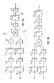
- FIG. 4A illustrates an exemplary retiming graph with primary inputs PIA and PIB, primary outputs POA and POB, registers A through C, and logic gates represented by circuit symbols.
- the interconnections between nodes are edges “e”. For example, an edge between nodes u and v may be referenced by e uv .
- a given node v representing a logic gate
- the fanin is represented by fanin edges and the function FI(v) represents the number of fanin edges of a node v.
- the fanout of a given node v is represented by fanout edges and the function FO(v) represents the number of fanout edges.
- the nonnegative weight d(v) of a node v represents the propagation delay of the corresponding gate at the node.
- the weight w(e uv ) of an edge e uv is the number of registers on the interconnection between nodes.
- Retiming a node may be achieved by a forward movement of registers in the same direction of signal propagation or a backward movement of registers opposite the direction of signal propagation.
- backward movement of registers also referred to as “backward register movement”
- a retiming of a node by a value i is an operation that moves i registers from each fanout edge and adds i registers to each fanin edge of the node. We say the register is moved backward (opposite) and the value of i is positive.
- a retiming of a node by a value i takes i registers from each fanin edge and adds i registers to each fanout edge of the node.
- a negative value of i indicates that registers are moved forward during retiming from the fanin edges of a node to the fanout edges of the node.
- the nodes in a circuit can be retimed collectively.
- FIGS. 3A-3B illustrate a forward register retiming movement.
- a circuit includes D-flip flops or registers 301 - 305 and logic blocks 311 - 316 coupled together between inputs IN 1 -IN 2 and an output OUT 1 as shown.
- Arrows 320 - 321 illustrated forward movement of registers 302 and 305 to perform retiming and eliminate a register. Forward register movement is usually preferable over backward register movement due to the ease of handling set, reset, or other control signals at the registers.
- FIG. 3B illustrates the instantiation of register 307 in place of registers 302 and 305 .
- FIG. 3A further illustrates the forward movement of register 303 in front of the logic block 316 .
- FIG. 3B illustrates the instantiation of register 309 in front of the logic block 316 in place of register 303 .
- the logic blocks 315 - 316 are now between registers 307 and 309 .
- retiming preserves functionality when the retiming values for the primary inputs (PI) and the retiming values for the primary outputs (PO) are zero.
- r be a retiming of a circuit where r(v) is the retiming value of a node v, r(u) is the retiming value of a node u, and w(e uv ) is the weight of an edge e uv in the initial circuit. If the retiming value r(u) of the node u is positive there is backward register movement. If the retiming value r(u) of the node u is negative there is forward register movement.
- a retiming that results in nonnegative edge weights w r (e uv ) is called a legal retiming.
- the clock period of a circuit is the maximum delay on the combinational paths (paths without registers) in the circuit.
- a circuit can be retimed to a clock period T if a legal retiming exists for which the retimed circuit has the clock period of at most T. If a legal retiming does not exist or if the clock period of the retimed circuit is greater than T, a circuit can not be retimed.
- W and D that are defined for all pairs of nodes (u,v) for which a u-v-path exists.
- W(u,v) denotes the minimum number of registers on all u-v-paths and D(u,v) is the maximum delay of all u-v-paths which have the minimum number of registers.
- the minimum area retiming problem which minimizes the number of registers for a given clock period T was formulated by Leiserson and Saxe as the following linear program (LP2), which also may be referred to as a minimized area retiming program: min(
- the first constraint ensures that after retiming the number of registers of every edge is nonnegative (w r (e) ⁇ 0).
- the edge weight w(e uv ) for each pair of nodes of the initial circuit is greater than or equal to the difference between the retiming values r(u) and r(v).
- the second constraint ensures that there is at least one register on every u-v-path for which the total delay D(u,v) along the u-v-path is greater than or equal to the given target clock period T.
- the linear program LP2 is the dual of a network flow problem which can be solved efficiently by a polynomial time algorithm.
- a retiming solution is sought to achieve the best possible clock period. That is, the smallest T is sought out for which the linear program LP2 has a solution.
- a solution to the linear program is sought which minimizes the clock period as a first criteria and also minimizes the number of registers as a second criteria. This is achieved by performing a binary search over the clock period T and successively checking if a solution for the linear program LP2 exists. In order to efficiently perform the binary search a good lower and upper bound on the best possible clock period is required.
- the weight d(e) of the edge e represents the maximum propagation delay out of all the paths from the register u to the register v.
- the register u at node u has its own latency or delay l(u) with respect to the clock in generating data at its output.
- the problem to minimize the clock period T by clock latency scheduling can be formulated as the following linear program (LP3), which may be referred to herein as register graph clock scheduling program: min T such that l ( u )+ d (( u,v )) ⁇ T ⁇ l ( v ) ⁇ ( u,v ) ⁇ E (3)
- the optimum clock period achievable by clock latency scheduling gives a lower bound on the clock period which can be obtained by retiming.
- the computed clock latencies can be used to retime the circuit.
- the registers with a positive clock latency l(u) are moved backward.
- the registers with a negative clock latency l(u) are moved forward. Sapatnekar and Deokar show that the final clock period of the resulting retiming is not larger than the clock period achievable with the clock latencies plus the maximum delay of all gates, hence this gives a good upper bound.
- a clock latency scheduling was used to further improve the runtime of the minimum area retiming problem for a given clock period (referred to as a “Minaret algorithm”).
- Two clock latency schedules were computed.
- the first clock latency schedule was computed with latencies as small as possible (ASAP), the second schedule with latencies as large as possible (ALAP).
- ASAP small as possible
- ALAP the second schedule with latencies as large as possible
- the first solution results in a retiming where all registers are moved forward by as much as possible and similarly the second solution results in a retiming where all registers are moved backward by as much as possible.
- lower and upper bounds on the retiming values r of the nodes can be derived. This helps to eliminate a good portion of the variables in the minimized area retiming program (2) and of the period constraints.
- a clock signal and a data signal may be all that is coupled into each flip flop of a register.
- a system may have a plurality of different clock signals such that different clock signals are coupled into various registers.
- different clock signals may be coupled into each functional block such that selective portions of a system corresponding to one or more functional blocks may have their clocks turned when inactive to conserve power.
- Registers may be classified differently into different register classes based upon the clock signal that they receive.
- registers require initialization or further control and receive some other control signals.
- the registers not only receive a clock signal but they also receive a control signal.
- a register may have a load enable signal that differs from other registers.
- a register may have a synchronous or an asynchronous set and/or reset signal coupled to each flip-flop that are controlled differently by differing control signals. Registers may be further classified differently into different register classes based upon the control signals that they receive.
- registers are assigned to differing register classes. All registers in the same register class receive the same clock and control signals. As the registers are moved forward and backward in the combinational logic, only registers of the same class are combined together during the retiming process. Registers in different register classes are not combined together during the retiming process. For example, negative edge triggered registers in one register class are not merged together with positive edge triggered registers during the retiming process.
- registers that are initialized to an initial state add to the complexity of the retiming of a circuit. This is the case when registers are set or reset to an initial state in one position and are moved during the retiming process. What are the required reset/set values for registers when they are moved to a new location in the data path curing retiming.
- the resultant output of a register at its original position in response to the original set/reset values need to be propagated through the combinational logic to the new position of the register and a new set/reset value needs to be determined for the register in the new position. This is particularly problematic when registers are moved backward in the combinational logic, such that a justification problem has to be solved.
- registers 335 and 336 may be moved backward over the logic L 2 332 and merged into one new register.
- the outputs of the register 335 and register 336 are initialized to different states (e.g., the output of the register 305 is initialized to logical zero and the output of the register 306 is initialized to logical one), then moving the two registers backward over the gate L 2 332 creates a justification problem.
- the new register the result of merging the two backward moving registers, can only be initialized to one logical value. Propagating the initialized value to the original locations of the registers should result in the given initialized values.
- the outputs of the register 335 and register 336 are initialized to different states, the registers cannot be retimed backward in this example and the circuit cannot be retimed. In contrast moving registers of the same register class forward and merging them together is always possible. The reset values are just propagated forward as the registers are moved.
- registers with initial states are moved only forward. However, a set of registers at the primary outputs may be removed and placed back at the primary inputs.
- registers are iteratively moved forward as far as possible to obtain a lower bound r l (v) ⁇ 0 on the retiming value r(v) for each node.
- a lower bound on the retiming value constrains the forward movement of registers.
- the registers are iteratively moved backward as far as possible to obtain an upper bound r u (v) ⁇ 0 on the retiming value r(v).
- the embodiments of the invention search for a legal retiming r with a minimum clock period subject to the constraint r l (v) ⁇ r(v) ⁇ r u (v) for all v ⁇ V.
- FIG. 4A shows an exemplary retiming graph 400 A of a circuit.
- FIG. 4B illustrates a register-to-register graph 400 B of the same circuit.
- the retiming graph 400 A of the circuit there are a plurality of nodes 401 - 410 and registers RA-RC between two primary inputs PIA,PIB and two primary outputs POA,POB. Associated with each of the nodes 401 - 410 is a delay indicated above each. Assume that the registers RA and RB receive different control signals and belong to different register classes. Thus, registers RA and RB cannot be combined together and retimed forward over the node x 407 because they are in different register classes.
- the clock period is determined by the by the path from register RB to the primary output POB as register RB cannot be moved forward.
- the total delay from register RB to POB is 26. Because there is only one register along the path from RB to POB, the clock period may not be smaller than 26/2 or 13. Thus, the optimal clock period which can be achieved by retiming in the circuit is thirteen.
- Register RC may be moved backward one node over node 409 to a position RC′ during the retiming process for example.
- Register RA may be moved forward one node over node 402 to position RA′ just before node x 407 and duplicated and moved forward two nodes over node 402 - 403 to a position RA′′ between nodes 403 and 404 during the retiming process.
- the duplicated register RA′′ may be moved further forward over node 404 but in this case rests between nodes 403 and 404 to minimize register movement.
- the delay between a register RA′′ and the primary output POA is ten.
- the delay between the primary input PIA and register RA′′ is ten.
- the delay from register RA′′ to the primary output POA is ten.
- the delay from registers RA′ and RB to register RC′ is thirteen.
- the delay from register RC′ to the primary output POB is thirteen.
- the delay from the primary input PIA to the register RA′ is two.
- the delay from the primary input PIB to register RB remains 4.
- the timing delay is one. From the I/O node to the register node RB, the timing delay is 4. From the register node RA to the I/O node, the timing delay is 19. From the register node RA to the register node RC, the timing delay is 17. From the register node RB to the register node RC the timing delay is 16. From the register node C to the I/O node, the timing delay is 10.
- Clock latency scheduling may be performed with the register-to-register graph 400 B assuming that all registers are in the same register class by ignoring the constraint that the two registers RA and RB are in different register classes.
- register RA can only be moved forward in the direction of node X 407 over one node, node 402 which has a delay of one time unit, to position RA′. If we add a lower bound of ⁇ 1 time unit to the clock latency of register RA in FIG. 4B , we would get a clock period of 18 between register RA and register RB that is still not a lower bound on the clock period. Thus, it is not possible to achieve a good lower and upper bound on the clock period by using clock latency scheduling on a register-to-register graph in the presence of constraints on the retiming values, such as a constraint due to different register classes.
- a linear program for retiming circuits is now formulated which takes the lower and upper bounds on the retiming values into account and still provides a lower bound on the clock period.
- the methodology of the linear program efficiently handles the constraints due to the different register classes.
- an arrival time variable a(v) is defined for every node v in the circuit.
- the arrival time variable a(v) represents the arrival time of the data signal at the gate input pins of the logic gate corresponding to the node v for the initial circuit that has yet to be retimed.
- the arrival time variable a r (v) represents the arrival time of the data signal at the gate input pins of the logic gate corresponding to the node v in the retimed circuit.
- the vector of the arrival times a(v) for all vertices or nodes v in the set V i.e., v ⁇ V
- (a(v)) v ⁇ V The vector of the arrival times a(v) for all vertices or nodes v in the set V (i.e., v ⁇ V) is denoted by (a(v)) v ⁇ V .
- each edge e uv has a weight of d(u) ⁇ w(e uv )T r .
- a cycle of edges is positive (“positive cycles”) if the sum of the weights of the cycle is positive.
- a circuit retimed with a legal retiming r has a feasible clock period T r if there is a solution to following system of inequalities:
- a linear program LP5 for the retiming graph referred to as a constrained minimum period retiming arrival time program, can be formulated:
- the optimal solution of the constrained minimum period retiming arrival time program provides a lower bound for the constrained minimum period retiming problem. It can also shown how a solution of the constrained minimum period retiming arrival time program can be converted into a retiming which has a clock period no greater than the minimized T solution of the constrained minimum period retiming arrival time program plus the maximum delay of all gates in the circuit.
- the arrival time variables a(v), v ⁇ V can be interpreted as arrival times.
- the arrival time variables can be negative or largely positive, possibly greater than the clock period.
- the embodiments of the invention disclosed herein do not work with a register-to-register graph but a retiming graph. Moreover, the retiming is computed directly in the embodiments of the invention based on arrival times without an interative register movement process.
- the set of inequality equations for the constrained minimum period retiming arrival time program is a special type.
- An additional arrival time variable a(h) for a host node h can be added to the left side of the second inequality and similarly to the right side of the third inequality. We can assume that the arrival time variable a(h) for the host node is zero.
- each inequality has one of the variable a(v), v ⁇ V ⁇ h ⁇ on the left side and on the right side as shown:
- the objective variable T may be subtracted once or several times depending upon the value of r l (v) and upper r u (v).
- This form of linear program LP6 may be solved with a Bellman-Ford algorithm using a binary search over the variable ⁇ and testing for a negative cycle each time.
- the system of inequalities of LP6 has a solution if and only if the graph does not have a negative cycle.
- linear program LP6 may be solved directly with an extension of the parametric shortest paths (PSP) algorithm described in “Faster Parametric Shortest Path and Minimum Balance Algorithms,” by N. E. Young, R. E. Tarjan, and J. B. Orlin, Networks , vol. 21, no. 2, pp. 205-221, 1991, incorporated herein by reference (hereafter referred to as “Young, Tarjan, and Orlin”).
- PSP parametric shortest paths
- n the number of variables
- m the number of inequalities
- C the maximum parameter p(i,j) of the inequalities.
- the value of C is bounded by the maximum number of registers on any primary input to primary output path and on any cycle in the retiming graph.
- the number of operations required by the parametric shortest paths algorithm by Young, Tarjan and Orlin (cited previously) to find a solution to the linear program LP6 can be bounded by K(nm+Cn 2 log n), where K is a constant.
- the linear program has many more variables to deal with.
- the register-to-register graph for the clock scheduling problem may contain substantially more edges corresponding to constraints. That is, the number of edges in a register-to-register graph that need computing may be greater than the number of edges in a retiming graph.
- the arrival time at each node in the retimed circuit is equal to the difference of the respective arrival time in the initial circuit and the product of the clock period with the respective retimed value for each node, and the clock period T r is equal to the sum of the clock period and the maximum gate delay.
- the number of period constraints is reduced in the network flow formulation for minimizing the number of registers.
- the number of period constraints is reduced by computing upper and lower bounds on the retiming values and determining which nodes if any, for which a retiming value has already been determined.
- an upper bound and a lower bound on retiming values may be further used to determine if a retiming can achieve a feasible clock period or not.
- the upper bounds and the lower bounds of the retiming values for each node may be computed from a solution of the constrained minimum period retiming arrival time program (LP5) respectively with arrival times (a(v)) v ⁇ V as large as possible (i.e., the largest arrival times) and arrival times (a(v)) v ⁇ V as small as possible (i.e., the smallest arrival times).
- LP5 constrained minimum period retiming arrival time program
- This inequality provides an upper bound on the retiming value r(v) if (a(v)) v ⁇ V is a solution for the constrained minimum period retiming program (LP5) in which the arrival times (a(v)) v ⁇ V are as large as possible.
- an exemplary retiming graph 500 A is illustrated with possible arrival times and retiming values for each node corresponding to the exemplary retiming graph 500 B of FIG. 5B .
- the possible arrival times and retiming values are indicated below each node with the retiming values enclosed by parenthesis.
- the node x 407 has the constraint that its retiming value being greater than or equal to zero (i.e., r(x) ⁇ 0) because registers RA and RB cannot be combined and moved forward over node x 407 . This means that registers may be moved backward over node x 407 so that its retiming r(x) is positive.
- the lower bound on the retiming value of node x 407 results in constraint for the arrival times at node x 407 being greater than or equal to zero (i.e., a(x) ⁇ 0).
- the retiming values of the nodes in parenthesis are determined so that a legal retiming may be found.
- the retiming values are less than or equal to the rounded down value of the quotient of the arrival time at the respective node divided by the clock period.
- the retiming value of node 409 is determined by dividing its arrival time 13 by the clock period 13 and rounding down if need be.
- the retiming value of node 409 is one (1).
- the retiming value of node 404 is the arrival time ⁇ 3 divided by the clock period 13 which is a negative fraction ( ⁇ 3/13) that is further rounded down to a retiming value of minus one ( ⁇ 1).
- the retiming value of node 404 is the arrival time ⁇ 12 divided by the clock period 13 which is a negative fraction ( ⁇ 12/13) that is further rounded down to minus one ( ⁇ 1).
- the retiming value of node 408 is the arrival time 4 divided by the clock period 13 which is a positive fraction (4/13) that is further rounded down to zero (0).
- register RA may be moved forward over nodes 402 - 404 to position RA′′′ along the path from PIA to POA and no further because each of nodes 402 - 404 has a negative one retiming value and the retiming value of node 405 is zero.
- Register RA is duplicated and moved forward over node 402 to position RA′ along the path from PIA to POB and no further as node 402 has a negative one retiming value and node 407 has a retiming value of zero. This is the case as the fanout from node 402 is greater than one. Register RB does not move over either node 406 or 407 as their respective retiming values are zero. Register RC moves backward over node 409 along the path from PIA to POA and no further to position RC′ as the retiming value of node 409 is positive one and the retiming value of node 408 is zero.
- the upper and lower bound inequalities may be combined together to form the range over which the retiming values for each node are bounded.
- the lower and upper bounds on the retiming value may be determined from equation 10 as follows. Let ( ⁇ (v)) v ⁇ V , be a solution for the linear inequalities in the constrained minimum period retiming program (LP5) for a given clock period T with the arrival times ⁇ (v) as large as possible for every v ⁇ V. Similarly, let ( a (v)) v ⁇ V , be a solution for the linear inequalities of the constrained minimum period retiming program (LP5) with arrival times a (v) as small as possible for every v ⁇ V. Then for any retiming r which achieves the clock period T, the following inequality holds:
- a lower bound on the clock period for the constrained retiming problem may be computed with given upper and lower bounds on the retiming values. Additionally, new lower and upper bounds on the retiming values may be computed given arrival times as small as possible for each node and arrival times as large as possible for each node, respectively. The newly computed upper and lower bounds on the retiming values are usually stronger than the given bounds and may be used to determine that a certain given clock period cannot be achieved by a retiming, as was discussed previously. With this in mind, a path in a circuit may have its retiming values iteratively bounded to determine feasibility or infeasibility of retiming the circuit.
- FIG. 6 an exemplary retiming graph is illustrated for iteratively bounding the retiming values.
- FIG. 6 shows a path from a primary input PI to a primary output PO with eight gates represented by the nodes v 1 601 through v 8 608 and two registers R 1 , R 2 on the edges (v 3 ,v 4 ) and (v 5 ,v 6 ).
- the numbers above each node is the gate delay of each gate at the node.
- the lower bound on the clock period is computed by solving the constrained minimum period retiming arrival time program.
- the constraint r(v 3 ) ⁇ 1 results in the constraint a(v 3 ) ⁇ T and the constraint r(v 6 ) ⁇ 1 results in the constraint a(v 6 )+4 ⁇ 0 for the constrained minimum period retiming arrival time program.
- the computing process may be reiterated with a new possible feasible clock period.
- the lower bound on the clock period may be used as a new possible feasible clock period to achieve a retiming of the circuit.
- Circuit retimings with certain desired properties can be found. For example, a retiming can be quickly found in accordance with the embodiments of the invention for which the movement of the registers in the circuit is minimized. With retimings of circuits being quickly found with the embodiments of the invention, they can be repeatively performed to find a more desired retiming. Additionally, a retiming can be computed in which the maximum delay of all combinational paths is minimized but in which most paths have a delay not greater than a given target clock period. This may be used in determining the critical path of the circuit design.
- delay factors are introduced to exaggerate the gate delay of each gate in a data path.
- minimizing the number of registers can be extremely CPU expensive. This is especially the case if the given clock period is large, such as from a critical area in the circuit design.
- a large clock period can increase the number of period constraints in the network flow formulation and the computations performed for retiming a circuit.
- a retiming can be made that minimizes the clock period, moves registers rather forward than backward (good for the justification problem for registers with initial states) and keeps registers as close as possible to their original or initial location.
- the constrained minimum period retiming arrival time program (LP5) may be solved with a possibly feasible clock period.
- the phrase possibly feasible clock period may also be referred to herein as a potential clock period.
- a solution of the constrained minimum period retiming arrival time program (LP5) is computed with all arrival times (a′(v)) v ⁇ V being as small as possible using the Dijkstra's shortest path algorithm (cited previously).
- the constrained minimum period retiming arrival time program (LP5) is modified to
- the modified constrained minimum period retiming arrival time program (LP5X) is solved with a possibly feasible clock period.
- a fast retiming methodology such as this for a circuit may be found in a matter of several minutes whereas a retiming to minimize the number of registers in the same circuit may take an hour or more to compute.
- a circuit design typically has a critical part or critical path which determines the minimum clock period achievable by circuit retiming.
- the minimum clock period achievable by circuit retiming turns out to be substantially larger than the desired target clock period. If there is such a critical part or path in a circuit design, a designer should know that it may cause problems during circuit retiming. If the retiming is to only minimize the delay of a long path, many combinational paths may have the same delay after the circuit is retimed as a result.
- a retiming to additionally minimize the number of registers along the long path for the target clock period may not be useful and could also be extremely CPU intensive, causing significant delay in generating a retimed circuit.
- the constrained minimum period retiming arrival time program may be extended or the modified constrained minimum period retiming arrival time program (LP5X) may be further extended to alleviate the problems that might be caused by a critical part or a critical path in a circuit design.
- the extended constrained minimum period retiming arrival time program is to look for a circuit retiming in which most paths have the delay of a given target clock period T g , while the minimum clock period T achievable by retiming is greater. That is T>T g .
- An optimization problem can be formulated to achieve this.
- a delay factor ⁇ (v) is introduced.
- a gate delay exagerator 106 may generate the delay factors ⁇ (v) for each gate.
- the delay factors ( ⁇ (v)) v ⁇ V are feasible for a clock period T and a retiming r if the retimed circuit, in which every gate v has a delay of ⁇ (v)d(v), can run with a clock period of T.
- the retimed circuit can achieve a clock period of T. Furthermore, if the value of the delay factor is at least
- T T g for every gate or node in the solution of the linear program (LP6), then the retimed circuit can achieve a clock period T of T g +D.
- a solution is sought to the linear program (LP6) in which every gate has a delay factor of at least one and in which “many” gates have a delay factor of at least the fraction
- T T g which is greater than one, if the clock period T is greater than the target clock period T g or T>T g .
- This is referred to as a balanced delay factor maximization or balanced slack factor maximization.
- a solution is sought in which the vector of the delay factors ordered in increasing order (smallest factor first) is as large as possible by lexicographic order.
- the solution can be found by a sequence of linear programs introducing one variable for all the delay factors and maximizing the variable.
- a solution for which this variable is maximum has a cycle of tight inequality constraints. The value of these constraints may be fixed and then the variable can be maximized once again.
- the balanced slack factor maximization problem can be solved efficiently with the minimum mean balance algorithm described in “Faster Parametric Shortest Path and Minimum Balance Algorithms,” by Young, Tarjan, and Orlin (cited previously).
- an exemplary retiming graph 700 is illustrated representing a retiming of a circuit that not only minimizes the maximum delay but also balances out the slack.
- the retiming graph 700 has a simple data path from a primary input (PI) to a primary output (PO) with two registers R 1 and R 2 coupled there-between as shown.
- the nodes 701 - 708 represent logic gates.
- the delay factors ⁇ (v) for each gate are the delay factors ⁇ (v) for each gate.
- the delay factor ⁇ (v) for nodes 701 - 704 is one for example.
- the delay factors ⁇ (v) for nodes 705 - 708 is two for example.
- the minimum clock period which can be achieved with retiming is 4 tu.
- the delay factor ⁇ (v) has a value of one for nodes 701 - 704 and is maximized first.
- four nodes 701 - 704 from the primary input PI to the first register provides a delay of 4 tu equivalent to the minimum clock period.
- the delay factors are all 1.0, whereas for the gates following the first register R 1 the delay factors are 2.0.
- the second register R 2 is placed in the middle between the first register R 1 and the primary output PO such that the edges (paths) between registers R 1 and R 2 and register R 2 and the primary output PO have a delay of 2 tu balancing out the delay.
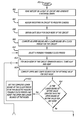
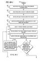
- FIGS. 8A-8B a flow chart of a method for retiming a circuit is illustrated. The method starts at block 801 and then goes to block 802 .
- a netlist and/or layout of an initial circuit is read and an initial structure of a retiming graph may be generated in response to the netlist and any parasitics that may be extracted from the layout.
- the flip-flops and registers are detected and gates along data paths are assigned to nodes with routing defining edges between nodes and registers.
- the algorithms described previously work well with a retiming graph of a circuit.
- registers in the circuit are assigned to their respective register classes.
- the register class into which a register is assigned may be dependent upon the clock signals and control signals that may be coupled to the registers in the circuit.
- the gate delay for each node of the circuit is obtained.
- the gate delay may be read from a technology file for a cell library or it may be determined based upon a circuit simulation of one or more gates that may be assigned to a node.
- an upper bound and a lower bound of a clock period are computed for the circuit. This establishes a range of clock periods that may be used for the circuit.
- a possibly feasible clock period is selected from the range of clock periods set by the upper bound and the lower bound of the clock period.
- signal arrival times are generated that in one case are as large as possible (ALAP) and in another case are as small as possible (ASAP) representing the largest delay and the shortest delay respectively of signals to the node.
- ALAP as large as possible
- ASAP as small as possible
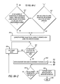
- an upper bound and a lower bound for a respective retiming value for each node in the circuit is computed. This sets a range of retiming values for each node in the circuit. However, a retiming value for a node nearer the lower bound of the retiming value may be preferred as it minimizes backward movement over a node and simplifies the justification problem for registers with initial states (e.g., reset).
- the lower bound of the retiming value for a node is greater than the upper bound of the retiming value, then a retiming of the circuit is not feasible with the selected possibly feasible clock period and the method goes to block 811 .
- the lower bound of the clock period is set to be the previously selected possibly feasible clock period, which was chosen previously in block 810 , and the upper and lower bounds of retiming values for the nodes are reset.
- the process then goes to block 810 where the process of blocks 810 , 812 , and 813 are iterated once again with a different possibly feasible clock period.
- the repeated iteration of the process of blocks 810 , 812 , and 813 using a new possibly feasible clock period may achieve a retiming with a feasible clock period.
- An upper bound of a retiming value is improved if it is decreased.
- a lower bound of a retiming value is improved if it is increased.
- a better upper bound of a retiming value for a node reduces the number of forward register movements over the given node, in one embodiment of the invention.
- a better upper bound and a better lower bound of a retiming value for a node reduce the movement of registers over a node.
- a better upper bound and lower bound on the retiming value may determine that a clock period cannot be achieved by retiming.
- the number of times or iterations that the process of generating new arrival time values and computing upper and lower bounds of retiming values has been performed is tested against a predetermined number. If the number of iterations is less than the predetermined number, then the process goes back to block 812 to further repeat the process of generating new arrival time values and computing upper and lower bounds of retiming values. If the number of iterations is greater than or equal to the predetermined number, then the process goes on to block 818 .
- the process of generating new arrival time values 812 and computing upper and lower bounds of retiming values 813 with a different clock period may be repeated ten times if there is continuing improvement in the computation of upper and lower bounds of retiming values for an achievable retiming.
- a retiming value is computed for each and every node of the circuit within the range of retiming values established by the upper and lower bounds in order to minimize area usage.
- the retiming values are computed to minimize movement of the registers in a circuit and to bias forward register movement over backward register movement. The computation of retiming values to minimize area usage is further described in “Retiming Synchronous Systems” by Leiserson and Saxe previously cited and incorporated by reference as well as “Maheshwari & Sapatnekar I” which was also previously cited and incorporated by reference.
- one or more registers may be moved forward or backward over the node and the process goes to block 822 .
- one or more registers are moved over the node in response to the value of the retiming value for each node that is non-zero. If the retiming value is negative, one or more different registers may be moved forward over the node. If the retiming value is positive, one or more different registers may be moved backward over the node. More detail of the process of register movement 822 over a node is shown and described with reference to FIG. 8B .
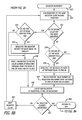
- register movement of registers in the same class are moved together over the nodes.
- Certain types of registers in the register classes may not be moveable over the nodes in the circuit. This may particularly be the case, if the initialization of the register cannot be resolved within the circuit with the given clocking and control signals.
- each differing register in front of the node that is to move backwards over the node is replicated for placement along the fan-in edges coupled into the node. Then the process can go to block 838 .
- a retime value number of registers in front of the node may be moved backward over the node to one or more fan-in edges. The process then goes to block 840 .
- each differing register behind the node that is to move forwards over the node is replicated for placement along the edges coupled out of the node. Then, the process can go to block 838 .
- a retime value number of registers behind the node may be moved forward over the node to one or more fan-out edges. The process then goes to block 840 .
- the clock and control signals and control logic generating the clock and control signals may be adjusted to provide the correct initialization for the register being moved. In some cases, this adjustment process may be best left toward the end of the retiming process, such as at block 828 illustrated in FIG. 8A .
- the logic and control signals to provide the proper initialization settings to the registers may be made as needed.
- the retiming process may go to block 899 and end.
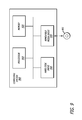
- the computing system 900 includes a processor 910 , a memory 920 , a removable media drive 930 , and a hard disk drive 940 .
- the processor 910 executes instructions residing on a machine-readable medium, such as the hard disk drive 940 , a removable medium (e.g., an optical medium (compact disk (CD), digital video disk (DVD), etc.), a magnetic medium (magnetic disk, a magnetic tape, etc.), or a combination of both.
- the instructions may be loaded from the machine-readable medium into the memory 920 , which may include Random Access Memory (RAM), dynamic RAM (DRAM), etc.
- the processor 910 may retrieve the instructions from the memory 920 and execute the instructions to perform the operations described above.
- any or all of the components and the associated hardware illustrated in FIG. 9 may be used in various embodiments of the system 900 . However, it should be appreciated that other configurations of the system 900 may include more or less devices than those shown in FIG. 9 .
- the embodiments of the invention also relates to an apparatus for automatically performing the operations described herein.
- This apparatus may be specially constructed for the required purposes, or it may comprise a general-purpose computer selectively activated or reconfigured by a computer program stored in the computer.
- the elements of the embodiments of the invention are the code segments to automatically perform an operation.
- the program or code segments can be stored in a machine-readable medium, computer-readable storage medium, processor-readable medium or transmitted by a computer data signal embodied in a carrier wave over a transmission medium or communication link.
- the “processor readable medium” may include any medium that can store or transfer information.
- Examples of the processor readable medium include but are not limited to an electronic circuit, a semiconductor memory device, a read only memory (ROM), a random access memory (RAM), a flash memory, an erasable programmable read only memory (EPROM), a floppy diskette, a CD-ROM, optical storage media such as an optical disk, or magnetic disk storage media such as a hard disk, etc, or any other type of media suitable for storing electronic instructions which can be coupled to a processor, machine, or computer such as through a computer system bus.
- the code segments may be downloaded into the processor readable medium via computer networks such as the Internet, Intranet, etc.
- a constrained minimum period retiming arrival time program is disclosed incorporating constraints on retiming values of gates for computing a lower and upper bound on the clock period achievable by retiming. This speeds up the binary search for the minimum clock period which can be realized by retiming. Moreover, the constrained minimum period retiming arrival time program is based upon retiming graphs formulated from netlists so that the number of edges is reduced to lower the number of computations.
- Efficient computation of lower and upper bounds for the retiming values is disclosed for the constrained minimum period retiming problem.
- the bounds on the retiming values can be used to further bound the retiming values to either determine that a clock period cannot be realized by retiming or to reduce the number of variables and constraints in the network flow formulation.
- the lower bound on the retiming values and the initial solution to the retiming values for each node can be computed very efficiently. It is desirable to generate good lower and upper bounds on the clock period in order to limit the search for a feasible clock period and reduce the testing to determine if a clock period is feasible or not. Moreover, the retiming values may be further constrained to reduce the complexity of the clock period feasibility test and the minimum area optimization.
Landscapes
- Engineering & Computer Science (AREA)
- Computer Hardware Design (AREA)
- Physics & Mathematics (AREA)
- Theoretical Computer Science (AREA)
- Evolutionary Computation (AREA)
- Geometry (AREA)
- General Engineering & Computer Science (AREA)
- General Physics & Mathematics (AREA)
- Design And Manufacture Of Integrated Circuits (AREA)
Abstract
Description
w r(e uv)=w(e uv)+r(v)−r(u) (1)
min(|FI(v)|−|FO(v)|)r(v)
subject to
r(u)−r(v)≦w(e uv) ∀e uv εE
r(u)−r(v)≦W(u,v)−1 ∀D(u,v)≧T (2)
min T
such that l(u)+d((u,v))−T≦l(v) ∀(u,v)εE (3)
-
- subject to
x(i)+c(i,j)−p(i,j)λ≧x(j) (LP6) - where each p(i,j) is a nonnegative integer.
- subject to
a(v):=a r(v)+r(v)T for all vεV and T:=T r (7)
a r(v):=a(v)−r(v)T for all vεV and T r :=T+D (9)
or the rounded down value of the fraction of arrival time over the clock period.
for every gate or node in the solution of the linear program (LP6), then the retimed circuit can achieve a clock period T of Tg+D. A solution is sought to the linear program (LP6) in which every gate has a delay factor of at least one and in which “many” gates have a delay factor of at least the fraction
which is greater than one, if the clock period T is greater than the target clock period Tg or T>Tg.
Claims (27)
Priority Applications (1)
| Application Number | Priority Date | Filing Date | Title |
|---|---|---|---|
| US11/755,425 US7945880B1 (en) | 2007-05-30 | 2007-05-30 | Constraint based retiming of synchronous circuits |
Applications Claiming Priority (1)
| Application Number | Priority Date | Filing Date | Title |
|---|---|---|---|
| US11/755,425 US7945880B1 (en) | 2007-05-30 | 2007-05-30 | Constraint based retiming of synchronous circuits |
Publications (1)
| Publication Number | Publication Date |
|---|---|
| US7945880B1 true US7945880B1 (en) | 2011-05-17 |
Family
ID=43981678
Family Applications (1)
| Application Number | Title | Priority Date | Filing Date |
|---|---|---|---|
| US11/755,425 Active 2030-01-14 US7945880B1 (en) | 2007-05-30 | 2007-05-30 | Constraint based retiming of synchronous circuits |
Country Status (1)
| Country | Link |
|---|---|
| US (1) | US7945880B1 (en) |
Cited By (17)
| Publication number | Priority date | Publication date | Assignee | Title |
|---|---|---|---|---|
| US20090199146A1 (en) * | 2008-02-01 | 2009-08-06 | Hai Zhou | System and method for efficient and optimal minimum area retiming |
| US20110258587A1 (en) * | 2008-01-17 | 2011-10-20 | Lsi Corporation | Signal delay skew reduction system |
| US8181130B1 (en) * | 2009-09-22 | 2012-05-15 | Altera Corporation | Method for jitter reduction by shifting current consumption |
| US8438511B1 (en) * | 2009-12-30 | 2013-05-07 | Cadence Design Systems, Inc. | Minimal logic duplication for preserving reset behavior post-retiming |
| US20150178418A1 (en) * | 2012-12-04 | 2015-06-25 | The Mathworks, Inc. | Model-based retiming with functional equivalence constraints |
| US9275184B1 (en) * | 2014-01-21 | 2016-03-01 | Altera Corporation | Method and apparatus for performing timing closure analysis when performing register retiming |
| US9552456B2 (en) * | 2015-05-29 | 2017-01-24 | Altera Corporation | Methods and apparatus for probing signals from a circuit after register retiming |
| US20170068765A1 (en) * | 2015-09-04 | 2017-03-09 | Altera Corporation | Incremental register retiming of an integrated circuit design |
| US9710591B1 (en) * | 2015-02-20 | 2017-07-18 | Altera Corporation | Method and apparatus for performing register retiming in the presence of timing analysis exceptions |
| US9971858B1 (en) * | 2015-02-20 | 2018-05-15 | Altera Corporation | Method and apparatus for performing register retiming in the presence of false path timing analysis exceptions |
| US20180137226A1 (en) * | 2016-11-17 | 2018-05-17 | Intel Corporation | Methods for verifying retimed circuits with delayed initialization |
| US10282508B1 (en) * | 2016-07-18 | 2019-05-07 | Altera Corporation | Overcoming retiming limitations due to initial conditions conflicts |
| US20190188352A1 (en) * | 2017-12-20 | 2019-06-20 | International Business Machines Corporation | Memory element graph-based placement in integrated circuit design |
| US10354038B1 (en) | 2016-11-15 | 2019-07-16 | Intel Corporation | Methods for bounding the number of delayed reset clock cycles for retimed circuits |
| US10606979B1 (en) * | 2018-06-06 | 2020-03-31 | Xilinx, Inc. | Verifying equivalence of design latency |
| US20210073343A1 (en) | 2019-09-11 | 2021-03-11 | International Business Machines Corporation | Out-of-context feedback hierarchical large block synthesis (hlbs) optimization |
| US20230418322A1 (en) * | 2022-06-27 | 2023-12-28 | eTopus Technology Inc. | Configurable transmitter device based on data rate |
Citations (13)
| Publication number | Priority date | Publication date | Assignee | Title |
|---|---|---|---|---|
| US5822217A (en) * | 1995-12-13 | 1998-10-13 | Synopsys, Inc. | Method and apparatus for improving circuit retiming |
| US6473890B1 (en) * | 1999-09-20 | 2002-10-29 | Takuya Yasui | Clock circuit and method of designing the same |
| US6941541B2 (en) * | 2002-07-19 | 2005-09-06 | Hewlett-Packard Development Company, L.P. | Efficient pipelining of synthesized synchronous circuits |
| US7007262B2 (en) * | 2001-11-15 | 2006-02-28 | Matsushita Electric Industrial Co., Ltd. | High level synthesis method and apparatus |
| US7120883B1 (en) * | 2003-05-27 | 2006-10-10 | Altera Corporation | Register retiming technique |
| US7302657B2 (en) * | 2001-10-29 | 2007-11-27 | Telefonaktiebolaget L M Ericsson (Publ) | Optimization of the design of a synchronous digital circuit |
| US20080276209A1 (en) * | 2007-05-02 | 2008-11-06 | Christoph Albrecht | Optimizing integrated circuit design through use of sequential timing information |
| US7464286B1 (en) * | 2003-01-31 | 2008-12-09 | Altera Corporation | Programmable logic devices with skewed clocking signals |
| US7559040B1 (en) * | 2005-06-02 | 2009-07-07 | Cadence Design Systems, Inc. | Optimization of combinational logic synthesis through clock latency scheduling |
| US7624364B2 (en) * | 2007-05-02 | 2009-11-24 | Cadence Design Systems, Inc. | Data path and placement optimization in an integrated circuit through use of sequential timing information |
| US20090293032A1 (en) * | 2003-05-09 | 2009-11-26 | Levent Oktem | Method and apparatus for circuit design and retiming |
| US7739642B2 (en) * | 2007-05-02 | 2010-06-15 | Cadence Design Systems, Inc. | Optimizing integrated circuit design through balanced combinational slack plus sequential slack |
| US7743354B2 (en) * | 2007-05-02 | 2010-06-22 | Cadence Design Systems, Inc. | Optimizing integrated circuit design through use of sequential timing information |
-
2007
- 2007-05-30 US US11/755,425 patent/US7945880B1/en active Active
Patent Citations (15)
| Publication number | Priority date | Publication date | Assignee | Title |
|---|---|---|---|---|
| US5822217A (en) * | 1995-12-13 | 1998-10-13 | Synopsys, Inc. | Method and apparatus for improving circuit retiming |
| US6473890B1 (en) * | 1999-09-20 | 2002-10-29 | Takuya Yasui | Clock circuit and method of designing the same |
| US7302657B2 (en) * | 2001-10-29 | 2007-11-27 | Telefonaktiebolaget L M Ericsson (Publ) | Optimization of the design of a synchronous digital circuit |
| US7007262B2 (en) * | 2001-11-15 | 2006-02-28 | Matsushita Electric Industrial Co., Ltd. | High level synthesis method and apparatus |
| US6941541B2 (en) * | 2002-07-19 | 2005-09-06 | Hewlett-Packard Development Company, L.P. | Efficient pipelining of synthesized synchronous circuits |
| US7464286B1 (en) * | 2003-01-31 | 2008-12-09 | Altera Corporation | Programmable logic devices with skewed clocking signals |
| US20090293032A1 (en) * | 2003-05-09 | 2009-11-26 | Levent Oktem | Method and apparatus for circuit design and retiming |
| US7120883B1 (en) * | 2003-05-27 | 2006-10-10 | Altera Corporation | Register retiming technique |
| US7689955B1 (en) * | 2003-05-27 | 2010-03-30 | Altera Corporation | Register retiming technique |
| US7559040B1 (en) * | 2005-06-02 | 2009-07-07 | Cadence Design Systems, Inc. | Optimization of combinational logic synthesis through clock latency scheduling |
| US20080276209A1 (en) * | 2007-05-02 | 2008-11-06 | Christoph Albrecht | Optimizing integrated circuit design through use of sequential timing information |
| US7624364B2 (en) * | 2007-05-02 | 2009-11-24 | Cadence Design Systems, Inc. | Data path and placement optimization in an integrated circuit through use of sequential timing information |
| US20100115477A1 (en) * | 2007-05-02 | 2010-05-06 | Cadence Design Systems, Inc. | Optimizing integrated circuit design through use of sequential timing information |
| US7739642B2 (en) * | 2007-05-02 | 2010-06-15 | Cadence Design Systems, Inc. | Optimizing integrated circuit design through balanced combinational slack plus sequential slack |
| US7743354B2 (en) * | 2007-05-02 | 2010-06-22 | Cadence Design Systems, Inc. | Optimizing integrated circuit design through use of sequential timing information |
Non-Patent Citations (14)
| Title |
|---|
| Chu et al.; "Retiming with interconnect and gate delay"; Publication Year: 2003; Computer Aided Design, ICCAD-2003; International Conference on; , pp. 221-226. * |
| Eckly, K. ; Madre, J. ; Zepter, P. ; Legl, C. A Practical Approach to Multiple-Class Retiming. 1999. 1-6. ACM, New Orleans, Louisiana. |
| Ekpanyapong et al.; "Statistical Bellman-Ford algorithm with an application to retiming"; Publication Year: 2006; Design Automation, 2006. Asia and South Pacific Conference on. * |
| Legl, C. ; Vanbekbergen, P. ; Wang, A. Retiming of Edge-Triggered Circuits with Multiple Clocka and Load Enables. May 1997. 1-4. Tahoe City, CA. |
| Leiserson, C. ; Saxe, J. ; Retiming Synchronous Circuitry. 1991. 5-35. Springer-Verlag New York Inc. |
| Liu et al.; "Data flow partitioning with clock period and latency constraints"; Publication Year: 1997; Circuits and Systems I: Fundamental Theory and Applications, IEEE Transactions on; vol. 44 , Issue: 3; pp. 210-220. * |
| Maheshwari, N. ; Sapatnekar, S. Efficient Retiming of Large Circuits. IEEE Transactions on Very Large Scale Integration Systems. Mar. 1998. 74-83. vol. 6. |
| Maheshwari, N. ; Sapatnekar, S. Retiming Control Logic. Elsevier Science, Amsterdam 1-20. 1999. |
| O'Neil et al.; "Retiming synchronous data-flow graphs to reduce execution time"; Publication Year: 2001; Signal Processing, IEEE Transactions on; vol. 49 , Issue: 10; pp. 2397-2407. * |
| Pan, P. Continuous Retiming: Algorithms and Applications. 1997.1-6. ICCD. |
| Papaefthymiou, M. Understanding Retiming through Maximum Average-Delay Cycles. Mathematical Systems Theory. No. 27. 1-22. 1994. |
| Sapatnekar, S. ; Deokar, R. Utilizing the Retiming-Skew Equivalence in a Practical Algorithm for Retiming Large Circuits.IEEE Transactions on Computer-Aided Design of Integrated Circuits and Systems. 1996. 1237-1248. vol. 15. |
| Shenoy, N. ; Rudell, R. Efficient Implementation of Retiming. 226-233. 1994. ACM. |
| Touati, H. ; Brayton, R.. Computing the Initial States of Retimed Circuits. IEEE Transactions on Computer-Aided Design of Integrated Circuits and Systems. Jan. 1993. 157-162. vol. 12. |
Cited By (31)
| Publication number | Priority date | Publication date | Assignee | Title |
|---|---|---|---|---|
| US8239813B2 (en) * | 2008-01-17 | 2012-08-07 | Lsi Corporation | Method and apparatus for balancing signal delay skew |
| US20110258587A1 (en) * | 2008-01-17 | 2011-10-20 | Lsi Corporation | Signal delay skew reduction system |
| US8516425B2 (en) | 2008-01-17 | 2013-08-20 | Lsi Corporation | Method and computer program for generating grounded shielding wires for signal wiring |
| US8813001B2 (en) * | 2008-02-01 | 2014-08-19 | Northwestern University | System and method for efficient and optimal minimum area retiming |
| US20090199146A1 (en) * | 2008-02-01 | 2009-08-06 | Hai Zhou | System and method for efficient and optimal minimum area retiming |
| US8181130B1 (en) * | 2009-09-22 | 2012-05-15 | Altera Corporation | Method for jitter reduction by shifting current consumption |
| US8438511B1 (en) * | 2009-12-30 | 2013-05-07 | Cadence Design Systems, Inc. | Minimal logic duplication for preserving reset behavior post-retiming |
| US20150178418A1 (en) * | 2012-12-04 | 2015-06-25 | The Mathworks, Inc. | Model-based retiming with functional equivalence constraints |
| US9779195B2 (en) * | 2012-12-04 | 2017-10-03 | The Mathworks, Inc. | Model-based retiming with functional equivalence constraints |
| US9275184B1 (en) * | 2014-01-21 | 2016-03-01 | Altera Corporation | Method and apparatus for performing timing closure analysis when performing register retiming |
| US10339238B2 (en) | 2015-02-20 | 2019-07-02 | Altera Corporation | Method and apparatus for performing register retiming in the presence of timing analysis exceptions |
| US10671781B2 (en) | 2015-02-20 | 2020-06-02 | Altera Corporation | Method and apparatus for performing register retiming in the presence of false path timing analysis exceptions |
| US9710591B1 (en) * | 2015-02-20 | 2017-07-18 | Altera Corporation | Method and apparatus for performing register retiming in the presence of timing analysis exceptions |
| US9971858B1 (en) * | 2015-02-20 | 2018-05-15 | Altera Corporation | Method and apparatus for performing register retiming in the presence of false path timing analysis exceptions |
| US9552456B2 (en) * | 2015-05-29 | 2017-01-24 | Altera Corporation | Methods and apparatus for probing signals from a circuit after register retiming |
| US10387603B2 (en) | 2015-09-04 | 2019-08-20 | Altera Corporation | Incremental register retiming of an integrated circuit design |
| US20170068765A1 (en) * | 2015-09-04 | 2017-03-09 | Altera Corporation | Incremental register retiming of an integrated circuit design |
| US9996652B2 (en) * | 2015-09-04 | 2018-06-12 | Altera Corporation | Incremental register retiming of an integrated circuit design |
| US10949599B2 (en) | 2016-07-18 | 2021-03-16 | Altera Corporation | Overcoming retiming limitations due to initial conditions conflicts |
| US10282508B1 (en) * | 2016-07-18 | 2019-05-07 | Altera Corporation | Overcoming retiming limitations due to initial conditions conflicts |
| US10354038B1 (en) | 2016-11-15 | 2019-07-16 | Intel Corporation | Methods for bounding the number of delayed reset clock cycles for retimed circuits |
| US10372850B2 (en) * | 2016-11-17 | 2019-08-06 | Intel Corporation | Methods for verifying retimed circuits with delayed initialization |
| US20180137226A1 (en) * | 2016-11-17 | 2018-05-17 | Intel Corporation | Methods for verifying retimed circuits with delayed initialization |
| US10558775B2 (en) * | 2017-12-20 | 2020-02-11 | International Business Machines Corporation | Memory element graph-based placement in integrated circuit design |
| US20190188352A1 (en) * | 2017-12-20 | 2019-06-20 | International Business Machines Corporation | Memory element graph-based placement in integrated circuit design |
| US11080443B2 (en) | 2017-12-20 | 2021-08-03 | International Business Machines Corporation | Memory element graph-based placement in integrated circuit design |
| US10606979B1 (en) * | 2018-06-06 | 2020-03-31 | Xilinx, Inc. | Verifying equivalence of design latency |
| US20210073343A1 (en) | 2019-09-11 | 2021-03-11 | International Business Machines Corporation | Out-of-context feedback hierarchical large block synthesis (hlbs) optimization |
| US11030367B2 (en) | 2019-09-11 | 2021-06-08 | International Business Machines Corporation | Out-of-context feedback hierarchical large block synthesis (HLBS) optimization |
| US20230418322A1 (en) * | 2022-06-27 | 2023-12-28 | eTopus Technology Inc. | Configurable transmitter device based on data rate |
| US11907004B2 (en) * | 2022-06-27 | 2024-02-20 | eTopus Technology Inc. | Configurable transmitter device based on data rate |
Similar Documents
| Publication | Publication Date | Title |
|---|---|---|
| US7945880B1 (en) | Constraint based retiming of synchronous circuits | |
| US8832614B2 (en) | Technology mapping for threshold and logic gate hybrid circuits | |
| US20180203956A1 (en) | Neural network based physical synthesis for circuit designs | |
| US20060085781A1 (en) | Library for computer-based tool and related system and method | |
| Gowda et al. | Identification of threshold functions and synthesis of threshold networks | |
| Testa et al. | Logic synthesis for established and emerging computing | |
| US8381142B1 (en) | Using a timing exception to postpone retiming | |
| Bruneel et al. | Dynamic data folding with parameterizable FPGA configurations | |
| Ozdal et al. | Algorithms for gate sizing and device parameter selection for high-performance designs | |
| Janakiraman et al. | Multi-objective module partitioning design for dynamic and partial reconfigurable system-on-chip using genetic algorithm | |
| US10417374B1 (en) | Method and apparatus for performing register retiming by utilizing native timing-driven constraints | |
| Sze et al. | Path based buffer insertion | |
| Chen et al. | Simultaneous timing-driven placement and duplication | |
| Maheshwari et al. | Optimizing large multiphase level-clocked circuits | |
| Coe et al. | A hardware memetic accelerator for VLSI circuit partitioning | |
| Li et al. | An automatic transistor-level tool for GRM FPGA interconnect circuits optimization | |
| Bommu et al. | Retiming-based factorization for sequential logic optimization | |
| Mahzoon et al. | Polynomial formal verification of general tree-like circuits | |
| Ammes et al. | Two-Level and Multilevel Approximate Logic Synthesis | |
| Tu et al. | Logic Synthesis | |
| Neophytou et al. | Path representation in circuit netlists using linear-sized ZDDs with optimal variable ordering | |
| US11017137B2 (en) | Efficient projection based adjustment evaluation in static timing analysis of integrated circuits | |
| Kravets et al. | Sequential logic synthesis using symbolic bi-decomposition | |
| Soyata | Incorporating circuit-level information into the retiming process | |
| US20230239136A1 (en) | Pipelined Galois Counter Mode Hash Circuit |
Legal Events
| Date | Code | Title | Description |
|---|---|---|---|
| AS | Assignment |
Owner name: CADENCE DESIGN SYSTEMS, INC., CALIFORNIA Free format text: ASSIGNMENT OF ASSIGNORS INTEREST;ASSIGNORS:ALBRECHT, CHRISTOPH;RICHTER, SASCHA;REEL/FRAME:019356/0977 Effective date: 20070530 |
|
| FEPP | Fee payment procedure |
Free format text: PAYOR NUMBER ASSIGNED (ORIGINAL EVENT CODE: ASPN); ENTITY STATUS OF PATENT OWNER: LARGE ENTITY Free format text: PAYER NUMBER DE-ASSIGNED (ORIGINAL EVENT CODE: RMPN); ENTITY STATUS OF PATENT OWNER: LARGE ENTITY |
|
| STCF | Information on status: patent grant |
Free format text: PATENTED CASE |
|
| FPAY | Fee payment |
Year of fee payment: 4 |
|
| MAFP | Maintenance fee payment |
Free format text: PAYMENT OF MAINTENANCE FEE, 8TH YEAR, LARGE ENTITY (ORIGINAL EVENT CODE: M1552); ENTITY STATUS OF PATENT OWNER: LARGE ENTITY Year of fee payment: 8 |
|
| MAFP | Maintenance fee payment |
Free format text: PAYMENT OF MAINTENANCE FEE, 12TH YEAR, LARGE ENTITY (ORIGINAL EVENT CODE: M1553); ENTITY STATUS OF PATENT OWNER: LARGE ENTITY Year of fee payment: 12 |